JP3688891B2 - Imaging device - Google Patents
Imaging device Download PDFInfo
- Publication number
- JP3688891B2 JP3688891B2 JP15279598A JP15279598A JP3688891B2 JP 3688891 B2 JP3688891 B2 JP 3688891B2 JP 15279598 A JP15279598 A JP 15279598A JP 15279598 A JP15279598 A JP 15279598A JP 3688891 B2 JP3688891 B2 JP 3688891B2
- Authority
- JP
- Japan
- Prior art keywords
- sensitivity correction
- light receiving
- pixels
- correction
- imaging apparatus
- Prior art date
- Legal status (The legal status is an assumption and is not a legal conclusion. Google has not performed a legal analysis and makes no representation as to the accuracy of the status listed.)
- Expired - Fee Related
Links
Images


Description
【0001】
【発明の属する技術分野】
この発明は、例えば複数の画素から構成される受光素子を有する撮像装置の改良に関する。
【0002】
【従来の技術】
一般に、例えば赤外線撮像装置の赤外線受光素子は、複数の画素により構成されている。ところで、赤外線受光素子には、画素毎の特性にバラツキがあり、満足な赤外線画像を得るためには、画素毎の感度補正(オフセット補正,ゲイン補正)を行なう必要がある。
【0003】
そこで、従来では、感度補正の手段として、光路内に光路を遮るようなシャッタ、つまり均一温度と見なせるシャッタを設け、感度補正時にシャッタを閉じるという方法を用いたり、また赤外線集光光学系の前方を均一温度と見なせる遮蔽板等で遮るという方法を用いている。
【0004】
ところが、上記方法では、遮蔽板等のシャッタ機構を設けると集光光学系が複雑な構成となったり、また、遮蔽板等で遮蔽するという動作のため感度補正の作業効率が非常に悪いという問題が生じている。また、精度良く感度補正を行なうためには、2種類以上の温度をもつシャッタ、あるいは遮蔽板を用意しなければならず、このため、部品数の増加による装置の大型化を招き、さらに装置のコストが高くなるという不都合が生じることがある。
【0005】
【発明が解決しようとする課題】
以上のように、従来の撮像装置では、集光光学系の光路上に感度補正を行なうためのシャッタ機構を設けていることにより、集光光学系が複雑化したり、また感度補正の作業効率が悪いという問題を有している。さらに、精度良く感度補正を行なうために、2種類以上の温度をもつシャッタ、あるいは遮蔽板を用意する必要があり、このため、装置の大型化、もしくは装置のコストが高くなるという不都合を有している。
この発明の目的は、装置を複雑化させることなく、感度補正を容易にかつ効率的に行ない得る撮像装置を提供することにある。
【0006】
【課題を解決するための手段】
この発明に係る撮像装置は、複数の画素を有し、外部からの光を該複数の画素で受光する受光手段と、この受光手段の周囲を覆うドームと、このドームの内面に設けられるものであって、互いに放射率が異なる複数の感度補正面と、受光手段を複数の感度補正面に指向させることで、受光手段の複数の画素の出力を一致させるように補正する感度補正手段とを備えるようにしたものである。
【0007】
この構成によれば、受光手段の周囲を覆うドームの内面に互いに異なる放射率を有する複数の感度補正面を設けるようにし、受光手段を複数の感度補正面に指向させることにより、受光手段の複数の画素の出力が一致するように補正されるので、集光光学系を複雑化させずに済む。
【0008】
また、複数の感度補正面の有する異なる放射率で、互いに異なる温度を実現するようにしているので、別途に2種類以上のシャッタや遮蔽板等を設ける必要がなく、受光手段を複数の感度補正面に指向させるのみで、各温度に対応して複数の画素の出力がそれぞれ一致するように補正されるので、効率的な補正処理が行なわれ、かつ高精度な感度補正が実現できる。このため、装置の小型化及び低コスト化にも寄与できる。
【0009】
【発明の実施の形態】
以下、この発明の実施の形態を図面を参照して詳細に説明する。
図1は、この発明の一実施の形態における例えば赤外線撮像装置のほぼ全体を示し、図2は、この撮像装置の断面を示している。
【0010】
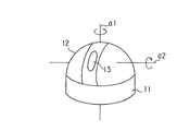
図1において、図中符号11は軸a1回りに回転可能となるように図示しない固定部に支持される基板であり、その上に外部からの光を受光する例えば赤外線受光素子、つまりCCD(Charge Couple Device)素子からなる集光光学部(図2では符号21で示す)を設けている。また、図中符号12は集光光学部21の周囲を覆う半球状のドームで、その球表面に外部からの光を集光光学部21に導く窓13を形成している。
【0011】
集光光学部21は、図2に示すように、基板11上に固定された支持部211と、この支持部211により軸a2回りに回動可能となるように支持された受光部212とから構成されている。また、受光部212は、その内部に複数の画素を有している。すなわち、集光光学部21は、基板11を軸a1回りに回転、もしくは受光部212を軸a2回りの方向(図2中では矢印b1で示す方向)に回動させることにより、外部からの光を窓13を介し受光部212内の図示しないレンズにて受光する。
【0012】
また、ドーム12の内面には、受光部212の回動範囲内に集光光学部21に対して感度補正を行なうための感度補正面14a,14bが設けられている。ここで、感度補正面14a,14bについて図3〜図5を参照して説明する。なお、図3は、ドーム12を上方から見た感度補正面14a,14bの状態を示しており、図4は、集光光学部21における感度補正時の動作を示しており、図5は、感度補正により得られる結果を示している。また、図5(a),(b)において、縦軸は画素出力を示し、横軸は温度を示しており、特に左から右へ進むにつれて高温となる。
【0013】
図3において、ドーム12の内面に設けられた感度補正面14a,14bは、それぞれ受光部212で受光可能な面積で形成されており、また、互いに異なる放射率を有している。なお、この発明では、2種類の温度を実現する方法として放射率の違いを利用することを特徴とする。
【0014】
一般に物質は、それぞれ異なる放射率を有していることが知られている。また、同じ物質でも表面の形態(例えば研磨して光沢のある状態にしたもの、あるいはペイントを施したもの)が異なることが知られている。そこで、この発明は、物質の違い、あるいは処理の違いから生じる放射率の違いから生じる放射率の違いを利用することにより、感度補正のための等価的に異なる温度を実現することを特徴とするものである。
【0015】
すなわち、この実施の形態では、感度補正面14a,14bは、例えば金属と布であるか、もしくは同じ物質を用いて一方にペイントを施し、他方には何も施さないようにしたものである。
【0016】
図4において、集光光学部21は、感度補正時に、その受光部212の受光側を感度補正面14a,14bに指向させることにより、その受光部212内の複数の画素(図5中では4画素)の出力が図5(a)のバラツキのある状態から図5(b)の状態に補正される。この場合、一定温度(一定赤外線受光量)に対して各画素の出力が等しくなるように補正するオフセット補正と、温度変化(赤外線受光量変化)に対する各画素の出力変化量が等しくなるように画素毎の利得を補正するゲイン補正とが行われる。なお、感度補正は、場合によってオフセット補正及びゲイン補正のうちいずれか一方の補正を行なうようにしてもよい。
【0017】
したがって、上記実施の形態によれば、集光光学部21の周囲を覆うドーム12の内面に互いに異なる放射率を有する感度補正面14a,14bを設けるようにし、集光光学部21を感度補正面14a,14bに指向させることにより、集光光学部21内の複数の画素の出力が一致するように補正されるので、光学系部品の複雑化を防止できる。
【0018】
また、感度補正面14a,14bの有する異なる放射率で、互いに異なる温度を実現するようにしているので、別途に2種類以上のシャッタや遮蔽板等を設ける必要がなく、支持部211により回動自在に支持された受光部212の受光側を感度補正面14a,14bに指向させるのみで、各温度に対応して複数の画素の出力がそれぞれ一致するように補正されるので、効率的な補正処理が行なわれ、かつ高精度な感度補正が実現できる。
【0019】
さらに、集光光学部21を既知のドーム12内に設けられた感度補正面14a,14bに指向させるのみで、高精度な補正を実現できるので、わざわざ光路を遮蔽するような機構及びこの機構の動力源を備える必要がなく、このため、装置の小型化及び低コスト化にも貢献できる。
【0020】
なお、上記実施の形態の感度補正手段として、ドーム12内のどの箇所に放射率が異なる物質部分を設けるか、あるいは異なる処理を施すかは、対象となる赤外線撮像装置全体の構造等によって自由に決定できることはもちろんのことである。また、上記実施の形態では、赤外線受光素子をもつものを対象として説明しているが、赤外線以外の受光素子を用いた撮像装置であっても、異なる複数の放射率を利用するものであれば、実施できることはもちろんのことである。
【0021】
また、この発明は、上記実施の形態の範囲に必ずしも限定されるものではなく、その他この要旨を逸脱しない範囲で種々変形して実施できることはもちろんのことである。
【0022】
【発明の効果】
以上詳述したようにこの発明によれば、装置を複雑化させることなく、感度補正を容易にかつ効率的に行ない得る撮像装置を提供することができる。
【図面の簡単な説明】
【図1】この発明の一実施の形態を示す斜視図
【図2】同実施の形態の要部を示す断面図。
【図3】同実施の形態におけるドームを上方から見た場合の感度補正面の配置状態を示す図。
【図4】同実施の形態における感度補正時の動作例を説明するために示す断面図。
【図5】同実施の形態における感度補正により得られる結果を説明するために示す特性図。
【符号の説明】
11…基板、
12…ドーム、
13…窓、
14a,14b…感度補正面、
21…集光光学部、
211…支持部、
212…受光部。[0001]
BACKGROUND OF THE INVENTION
The present invention relates to an improvement of an imaging apparatus having a light receiving element composed of a plurality of pixels, for example.
[0002]
[Prior art]
In general, for example, an infrared light receiving element of an infrared imaging device includes a plurality of pixels. By the way, the characteristics of each infrared light receiving element vary, and it is necessary to perform sensitivity correction (offset correction, gain correction) for each pixel in order to obtain a satisfactory infrared image.
[0003]
Therefore, conventionally, as a means for correcting the sensitivity, a shutter that blocks the optical path in the optical path, that is, a shutter that can be regarded as a uniform temperature is provided, and the shutter is closed at the time of sensitivity correction, or in front of the infrared condensing optical system. Is shielded by a shielding plate or the like that can be regarded as a uniform temperature.
[0004]
However, in the above method, when a shutter mechanism such as a shielding plate is provided, the condensing optical system has a complicated configuration, and the work efficiency of sensitivity correction is very poor due to the operation of shielding with a shielding plate or the like. Has occurred. In addition, in order to perform sensitivity correction with high accuracy, it is necessary to prepare a shutter or a shielding plate having two or more types of temperatures, which leads to an increase in the size of the device due to an increase in the number of parts, and further There may be an inconvenience of high cost.
[0005]
[Problems to be solved by the invention]
As described above, in the conventional image pickup apparatus, since the shutter mechanism for performing sensitivity correction is provided on the optical path of the condensing optical system, the condensing optical system becomes complicated and the work efficiency of the sensitivity correction is reduced. Has the problem of being bad. Furthermore, in order to perform sensitivity correction with high accuracy, it is necessary to prepare a shutter or a shielding plate having two or more types of temperatures, which has the disadvantage of increasing the size of the device or increasing the cost of the device. ing.
An object of the present invention is to provide an imaging apparatus capable of performing sensitivity correction easily and efficiently without complicating the apparatus.
[0006]
[Means for Solving the Problems]
An image pickup apparatus according to the present invention includes a plurality of pixels, a light receiving unit that receives light from the outside with the plurality of pixels, a dome that covers the periphery of the light receiving unit, and an inner surface of the dome. there are a plurality of sensitivity correction surface emissivity are different from each other, by directing the light receiving means into a plurality of sensitivity correction surface, and a sensitivity correction unit configured to correct so as to match the output of a plurality of pixels of the light receiving means It is what I did.
[0007]
According to this configuration, a plurality of sensitivity correction surfaces having different emissivities are provided on the inner surface of the dome that covers the periphery of the light receiving means, and the light receiving means is directed to the plurality of sensitivity correction surfaces, thereby providing a plurality of light receiving means. Therefore, the condensing optical system does not have to be complicated.
[0008]
In addition, since different temperatures are realized with different emissivities of a plurality of sensitivity correction surfaces, it is not necessary to separately provide two or more types of shutters, shielding plates, etc., and the light receiving means can be adjusted to a plurality of sensitivities. By simply directing it to the surface, correction is performed so that the outputs of a plurality of pixels coincide with each temperature, so that efficient correction processing is performed and highly accurate sensitivity correction can be realized. For this reason, it can contribute also to size reduction and cost reduction of an apparatus.
[0009]
DETAILED DESCRIPTION OF THE INVENTION
Hereinafter, embodiments of the present invention will be described in detail with reference to the drawings.
FIG. 1 shows almost the entire infrared imaging device, for example, according to an embodiment of the present invention, and FIG. 2 shows a cross section of the imaging device.
[0010]
In FIG. 1, reference numeral 11 denotes a substrate supported by a fixed portion (not shown) so as to be rotatable about an axis a1, and an infrared light receiving element for receiving light from the outside, for example, a CCD (Charge). A condensing optical unit (indicated by
[0011]
As shown in FIG. 2, the condensing
[0012]
Further, on the inner surface of the
[0013]
In FIG. 3,
[0014]
It is generally known that substances have different emissivities. In addition, it is known that even the same material has a different surface form (for example, polished to be glossy or painted). Therefore, the present invention is characterized in that equivalently different temperatures for sensitivity correction are realized by utilizing a difference in emissivity resulting from a difference in emissivity resulting from a difference in materials or a difference in processing. Is.
[0015]
That is, in this embodiment, the
[0016]
In FIG. 4, the condensing
[0017]
Therefore, according to the above embodiment, the sensitivity correction surfaces 14a and 14b having different emissivities are provided on the inner surface of the
[0018]
Further, since different temperatures are realized with different emissivities of the sensitivity correction surfaces 14a and 14b, it is not necessary to separately provide two or more types of shutters, shielding plates, etc., and the
[0019]
Furthermore, since the highly accurate correction can be realized only by directing the condensing
[0020]
It should be noted that, as the sensitivity correction means of the above-described embodiment, it is freely determined in which location in the dome 12 a material portion having a different emissivity or a different process is applied depending on the structure of the entire target infrared imaging device. Of course you can decide. Moreover, although the said embodiment demonstrated as an object what has an infrared rays light receiving element, even if it is an imaging device using light receiving elements other than infrared rays, as long as it utilizes several different emissivities, Of course, it can be implemented.
[0021]
Further, the present invention is not necessarily limited to the scope of the above embodiment, and it goes without saying that various modifications can be made without departing from the scope of the present invention.
[0022]
【The invention's effect】
As described above in detail, according to the present invention, it is possible to provide an imaging apparatus capable of performing sensitivity correction easily and efficiently without complicating the apparatus.
[Brief description of the drawings]
FIG. 1 is a perspective view showing an embodiment of the present invention. FIG. 2 is a cross-sectional view showing a main part of the embodiment.
FIG. 3 is a view showing an arrangement state of sensitivity correction surfaces when the dome is viewed from above in the same embodiment;
FIG. 4 is a cross-sectional view for explaining an operation example at the time of sensitivity correction in the embodiment.
FIG. 5 is a characteristic diagram for explaining a result obtained by sensitivity correction in the embodiment;
[Explanation of symbols]
11 ... substrate
12 ... Dome,
13 ... window,
14a, 14b ... sensitivity correction surface,
21 ... Condensing optical part,
211 ... support part,
212: a light receiving unit.
Claims (5)
この受光手段の周囲を覆うドームと、
このドームの内面に設けられるものであって、互いに放射率が異なる複数の感度補正面と、
前記受光手段を前記複数の感度補正面に指向させることで、前記受光手段の複数の画素の出力を一致させるように補正する感度補正手段とを具備してなることを特徴とする撮像装置。A light receiving means having a plurality of pixels and receiving light from the outside by the plurality of pixels;
A dome covering the periphery of the light receiving means;
A plurality of sensitivity correction surfaces provided on the inner surface of the dome, each having a different emissivity , and
It said light receiving means by directing said plurality of sensitivity correction surface, an imaging apparatus characterized by comprising; and a sensitivity correction unit configured to correct so as to match the output of a plurality of pixels of the light receiving means.
Priority Applications (1)
| Application Number | Priority Date | Filing Date | Title |
|---|---|---|---|
| JP15279598A JP3688891B2 (en) | 1998-06-02 | 1998-06-02 | Imaging device |
Applications Claiming Priority (1)
| Application Number | Priority Date | Filing Date | Title |
|---|---|---|---|
| JP15279598A JP3688891B2 (en) | 1998-06-02 | 1998-06-02 | Imaging device |
Publications (2)
| Publication Number | Publication Date |
|---|---|
| JPH11346330A JPH11346330A (en) | 1999-12-14 |
| JP3688891B2 true JP3688891B2 (en) | 2005-08-31 |
Family
ID=15548323
Family Applications (1)
| Application Number | Title | Priority Date | Filing Date |
|---|---|---|---|
| JP15279598A Expired - Fee Related JP3688891B2 (en) | 1998-06-02 | 1998-06-02 | Imaging device |
Country Status (1)
| Country | Link |
|---|---|
| JP (1) | JP3688891B2 (en) |
Families Citing this family (2)
| Publication number | Priority date | Publication date | Assignee | Title |
|---|---|---|---|---|
| US8958911B2 (en) * | 2012-02-29 | 2015-02-17 | Irobot Corporation | Mobile robot |
| JP5970965B2 (en) * | 2012-06-07 | 2016-08-17 | 日本電気株式会社 | Imaging device |
-
1998
- 1998-06-02 JP JP15279598A patent/JP3688891B2/en not_active Expired - Fee Related
Also Published As
| Publication number | Publication date |
|---|---|
| JPH11346330A (en) | 1999-12-14 |
Similar Documents
| Publication | Publication Date | Title |
|---|---|---|
| US7609302B2 (en) | Correction of non-uniform sensitivity in an image array | |
| JPH0481178A (en) | Dc offset correction method for irccd detector | |
| US20110211077A1 (en) | Adaptive imaging using digital light processing | |
| US9503698B2 (en) | Image sensor with shading detection | |
| JPH0313074A (en) | Picture processing system | |
| US8670069B2 (en) | Imaging device having an angle adjusting device for an image sensor | |
| EP0830013A3 (en) | Focal plane array calibration method | |
| US20080197290A1 (en) | Camera-based x-ray digital image detector | |
| EP0132345A2 (en) | Infra-red optical systems | |
| JP3688891B2 (en) | Imaging device | |
| JPH05231934A (en) | Scanning method and apparatus for photoelectron camera having high resolution and wide filed of view | |
| JP3382530B2 (en) | Optical imaging device | |
| US6546076B1 (en) | Digital high resolution x-ray imaging utilizing an imaging sensor | |
| JPH0533867B2 (en) | ||
| JPS62188952A (en) | Film image information reader | |
| JP2778577B2 (en) | Light beam angle detector | |
| JP3267877B2 (en) | Aspheric element for infrared imaging system | |
| JPH0277001A (en) | Prism for video camera | |
| EP3598730A1 (en) | Light field capturing system and corresponding calibration device, method and computer program product | |
| JPH01121816A (en) | Solid-state image pickup device | |
| JPH05227485A (en) | Infrared image pickup device | |
| JP3024530B2 (en) | Rotary imaging device | |
| JPS6040228B2 (en) | infrared monitoring device | |
| JPH0720214B2 (en) | Infrared imaging device signal correction method | |
| JP3670458B2 (en) | Image reading device |
Legal Events
| Date | Code | Title | Description |
|---|---|---|---|
| A977 | Report on retrieval |
Free format text: JAPANESE INTERMEDIATE CODE: A971007 Effective date: 20050217 |
|
| A131 | Notification of reasons for refusal |
Free format text: JAPANESE INTERMEDIATE CODE: A131 Effective date: 20050222 |
|
| A521 | Request for written amendment filed |
Free format text: JAPANESE INTERMEDIATE CODE: A523 Effective date: 20050415 |
|
| TRDD | Decision of grant or rejection written | ||
| A01 | Written decision to grant a patent or to grant a registration (utility model) |
Free format text: JAPANESE INTERMEDIATE CODE: A01 Effective date: 20050607 |
|
| A61 | First payment of annual fees (during grant procedure) |
Free format text: JAPANESE INTERMEDIATE CODE: A61 Effective date: 20050609 |
|
| FPAY | Renewal fee payment (event date is renewal date of database) |
Free format text: PAYMENT UNTIL: 20090617 Year of fee payment: 4 |
|
| FPAY | Renewal fee payment (event date is renewal date of database) |
Free format text: PAYMENT UNTIL: 20090617 Year of fee payment: 4 |
|
| FPAY | Renewal fee payment (event date is renewal date of database) |
Free format text: PAYMENT UNTIL: 20100617 Year of fee payment: 5 |
|
| FPAY | Renewal fee payment (event date is renewal date of database) |
Free format text: PAYMENT UNTIL: 20100617 Year of fee payment: 5 |
|
| FPAY | Renewal fee payment (event date is renewal date of database) |
Free format text: PAYMENT UNTIL: 20110617 Year of fee payment: 6 |
|
| FPAY | Renewal fee payment (event date is renewal date of database) |
Free format text: PAYMENT UNTIL: 20120617 Year of fee payment: 7 |
|
| LAPS | Cancellation because of no payment of annual fees |