JP3687585B2 - Variable focus lens device - Google Patents
Variable focus lens device Download PDFInfo
- Publication number
- JP3687585B2 JP3687585B2 JP2001309361A JP2001309361A JP3687585B2 JP 3687585 B2 JP3687585 B2 JP 3687585B2 JP 2001309361 A JP2001309361 A JP 2001309361A JP 2001309361 A JP2001309361 A JP 2001309361A JP 3687585 B2 JP3687585 B2 JP 3687585B2
- Authority
- JP
- Japan
- Prior art keywords
- substrate
- hole
- variable focus
- focus lens
- elastic member
- Prior art date
- Legal status (The legal status is an assumption and is not a legal conclusion. Google has not performed a legal analysis and makes no representation as to the accuracy of the status listed.)
- Expired - Fee Related
Links
Images


Description
【0001】
【発明の属する技術分野】
本発明は、焦点可変レンズ装置に関するものである。
【0002】
【従来の技術】
従来焦点可変レンズ装置においては、液晶などを用いてレンズの屈折率を変動させたり、レンズ自体をアクチュエータで動かして焦点を変化させていた。また、レンズ内部に液体を封入するものについては、特開平7−49404や特開平10−269599に見られる。これらはいずれも外部の駆動源によりレンズの厚みを変化させ、焦点距離を変化させていた。
【0003】
【発明が解決しようとする課題】
しかし、これらの駆動源は電磁力方式や圧電方式で駆動させるためレンズ装置全体を小型化することができず、また消費電力も大きかった。さらには特開平7−49404においては、レンズの厚みを変化させるためにレンズ部にある液体の量を変化させるが、レンズ部にある液体の量を変化させるときの液体の流入または流出方向が一方向であるため、液体の量が変化して均一なレンズ形状になるまで、すなわちレンズとして正しく機能するまでには時間がかかり高速応答性は低かった。
【0004】
また、特開平10−269599においては、内部の液体の量を変化させないでレンズの厚みを変化させるため、厚みの可変量は小さく焦点可変距離も小さかった。
【0005】
本発明はこのような事情に鑑みてなされたもので、半導体プロセスを用いた小型の焦点可変レンズ装置の提供を目的とする。
【0006】
【課題を解決するための手段】
上記の課題を解決するため請求項1の発明においては、シリコンからなる第1の基板と前記第1の基板と対向して接着されている光透過性を有する第2の基板を備え、前記第1の基板には前記第1の基板と前記第2の基板が接着されている側から前記第1の基板を厚み方向にエッチングによって円形の第1の穴と第2の穴が開けられており、前記第1の穴と前記第2の穴は前記第1の基板と前記第2の基板が接着されている側で連通しており、前記第1の基板における前記第2の基板が接着されていない側の表面は前記第1の穴と前記第2の穴を一体的に覆うように前記第1の基板に不純物をドーピングして形成した光透過性と導電性を有する膜状の弾性部材となっており、前記第1の基板と前記第2の基板と前記弾性部材で形成される空間に変形可能な光透過性物質が封入されており、前記弾性部材のうち前記第2の穴に対向する箇所であってかつ前記第1の基板と反対側にポリシリコン膜に不純物をドーピングした固定電極が形成されており、前記弾性部材と前記固定電極との間に電圧を印加することにより、前記弾性部材のうち前記第2の穴を覆う箇所が静電力により前記固定電極に吸引される可動電極として作用する静電アクチュエータを構成し、レンズとして作用する前記第1の穴を囲むように前記第2の穴がドーナツ形状に配置されていることを特徴としている。
【0007】
請求項2の発明においては、シリコンからなる第1の基板と、前記第1の基板と対向して接着されている光透過性を有する第2の基板を備え、前記第1の基板には前記第1の基板と前記第2の基板が接着されている側から前記第1の基板の厚み方向にエッチングによって円形の第1の穴と第2の穴が開けられており、前記第1の穴と前記第2の穴は前記第1の基板と前記第2の基板が接着されている側で連通しており、前記第1の基板における前記第2の基板が接着されていない側の表面は前記第1の穴を覆うように前記第1の基板に不純物をドーピングして形成した光透過性を有する膜状の第1の弾性部材となっており、さらに前記第1の基板における前記第2の基板が接着されていない側の表面は前記第2の穴を覆うように前記第1の基板に不純物をドーピングして形成した導電性を有する膜状の第2の弾性部材となっており、前記第1の基板と前記第2の基板と前記第1の弾性部材と前記第2の弾性部材で形成される空間に変形可能な光透過性物質が封入されており、前記弾性部材のうち前記第2の穴に対向する箇所であってかつ前記第1の基板と反対側にポリシリコン膜に不純物をドーピングした固定電極が形成されており、前記弾性部材と前記固定電極との間に電圧を印加することにより、前記弾性部材のうち前記第2の穴を覆う箇所が静電力により前記固定電極に吸引される可動電極として作用する静電アクチュエータを構成し、レンズとして作用する前記第1の穴を囲むように前記第2の穴がドーナツ形状に配置されていることを特徴としている。
【0009】
請求項3の発明においては、前記第1の基板において前記第2の基板が配置されていない側に請求項1に記載の前記弾性部材または請求項2に記載の前記第2の弾性部材を介して光透過性を有する第3の基板が配置され、前記固定電極は前記第3の基板上に形成されていることを特徴としている。
【0010】
請求項4の発明においては、前記第1の基板の前記第2の基板が配置されていない側から見た前記第2の穴の面積は前記第1の穴の面積より大きいことを特徴としている。
【0011】
請求項5の発明においては、前記第2の基板の前記第1の基板と接する側に前記第1の穴と同心で所望の曲率を有する凹部を設けたことを特徴としている。
【0012】
請求項6の発明においては、前記第1の穴と前記第2の穴とは前記第1の穴の周囲全体と前記第2の穴の内側の周囲全体との間に設けられた溝で連通していることを特徴としている。
【0013】
請求項7の発明においては、前記第1の穴と前記第2の穴とは前記第1の穴の周囲から前記第2の穴に向かって設けられた複数の溝で連通していることを特徴としている。
【0014】
【発明の実施の形態】
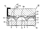
以下、本発明の第1実施形態の焦点可変レンズ装置について添付図面を参照して説明する。図1は焦点可変レンズ装置1を示している。図1(a)は本発明の焦点可変レンズ装置1を示す平面図であり、図1(b)は図1(a)をA−A'断面で下方から見た断面図であり、図1(c)は図1(a)をB−B'断面で左方から見た断面図である。
【0015】
焦点可変レンズ装置1は、第1の基板に相当するシリコンなどの半導体からなる基板2と第2の基板に相当するガラスなどの光透過性を有する基板3の2層からなり、シリコン基板2とガラス基板3は後述するレンズ用穴4と溝7を除くシリコン基板2とガラス基板3とが接する面で陽極接合などにより接着されている。
【0016】
シリコン基板2にはシリコン基板2を厚み方向に貫通するように第1の穴に相当するレンズ用穴4とレンズ用穴4を囲むような第2の穴に相当するドーナツ形状のポンプ用穴5が開けられている。このときシリコン基板2のガラス基板3と接合されていない側から見たときのレンズ用穴4の面積とポンプ用穴5の面積とを比較すると、レンズ用穴4の面積よりもポンプ用穴5の面積の方が大きくなるように開けられていることがわかる。レンズ用穴4の周囲とポンプ用穴5の内側の周囲の間はシリコン基板2とガラス基板3が接合されている側に設けられた溝7で連通している。この溝7はレンズ用穴4の周囲全体とポンプ用穴5の内側の周囲全体に設けられていても良いし、所定の間隔を持って複数設けられていても良い。
【0017】
シリコン基板2においてガラス基板3と接合されていない側にシリコンなどの半導体からなり、光透過性を有する膜状の弾性部材に相当する弾性膜6が形成されている。この弾性膜6はレンズ用穴4とポンプ用穴5を一体的に覆うように形成されているが、便宜上レンズ用穴4を覆う箇所を6a、ポンプ用穴5を覆う箇所を6bと呼ぶ。
【0018】
そして、ガラス基板3、レンズ用穴4、ポンプ用穴5、溝7と弾性膜6とで形成される閉じた空間には変形可能な光透過性物質に相当する純水8やシリコンオイルなどの流動性の高い物質が封入されており、レンズ用穴4、弾性膜6a、純水8が一体となってレンズとして作用する。また、弾性膜6bは後述するアクチュエータ13の可動電極として作用する。
【0019】
この弾性膜6はポンプ用穴5の周囲の内側と外側においてシリコン基板2と対向しない側に向けてそれぞれ凸部14を有しており、外側の凸部14上の所定の箇所に弾性膜6bと導通している可動電極用パッド9が形成され、さらにその2箇所の凸部14上で可動電極用パッド9や可動電極用パッド9に電気的に接続される図示しない配線を形成した箇所以外の箇所に形成された窒化膜などの絶縁層11を介して支持される導電性の固定電極10がポンプ用穴5を覆うように形成されている。この凸部14により弾性膜6bと固定電極10は所定の距離を保つことができる。さらに絶縁層11上に固定電極10と導通するように固定電極用パッド12を形成する。そして固定電極用パッド12と可動電極用パッド9の間に電圧を印加することにより弾性膜6bと固定電極10の間に電位差が発生し、その結果、弾性膜6bと固定電極10の間に静電力が発生して弾性膜6bが吸引されるので、弾性膜6bと固定電極10は静電アクチュエータ13として作用する。
【0020】
弾性膜6bが吸引されると、ガラス基板3、ポンプ用穴5、弾性膜6bで形成される空間の体積が大きくなり、純水8が溝7を通じて流入する。その結果、シリコン基板2,レンズ用穴4,弾性膜6aで形成される空間の体積が小さくなり、すなわちレンズの厚さが薄くなりレンズの焦点距離が長くなる。静電アクチュエータ13に電圧印加をやめると弾性膜6bが元に戻り、純水8が溝7を通じて再度シリコン基板2,レンズ用穴4,弾性膜6aで形成される空間に流入しレンズの厚さが厚くなる。
【0021】
このように、静電アクチュエータ13へ印加する電圧に応じて、ガラス基板3、ポンプ用穴5、弾性膜6bで形成される空間の体積が変化してポンプとして作用する。
【0022】
なお、本実施例では弾性膜6は一体的に形成されているが、弾性膜6aと弾性膜6bを異なる材料で形成しても良い。これにより、例えば、弾性膜6aは可動電極として作用しないため導電性に関係なく光透過性に優れた材料を用い、弾性膜6bはレンズとして作用しないため光透過性に関係なく導電性を有しかつ弾性が優れた材料を用いることができる。よって、弾性膜6aと6bで必要とされる特性に合わせて最適な材料を選択することができる。
【0023】
次に本発明の第1実施形態の焦点可変レンズ装置の製造方法について添付図面を参照して説明する。図2は焦点可変レンズ装置1の製造プロセスを示している。なお、第1実施形態と同じ機能を有する構成要素については第1実施形態と同一の符号を用いる。
【0024】
図2(a)において、P型シリコンからなるシリコン基板2の上面全体に熱酸化膜17を成膜する。そしてフォトリソグラフィにより熱酸化膜17をパターニングし、水酸基を有する硝酸でウェットエッチングをするか、もしくはドライエッチングを行って固定電極10を支持する凸部14となる凹部及びレンズとして作用する凹部を形成する。
【0025】
図2(b)において、熱酸化膜17を除去した後、イオン注入法、拡散法などにより不純物をシリコン基板2にドーピングし、シリコン基板2の上面全体にN型シリコンからなる弾性膜6を形成する。
【0026】
図2(c)において、弾性膜6の上のうち可動電極用パッド9や可動電極用パッド9に電気的に接続される図示しない配線を形成する箇所にだけレジストを設け、その後弾性膜6の上全体にCVD法などにより絶縁層11となる窒化膜を成膜し、窒化膜が成膜されない部分には酸化膜18を形成する。
【0027】
図2(d)において、弾性膜6aとして作用する箇所の窒化膜および可動電極用パッド9や可動電極用パッド9に電気的に接続される図示しない配線を形成する箇所に設けたレジストを除去した後、絶縁層11が形成された凸部14上にCVD法などでドーナツ形状のポリシリコン膜19を形成し、パターニングする。
【0028】
図2(e)において、ポリシリコン膜19にイオン注入法、拡散法などにより不純物をドーピングして固定電極10となる低抵抗層を形成する。さらにシリコン基板2の裏面に図示しない酸化膜を形成し、パターニングを行ってエッチングし、溝7を形成する。
【0029】
図2(f)において、シリコン基板2の裏面全体に窒化膜20を成膜し、パターニングする。さらにECE法(Electoro Chemical Etching)や時間制御エッチングなどで円錐台形状(断面が台形形状になっているすり鉢状)のレンズ用穴4と断面が台形形状であるドーナツ形状のポンプ用穴5を形成する。
【0030】
図2(g)において、不要となった窒化膜を除去した後、PVD法やCVD法などでアルミなどの金属を成膜することにより、固定電極10に電気的に接続される図示しない配線とそれに繋がる固定電極用パッド12、及び弾性膜6bに電気的に接続される図示しない配線とそれに繋がる可動電極用パッド9を形成する。
【0031】
図2(h)において、純水8を注入するための貫通穴15を設けたガラス基板3をシリコン基板2におけるレンズ用穴4と溝7を形成した側のレンズ用穴4と溝7以外の面で陽極接合により接合する。なお貫通穴はガラス基板3、レンズ用穴4,ポンプ用穴5、弾性膜6,溝7で形成される空間と連通するように設けられている。
【0032】
図2(i)において、ガラス基板3の貫通穴から純水8を弾性膜6が膨らみ破壊されない程度に注入し、ガラス基板3のシリコン基板2との接合面と反対面全体を光透過性を有する封止樹脂16などでコーティングし純水8を封止する。
このように本実施例による焦点可変レンズ装置においては、半導体の製造プロセスにより製作することができるので、従来の焦点可変レンズ装置に比較して装置全体を小型にすることができる。
【0033】
次に本発明の第2実施形態の焦点可変レンズ装置について添付図面を参照して説明する。図3は第2実施形態の焦点可変レンズ装置30の断面図を示している。第1実施形態と同じ機能を有する構成要素については第1実施形態と同一の符号を用いる。
【0034】
本実施形態においてはシリコン基板2に形成された弾性膜6のシリコン基板2と反対側に絶縁層11を介してガラスなどの光透過性を有する第3の基板に相当する電極用基板21を接合している。電極用基板21には接合前に予めCVD法などにより固定電極10、固定電極用パッド12、その他の配線を形成してあるので、静電アクチュエータ13を含む焦点可変レンズ装置全体の製作を容易にすることができる。
【0035】
次に本発明の第3実施形態の焦点可変レンズ装置について添付図面を参照して説明する。図4は第3実施形態の焦点可変レンズ装置40の断面図を示している。ここでも、第1実施形態、第2実施形態と同じ機能を有する構成要素については第1実施形態、第2実施形態と同一の符号を用いる。
【0036】
本実施形態においては、ガラス基板3においてレンズ用穴4に対向する箇所に所望の曲率を有する凹部に相当する非球面状凹部22を形成している。この非球面状凹部22はシリコン基板2とガラス基板3を接合する前にエッチング法や研磨法により予め形成されている。
【0037】
レンズ用穴4を覆う弾性膜6により形成されるレンズは球面を有するので平行光が入射した場合に球面収差が発生するが、その収差を補正するように非球面状凹部22を非球面状に加工することにより収差を吸収し、球面収差の発生をなくすることができる。
【0038】
なお、第3実施形態は上記第2実施形態のように電極用基板21を用いるような焦点可変レンズ装置30に対しても適用することができる。
【0039】
【発明の効果】
請求項1の発明による焦点可変レンズ装置においては、半導体の製造プロセスにより製作することができるので、従来の焦点可変レンズ装置に比較して装置全体を小型にすることができる。
【0040】
請求項2の発明による焦点可変レンズ装置においても、半導体の製造プロセスにより製作することができるので、従来の焦点可変レンズ装置に比較して装置全体を小型にすることができる。さらに第1の穴と第2の穴を覆う弾性部材を別々にしたので、各々必要な特性に対して最適な特性を有する弾性部材を使用することができる。
【0041】
又、請求項1又は2の発明による焦点可変レンズ装置においては、請求項1または2より装置全体を小型化にできたためレンズの焦点を可変させるために必要な力が小さくてすむ。よって、電磁力方式や圧電方式に比べて発生トルクの小さい静電アクチュエータで装置を駆動させることができる。よって、装置全体の消費電力を減少させることができる。
【0042】
請求項3の発明による焦点可変レンズ装置においては、レンズの焦点を可変させるために使用する静電アクチュエータの固定電極や固定電極に通電するための固定電極用パッドを予め第3の基板上に形成することができるので、静電アクチュエータを含む焦点可変レンズ装置全体の製作を容易にすることができる。
【0043】
請求項4の発明による焦点可変レンズ装置においては、パスカルの原理により、レンズの焦点距離を可変させるために第2の穴を覆う弾性部材に印加する力をレンズ、すなわち第1の穴を覆う弾性部材を直接変形させる力と比較して小さくすることができ、小さなトルクのアクチュエータで焦点距離を変えることができる。
【0044】
請求項5の発明による焦点可変レンズ装置においては、第1の穴を覆う弾性部材により形成されるレンズは球面を有するので平行光が入射した場合に球面収差が発生するが、その収差を補正するように凹部を非球面に加工することにより収差を吸収し、球面収差を発生させることなく所望の焦点を有する焦点可変レンズ装置を実現することができる。
【0045】
請求項6の発明による焦点可変レンズ装置においては、第1の穴と第2の穴の間の光透過性物質の流入、流出がスムーズに行われるのでレンズ変形の高速応答性を得ることができる。
【0046】
請求項7の発明による焦点可変レンズ装置においては、複数の溝以外の箇所では第1の基板と第2の基板は接合されているので、第1の穴の剛性が高くなり外部から引火される振動や衝撃に対してもレンズが変形せず、焦点距離を安定して維持することができる。
【図面の簡単な説明】
【図1】本発明の第1の実施形態を示す図である。
【図2】本発明の第1の実施形態の製造プロセスを示す図である。
【図3】本発明の第2の実施形態を示す図である。
【図4】本発明の第3の実施形態を示す図である。
【符号の説明】
1 第1実施形態の焦点可変レンズ装置
2 シリコン基板
3 ガラス基板
4 レンズ用穴
5 ポンプ用穴
6 弾性膜
6a 弾性膜6の内レンズ用穴4を覆う箇所
6b 弾性膜6の内ポンプ用穴5を覆う箇所
7 溝
8 純水
9 可動電極用パッド
10 固定電極
11 絶縁層
12 固定電極用パッド
13 静電アクチュエータ
14 凸部
15 貫通穴
16 封止樹脂
17 熱酸化膜
18 酸化膜
19 ポリシリコン膜
20 窒化膜
21 電極用基板
22 非球面状凹部
30 第2実施形態の焦点可変レンズ装置
40 第3実施形態の焦点可変レンズ装置[0001]
BACKGROUND OF THE INVENTION
The present invention relates to a variable focus lens device.
[0002]
[Prior art]
Conventionally, in the variable focus lens device, the refractive index of the lens is changed using liquid crystal or the like, or the lens itself is moved by an actuator to change the focus. In addition, those in which liquid is sealed in the lens can be found in Japanese Patent Application Laid-Open Nos. 7-49404 and 10-269599. In either case, the lens thickness is changed by an external drive source to change the focal length.
[0003]
[Problems to be solved by the invention]
However, since these drive sources are driven by an electromagnetic force method or a piezoelectric method, the entire lens apparatus cannot be reduced in size and power consumption is large. Furthermore, in Japanese Patent Laid-Open No. 7-49404, the amount of liquid in the lens unit is changed in order to change the thickness of the lens, but the inflow or outflow direction of liquid when changing the amount of liquid in the lens unit is the same. Because of the direction, it took a long time until the amount of liquid changed to form a uniform lens shape, that is, until it functioned correctly as a lens, and the high-speed response was low.
[0004]
In Japanese Patent Laid-Open No. 10-269599, since the thickness of the lens is changed without changing the amount of liquid inside, the variable amount of thickness is small and the variable focal distance is also small.
[0005]
The present invention has been made in view of such circumstances, and an object of the present invention is to provide a compact variable focus lens device using a semiconductor process.
[0006]
[Means for Solving the Problems]
In the invention of
[0007]
In the invention of
[0009]
According to a third aspect of the present invention, the elastic member according to the first aspect or the second elastic member according to the second aspect is disposed on a side of the first substrate on which the second substrate is not disposed. A third substrate having light transmissivity is disposed, and the fixed electrode is formed on the third substrate.
[0010]
According to a fourth aspect of the present invention, the area of the second hole viewed from the side of the first substrate where the second substrate is not disposed is larger than the area of the first hole. .
[0011]
The invention according to
[0012]
According to a sixth aspect of the present invention, the first hole and the second hole communicate with each other through a groove provided between the entire periphery of the first hole and the entire periphery inside the second hole. It is characterized by that.
[0013]
In the invention of
[0014]
DETAILED DESCRIPTION OF THE INVENTION
Hereinafter, a variable focus lens device according to a first embodiment of the present invention will be described with reference to the accompanying drawings. FIG. 1 shows a variable
[0015]
The variable
[0016]
The
[0017]
On the side of the
[0018]
The closed space formed by the
[0019]
The
[0020]
When the
[0021]
Thus, according to the voltage applied to the
[0022]
In this embodiment, the
[0023]
Next, a method of manufacturing the variable focus lens device according to the first embodiment of the present invention will be described with reference to the accompanying drawings. FIG. 2 shows a manufacturing process of the variable
[0024]
In FIG. 2A, a thermal oxide film 17 is formed on the entire upper surface of the
[0025]
In FIG. 2B, after the thermal oxide film 17 is removed, an impurity is doped into the
[0026]
In FIG. 2C, a resist is provided only on the
[0027]
In FIG. 2 (d), the resist provided in the portion where the nitride film acting as the
[0028]
In FIG. 2E, a low resistance layer to be the fixed
[0029]
In FIG. 2F, a
[0030]
In FIG. 2G, after removing the unnecessary nitride film, a metal such as aluminum is formed by a PVD method, a CVD method or the like, thereby forming a wiring (not shown) electrically connected to the fixed
[0031]
In FIG. 2 (h), the
[0032]
In FIG. 2 (i),
As described above, the variable focus lens device according to the present embodiment can be manufactured by a semiconductor manufacturing process, so that the entire device can be made smaller than a conventional variable focus lens device.
[0033]
Next, a variable focus lens apparatus according to a second embodiment of the present invention will be described with reference to the accompanying drawings. FIG. 3 shows a cross-sectional view of the variable
[0034]
In this embodiment the
[0035]
Next, a variable focus lens apparatus according to a third embodiment of the present invention will be described with reference to the accompanying drawings. FIG. 4 shows a sectional view of the variable
[0036]
In the present embodiment, an aspherical
[0037]
Since the lens formed by the
[0038]
The third embodiment can also be applied to the variable
[0039]
【The invention's effect】
Since the variable focus lens device according to the first aspect of the present invention can be manufactured by a semiconductor manufacturing process, the entire device can be made smaller than the conventional variable focus lens device.
[0040]
Since the variable focus lens device according to the second aspect of the present invention can also be manufactured by a semiconductor manufacturing process, the entire device can be reduced in size as compared with the conventional variable focus lens device. Furthermore, since the elastic member covering the first hole and the second hole is separated, it is possible to use an elastic member having an optimum characteristic for each necessary characteristic.
[0041]
In the variable focus lens device according to the first or second aspect of the invention, the force required to change the focal point of the lens can be reduced because the entire device can be made smaller than in the first or second aspect. Therefore, the apparatus can be driven by an electrostatic actuator that generates less torque than the electromagnetic force method or the piezoelectric method. Therefore, the power consumption of the entire apparatus can be reduced.
[0042]
In the variable focus lens device according to the invention of
[0043]
In the variable focus lens apparatus according to the fourth aspect of the present invention, the force applied to the elastic member that covers the second hole in order to vary the focal length of the lens in accordance with Pascal's principle is the elasticity that covers the lens, that is, the first hole. The force can be reduced as compared with the force that directly deforms the member, and the focal length can be changed with a small torque actuator.
[0044]
In the variable focus lens device according to the fifth aspect of the present invention, since the lens formed by the elastic member covering the first hole has a spherical surface, spherical aberration occurs when parallel light enters, but the aberration is corrected. Thus, by processing the concave portion into an aspherical surface, it is possible to realize a variable focus lens device having a desired focus without absorbing the aberration and generating the spherical aberration.
[0045]
In the variable focus lens device according to the sixth aspect of the invention, since the inflow and outflow of the light transmitting material between the first hole and the second hole are smoothly performed, high-speed response of lens deformation can be obtained. .
[0046]
In the variable focus lens device according to the seventh aspect of the invention, since the first substrate and the second substrate are joined at places other than the plurality of grooves, the rigidity of the first hole is increased and the first substrate is ignited from the outside. The lens is not deformed by vibration or shock, and the focal length can be stably maintained.
[Brief description of the drawings]
FIG. 1 is a diagram showing a first embodiment of the present invention.
FIG. 2 is a diagram showing a manufacturing process according to the first embodiment of the present invention.
FIG. 3 is a diagram showing a second embodiment of the present invention.
FIG. 4 is a diagram showing a third embodiment of the present invention.
[Explanation of symbols]
DESCRIPTION OF
Claims (7)
前記第1の基板には前記第1の基板と前記第2の基板が接着されている側から前記第1の基板を厚み方向にエッチングによって円形の第1の穴と第2の穴が開けられており、
前記第1の穴と前記第2の穴は前記第1の基板と前記第2の基板が接着されている側で連通しており、
前記第1の基板における前記第2の基板が接着されていない側の表面は前記第1の穴と前記第2の穴を一体的に覆うように前記第1の基板に不純物をドーピングして形成した光透過性と導電性を有する膜状の弾性部材となっており、
前記第1の基板と前記第2の基板と前記弾性部材で形成される空間に変形可能な光透過性物質が封入されており、
前記弾性部材のうち前記第2の穴に対向する箇所であってかつ前記第1の基板と反対側にポリシリコン膜に不純物をドーピングした固定電極が形成されており、
前記弾性部材と前記固定電極との間に電圧を印加することにより、前記弾性部材のうち前記第2の穴を覆う箇所が静電力により前記固定電極に吸引される可動電極として作用する静電アクチュエータを構成し、
レンズとして作用する前記第1の穴を囲むように前記第2の穴がドーナツ形状に配置されていること、
を特徴とする焦点可変レンズ装置。Wherein the first substrate made of silicon first substrate opposite to a second substrate having optical transparency that is against wear,
In the first substrate, circular first holes and second holes are formed by etching the first substrate in the thickness direction from the side where the first substrate and the second substrate are bonded. And
It said first bore and said second bore is in communication with said first substrate and said second side board that are against wear,
Surface of said first side contact Keru the second substrate to the substrate is not adhered impurities are doped into the first substrate to cover the second hole and the first hole integrally has a film-like elastic member having optical transparency and conductivity formed Te,
A deformable light-transmitting substance is enclosed in a space formed by the first substrate, the second substrate, and the elastic member,
A fixed electrode doped with an impurity in a polysilicon film is formed on the elastic member at a position facing the second hole and on the side opposite to the first substrate,
By applying a voltage between the elastic member and the fixed electrode, the electrostatic that the elastic portion cormorants covering the second hole of the member acts as a movable electrode is attracted to the fixed electrode by an electrostatic force Configure the actuator,
Said second hole is located in a donut shape so as to surround the first hole, which acts as a lens,
A variable focus lens device characterized by the above.
前記第1の基板には前記第1の基板と前記第2の基板が接着されている側から前記第1の基板の厚み方向にエッチングによって円形の第1の穴と第2の穴が開けられており、
前記第1の穴と前記第2の穴は前記第1の基板と前記第2の基板が接着されている側で連通しており、
前記第1の基板における前記第2の基板が接着されていない側の表面は前記第1の穴を覆うように前記第1の基板に不純物をドーピングして形成した光透過性を有する膜状の第1の弾性部材となっており、
さらに前記第1の基板における前記第2の基板が接着されていない側の表面は前記第2の穴を覆うように前記第1の基板に不純物をドーピングして形成した導電性を有する膜状の第2の弾性部材となっており、
前記第1の基板と前記第2の基板と前記第1の弾性部材と前記第2の弾性部材で形成される空間に変形可能な光透過性物質が封入されており、
前記弾性部材のうち前記第2の穴に対向する箇所であってかつ前記第1の基板と反対側にポリシリコン膜に不純物をドーピングした固定電極が形成されており、
前記弾性部材と前記固定電極との間に電圧を印加することにより、前記弾性部材のうち前記第2の穴を覆う箇所が静電力により前記固定電極に吸引される可動電極として作用する静電アクチュエータを構成し、
レンズとして作用する前記第1の穴を囲むように前記第2の穴がドーナツ形状に配置されていること、
を特徴とする焦点可変レンズ装置。Comprising: a first substrate made of silicon, the second substrate having the first substrate opposite to the light-transmitting that are against wear,
Circular first and second holes are formed in the first substrate by etching in the thickness direction of the first substrate from the side where the first substrate and the second substrate are bonded. And
It said first bore and said second bore is in communication with said first substrate and said second side board that are against wear,
The film surface of said first side contact Keru the second substrate to the substrate is not adhered having optical transparency formed by doping impurity into the first substrate to cover the first hole A first elastic member having a shape,
Further, the surface of the first side contact Keru the second substrate to the substrate is not adhered film having conductivity formed by doping impurity into the first substrate to cover the second hole Jo of has a second elastic member,
A deformable light transmissive substance is enclosed in a space formed by the first substrate, the second substrate, the first elastic member, and the second elastic member,
A fixed electrode doped with an impurity in a polysilicon film is formed on the elastic member at a position facing the second hole and on the side opposite to the first substrate,
By applying a voltage between the elastic member and the fixed electrode, a portion of the elastic member that covers the second hole acts as a movable electrode that is attracted to the fixed electrode by electrostatic force. Configure
The second hole is arranged in a donut shape so as to surround the first hole acting as a lens;
A variable focus lens device characterized by the above.
前記第1の基板において前記第2の基板が配置されていない側に請求項1に記載の前記弾性部材または請求項2に記載の前記第2の弾性部材を介して光透過性を有する第3の基板が配置され、前記固定電極は前記第3の基板上に形成されていること、
を特徴とする焦点可変レンズ装置。The variable focus lens apparatus according to claim 1 or 2,
The elastic member or the optical transparency and through the second elastic member according to claim 2 according to claim 1 on a side where the second substrate on the first substrate is not disposed third is the substrate of the arrangement, Rukoto the fixed electrode is formed on the third substrate having,
A variable focus lens device characterized by the above.
前記第1の基板の前記第2の基板が配置されていない側から見た前記第2の穴の面積は前記第1の穴の面積より大きいこと、
を特徴とする焦点可変レンズ装置。The variable focus lens apparatus according to claim 1 or 2 ,
The area of the second hole viewed from the side where the second substrate of the first substrate is not disposed is larger than the area of the first hole ;
A variable focus lens device characterized by the above.
前記第2の基板の前記第1の基板と接する側に前記第1の穴と同心で所望の曲率を有する凹部を設けたこと、
を特徴とする焦点可変レンズ装置。The variable focus lens apparatus according to claim 1 or 2,
A concave portion having a desired curvature concentric with the first hole is provided on a side of the second substrate in contact with the first substrate;
A variable focus lens device characterized by the above.
前記第1の穴と前記第2の穴とは前記第1の穴の周囲全体と前記第2の穴の内側の周囲全体との間に設けられた溝で連通していること、
を特徴とする焦点可変レンズ装置。The variable focus lens apparatus according to claim 1 or 2,
The first hole and the second hole communicate with each other by a groove provided between the entire periphery of the first hole and the entire periphery inside the second hole ;
A variable focus lens device characterized by the above.
前記第1の穴と前記第2の穴とは前記第1の穴の周囲から前記第2の穴に向かって設けられた複数の溝で連通していること、
を特徴とする焦点可変レンズ装置。The variable focus lens apparatus according to claim 1 or 2,
The first hole and the second hole communicate with each other through a plurality of grooves provided from the periphery of the first hole toward the second hole;
A variable focus lens device characterized by the above.
Priority Applications (1)
| Application Number | Priority Date | Filing Date | Title |
|---|---|---|---|
| JP2001309361A JP3687585B2 (en) | 2001-10-05 | 2001-10-05 | Variable focus lens device |
Applications Claiming Priority (1)
| Application Number | Priority Date | Filing Date | Title |
|---|---|---|---|
| JP2001309361A JP3687585B2 (en) | 2001-10-05 | 2001-10-05 | Variable focus lens device |
Publications (2)
| Publication Number | Publication Date |
|---|---|
| JP2003114309A JP2003114309A (en) | 2003-04-18 |
| JP3687585B2 true JP3687585B2 (en) | 2005-08-24 |
Family
ID=19128523
Family Applications (1)
| Application Number | Title | Priority Date | Filing Date |
|---|---|---|---|
| JP2001309361A Expired - Fee Related JP3687585B2 (en) | 2001-10-05 | 2001-10-05 | Variable focus lens device |
Country Status (1)
| Country | Link |
|---|---|
| JP (1) | JP3687585B2 (en) |
Families Citing this family (11)
| Publication number | Priority date | Publication date | Assignee | Title |
|---|---|---|---|---|
| JP5069232B2 (en) * | 2005-07-25 | 2012-11-07 | カール・ツァイス・エスエムティー・ゲーエムベーハー | Projection objective lens of microlithography projection exposure apparatus |
| JP4760426B2 (en) * | 2006-02-13 | 2011-08-31 | ソニー株式会社 | Optical element and lens array |
| US7715107B2 (en) * | 2006-04-25 | 2010-05-11 | Asml Netherlands B.V. | Optical element for correction of aberration, and a lithographic apparatus comprising same |
| KR20080043106A (en) | 2006-11-13 | 2008-05-16 | 삼성전자주식회사 | Optical lens and manufacturing method thereof |
| FR2919074B1 (en) * | 2007-07-19 | 2010-10-22 | Commissariat Energie Atomique | OPTICAL DEVICE WITH MEMBRANE DEFORMABLE BY ELECTROSTATIC ACTUATION |
| FR2919073B1 (en) * | 2007-07-19 | 2010-10-15 | Commissariat Energie Atomique | OPTICAL DEVICE WITH MEANS FOR ACTUATING A COMPACT DEFORMABLE MEMBRANE |
| EP2034338A1 (en) * | 2007-08-11 | 2009-03-11 | ETH Zurich | Liquid Lens System |
| EP2239600A1 (en) | 2010-06-02 | 2010-10-13 | Optotune AG | Adjustable optical lens |
| EP2612065B1 (en) | 2010-09-02 | 2017-05-17 | Optotune AG | Illumination source with variable divergence |
| KR20130139952A (en) | 2010-10-26 | 2013-12-23 | 옵토투네 아게 | Variable focus lens having two liquid chambers |
| DE102013209823B4 (en) * | 2013-05-27 | 2015-10-08 | Fraunhofer-Gesellschaft zur Förderung der angewandten Forschung e.V. | Optical structure with webs disposed thereon and method of making the same |
-
2001
- 2001-10-05 JP JP2001309361A patent/JP3687585B2/en not_active Expired - Fee Related
Also Published As
| Publication number | Publication date |
|---|---|
| JP2003114309A (en) | 2003-04-18 |
Similar Documents
| Publication | Publication Date | Title |
|---|---|---|
| US7580195B2 (en) | Optical lens and method of manufacturing the same | |
| JP3687585B2 (en) | Variable focus lens device | |
| EP2074445B1 (en) | Method for manufacturing adjustable lens | |
| KR101403676B1 (en) | Optical Lens and Manufacturing Method Thereof | |
| JP2010504555A (en) | Small polymer lens | |
| US20100079873A1 (en) | Package structure of liquid lens | |
| JP2009186935A (en) | Variable-focus liquid lens and method of manufacturing the same | |
| US7679811B2 (en) | Image system and miniature deformable mirror thereof | |
| US8004771B2 (en) | Varifocal lens and method of manufacturing the same | |
| JP2002357774A (en) | Varifocal optical element | |
| CN111880257A (en) | Adjustable optical filter device | |
| US11392008B2 (en) | Liquid lens | |
| KR101675108B1 (en) | Varifocal lens and method for manufacturing the same | |
| JP3577693B2 (en) | Micro movable device and manufacturing method thereof | |
| CN214335449U (en) | Optical micro-electro-mechanical device and micro-projector apparatus | |
| US10996432B2 (en) | Reflective active variable lens and method of fabricating the same | |
| US20230062685A1 (en) | Varaiable focal length optical element | |
| CN112995448A (en) | Imaging module and manufacturing method thereof | |
| CN115373129A (en) | Variable focus lens, method of forming the same, and electronic apparatus | |
| CN114609772A (en) | Lens, lens module, camera assembly and electronic equipment | |
| KR0177227B1 (en) | Method for fabricating a module of an optical projection system | |
| CN114981701A (en) | Adjustable optical filter device | |
| JP2001013426A (en) | Manufacture of light modulation device | |
| KR20080038627A (en) | Liquid lens module |
Legal Events
| Date | Code | Title | Description |
|---|---|---|---|
| A131 | Notification of reasons for refusal |
Free format text: JAPANESE INTERMEDIATE CODE: A131 Effective date: 20050208 |
|
| A521 | Written amendment |
Free format text: JAPANESE INTERMEDIATE CODE: A523 Effective date: 20050411 |
|
| TRDD | Decision of grant or rejection written | ||
| A01 | Written decision to grant a patent or to grant a registration (utility model) |
Free format text: JAPANESE INTERMEDIATE CODE: A01 Effective date: 20050517 |
|
| A61 | First payment of annual fees (during grant procedure) |
Free format text: JAPANESE INTERMEDIATE CODE: A61 Effective date: 20050530 |
|
| R150 | Certificate of patent or registration of utility model |
Free format text: JAPANESE INTERMEDIATE CODE: R150 |
|
| FPAY | Renewal fee payment (event date is renewal date of database) |
Free format text: PAYMENT UNTIL: 20080617 Year of fee payment: 3 |
|
| FPAY | Renewal fee payment (event date is renewal date of database) |
Free format text: PAYMENT UNTIL: 20090617 Year of fee payment: 4 |
|
| LAPS | Cancellation because of no payment of annual fees |