JP3680763B2 - Data transfer control device and electronic device - Google Patents
Data transfer control device and electronic device Download PDFInfo
- Publication number
- JP3680763B2 JP3680763B2 JP2001143430A JP2001143430A JP3680763B2 JP 3680763 B2 JP3680763 B2 JP 3680763B2 JP 2001143430 A JP2001143430 A JP 2001143430A JP 2001143430 A JP2001143430 A JP 2001143430A JP 3680763 B2 JP3680763 B2 JP 3680763B2
- Authority
- JP
- Japan
- Prior art keywords
- information
- storage area
- data
- transferred
- data transfer
- Prior art date
- Legal status (The legal status is an assumption and is not a legal conclusion. Google has not performed a legal analysis and makes no representation as to the accuracy of the status listed.)
- Expired - Lifetime
Links
Images


Classifications
-
- G—PHYSICS
- G06—COMPUTING; CALCULATING OR COUNTING
- G06F—ELECTRIC DIGITAL DATA PROCESSING
- G06F13/00—Interconnection of, or transfer of information or other signals between, memories, input/output devices or central processing units
-
- G—PHYSICS
- G06—COMPUTING; CALCULATING OR COUNTING
- G06F—ELECTRIC DIGITAL DATA PROCESSING
- G06F5/00—Methods or arrangements for data conversion without changing the order or content of the data handled
- G06F5/06—Methods or arrangements for data conversion without changing the order or content of the data handled for changing the speed of data flow, i.e. speed regularising or timing, e.g. delay lines, FIFO buffers; over- or underrun control therefor
- G06F5/10—Methods or arrangements for data conversion without changing the order or content of the data handled for changing the speed of data flow, i.e. speed regularising or timing, e.g. delay lines, FIFO buffers; over- or underrun control therefor having a sequence of storage locations each being individually accessible for both enqueue and dequeue operations, e.g. using random access memory
Landscapes
- Engineering & Computer Science (AREA)
- Theoretical Computer Science (AREA)
- Physics & Mathematics (AREA)
- General Engineering & Computer Science (AREA)
- General Physics & Mathematics (AREA)
- Information Transfer Systems (AREA)
- Communication Control (AREA)
Abstract
Description
【0001】
【発明の属する技術分野】
本発明は、データ転送制御装置及び電子機器に関する。
【0002】
【背景技術及び発明が解決しようとする課題】
近年、パーソナルコンピュータと周辺機器(広義には電子機器)とを接続するためのインターフェース規格として、USB(Universal Serial Bus)が注目を集めている。このUSBには、従来は別々の規格のコネクタで接続されていたマウスやキーボードやプリンタなどの周辺機器を、同じ規格のコネクタで接続できると共にいわゆるプラグ&プレイやホットプラグも実現できるという利点がある。
【0003】
一方、このUSBには、同じくシリアルバスインターフェース規格として脚光を浴びているIEEE1394に比べて、転送速度が遅いという問題点がある。
【0004】
そこで、従来のUSB1.1の規格に対する互換性を持ちながら、USB1.1に比べて格段に高速な480Mbps(HSモード)のデータ転送速度を実現できるUSB2.0規格が策定され、注目を浴びている。
【0005】
さて、このUSB2.0では、HS(High Speed)モード時には480Mbpsでデータ転送が行われる。従って、高速な転送速度が要求されるハードディスクドライブや光ディスクドライブなどのストレージ機器のインターフェースとして用いることができるという利点がある。
【0006】
しかしながら、その一方で、USBバスに接続されるデータ転送制御装置は、480Mbpsという高速で転送されてくるデータを処理しなければならない。従って、データ転送制御装置の処理速度や、データ転送制御装置を制御するファームウェア(CPU)の処理速度が遅いと、実効的な転送速度を確保できず、バス帯域をロスしてしまうという課題がある。
【0007】
本発明は、以上のような技術的課題に鑑みてなされたものであり、その目的とするところは、実効的なバスの転送速度を向上できるデータ転送制御装置及び電子機器を提供することにある。
【0008】
【課題を解決するための手段】
上記課題を解決するために本発明は、バスを介したデータ転送のためのデータ転送制御装置であって、1つのエンドポイントを介して転送される情報として第1、第2の情報を含む複数種類の情報が割り当てられている場合に、第1の情報用の第1の記憶領域と第2の情報用の第2の記憶領域とが1つのエンドポイントに対応して用意されるバッファと、バスを介して第1の情報が転送される第1のフェーズでは、エンドポイントからホストに向けて転送される情報を、第1の情報用の前記第1の記憶領域から読み出し、バスを介して第2の情報が転送される第2のフェーズでは、エンドポイントからホストに向けて転送される情報を、第2の情報用の前記第2の記憶領域から読み出すバッファ管理回路とを含むことを特徴とする。
【0009】
本発明によれば、所与のエンドポイントに割り当てられる第1の情報用の第1の記憶領域と、同じエンドポイントに割り当てられる第2の情報用の第2の記憶領域とが、バッファに用意される。そして、第1のフェーズ(第1のトランスポート)では、エンドポイントからホストに向けて転送される情報が第1の記憶領域から読み出され、第2のフェーズ(第2のトランスポート)では、エンドポイントからホストに向けて転送される情報が第2の記憶領域から読み出される。
【0010】
このようにすれば、1つのエンドポイントに複数種類の情報が割り当てられている場合にも、第1の記憶領域から第1の情報を読み出す処理を行っている間に、第2の記憶領域の第2の情報についての処理を行うことが可能になる。従って、第1のフェーズから第2のフェーズに移行した場合に、第2のフェーズでの第2の情報についての処理を早期に完了させることが可能になり、実効的なバスの転送速度を向上できる。
【0011】
また本発明は、第1の情報用に用意された前記第1の記憶領域が、先に入力された情報が先に出力される領域に設定され、第2の情報用に用意された前記第2の記憶領域が、ランダムアクセス可能な領域に設定されることを特徴とする。
【0012】
このようにすれば、第2の記憶領域に書き込まれた第2の情報についての処理を効率化でき、実効的なバスの転送速度を向上できる。
【0013】
また本発明は、前記第1の情報が、データのパケットであり、前記第2の情報が、ステータスブロックのパケットであることを特徴とする。
【0014】
但し、本発明においては、第1、第2の記憶領域に記憶される第1、第2の情報の種類は任意に設定できる。
【0015】
また本発明は、データのパケットが前記第1の記憶領域から読み出されている間に、前記第2の記憶領域のステータスブロックのパケットが用意されることを特徴とする。
【0016】
このようにすれば、第1のフェーズから第2のフェーズに移行した場合に、第2の記憶領域から第2の情報を読み出す処理等を早期に開始できるようになり、実効的なバスの転送速度を向上できる。
【0017】
また本発明は、前記第2の記憶領域が、成功ステータス用の第1のステータスブロックのパケットが書き込まれる第3の記憶領域と、不成功ステータス用の第2のステータスブロックのパケットが書き込まれる第4の記憶領域を含み、成功ステータスの場合には、成功ステータス用の前記第1のステータスブロックのパケットが前記第3の記憶領域から読み出され、不成功ステータスの場合には、不成功ステータス用の前記第2のステータスブロックのパケットが前記第4の記憶領域から読み出されることを特徴とする。
【0018】
このようにすれば、不成功ステータスが生じない限り、情報の読み出し領域を第3の記憶領域に固定できるようになるため、領域の切り替え処理などの負荷を軽減できる。
【0019】
また本発明は、前記第3の記憶領域には、成功ステータス用のデフォルト情報が設定されたステータスブロックのパケットが予め書き込まれることを特徴とする。
【0020】
このようにすれば、デフォルト情報の部分についての情報の更新処理を省略できるようになるため、第2の情報についての処理の負荷を軽減できる。
【0021】
また本発明は、デフォルト情報が設定されたステータスブロックのパケットの情報のうち、ステータスブロックのパケットとコマンドブロックのパケットとを関連づけるためのタグ情報が更新され、更新後のステータスブロックのパケットが、前記第1のステータスブロックのパケットとして前記第3の記憶領域から読み出されることを特徴とする。
【0022】
このようにすれば、タグ情報等の更新(書き換え、上書き)だけを行えば済むようになるため、第2の情報についての処理の負荷を更に軽減できる。
【0023】
また本発明は、前記第1のフェーズから前記第2のフェーズに切り替わったと判断された場合に、エンドポイントからホストに向けて転送される情報の読み出し領域が、前記第1の記憶領域から前記第2の記憶領域に切り替えられることを特徴とする。
【0024】
このようにすれば、フェーズ切り替えを判断するだけで、情報の読み出し領域を切り替えることが可能になり、データ転送制御装置の処理負荷を軽減できる。
【0025】
また本発明は、第2のバスを介して前記第1の情報を転送して前記第1の記憶領域に書き込む転送処理が終了し、且つ、前記第1の記憶領域が空になったことを条件に、前記第1のフェーズから前記第2のフェーズに切り替わったと判断されることを特徴とする。
【0026】
このようにすれば、簡素な回路制御と回路構成で、フェーズ切り替えを判断できるようになり、データ転送制御装置のコンパクト化、低コスト化を図れる。
【0027】
また本発明は、バスを介したデータ転送のためのデータ転送制御装置であって、1つのエンドポイントを介して転送される情報としてデータのパケットとステータスブロックのパケットとが割り当てられている場合に、データ用のデータ記憶領域とステータスブロック用のステータス記憶領域とが1つのエンドポイントに対応して用意されるバッファと、バスを介してデータのパケットが転送されるデータフェーズから、バスを介してステータスブロックのパケットが転送されるステータスフェーズに切り替わった場合に、情報の読み出し領域をデータ用の前記データ記憶領域からステータスブロック用のステータス記憶領域に切り替え、エンドポイントからホストに向けて転送されるステータスブロックのパケットを前記ステータス記憶領域から読み出すバッファ管理回路とを含むことを特徴とする。
【0028】
本発明によれば、所与のエンドポイントに割り当てられるデータパケット用のデータ記憶領域と、同じエンドポイントに割り当てられるステータスブロックパケット用のステータス記憶領域とが、バッファに用意される。そして、データフェーズ(データトランスポート)からステータスフェーズ(ステータストランスポート)に切り替わった場合に、ホストに向けて転送される情報の読み出し領域が、データ記憶領域からステータス記憶領域に切り替わる。
【0029】
このようにすることで、1つのエンドポイントにデータパケットとステータスブロックパケットとが割り当てられている場合にも、データ記憶領域からデータパケットを読み出す処理を行いながら、ステータスブロックパケットについての処理を行うことが可能になる。従って、データ転送制御装置の処理速度の向上や、ステータスブロックパケットを処理する手段の負荷を軽減することが可能になり、実効的なバスの転送速度を向上できる。
【0030】
また本発明は、USB(Universal Serial Bus)の規格に準拠したデータ転送を行うことを特徴とする。
【0031】
但し、本発明はUSB以外の規格(USBの思想を受け継ぐ規格)に準拠したデータ転送に適用することも可能である。
【0032】
また本発明に係る電子機器は、上記のいずれかのデータ転送制御装置と、前記データ転送制御装置及びバスを介して転送されるデータの出力処理又は取り込み処理又は記憶処理を行う装置とを含むことを特徴とする。
【0033】
本発明によれば、データ転送制御装置のデータ転送を制御する処理手段(ファームウェア等)の処理負荷を軽減できるため、電子機器の低コスト化、小規模化などを図れる。また、本発明によれば、高速な転送モードでデータ転送を行うことも可能になるため、電子機器の処理の高速化を図れる。
【0034】
【発明の実施の形態】
以下、本実施形態について図面を用いて詳細に説明する。
【0035】
なお、以下に説明する本実施形態は、特許請求の範囲に記載された本発明の内容を何ら限定するものではない。また本実施形態で説明される構成の全てが本発明の解決手段として必須であるとは限らない。
【0036】
1.USB
1.1 データ転送手法
まず、USB(USB2.0)のデータ転送手法について簡単に説明する。
【0037】
USBでは、IEEE1394等とは異なり、データ転送の主導権をホストが有している。即ち、データ転送のトランザクションを起動するのはホスト側であり、データ転送に関する大部分の制御はホストが行う。このため、ホストの処理負荷は重くなるが、ホストとなるPC(パーソナルコンピュータ)等は高速で高性能なCPU(プロセッサ)を有しているため、このように負荷の重い処理もそれほど問題にはならない。
【0038】
一方、USBにおいては、デバイス(ターゲット)はホストからの要求に対して単に応えるだけでよいため、デバイス側の処理、構成については簡素化できる。従って、デバイス側ではホストのような高性能で高速なCPUを使用する必要が無く、低価格なCPU(マイコン)を使用できるようになり、低コスト化を図れる。
【0039】
さて、USBではこのようなホスト主導のデータ転送を実現するために、図1(A)に示すようなエンドポイント(EP0〜15)がデバイス側に用意される。ここで、エンドポイントは、ホストとデバイスとの間でデータ転送を行うためのバッファ(FIFO)の入り口に相当するものであり、USBでのデータ転送は、全て、このエンドポイントを経由して行われる。
【0040】
そして、このエンドポイントは、デバイスアドレスとエンドポイント番号により一義的にアドレス指定できるようになっている。即ちホストは、デバイスアドレスとエンドポイント番号を指定することで、所望のエンドポイントへのデータ送信や、所望のエンドポイントからのデータ受信を自由に行うことができる。
【0041】
また、エンドポイントの設定はデバイス側の任意であり、エンドポイント番号の割り当てや、各エンドポイントに割り当てられる記憶領域のデータサイズ等は、エニミュレーション(enumeration)処理時にホストは知ることができる。
【0042】
なお、USBにおいては、データ転送のタイプとして、コントロール転送、アイソクロナス転送、インタラプト転送、バルク転送が用意されている。
【0043】
ここで、コントロール転送は、ホストとデバイス(ターゲット)との間でコントロールエンドポイントを介して行われる制御用の転送モードである。このコントロール転送により、デバイスの初期化のためのコンフィグレーション情報等が転送される。
【0044】
アイソクロナス転送は、画像データや音声データのように、データの正当性よりもバンド幅の確保が優先されるデータの転送のために用意された転送モードである。このアイソクロナス転送では、一定周期に一定量のデータを転送できることが保証されるため、データのリアルタイム性が重要なアプリケーションに有効な転送モードとなる。
【0045】
インタラプト転送は、比較的低い転送速度で少量のデータを転送するために用意された転送モードである。
【0046】
バルク転送は、不定期に発生する大量のデータを転送するために用意された転送モードである。このバルク転送では、アイソクロナス転送やインタラプト転送により使用された時間以外の空いた時間においてデータ転送が行われると共に、データの正当性がチェックされる。従って、リアルタイム性はあまり重要ではないが、データの信頼性は確保したいデータの転送に有効な転送モードである。
【0047】
1.2 トランザクション構成
さて、図1(B)に示すように、USBのバルク転送におけるトランザクションは基本的に、トークンパケット、データパケット、ハンドシェークパケットという3つのパケットにより構成される。なお、アイソクロナス転送の場合は、ハンドシェークパケットは不要になる。
【0048】
ここでトークンパケットは、ホストがデバイス(ターゲット)のエンドポイントのリードやライトを要求する場合等に使用されるパケットである。このトークンパケットは、例えば、PID(OUT、IN、SOF、SETUPなどのパケットID)、ADDR(デバイスアドレス)、ENDP(エンドポイント番号)、CRC(Cyclic Redundancy Check)のフィールドを有する。
【0049】
また、データパケットは、データの実体を送るためのパケットであり、PID(DATA0、DATA1)、DATA(データの実体)、CRCのフィールドを有する。
【0050】
また、ハンドシェークパケットは、データ受信に成功したか否かを受信側が送信側に伝えるためのパケットであり、PID(ACK、NAK、STALL)のフィールドを有する。
【0051】
OUTトランザクション(ホストがデバイスに情報を出力するトランザクション)では、図1(C)に示すように、まず、ホストがデバイスに対してOUTトークンパケットを転送する。次に、ホストはデバイスに対してOUTのデータパケットを転送する。そして、デバイスは、OUTのデータパケットの受信に成功すると、ホストに対してACKのハンドシェークパケットを転送する。
【0052】
一方、INトランザクション(ホストがデバイスから情報を入力するトランザクション)では、図1(D)に示すように、まず、ホストがデバイスに対してINトークンパケットを転送する。そして、INトークンパケットを受信したデバイスは、ホストに対してINのデータパケットを転送する。そして、ホストは、INのデータパケットの受信に成功すると、デバイスに対してACKのハンドシェークパケットを転送する。
【0053】
なお、図1(C)、(D)において、”D←H”は、ホストからデバイスに対して情報が転送されることを意味し、”D→H”は、デバイスからホストに対して情報が転送されることを意味する(以下の説明及び図でも同様)。
【0054】
1.3 Bulk−Only
さて、USBのデバイスは種々のクラスに分類される。そして、ハードディスクドライブや光ディスクドライブなどのデバイスは、マスストレージと呼ばれるクラスに属し、このマスストレージクラスには、電子機器のベンダ等により作成されたCBI(Control/Bulk/Interrupt)やBulk−Onlyなどの仕様がある。
【0055】
そして、CBI仕様では図2(A)に示すように、デバイスは、コントロール、バルクアウト、バルクイン、インタラプトのエンドポイントEP0、1、2、3を用意する。ここで、エンドポイントEP0では、USB層のコントロールのパケットや、コマンドのパケットが転送される。また、EP1ではOUTデータ(ホストからデバイスに転送されるデータ)、EP2ではINデータ(デバイスからホストに転送されるデータ)、EP3ではインタラプトINのパケットが転送される。なお、EP1〜15のいずれを、バルクアウト、バルクイン、インタラプトINのエンドポイントに割り当てるかは、デバイス側の任意である。
【0056】
一方、Bulk−Only仕様では図2(B)に示すように、デバイスは、コントロール、バルクアウト、バルクインのエンドポイントEP0、1、2を用意する。ここで、エンドポイントEP0では、USB層のコントロールのパケットが転送される。また、EP1ではコマンド(CBW)及びOUTデータ、EP2ではステータス(CSW)及びINデータのパケットが転送される。なお、EP1〜15のいずれを、バルクアウト、バルクインのエンドポイントに設定するかは、デバイス側の任意である。
【0057】
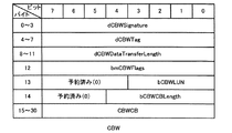
ここで、CBW(Command Block Wrapper)は、コマンドブロック及びこれに関連する情報を含むパケットであり、図3にそのフォーマットが示される。また、CSW(Command Status Wrapper)は、コマンドブロックのステータスを含むパケットであり、図4にそのフォーマットが示される。
【0058】
図3において、dCBWSignatureは、当該パケットをCBWとして識別するための情報であり、dCBWTagは、コマンドブロックのタグであり、dCBWDataTransferLengthはデータフェーズにおいて転送されるデータの長さを指定する。また、bmCBWFlagsは転送方向等を指定するためのフラグであり、dCBWLUNはロジカルユニット番号であり、bCBWCBLengthはコマンド長であり、CBWCBは、ATA/ATAPIやSCSIなどのコマンドがカプセル化されて記述されるコマンドブロックである。
【0059】
また図4において、dCSWSignatureは、当該パケットをCSWとして識別するための情報である。また、dCSWTagは、ステータスブロックのタグであり、当該CSWに対応するCBWのdCBWTagの値が書き込まれる。また、CSWDataResidueは、CBWのdCBWDataTransferLengthにより指定されたデータの長さとデバイスが実際に処理したデータの長さの差であり、bCSWStatusはステータスブロックである。
【0060】
次に、図2(B)のBulk−Only仕様におけるデータの書き込み処理、読み出し処理について、図5(A)、(B)を用いて説明する。
【0061】
ホストがデバイスにデータを書き込む場合には、図5(A)に示すように、まず、ホストがCBWをデバイスに転送するコマンドフェーズ(コマンドトランスポート)が行われる。具体的には、ホストが、エンドポイントEP1を指定するトークンパケットをデバイスに転送し、次に、CBW(図2(B)のA1、図3参照)をデバイスのエンドポイントEP1に転送する。このCBWにはライトコマンドが含まれる。そして、デバイスからホストにACKのハンドシェーク(H.S)が返却されると、コマンドフェーズが終了する。
【0062】
コマンドフェーズ(コマンドトランスポート)が終了するとデータフェーズ(データトランスポート)に移行する。このデータフェーズでは、まず、ホストが、エンドポイントEP1を指定するトークンパケットをデバイスに転送し、次に、OUTデータ(図2(B)のA2参照)をデバイスのエンドポイントEP1に転送する。そして、デバイスからホストにACKのハンドシェークが返却されると、1つのトランザクションが終了する。そして、このようなトランザクションが繰り返され、CBWのdCBWDataTransferLength(図3参照)で指定されるデータ長の分だけデータが転送されると、データフェーズが終了する。
【0063】
データフェーズ(データトランスポート)が終了するとステータスフェーズ(ステータストランスポート)に移行する。このステータスフェーズでは、まず、ホストが、エンドポイントEP2を指定するトークンパケットをデバイスに転送する。すると、デバイスが、エンドポイントEP2にあるCSW(図2(B)のA3、図4参照)をホストに転送する。そして、ホストからデバイスにACKのハンドシェークが返却されると、ステータスフェーズが終了する。
【0064】
ホストがデータを読み出す場合は、図5(B)に示すように、まず、ホストが、エンドポイントEP1を指定するトークンパケットをデバイスに転送し、次に、CBWをデバイスのエンドポイントEP1に転送する。このCBWはリードコマンドを含む。そして、デバイスからホストにACKのハンドシェークが返却されると、コマンドフェーズが終了する。
【0065】
コマンドフェーズが終了するとデータフェーズに移行する。このデータフェーズでは、まず、ホストが、エンドポイントEP2を指定するトークンパケットをデバイスに転送する。すると、デバイスが、エンドポイントEP2にあるINデータ(図2(B)のA4参照)をホストに転送し、ホストからデバイスにACKのハンドシェークが返却されると、1つのトランザクションが終了する。そして、このようなトランザクションが繰り返され、CBWのdCBWDataTransferLengthで指定されるデータ長の分だけデータが転送されると、データフェーズが終了する。
【0066】
データフェーズが終了するとステータスフェーズに移行する。このステータスフェーズの処理は図5(A)のデータの書き込み処理の場合と同様である。
【0067】
2.本実施形態の特徴
2.1 領域切り替え
さて、図2(A)に示すCBI仕様では、ホストが一定期間毎にトークンをデバイスに転送する仕様になっている。このため、ホストの処理負荷や、このトークンを受けるデバイスの処理負荷が重くなってしまうという欠点がある。
【0068】
このため、現在では、図2(B)のBulk−Only仕様が主流になってきている。
【0069】
ところが、このBulk−Only仕様では、1つのエンドポイントを介して転送される情報として、複数種類の情報が割り当てられている。具体的には、図2(B)では、バルクアウトエンドポイントEP1を介して転送される情報として、コマンド(CBW)及びOUTデータが割り当てられ、バルクインエンドポイントEP2を介して転送される情報として、ステータス(CSW)及びINデータが割り当てられている。従って、ホスト及びデバイスは、各エンドポイントを介して転送される情報がどの情報なのかを判別する必要があり、Bulk−Only仕様では、現在のフェーズがどのフェーズなのかをホスト及びデバイスが判断して、この情報の判別を行っている。
【0070】
例えば、図5(A)、(B)のB1、B2では、現在のフェーズがコマンドフェーズであるため、エンドポイントEP1を介して転送される情報はCBW(コマンド)であると判断される。また、B3、B4では、現在のフェーズがデータフェーズであるため、エンドポイントEP1を介して転送される情報はOUTデータであると判断され、エンドポイントEP2を介して転送される情報はINデータであると判断される。また、B5、B6では、現在のフェーズがステータスフェーズであるため、エンドポイントEP2を介して転送される情報はCSW(ステータス)であると判断される。
【0071】
そして、Bulk−Only仕様ではホストとデバイスとの間で常にフェーズが一致するようにデータ転送が行われるため、1つのエンドポイントに対して複数の情報(CBWとOUTデータ、CSWとINデータ)が割り当てられている場合にも、適正なデータ転送が可能になる。
【0072】
ところが、Bulk−Only仕様には、次のような問題があることが判明した。
【0073】
例えば図6(A)〜(D)に本実施形態の比較例の手法を示す。この比較例では、図6(A)に示すように、データフェーズにおいて、エンドポイントEP2を入り口とするFIFO(EP2)602に対して、ハードディスクドライブHDD等のデバイスからのデータが書き込まれる。具体的には、HDDからの読み出しデータがEBUS(第2のバス。後述する図12参照)を介してFIFO602にDMA転送される。
【0074】
そして、EBUSを介したDMA転送が終了すると、図6(B)に示すように、FIFO602が空になるのを待つ(エンプティ信号がアクティブになるのを待つ)。
【0075】
次に、FIFO602が空になり、データフェーズからステータスフェーズに移行すると、図6(C)に示すように、CPU(ファームウェア、処理手段)等が、EBUSを介したデータ転送(IDEのデータ転送)のステータスをハードディスクドライブHDD(EBUS)側から取得する。そして、取得したステータスに基づき作成したCSW(図4参照)をFIFO602に書き込む。この場合、この比較例では、CPUによるCSWの書き込み処理が終了するまでは、ホストからのINトークンに対してINのデータパケットを返すことができず、NAKを返すことになる。
【0076】
次に、図6(D)に示すように、この書き込まれたCSWが、先入れ先出し方式でFIFO602から読み出され、USBを介してホストに転送される。
【0077】
このように、この比較例では、データ(INデータ)とCSWを共通のFIFO602を用いて転送しているため、CSWの書き込み処理の終了が遅れてしまい、その分だけ実効的なデータ転送速度が低下してしまうという問題がある。
【0078】
具体的には、まず第1に、この比較例では図6(B)に示すように、FIFO602が空になるまでFIFO602へのCSWの書き込み処理を開始できない。例えば、FIFO602に499バイトのデータが残っている状態で、13バイトのCSW(図4参照)がFIFO602に書き込まれたとする。すると、FIFO602に存在するデータの量が、499+13=512バイト=最大パケットサイズになってしまい、ステータスであるCSWが、データとしてホストに転送されてしまう事態が生じてしまう。
【0079】
このため、この比較例では、FIFO602が空になるのを待ち、データフェーズからステータスフェーズに移行した後に、FIFO602にCSWを書き込む必要がある。従って、その待ち時間の分だけ、CSWの書き込み処理の終了が遅れてしまい、実効的なデータ転送速度が低下してしまう。
【0080】
また、この比較例では図6(C)に示すように、データフェーズの期間ではCSWをFIFO602に書き込むことができず、ステータスフェーズに移行した後にCSWを書き込むことになる。そして、このCSWの書き込みが終了するまでは、ホストからのINトークンに対してNAKを返すことになり、その期間の分だけ実効的なデータ転送速度が低下してしまう。
【0081】
この場合に、USB1.1ではバスの転送速度が低かったため、図6(B)、(C)に示すようなデバイス側の処理の遅れは、ほとんど問題にならなかった。
【0082】
ところが、USB2.0のHSモードでは高速な480Mbpsでデータ転送が行われる。従って、デバイス側の処理が遅れてしまうと、USB2.0の高速転送が阻害されてしまい、システム全体の実効的なデータ転送速度が大幅に低下してしまう。
【0083】
特に、デバイス側では、低コスト化の要請から、例えば20〜50MHz程度のクロック周波数で動作する安価なCPUが使用される場合が多い。従って、図6(B)、(C)の処理に非常に時間を費やしてしまい、実効的なデータ転送速度の遅れは更に深刻なものになる。
【0084】
そこで本実施形態では、このような問題を解決するために、フェーズ(トランスポート)の切り替えに応じてバッファの記憶領域を切り替える手法を採用している。
【0085】
より具体的には図7(A)に示すように本実施形態では、INデータ(第1の情報)を読み出すためのEP2領域14(第1の記憶領域。データ記憶領域)の他に、CSW(第2の情報。ステータスブロック)を読み出すためのCSW領域16(第2の記憶領域。ステータス記憶領域)を、パケット格納手段であるバッファ上に用意する。
【0086】
ここで、EP2領域14及びCSW領域16は共にバルクインのエンドポイントEP2を入り口とする記憶領域である。また、EP2領域14は、先に入力された情報が先に出力されるように設定(FIFO設定)されており、CSW領域16は、情報のランダムアクセスが可能になるように設定(ランダムアクセス設定)されている。
【0087】
そして本実施形態では図7(A)に示すように、データフェーズ(第1のフェーズ)においてはスイッチSW(切り替え手段)がEP2領域14側に切り替えられており、ホストに向けて転送されるデータ(ハードディスクHDDからのデータ)は、EP2領域14から読み出される。
【0088】
そして、EBUS(第2のバス)でのデータ転送が終了すると、図7(B)に示すように、CPU(ファームウェア、処理手段)等が、EBUSを介したデータ転送のステータスをハードディスクドライブHDD側から取得し、取得したステータスに基づきCSWを作成し、作成したCSW(図4参照)をCSW領域16に書き込む。即ち、本実施形態では、INデータのパケットがEP2領域14(第1の記憶領域)から読み出されるデータフェーズ(第1のフェーズ)の期間において、CSWを作成(準備)したり、CSWの書き込みを開始できる。また、CSW領域16はランダムアクセス可能に設定されているため、CPUは、CSW領域16の任意のアドレスに情報を高速に書き込むことができる。
【0089】
そして、EP2領域14が空になり(エンプティ信号がアクティブになり)、データフェーズ(第1のフェーズ)からステータスフェーズ(第2のフェーズ)に切り替わると、図7(C)に示すように、スイッチSW(切り替え手段)がEP2領域14側からCSW領域16側に切り替わる。これにより、CSW領域16に書き込まれたCSW(ステータスブロックのパケット)が、USB(第1のバス)を介してホストに転送されることになる。
【0090】
例えば図6(C)、(D)の比較例では、FIFO602が空になり、データフェーズからステータスフェーズに移行した後でないと、FIFO602にCSWを書き込むことができなかった。そして、このCSWの書き込みが終了するまでは、ホストのINトークンに対してNAKを返さざるを得なかった。
【0091】
これに対して本実施形態では図7(B)に示すように、データフェーズの期間に、CSWを用意し、CSW領域16に書き込むことができる。従って、図7(C)に示すように、データフェーズからステータスフェーズに移行した後、早い段階で、ホストからのINトークンに対してデータパケット(CSW)を返すことが可能になり、処理の高速化を図れる。
【0092】
特にUSB2.0では、ホストに対してデータを高速に転送できる。従って、図6(C)の比較例のようにホストからのINトークンに対してNAKを返し続けると、バス帯域がロスしてしまい、USB2.0の高速データ転送を活用できない。
【0093】
これに対して本実施形態では、図7(C)に示すようにホストからのINトークンに対して早い段階でデータパケット(CSW)を返すことが可能になる。従って、バス帯域のロスを最小限に抑えることができ、USB2.0の高速データ転送を生かすことができるため、実効的なデータ転送速度を向上できる。
【0094】
なお、本実施形態では図7(A)〜(C)に示すように、CSW領域16はランダムアクセス可能な領域に設定されているため、CSWの書き込み処理を早期に終了できる。従って、早い段階で、ホストからのINトークンに対してデータパケット(CSW)を返すことが可能になり、処理の高速化を図れる。
【0095】
一方、ハードディスクドライブHDD等からのデータを効率良くDMA転送するためには、EP2領域14については、情報が先入れ先出しされる領域に設定(FIFO設定)することが望ましい。この場合、EP2領域14を、直列接続のレジスタ、メモリ等で構成することで、先入れ先出しの領域に設定してもよいし、後述するようにRAMのアドレス制御を工夫することで、先入れ先出しの領域に設定してもよい。
【0096】
2.2 成功ステータス用の記憶領域
本実施形態では、図8(A)に示すように、CSW領域(第2の記憶領域)として、成功ステータス用のCSW0(第1のステータスブロックパケット)が書き込まれるCSW0領域18(第3の記憶領域)と、不成功ステータス用のCSW1(第2のステータスブロックパケット)が書き込まれるCSW1領域19(第4の記憶領域)とを、バッファに用意している。
【0097】
即ち、EBUS(第2のバス。図12参照)を介したデータ転送のステータスが成功ステータスの場合には、図8(A)に示すようにSW2(切り替え手段)をCSW0領域18側に接続し、成功ステータス用のCSW0をCSW0領域18から読み出して、ホストに転送する。
【0098】
一方、EBUSを介したデータ転送のステータスが不成功ステータスの場合には、図8(B)に示すようにSW2(切り替え手段)をCSW1領域19側に接続し、不成功ステータス用のCSW1をCSW1領域19から読み出して、ホストに転送する。
【0099】
一般的に、データ転送にエラーが生じる確率は非常に低い。従って、通常は、SW2をCSW0領域18側に接続しておき、成功ステータス用のCSW0をホストに転送するようにする。
【0100】
そして、データ転送にエラーが生じた場合にだけ、SW2をCSW1領域19側に接続し、エラーに応じた不成功ステータス用のCSW1をホストに転送するようにする。
【0101】
このようにすれば、EBUSでのデータ転送にエラーが生じない限り、SW2を切り替える必要がなくなる。そして、データ転送にエラーが生じる確率は極めて低いため、SW2を切り替える頻度も極めて低くなる。従って、SW2を切り替える処理等を行うCPU(ファームウェア)の処理負荷を軽減できるようになる。
【0102】
また本実施形態では、図9(A)に示すように、成功ステータス用のデフォルト情報が設定されたステータスブロックのパケットDEFCSW0を、CSW0領域18に予め書き込んでおく。そして、データ転送のステータスが成功の場合には、このDEFCSW0を用いて得られるCSW0をCSW0領域18から読み出し、ホストに転送する。
【0103】
具体的には、この成功ステータス用のDEFCSW0では、dCSWSignatureやdCSWDataResidueやbCSWStatusが、デフォルト値(例えば53425355h、00000000h、00h=goodstatus)に設定されている。そして、dCSWTag(ステータスブロックのパケットとコマンドブロックのパケットとを関連づけるためのタグ情報)は、例えばCBWの受け付け時にCBWのdCBWTagを用いて更新(上書き、書き換え)される。即ち、CBWのdCBWTagの値がdCSWTagにそのまま書き込まれる。
【0104】
このように、成功ステータス用のデフォルト情報が設定されたDEFCSW0を、CSW0領域18に予め書き込んでおけば、CPU(ファームウェア)は例えばdCSWTagを更新する作業だけを行えばよくなる。従って、CPUの処理負担を大幅に軽減でき、実効的な転送速度を向上できる。
【0105】
なお、不成功ステータス用のCSW1領域19には、図9(B)に示すようなDEFCSW1を書き込んでおく。そして、データ転送のステータスが不成功の場合には、このDEFCSW1を用いて得られるCSW1をCSW1領域19から読み出し、ホストに転送する。
【0106】
具体的には、この不成功ステータス用のDEFCSW1では、dCSWSignature等がデフォルト値に設定されている。そして、dCSWTagは、例えばCBWの受け付け時にCBWのdCBWTagを用いて更新される。また、bCSWStatusは、EBUSを介して取得したステータスを用いて更新される。このようにすることで、エラーの発生時におけるCPUの処理負荷を軽減できる。
【0107】
2.3 フェーズ切り替え
さて、本実施形態では、フェーズが切り替わったことを条件に、情報の読み出し領域の切り替えを行っている。
【0108】
具体的には図7(B)、(C)に示すように、データフェーズ(第1のフェーズ)からステータスフェーズ(第2のフェーズ)に切り替わった場合に、エンドポイントEP2からホストに向けて転送される情報(INデータ、ステータス)の読み出し領域を、EP2領域14(第1の記憶領域)からCSW領域16(第2の記憶領域。CSW0領域、CSW1領域)に切り替えている。
【0109】
このようにフェーズ切り替えを判断して情報の読み出し領域を切り替えるようにすれば、適切な領域切り替え処理を少ない処理負荷で実現できるようになる。
【0110】
この場合のフェーズ切り替えの判断は、具体的には以下のように行う。
【0111】
例えばホストからデバイスにOUTデータが転送される場合(第1の方向のデータ転送の場合)には、図10のようにしてフェーズ切り替えを判断できる。即ち、図10のG1に示すように、ハードディスクドライブHDD等に接続されるEBUS(第2のバス。図12参照)を介したデータ転送(DMA転送)が終了したタイミングで、データフェーズからステータスフェーズに切り替わったと判断する。このG1のタイミングは、USBでのデータ転送(データフェーズ)が終了するG2のタイミングよりも遅いタイミングとなる。また、このG1のタイミングは、EP1領域(OUTデータの記憶領域)が空になり、Empty信号がアクティブになるG3のタイミングと一致する。そして、このG1のタイミングは、EBUS側に設けられたカウンタ(図12のDMAカウンタ82)を用いて、EBUSで転送されるデータサイズ(転送数。データ長)をカウントすることで判断できる。
【0112】
一方、デバイスからホストにINデータが転送される場合(第2の方向のデータ転送の場合)には、図11のようにしてフェーズ切り替えを判断できる。即ち、図11のG4に示すように、EBUSを介したデータ転送(第2のバスを介して第1の記憶領域に第1の情報が書き込まれる転送処理)が終了したと判断された後、G5に示すように、EP2領域(INデータの記憶領域。第1の記憶領域)が空になり、Empty信号がアクティブになったタイミングで、データフェーズからステータスフェーズに切り替わったと判断する。この場合、G4のタイミングは、EBUS側に設けられたカウンタ(DMAカウンタ82)を用いて、EBUSで転送されるデータサイズをカウントすることで判断できる。また、G5のタイミングは、USBでのデータ転送が終了するG6のタイミングと一致する。
【0113】
図10、図11の手法によりフェーズ切り替えを判断すれば、EBUS(第2のバス)側にだけカウンタ(DMAカウンタ82)を設ければよく、USB(第1のバス)側にカウンタを設ける必要がなくなる。従って、回路制御を容易化できると共に回路構成を簡素化でき、データ転送制御装置のコンパクト化、低コスト化を図れる。
【0114】
そして本実施形態では、図11のG5のタイミングでデータフェーズからステータスフェーズに切り替わったと判断し、このタイミングで、図7(B)、(C)に示すようにEP2領域14からCSW領域16への切り替え処理を行っている。このようにすれば、EBUS側のカウンタ(DMAカウンタ82)のカウント値とEmpty信号をモニタするだけで、情報の読み出し領域を切り替えることが可能になるため、少ない処理負荷で領域の切り替え処理を実現できるようになる。
【0115】
2.4 構成例
図12に本実施形態のデータ転送制御装置の構成例を示す。
【0116】
本実施形態のデータ転送制御装置は、トランシーバマクロ20、SIE30、エンドポイント管理回路40、バッファ管理回路50、バッファ60、バルク転送管理回路70、DMAC80を含む。なお、本発明のデータ転送制御装置は、図12に示す回路ブロックの全てを含む必要はなく、それらの一部を省略する構成としてもよい。
【0117】
ここで、トランシーバマクロ20は、USB(第1のバス)のFSモードやHSモードでのデータ転送を実現するための回路である。このトランシーバマクロ20としては、例えばUSB2.0の物理層回路や、論理層回路の一部についてのインターフェースを定義したUTMI(USB2.0 Transceiver Macrocell Interface)に準拠したマクロセルを用いることができる。このトランシーバマクロ20は、トランシーバ回路22、クロック生成回路24を含む。
【0118】
トランシーバ回路22は、差動信号DP、DMを用いてUSB(第1のバス)上のデータを送受信するアナログフロントエンド回路(受信回路、送信回路)を含む。また、ビットスタッフィング、ビットアンスタッフィング、シリアル・パラレル変換、パラレル・シリアル変換、NRZIデコード、NRZIエンコード、サンプリングクロック生成などの処理を行う回路を含む。
【0119】
またクロック生成回路24は、データ転送制御装置が使用する動作クロックや、サンプリングクロックの生成に使用されるクロックなどを生成する回路であり、480MHzや60MHzのクロックを生成するPLLや発振回路などを含む。
【0120】
SIE(Serial Interface Engine)は、USBのパケット転送処理などの種々の処理を行う回路であり、パケットハンドラ回路32、サスペンド&レジューム制御回路34、トランザクション管理回路36を含む。
【0121】
パケットハンドラ回路32は、ヘッダ及びデータからなるパケットの組み立て(生成)や分解などを行う回路であり、CRCの生成や解読を行うCRC処理回路33を含む。
【0122】
サスペンド&レジューム制御回路34は、サスペンドやレジューム時のシーケンス制御を行う回路である。
【0123】
トランザクション管理回路36は、トークン、データ、ハンドシェークなどのパケットにより構成されるトランザクションを管理する回路である。具体的には、トークンパケットを受信した場合には、自分宛か否かを確認し、自分宛の場合には、ホストとの間でデータパケットの転送処理を行い、その後に、ハンドシェークパケットの転送処理を行う。
【0124】
エンドポイント管理回路40は、バッファ60の各記憶領域の入り口となるエンドポイントを管理する回路であり、エンドポイントの属性情報を記憶するレジスタ(レジスタセット)などを含む。
【0125】
バッファ管理回路50は、例えばRAMなどで構成されるバッファ60を管理する回路である。より具体的には、書き込みアドレスや読み出しアドレスを生成し、バッファ60へのデータの書き込み処理やバッファ60からのデータの読み出し処理を行う。
【0126】
バッファ60(パケット記憶手段)は、USBを介して転送されるデータ(パケット)を一時的に記憶するものであり、USB(第1のバス)でのデータ転送速度と、EBUS(第2のバス)でのデータ転送速度との速度差を補償する機能などを有する。なお、EBUSは、ハードディスクドライブやCDドライブなどのデバイス(マスストレージデバイス)に接続される外部バスである。
【0127】
そして本実施形態では、1つのエンドポイントを介して転送される情報として複数種類の情報が割り当てられている場合に、第1の情報(例えばデータ)用の第1の記憶領域(例えばデータ記憶領域)と第2の情報(例えばステータスブロック)用の第2の記憶領域(例えばステータス記憶領域)とが、このバッファ60上に用意(確保)される。
【0128】
バルク転送管理回路70は、USBにおけるバルク転送を管理するための回路である。
【0129】
DMAC80は、EBUSを介してDMA転送を行うためのDMAコントローラであり、DMAカウンタ82を含む。そしてDMAカウンタ82は、EBUSを介して転送されるデータのサイズ(転送数)をカウントする回路である。
【0130】
2.5 詳細な構成例
図13に、トランザクション管理回路36(SIE)、エンドポイント管理回路40、バッファ管理回路50、バッファ60の詳細な構成例を示す。
【0131】
バッファ60(RAM)は、エンドポイントEP2に割り当てられた情報であるCSW(ステータスブロック)を記憶するCSW0領域61(成功ステータス用)、CSW1領域62(不成功ステータス用)、EP0に割り当てられた情報であるコントロールを記憶するEP0領域63、EP1に割り当てられた情報であるOUTデータを記憶するEP1領域64、EP2に割り当てられた情報であるINデータを記憶するEP2領域65を含む。
【0132】
そして図13では、CSW0領域61、CSW1領域62については、CPU(ファームウェア、処理手段)によるランダムアクセスが可能になるように設定されている。一方、EP0、EP1、EP2領域63、64、65は、先に入力された情報が先に出力されるように設定(FIFO設定)されている。
【0133】
トランザクション管理回路36は、USBを介して転送される書き込みデータSIEWrData(書き込みパケット)をバッファ60に出力し、読み出しデータSIERdData(読み出しパケット)をバッファ60から入力する。
【0134】
またトランザクション管理回路36は、バッファ管理回路50に対して書き込み要求信号SIEWrReq、読み出し要求信号SIERdReqを出力し、バッファ管理回路50から書き込みアクノリッジ信号SIEWrAck、読み出しアクノリッジ信号SIERdAckを受ける。
【0135】
またトランザクション管理回路36は、エンドポイント管理回路40に対して、トランザクション終了信号TranEndPulse、トランザクションステータス信号TranStatus、エンドポイント番号指定信号EPnum、転送方向指定信号Directionを出力し、エンドポイント管理回路40から、エンドポイント存在信号EPexistを受ける。
【0136】
エンドポイント管理回路40は、エンドポイントの属性情報(エンドポイント番号、最大パケットサイズ等)を記述するためのレジスタ(レジスタセット)42、43、44を含む。そして、トランザクション管理回路36からの各種信号と、レジスタの属性情報とに基づいて、エンドポイント選択信号EPselを生成して、バッファ管理回路50に出力する。
【0137】
またエンドポイント管理回路40は、バッファ管理回路50に対して、CPUからの書き込み要求信号CPUWrReq、読み出し要求信号CPURdReqを出力し、バッファ管理回路50から、CPUへの書き込みアクノリッジ信号CPUWrAck、読み出しアクノリッジ信号CPURdAckを受ける。
【0138】
エンドポイント管理回路40が含むEP0レジスタ42は、USB仕様によりデフォルトで定義されるコントロールエンドポイントの属性情報を記述するためのレジスタである。
【0139】
またEP1、EP2レジスタ43、44は、BULK−Only仕様により定義されるバルクアウトやバルクインのエンドポイントの属性情報を記述するためのレジスタである。なお、エンドポイントEP1〜15のいずれを、バルクアウト又はバルクインのエンドポイントに設定するかはデバイス側の任意である。
【0140】
EP1レジスタ43では、データの転送方向を表すフラグDIRがOUTに設定されており、EP1はバルクアウトのエンドポイントに設定されている。
【0141】
また、EP1レジスタ43では、フラグEnCSWが0に設定されている。このEnCSWは、エンドポイントをバッファ60のCSW0領域61又はCSW1領域62に接続するためのフラグであり、EnCSWが1に設定されるバルクインのエンドポイントはCSW0領域61又はCSW1領域62に接続されることになる。
【0142】
また、EP1レジスタ43では、フラグSelCSWが0に設定されている。このSelCSWは、CSW0領域61とCSW1領域62のいずれにバルクインのエンドポイントを接続するかを選択するためのフラグである。例えば、EnCSWが1に設定され、SelCSWが0に設定されるバルクインのエンドポイントは、CSW0領域61に接続されることになる。一方、EnCSWが1に設定され、SelCSWが1に設定されるバルクインのエンドポイントは、CSW1領域62に接続されることになる
EP2レジスタ44では、データの転送を方向を表すフラグDIRがINに設定されており、EP2はバルクインのエンドポイントに設定されている。
【0143】
また、EP2レジスタ44では、EnCSWが1に設定され、SelCSWが0に設定されている。従って、この設定状態においては、エンドポイントEP2は、CSW0領域61に接続されることになる。この場合に例えば、SelCSWを1に設定すれば、エンドポイントEP2はCSW1領域62に接続され、EnCSWを0に設定すれば、EP2はEP2領域65に接続されることになる。
【0144】
バッファ管理回路50は、トランザクション管理回路36やエンドポイント管理回路40からの書き込み・読み出し要求信号や、エンドポイント管理回路40からのエンドポイント選択信号EPselを受け、アドレスAddressや書き込みパルスxWR(xは負論理を意味する)をバッファ60に出力する。このバッファ管理回路50は、CSW0、CSW1、EP0、EP1、EP2のアドレス生成回路51、52、53、54、55とセレクタ56を含む。
【0145】
ここでCSW0アドレス生成回路51は、CSW0領域61(先頭アドレスa0)についての、SIEWrData、SIERdDataの書き込み又は読み出しアドレスAD0を生成する。
【0146】
また、CSW1アドレス生成回路52は、CSW1領域62(先頭アドレスa1)についての、SIEWrData、SIERdDataの書き込み又は読み出しアドレスAD1を生成する。
【0147】
また、EP0、EP1、EP2のアドレス生成回路53、54、55は、各々、EP0、EP1、EP2の領域63、64、65(先頭アドレスa2、a3、a4)についての、SIEWrData、SIERdDataの書き込み又は読み出しアドレスAD2、AD3、AD4を生成する。具体的には、a2、a3、a4を先頭アドレスとして順次インクリメント(又はデクリメント)するアドレスAD2、AD3、AD4を生成する。
【0148】
セレクタ56は、信号EPselに基づいてアドレスAD0〜4のいずれかを選択し、Addressとしてバッファ60に出力すると共に、書き込みパルスxWRをバッファ60に出力する。具体的には、EPselによりCSW0が選択指示された場合にはAD0を選択し、CSW1が選択指示された場合にはAD1を選択し、EP0が選択指示された場合にはAD2を選択し、EP1が選択指示された場合にはAD3を選択し、EP2が選択指示された場合にはAD4を選択して、Addressとしてバッファ60に出力する。
【0149】
なお、CSW0領域61、CSW1領域62は、CPUによるCPUWrDataの書き込みが可能になっている。この場合には、バッファ管理回路50は、エンドポイント管理回路40からのEPselやCPUWrReqに基づいて、CPUWrDataの書き込みのためのAddressやxWrをバッファ60に出力することになる。
【0150】
図14に、トランザクション管理回路36、エンドポイント管理回路40、バッファ管理回路50、バッファ60の他の構成例を示す。
【0151】
図13と異なり図14では、バッファ60が、CSW(CSW0、CSW1)、EP0、EP1、EP2用のFIFO66、67、68、69(例えば直列接続されたレジスタ、メモリ)を含む。
【0152】
そしてバッファ管理回路50が含むセレクタ57は、エンドポイント管理回路40からのEPselに基づいて、トランザクション管理回路36からのSIEWrDataを、WrDataCSW、WrDataEP0、WrDataEP1、WrDataEP2のいずれかとしてバッファ60に出力する。
【0153】
或いは、セレクタ57は、EPselに基づいて、バッファ60からのRdDataCSW、RdDataEP0、RdDataEP1、RdDataEP2のいずれかを選択して、SIERdDataとしてトランザクション管理回路36に出力する。
【0154】
より具体的には、EPselによりCSWが選択指示された場合には、WrDataCSW、RdDataCSWが選択され、EP0が選択指示された場合には、WrDataEP0、RdDataEP0が選択され、EP1が選択指示された場合には、WrDataEP1、RdDataEP1が選択され、EP2が選択指示された場合には、WrDataEP2、RdDataEP2が選択されることになる。
【0155】
そして、バッファ60へのデータの書き込みは、トランザクション管理回路36からの書き込みパルスSIEWRにより行われ、バッファ60からのデータの読み出しは、トランザクション管理回路36からの読み出しパルスSIERDにより行われる。
【0156】
なお図14において、FIFO66(CSW)をランダムアクセス可能な記憶領域に設定するようにしてもよい。
【0157】
2.6 動作
図15〜図20に、本実施形態のデータ転送制御装置の詳細な動作を説明するためのタイミング波形図の例を示す。
【0158】
2.6.1 成功ステータス
図15、図16、図17は、EBUS(第2のバス)でのデータ転送のステータスが成功ステータスであった場合のタイミング波形図である。そして、図15はステータスフェーズ(成功ステータスを伝えるフェーズ)の開始時でのタイミング波形図であり、図16、図17はステータスフェーズの終了時でのタイミング波形図である。
【0159】
図15のH1、H2に示すようにトランザクション管理回路36がEPnumを2(エンドポイント番号=2)に設定し、DirectionをINに設定すると、バルクインエンドポイントEP2のレジスタ44(図13参照)が存在するため、エンドポイント管理回路40は、H3に示すようにEPexistをアクティブ(Hレベル)にする。
【0160】
この時、H4に示すようにエンドポイントEP2のEnCSWがHレベル(1)に設定されているため、エンドポイント管理回路40は、H5に示すようにCSW0領域61のアドレスAD0を選択指示するEPselを、バッファ管理回路50に対して出力する。これにより、バッファ管理回路50のセレクタ56は、CSW0アドレス生成回路51により生成されるアドレスAD0を選択するようになる。
【0161】
そして、H6に示すように、トランザクション管理回路36がSIERdReqをアクティブにすると、H7に示すように、バッファ管理回路50は、CSW0アドレス生成回路51からのAD0=a0をAddressとしてバッファ60に出力する。これにより、バッファ60のCSW0領域61のa0を先頭アドレスとして、H9に示すようにCSW0(SIERdData)の0〜3バイトが読み出される。その後、H10に示すようにSIERdAckがアクティブにされ、トランザクション管理回路36にアクノリッジを返される。
【0162】
次に、H11に示すようにトランザクション管理回路36がSIERdReqをアクティブにすると、H12に示すように、バッファ管理回路50は、AD0=a0+4をAddressとしてバッファ60に出力する。これにより、CSW0領域61のa0+4を先頭アドレスとして、H14に示すようにCSW0(SIERdData)の4〜7バイトが読み出される。その後、H15に示すようにSIERdAckがアクティブにされ、トランザクション管理回路36にアクノリッジを返される。
【0163】
以上のような読み出し処理を繰り返すことで、図16のH16に示すように、CSW0の全ての0〜12バイト(合計で13バイト)がCSW0領域61から読み出され、ホストに転送される。
【0164】
そして、H17に示すようにホストから適正なACKが返されると、H18に示すようにトランザクション管理回路36がTranEndPulseをアクティブにすると共に、H19に示すようにTranStatusをSuccessに設定して、トランザクションが成功したことをエンドポイント管理回路40に伝える。
【0165】
すると、H20に示すようにエンドポイントEP2(図13のレジスタ44)のEnCSWがLレベル(0)に設定される。これにより、H21に示すように領域切り替えが行われ、その後のデータフェーズにおいてエンドポイントEP2が選択された場合には、バッファ管理回路50のセレクタ56は、EP2領域65のアドレスAD4を、Addressとして選択するようになる。
【0166】
図17は、ステータスフェーズのトランザクションでACKフェイルが生じた場合のタイミング波形図である。
【0167】
ホストに対して転送した成功ステータスに対して、図17のI1に示すようにホストからACKが返って来なかった場合には、トランザクション管理回路36はエンドポイント管理回路40に対して、I2に示すようにACKフェイルがあったことを示すTranStatusを出力する。すると、この場合には、図16のH20の場合とは異なり、図17のI3に示すようにエンドポイントEP2のEnCSWはLレベルにならない。このため、I4に示すようにEPselも変化せず、CSW0領域61からEP2領域65への領域切り替えは行われない。
【0168】
2.6.2 不成功ステータス
図18、図19、図20は、EBUS(第2のバス)でのデータ転送のステータスが不成功ステータスであった場合のタイミング波形図である。そして、図18はステータスフェーズ(不成功ステータスを伝えるフェーズ)の開始時でのタイミング波形図であり、図19、図20はステータスフェーズの終了時でのタイミング波形図である。
【0169】
図18のJ0では図15のH0とは異なり、領域の選択信号であるSelCSW(EP2)がHレベル(1)になっており、CSW1領域62が選択されている。従って、図18のJ5では図15のH5とは異なり、エンドポイント管理回路40が、CSW1領域62のアドレスAD1を選択指示するEPselを出力する。これにより、J7に示すように、バッファ管理回路50は、CSW1アドレス生成回路52からのAD1=a1をAddressとしてバッファ60に出力することになる。
【0170】
そして、図19のJ16に示すようにCSW1の全ての0〜12バイト(合計で13バイト)がCSW1領域62から読み出され、J17に示すようにホストから適正なACKが返却されると、J18に示すようにTranEndPulseをアクティブになり、J19に示すようにSuccessのTranStatusが出力される。これにより、不成功ステータスをホストに伝えるトランザクションが成功したことがエンドポイント管理回路40に伝えられる。また、J20に示すようにEnCSW(EP2)がLレベルになり、J21に示すように領域切り替えが行われる。
【0171】
図20は、ステータスフェーズ(不成功ステータスを伝えるフェーズ)のトランザクションでACKフェイルが生じた場合のタイミング波形図である。
【0172】
ホストに対して転送した不成功ステータスに対して、図20のK1に示すようにホストからACKが返って来なかった場合には、K2に示すようにACKフェイルがあったことを示すTranStatusが出力される。すると、この場合には、図19のJ20の場合とは異なり、図20のK3に示すようにEnCSWはLレベルにならない。このため、K4に示すようにEPselも変化せず、CSW1領域62からEP2領域65への領域切り替えは行われない。
【0173】
2.7 比較例と本実施例との比較
図21(A)に比較例(図6(A)〜(D))のタイミング波形図の例を示し、図21(B)に本実施形態のタイミング波形図の例を示す。
【0174】
例えば図21(A)の比較例では、データフェーズにおいては、エンドポイントEP2のFIFOにはINデータが存在するため、CSWをFIFO(EP2)に書き込むことができない。従って、図21(A)のL1に示すように、ステータスフェーズに移行した後に、CSWの書き込み処理が開始することになる。従って、この書き込み処理が終了するまでは、L2、L3に示すようにホストからのINトークンに対してNAKを返さなければならなくなる。このため、L4に示すようにホストへのCSWの転送も遅れてしまい、L5に示すように次のコマンドフェーズへの移行も遅れてしまう。この結果、バス帯域がロスしてしまい、実効的な転送速度が低下してしまう。
【0175】
一方、図21(B)の本実施形態では、EP2領域とは別にCSW領域(CSW0領域、CSW1領域)が設けられているため、CSWを用意する処理やCSWをCSW領域に書き込む処理を、データフェーズの間に開始できる。従って、L6に示すように、ホストからのINトークンに対して初めの数回はNAKを返す可能性はあるが、L7に示すようにEnCSWがHレベルになり、EP2領域からCSW領域への切り替えが行われると、L8に示すようにCSW領域のCSWをホストに対して直ぐに転送できる。従って、図21(A)の比較例に比べて、L9に示すようにコマンドフェーズへの移行も早くなる。この結果、バス帯域のロスも最小限に抑えることができ、比較例に比べて実効的な転送速度を向上できる。
【0176】
図22(A)に比較例の場合のファームウェア(CPU)の処理のフローチャートを示し、図22(B)に本実施形態の場合のファームウェアの処理のフローチャートを示す。
【0177】
図22(A)の比較例では、ファームウェアは、まず、データフェーズが終了したか否かを判断する(ステップS21)。
【0178】
そして、データフェーズが終了したと判断した場合には、ファームウェアは、CSWをEP2用のFIFOに書き込む(ステップS22。図21(A)のL1参照)。そして、CSWは13バイトであり、最大パケットサイズよりも小さいショートパケットであるため、ショートパケットの転送をイネーブルにする(ステップS23)。
【0179】
次に、CSWをホストに転送するINトランザクションが完了したかを否かを判断し(ステップS24)、完了したと判断された場合には処理を終了する(ステップS25)。一方、完了していない場合には、INトランザクション以外のトランザクション(OUTトランザクション)が行われたか否かを判断する(ステップS26)。そして、INトランザクション以外と判断された場合には、現在のフェーズがホストとデバイスとで整合していないと考えられるため、エラー処理に移行する(ステップS27)。一方、トランザクションが行われなかったと判断された場合には、ステップS24に戻る。
【0180】
図22(B)の本実施形態では、ファームウェアは、まず、データフェーズが終了したか否かを判断する(ステップS31)。
【0181】
この場合、図11で説明したように、EBUSでのデータ転送が完了し、且つ、EP2領域が空(Emptyがアクティブ)になった場合に、データフェーズが完了し、ステータスフェーズに切り替わったと判断する。
【0182】
また、本実施形態では、EP2領域とは別のCSW領域が設けられているため、比較例とは異なり、データフェーズの間にCSWを用意することが可能になり、CSWの書き込み処理を早期に終了できる。
【0183】
データフェーズが終了したと判断した場合には、ファームウェアは、SelCSWを用いてCSW領域の選択(CSW0又はCSW1領域のいずれかの選択)を行うと共に、EnCSWを1に設定する(ステップS32。図21のL7参照)。
【0184】
次に、CSWをホストに転送するトランザクションが完了したかを否かを判断し(ステップS33)、完了したと判断された場合には処理を終了する(ステップS34)。一方、完了していない場合には、CSW(IN)以外のトランザクションが行われたか否かを判断する(ステップS35)。そして、トランザクションが行われなかったと判断された場合には、エラー処理に移行する(ステップS36)。一方、CSWのトランザクションと判断された場合には、ステップS33に戻る。
【0185】
3.電子機器
次に、本実施形態のデータ転送制御装置を含む電子機器の例について説明する。
【0186】
例えば図23(A)に電子機器の1つであるプリンタの内部ブロック図を示し、図24(A)にその外観図を示す。CPU(マイクロコンピュータ)510はシステム全体の制御などを行う。操作部511はプリンタをユーザが操作するためのものである。ROM516には、制御プログラム、フォントなどが格納され、RAM517はCPU510のワーク領域として機能する。DMAC518は、CPU510を介さずにデータ転送を行うためのDMAコントローラである。表示パネル519はプリンタの動作状態をユーザに知らせるためのものである。
【0187】
USBを介してパーソナルコンピュータなどの他のデバイスから送られてきたシリアルの印字データは、データ転送制御装置500によりパラレルの印字データに変換される。そして、変換後のパラレル印字データは、CPU510又はDMAC518により、印字処理部(プリンタエンジン)512に送られる。そして、印字処理部512においてパラレル印字データに対して所与の処理が施され、プリントヘッダなどからなる印字部(データの出力処理を行う装置)514により紙に印字されて出力される。
【0188】
図23(B)に電子機器の1つであるスキャナの内部ブロック図を示し、図24(B)にその外観図を示す。CPU520はシステム全体の制御などを行う。操作部521はスキャナをユーザが操作するためのものである。ROM526には制御プログラムなどが格納され、RAM527はCPU520のワーク領域として機能する。DMAC528はDMAコントローラである。
【0189】
光源、光電変換器などからなる画像読み取り部(データの取り込み処理を行う装置)522により原稿の画像が読み取られ、読み取られた画像のデータは画像処理部(スキャナエンジン)524により処理される。そして、処理後の画像データは、CPU520又はDMAC528によりデータ転送制御装置500に送られる。データ転送制御装置500は、このパラレルの画像データをシリアルデータに変換し、USBを介してパーソナルコンピュータなどの他のデバイスに送信する。
【0190】
図23(C)に電子機器の1つであるCD−RWドライブの内部ブロック図を示し、図24(C)にその外観図を示す。CPU530はシステム全体の制御などを行う。操作部531はCD−RWをユーザが操作するためのものである。ROM536には制御プログラムなどが格納され、RAM537はCPU530のワーク領域として機能する。DMAC538はDMAコントローラである。
【0191】
レーザ、モータ、光学系などからなる読み取り&書き込み部(データの取り込み処理を行う装置又はデータの記憶処理を行うための装置)533によりCD−RW532から読み取られたデータは、信号処理部534に入力され、エラー訂正処理などの所与の信号処理が施される。そして、信号処理が施されたデータが、CPU530又はDMAC538によりデータ転送制御装置500に送られる。データ転送制御装置500は、このパラレルのデータをシリアルデータに変換し、USBを介してパーソナルコンピュータなどの他のデバイスに送信する。
【0192】
一方、USBを介して他のデバイスから送られてきたシリアルのデータは、データ転送制御装置500によりパラレルのデータに変換される。そして、このパラレルデータは、CPU530又はDMAC538により信号処理部534に送られる。そして、信号処理部534においてこのパラレルデータに対して所与の信号処理が施され、読み取り&書き込み部533によりCD−RW532に記憶される。
【0193】
なお、図23(A)、(B)、(C)において、CPU510、520、530の他に、データ転送制御装置500でのデータ転送制御のためのCPUを別に設けるようにしてもよい。
【0194】
本実施形態のデータ転送制御装置を電子機器に用いれば、USB2.0におけるHSモードでのデータ転送を適正に行うことが可能になる。従って、ユーザがパーソナルコンピュータなどによりプリントアウトの指示を行った場合に、少ないタイムラグで印字が完了するようになる。また、スキャナへの画像取り込みの指示の後に、少ないタイムラグで読み取り画像をユーザは見ることができるようになる。また、CD−RWからのデータの読み取りや、CD−RWへのデータの書き込みを高速に行うことができるようになる。
【0195】
また、本実施形態のデータ転送制御装置を電子機器に用いれば、製造コストが安い通常の半導体プロセスでも、HSモードでのデータ転送が可能なデータ転送制御装置を製造できるようになる。従って、データ転送制御装置の低コスト化を図れ、電子機器の低コスト化も図れるようになる。また、データ転送の信頼性を向上でき、電子機器の信頼性も向上できるようになる。
【0196】
また本実施形態のデータ転送制御装置を電子機器に用いれば、CPU上で動作するファームウェアの処理負荷が軽減され、安価なCPUを用いることが可能になる。更に、データ転送制御装置の低コスト化、小規模化を図れるため、電子機器の低コスト化、小規模化も図れるようになる。
【0197】
なお本実施形態のデータ転送制御装置を適用できる電子機器としては、上記以外にも例えば、種々の光ディスクドライブ(CD−ROM、DVD)、光磁気ディスクドライブ(MO)、ハードディスクドライブ、TV、VTR、ビデオカメラ、オーディオ機器、電話機、プロジェクタ、パーソナルコンピュータ、電子手帳、ワードプロセッサなど種々のものを考えることができる。
【0198】
なお、本発明は本実施形態に限定されず、本発明の要旨の範囲内で種々の変形実施が可能である。
【0199】
例えば、本発明のデータ転送制御装置の構成は、図12、図13、図14に示す構成に限定されるものではなく、種々の変形実施が可能である。
【0200】
また、本実施形態では、第1の記憶領域がEP2領域(データ記憶領域)であり、第2の記憶領域がCSW領域(ステータス記憶領域)である場合について説明したが、本発明はこれに限定されない。即ち、第1、第2の記憶領域に記憶される情報の種類は任意である。また、エンドポイントに設定される情報の数は3以上であってもよいし、情報の種類も任意である。
【0201】
また本実施形態では、USBのBulk−Only仕様への適用例を説明したが、本発明が適用されるのは、USBのBulk−Only仕様に限定されるものではない。
【0202】
また、第1、第2の記憶領域の切り替え手法も、図7(A)〜図22(B)で詳細に説明した手法に限定されず、種々の変形実施が可能である。
【0203】
また、本発明は、USB2.0でのデータ転送に適用されることが特に望ましいが、これに限定されるものではない。例えばUSB2.0と同様の思想に基づく規格やUSB2.0を発展させた規格におけるデータ転送にも本発明は適用できる。
【図面の簡単な説明】
【図1】図1(A)、(B)、(C)、(D)は、USBのエンドポイントやトランザクション構成について説明するための図である。
【図2】図2(A)、(B)は、CBI仕様とBulk−Only仕様について説明するための図である。
【図3】CBWのフォーマットについて示す図である。
【図4】CSWのフォーマットについて示す図である。
【図5】図5(A)、(B)は、Bulk−Onlyにおけるデータの書き込み処理、読み出し処理について説明するための図である。
【図6】図6(A)、(B)、(C)、(D)は、比較例の手法について説明するための図である。
【図7】図7(A)、(B)、(C)は、本実施形態の手法について説明するための図である。
【図8】図8(A)、(B)は、成功ステータス用のCSW0領域と不成功ステータス用のCSW1領域を設ける手法について説明するための図である。
【図9】図9(A)、(B)は、CSW0領域、CSW1領域に予め書き込んでおくステータスブロックのパケットについて説明するための図である。
【図10】データフェーズからステータスフェーズへの切り替えを判断する手法について説明するための図である。
【図11】データフェーズからステータスフェーズへの切り替えを判断する手法について説明するための図である。
【図12】本実施形態のデータ転送制御装置の構成例を示す図である。
【図13】トランザクション管理回路、エンドポイント管理回路、バッファ管理回路、バッファの詳細な構成の一例を示す図である。
【図14】トランザクション管理回路、エンドポイント管理回路、バッファ管理回路、バッファの詳細な構成の他の例を示す図である。
【図15】ステータスフェーズ開始時での本実施形態の動作について説明するためのタイミング波形図である。
【図16】データ転送成功の場合の本実施形態の動作について説明するためのタイミング波形図である。
【図17】ACKフェイルの場合の本実施形態の動作について説明するためのタイミング波形図である。
【図18】EBUSでのデータ転送が不成功ステータスの場合の本実施形態の動作について説明するためのタイミング波形図である。
【図19】EBUSでのデータ転送が不成功ステータスの場合の本実施形態の動作について説明するためのタイミング波形図である。
【図20】EBUSでのデータ転送が不成功ステータスの場合の本実施形態の動作について説明するためのタイミング波形図である。
【図21】図21(A)、(B)は、比較例と本実施形態のタイミング波形図である。
【図22】図22(A)、(B)は、比較例と本実施形態でのファームウェアの処理を示すフローチャートである。
【図23】図23(A)、(B)、(C)は、種々の電子機器の内部ブロック図の例である。
【図24】図24(A)、(B)、(C)は、種々の電子機器の外観図の例である。
【符号の説明】
14 EP2領域(第1の記憶領域)
16 CSW領域(第2の記憶領域)
18 CSW0領域(第3の記憶領域)
19 CSW1領域(第4の記憶領域)
SW、SW1、SW2 スイッチ(切り替え手段)
20 トランシーバマクロ
22 トランシーバ回路
24 クロック生成回路
30 SIE
32 パケットハンドラ回路
33 CRC処理回路
34 サスペンド&レジューム回路
36 トランザクション管理回路
40 エンドポイント管理回路
42 EP0レジスタ
43 EP1レジスタ
44 EP2レジスタ
50 バッファ管理回路
51 CSW0アドレス生成回路
52 CSW1アドレス生成回路
53 EP0アドレス生成回路
54 EP1アドレス生成回路
55 EP2アドレス生成回路
56 セレクタ
57 セレクタ
60 バッファ
61 CSW0領域(第3の記憶領域)
62 CSW1領域(第4の記憶領域)
63 EP0領域
64 EP1領域
65 EP2領域(第1の記憶領域)
66 FIFO(CBW)
67 FIFO(EP0)
68 FIFO(EP1)
69 FIFO(EP2)
70 バルク転送管理回路
80 DMAC
82 DMAカウンタ[0001]
BACKGROUND OF THE INVENTION
The present invention relates to a data transfer control device and an electronic device.
[0002]
[Background Art and Problems to be Solved by the Invention]
In recent years, USB (Universal Serial Bus) has attracted attention as an interface standard for connecting a personal computer and peripheral devices (electronic devices in a broad sense). This USB has the advantage that peripheral devices such as mice, keyboards, and printers that were conventionally connected with connectors of different standards can be connected with connectors of the same standard, and so-called plug and play and hot plug can be realized. .
[0003]
On the other hand, this USB has a problem that the transfer speed is lower than that of IEEE 1394, which is also in the spotlight as a serial bus interface standard.
[0004]
Therefore, the USB 2.0 standard has been formulated and is attracting attention because it has compatibility with the conventional USB 1.1 standard and can realize a data transfer rate of 480 Mbps (HS mode) that is much faster than USB 1.1. Yes.
[0005]
In the USB 2.0, data transfer is performed at 480 Mbps in the HS (High Speed) mode. Therefore, there is an advantage that it can be used as an interface of a storage device such as a hard disk drive or an optical disk drive that requires a high transfer speed.
[0006]
However, on the other hand, the data transfer control device connected to the USB bus must process data transferred at a high speed of 480 Mbps. Therefore, if the processing speed of the data transfer control device or the processing speed of the firmware (CPU) that controls the data transfer control device is slow, there is a problem that the effective transfer speed cannot be secured and the bus bandwidth is lost. .
[0007]
The present invention has been made in view of the technical problems as described above, and an object of the present invention is to provide a data transfer control device and an electronic apparatus capable of improving an effective bus transfer speed. .
[0008]
[Means for Solving the Problems]
In order to solve the above problems, the present invention is a data transfer control device for data transfer via a bus, and includes a plurality of first and second information as information transferred via one end point. A buffer in which a first storage area for first information and a second storage area for second information are prepared corresponding to one endpoint when the type of information is allocated; In the first phase in which the first information is transferred via the bus, the information transferred from the end point toward the host is read from the first storage area for the first information, and the first information is transferred via the bus. The second phase in which the second information is transferred includes a buffer management circuit that reads information transferred from the endpoint toward the host from the second storage area for the second information. And
[0009]
According to the present invention, a first storage area for first information allocated to a given endpoint and a second storage area for second information allocated to the same endpoint are prepared in the buffer. Is done. In the first phase (first transport), information transferred from the endpoint to the host is read from the first storage area, and in the second phase (second transport), Information transferred from the endpoint to the host is read from the second storage area.
[0010]
In this way, even when a plurality of types of information are assigned to one endpoint, the second storage area can be read while performing the process of reading the first information from the first storage area. It becomes possible to perform processing on the second information. Therefore, when shifting from the first phase to the second phase, the processing for the second information in the second phase can be completed at an early stage, and the effective bus transfer speed is improved. it can.
[0011]
According to the present invention, the first storage area prepared for the first information is set to an area where the previously input information is output first, and the first storage area prepared for the second information is provided. The second storage area is set as a random accessible area.
[0012]
In this way, the processing for the second information written in the second storage area can be made more efficient, and the effective bus transfer rate can be improved.
[0013]
Further, the present invention is characterized in that the first information is a data packet, and the second information is a status block packet.
[0014]
However, in the present invention, the types of the first and second information stored in the first and second storage areas can be arbitrarily set.
[0015]
Further, the present invention is characterized in that a packet of a status block in the second storage area is prepared while a data packet is being read from the first storage area.
[0016]
In this way, when the first phase is shifted to the second phase, the process of reading the second information from the second storage area can be started at an early stage, and effective bus transfer can be performed. Speed can be improved.
[0017]
Further, according to the present invention, the second storage area includes a third storage area in which a packet of a first status block for success status is written, and a second status block in which a packet of a second status block for unsuccessful status is written. 4 storage areas, if the status is successful, the packet of the first status block for the success status is read from the third storage area. If the status is unsuccessful, the packet for the unsuccessful status is used. The packet of the second status block is read from the fourth storage area.
[0018]
In this way, as long as an unsuccessful status does not occur, the information reading area can be fixed in the third storage area, so that the load such as the area switching process can be reduced.
[0019]
According to the present invention, a packet of a status block in which default information for success status is set is written in the third storage area in advance.
[0020]
In this way, the information update process for the default information portion can be omitted, so the processing load on the second information can be reduced.
[0021]
In the present invention, the tag information for associating the status block packet and the command block packet among the information of the status block packet in which the default information is set is updated, and the updated status block packet is The packet is read from the third storage area as a packet of the first status block.
[0022]
In this way, it is only necessary to update (rewrite or overwrite) the tag information or the like, so that the processing load on the second information can be further reduced.
[0023]
Further, according to the present invention, when it is determined that the first phase is switched to the second phase, an information reading area transferred from the endpoint to the host is transferred from the first storage area to the second phase. It is possible to switch to two storage areas.
[0024]
In this way, it is possible to switch the information reading area only by determining the phase switching, and the processing load on the data transfer control device can be reduced.
[0025]
According to the present invention, the transfer process of transferring the first information via the second bus and writing to the first storage area is completed, and the first storage area is empty. According to the condition, it is determined that the first phase is switched to the second phase.
[0026]
In this way, phase switching can be determined with simple circuit control and circuit configuration, and the data transfer control device can be made compact and low in cost.
[0027]
The present invention is also a data transfer control device for data transfer via a bus, in which a data packet and a status block packet are allocated as information transferred via one endpoint. A data storage area for data and a status storage area for the status block are prepared corresponding to one end point, and from the data phase in which data packets are transferred via the bus, via the bus Status that is transferred from the data storage area for data to the status storage area for the status block from the data storage area for data when the status block packet is transferred to the status phase, and transferred from the endpoint to the host Block status packet Characterized in that it comprises a buffer management circuit for reading from.
[0028]
According to the present invention, a data storage area for data packets assigned to a given endpoint and a status storage area for status block packets assigned to the same endpoint are provided in the buffer. When the data phase (data transport) is switched to the status phase (status transport), the information reading area transferred to the host is switched from the data storage area to the status storage area.
[0029]
In this way, even when a data packet and a status block packet are assigned to one endpoint, the processing for the status block packet is performed while the data packet is read from the data storage area. Is possible. Therefore, the processing speed of the data transfer control device can be improved and the load on the means for processing the status block packet can be reduced, so that the effective bus transfer speed can be improved.
[0030]
The present invention is characterized in that data transfer conforming to the USB (Universal Serial Bus) standard is performed.
[0031]
However, the present invention can also be applied to data transfer conforming to a standard other than USB (a standard that inherits the idea of USB).
[0032]
An electronic apparatus according to the present invention includes any one of the data transfer control devices described above, and a device that performs the output processing, the capture processing, or the storage processing of the data transferred through the data transfer control device and the bus. It is characterized by.
[0033]
According to the present invention, the processing load of the processing means (firmware or the like) that controls data transfer of the data transfer control device can be reduced, so that the cost and scale of the electronic device can be reduced. In addition, according to the present invention, data transfer can be performed in a high-speed transfer mode, so that the processing speed of the electronic device can be increased.
[0034]
DETAILED DESCRIPTION OF THE INVENTION
Hereinafter, the present embodiment will be described in detail with reference to the drawings.
[0035]
In addition, this embodiment demonstrated below does not limit the content of this invention described in the claim at all. Further, not all of the configurations described in the present embodiment are essential as a solution means of the present invention.
[0036]
1. USB
1.1 Data transfer method
First, a USB (USB 2.0) data transfer method will be briefly described.
[0037]
In USB, unlike IEEE 1394 or the like, the host has the initiative of data transfer. That is, the host initiates the data transfer transaction, and the host controls most of the data transfer. For this reason, the processing load on the host becomes heavy, but a PC (personal computer) or the like that has a host has a high-speed and high-performance CPU (processor). Don't be.
[0038]
On the other hand, in the USB, the device (target) only needs to respond to the request from the host, so that the processing and configuration on the device side can be simplified. Therefore, it is not necessary to use a high-performance and high-speed CPU such as a host on the device side, and a low-cost CPU (microcomputer) can be used, thereby reducing costs.
[0039]
In USB, in order to realize such host-initiated data transfer, endpoints (EP0 to EP15) as shown in FIG. 1A are prepared on the device side. Here, the endpoint corresponds to the entrance of a buffer (FIFO) for data transfer between the host and the device, and all data transfer via USB is performed via this endpoint. Is called.
[0040]
This endpoint can be uniquely addressed by a device address and an endpoint number. That is, the host can freely transmit data to a desired endpoint or receive data from a desired endpoint by designating a device address and an endpoint number.
[0041]
The endpoint setting is arbitrary on the device side, and the host can know the allocation of the endpoint number, the data size of the storage area allocated to each endpoint, and the like at the time of enumeration processing.
[0042]
Note that USB provides control transfer, isochronous transfer, interrupt transfer, and bulk transfer as data transfer types.
[0043]
Here, the control transfer is a transfer mode for control performed between the host and the device (target) via the control endpoint. With this control transfer, configuration information for device initialization is transferred.
[0044]
Isochronous transfer is a transfer mode prepared for transferring data such as image data and audio data where priority is given to securing the bandwidth over the legitimacy of the data. In this isochronous transfer, it is ensured that a certain amount of data can be transferred at a certain period, so that this is a transfer mode effective for applications where real-time data is important.
[0045]
Interrupt transfer is a transfer mode prepared for transferring a small amount of data at a relatively low transfer rate.
[0046]
Bulk transfer is a transfer mode prepared for transferring a large amount of data that occurs irregularly. In this bulk transfer, data transfer is performed at a free time other than the time used by isochronous transfer or interrupt transfer, and the validity of the data is checked. Accordingly, the real-time property is not so important, but it is a transfer mode effective for data transfer for which data reliability is desired to be secured.
[0047]
1.2 Transaction structure
As shown in FIG. 1B, a transaction in USB bulk transfer is basically composed of three packets: a token packet, a data packet, and a handshake packet. In the case of isochronous transfer, a handshake packet is not necessary.
[0048]
Here, the token packet is a packet used when the host requests reading or writing of the endpoint of the device (target). This token packet has, for example, PID (packet ID such as OUT, IN, SOF, SETUP, etc.), ADDR (device address), ENDP (endpoint number), and CRC (Cyclic Redundancy Check) fields.
[0049]
The data packet is a packet for sending a data entity, and has PID (DATA0, DATA1), DATA (data entity), and CRC fields.
[0050]
The handshake packet is a packet for the receiving side to tell the transmitting side whether or not the data reception is successful, and has a PID (ACK, NAK, STALL) field.
[0051]
In an OUT transaction (a transaction in which the host outputs information to the device), as shown in FIG. 1C, first, the host transfers an OUT token packet to the device. Next, the host transfers an OUT data packet to the device. When the device succeeds in receiving the OUT data packet, the device transfers an ACK handshake packet to the host.
[0052]
On the other hand, in the IN transaction (transaction in which the host inputs information from the device), as shown in FIG. 1D, the host first transfers an IN token packet to the device. Then, the device that has received the IN token packet transfers an IN data packet to the host. When the host succeeds in receiving the IN data packet, the host transfers an ACK handshake packet to the device.
[0053]
In FIGS. 1C and 1D, “D ← H” means that information is transferred from the host to the device, and “D → H” is information from the device to the host. Is transferred (the same applies to the following description and drawings).
[0054]
1.3 Bulk-Only
Now, USB devices are classified into various classes. Devices such as hard disk drives and optical disk drives belong to a class called mass storage, and this mass storage class includes CBI (Control / Bulk / Interrupt) and Bulk-Only created by electronic device vendors. There are specifications.
[0055]
In the CBI specification, as shown in FIG. 2A, the device prepares control, bulk-out, bulk-in, and interrupt endpoints EP0, 1, 2, and 3. Here, at the end point EP0, a USB layer control packet and a command packet are transferred. Also, OUT data (data transferred from the host to the device) is transferred in EP1, IN data (data transferred from the device to the host) is transferred in EP2, and an interrupt IN packet is transferred in EP3. Note that any of EP1 to EP15 can be assigned to the endpoints of bulk-out, bulk-in, and interrupt IN, as desired on the device side.
[0056]
On the other hand, in the Bulk-Only specification, as shown in FIG. 2B, the device prepares control, bulk-out, and bulk-in endpoints EP0, EP1, and EP2. Here, at the endpoint EP0, the control packet of the USB layer is transferred. In EP1, a command (CBW) and OUT data are transferred, and in EP2, a status (CSW) and IN data packets are transferred. Note that which of EP1 to 15 is set as an endpoint of bulk-out or bulk-in is arbitrary on the device side.
[0057]
Here, CBW (Command Block Wrapper) is a packet including a command block and information related thereto, and its format is shown in FIG. A CSW (Command Status Wrapper) is a packet containing the status of a command block, and its format is shown in FIG.
[0058]
In FIG. 3, dCBWSignature is information for identifying the packet as a CBW, dCBWTag is a tag of a command block, and dCBWDataTransferLength designates the length of data transferred in the data phase. BmCBWFlags is a flag for designating the transfer direction, dCBWLUN is a logical unit number, bCBWCBLength is a command length, and CBCWC is described by encapsulating commands such as ATA / ATAPI and SCSI. Command block.
[0059]
In FIG. 4, dCSWSignature is information for identifying the packet as CSW. DCSWTag is a tag of the status block, and the value of dCBWTag of CBW corresponding to the CSW is written. CSWDataResidue is a difference between the length of data specified by the CBW's dCBWDataTransferLength and the length of data actually processed by the device, and bCSWStatus is a status block.
[0060]
Next, data writing processing and reading processing in the Bulk-Only specification of FIG. 2B will be described with reference to FIGS.
[0061]
When the host writes data to the device, as shown in FIG. 5A, first, a command phase (command transport) in which the host transfers the CBW to the device is performed. Specifically, the host transfers a token packet designating the endpoint EP1 to the device, and then transfers the CBW (see A1 in FIG. 2B, FIG. 3) to the endpoint EP1 of the device. This CBW includes a write command. When the ACK handshake (HS) is returned from the device to the host, the command phase ends.
[0062]
When the command phase (command transport) is completed, the data phase (data transport) is entered. In this data phase, first, the host transfers a token packet designating the endpoint EP1 to the device, and then transfers OUT data (see A2 in FIG. 2B) to the endpoint EP1 of the device. When an ACK handshake is returned from the device to the host, one transaction is completed. When such a transaction is repeated and data is transferred by the data length specified by dCBWDataTransferLength (see FIG. 3) of the CBW, the data phase ends.
[0063]
When the data phase (data transport) ends, the status phase (status transport) is entered. In this status phase, first, the host transfers a token packet designating the endpoint EP2 to the device. Then, the device transfers the CSW (see A3 in FIG. 2B, FIG. 4) at the end point EP2 to the host. When the ACK handshake is returned from the host to the device, the status phase ends.
[0064]
When the host reads data, as shown in FIG. 5B, first, the host transfers a token packet designating the endpoint EP1 to the device, and then transfers the CBW to the device endpoint EP1. . This CBW includes a read command. When the ACK handshake is returned from the device to the host, the command phase ends.
[0065]
When the command phase is completed, the data phase is entered. In this data phase, first, the host transfers a token packet designating the endpoint EP2 to the device. Then, the device transfers IN data (see A4 in FIG. 2B) at the end point EP2 to the host, and one transaction ends when an ACK handshake is returned from the host to the device. When such a transaction is repeated and data is transferred by the data length specified by dCBWDataTransferLength of the CBW, the data phase ends.
[0066]
When the data phase ends, the status phase is entered. The status phase process is the same as the data write process in FIG.
[0067]
2. Features of this embodiment
2.1 Area switching
In the CBI specification shown in FIG. 2A, the host transfers the token to the device at regular intervals. For this reason, there is a disadvantage that the processing load of the host and the processing load of the device receiving this token become heavy.
[0068]
For this reason, at present, the Bulk-Only specification of FIG. 2B has become mainstream.
[0069]
However, in the Bulk-Only specification, multiple types of information are assigned as information transferred through one end point. Specifically, in FIG. 2B, as information transferred through the bulk-out endpoint EP1, a command (CBW) and OUT data are allocated and transferred as information through the bulk-in endpoint EP2. , Status (CSW) and IN data are assigned. Therefore, it is necessary for the host and device to determine which information is transferred via each endpoint. In the Bulk-Only specification, the host and device determine which phase is the current phase. This information is discriminated.
[0070]
For example, in B1 and B2 of FIGS. 5A and 5B, since the current phase is the command phase, it is determined that the information transferred via the endpoint EP1 is a CBW (command). In B3 and B4, since the current phase is the data phase, it is determined that the information transferred through the end point EP1 is OUT data, and the information transferred through the end point EP2 is IN data. It is judged that there is. In B5 and B6, since the current phase is the status phase, it is determined that the information transferred via the end point EP2 is CSW (status).
[0071]
In the Bulk-Only specification, data transfer is performed so that the phase always matches between the host and the device, and therefore multiple pieces of information (CBW and OUT data, CSW and IN data) are stored for one endpoint. Even when assigned, proper data transfer is possible.
[0072]
However, it has been found that the Bulk-Only specification has the following problems.
[0073]
For example, FIGS. 6A to 6D show a method of a comparative example of this embodiment. In this comparative example, as shown in FIG. 6A, in a data phase, data from a device such as a hard disk drive HDD is written into a FIFO (EP2) 602 having an endpoint EP2 as an entrance. Specifically, read data from the HDD is DMA-transferred to the
[0074]
Then, when the DMA transfer via the EBUS is completed, as shown in FIG. 6B, it waits for the
[0075]
Next, when the
[0076]
Next, as shown in FIG. 6D, the written CSW is read from the
[0077]
Thus, in this comparative example, since data (IN data) and CSW are transferred using a
[0078]
Specifically, first, as shown in FIG. 6B, first, in this comparative example, the writing process of CSW to the
[0079]
For this reason, in this comparative example, it is necessary to wait for the
[0080]
Further, in this comparative example, as shown in FIG. 6C, the CSW cannot be written into the
[0081]
In this case, since the bus transfer speed is low in USB 1.1, the processing delay on the device side as shown in FIGS. 6B and 6C hardly caused a problem.
[0082]
However, in the USB 2.0 HS mode, data transfer is performed at a high speed of 480 Mbps. Therefore, if the processing on the device side is delayed, the high-speed transfer of USB 2.0 is hindered, and the effective data transfer speed of the entire system is greatly reduced.
[0083]
In particular, on the device side, an inexpensive CPU that operates at a clock frequency of, for example, about 20 to 50 MHz is often used because of a demand for cost reduction. Therefore, the processing of FIGS. 6B and 6C is very time consuming, and the delay in the effective data transfer rate becomes more serious.
[0084]
Therefore, in this embodiment, in order to solve such a problem, a method of switching the storage area of the buffer according to the switching of the phase (transport) is adopted.
[0085]
More specifically, as shown in FIG. 7A, in this embodiment, in addition to the EP2 area 14 (first storage area, data storage area) for reading IN data (first information), CSW A CSW area 16 (second storage area, status storage area) for reading (second information; status block) is prepared on a buffer which is a packet storage means.
[0086]
Here, both the
[0087]
In the present embodiment, as shown in FIG. 7A, in the data phase (first phase), the switch SW (switching means) is switched to the
[0088]
When the data transfer on the EBUS (second bus) is completed, as shown in FIG. 7B, the CPU (firmware, processing means) and the like indicate the status of the data transfer via the EBUS on the hard disk drive HDD side. The CSW is created based on the obtained status, and the created CSW (see FIG. 4) is written in the
[0089]
When the
[0090]
For example, in the comparative examples of FIGS. 6C and 6D, the
[0091]
On the other hand, in the present embodiment, as shown in FIG. 7B, CSW can be prepared and written to the
[0092]
In particular, with USB 2.0, data can be transferred to the host at high speed. Therefore, if the NAK is continuously returned to the IN token from the host as in the comparative example of FIG. 6C, the bus bandwidth is lost and the high-speed data transfer of USB 2.0 cannot be utilized.
[0093]
In contrast, in the present embodiment, as shown in FIG. 7C, it is possible to return a data packet (CSW) at an early stage with respect to the IN token from the host. Therefore, the loss of the bus bandwidth can be minimized and the high-speed data transfer of USB 2.0 can be utilized, so that the effective data transfer speed can be improved.
[0094]
In the present embodiment, as shown in FIGS. 7A to 7C, the
[0095]
On the other hand, in order to efficiently perform DMA transfer of data from the hard disk drive HDD or the like, it is desirable to set the
[0096]
2.2 Storage area for success status
In the present embodiment, as shown in FIG. 8A, as the CSW area (second storage area), the CSW0 area 18 (third storage area) in which CSW0 (first status block packet) for success status is written. Area) and a CSW1 area 19 (fourth storage area) in which CSW1 (second status block packet) for unsuccessful status is written are prepared in the buffer.
[0097]
That is, when the status of data transfer via EBUS (second bus, see FIG. 12) is a successful status, SW2 (switching means) is connected to the CSW0 area 18 side as shown in FIG. The success status CSW0 is read from the CSW0 area 18 and transferred to the host.
[0098]
On the other hand, if the status of data transfer via EBUS is unsuccessful, SW2 (switching means) is connected to the CSW1 area 19 side as shown in FIG. 8B, and CSW1 for unsuccessful status is set to CSW1. Read from area 19 and transfer to host.
[0099]
In general, the probability of an error in data transfer is very low. Therefore, normally, SW2 is connected to the CSW0 area 18 side, and CSW0 for success status is transferred to the host.
[0100]
Then, only when an error occurs in data transfer, SW2 is connected to the CSW1 area 19 side, and CSW1 for unsuccessful status corresponding to the error is transferred to the host.
[0101]
In this way, SW2 need not be switched unless an error occurs in data transfer in EBUS. And since the probability that an error will occur in data transfer is extremely low, the frequency of switching SW2 is also extremely low. Therefore, it is possible to reduce the processing load on the CPU (firmware) that performs the process of switching the SW2.
[0102]
In this embodiment, as shown in FIG. 9A, the status block packet DEFCSW0 in which the default information for the success status is set is written in the CSW0 area 18 in advance. If the data transfer status is successful, CSW0 obtained using DEFCSW0 is read from the CSW0 area 18 and transferred to the host.
[0103]
Specifically, in this success status DEFCSW0, dCSWSignature, dCSWDataResidue, and bCSWStatus are set to default values (for example, 53425355h, 00000000h, 00h = goodstatus). Then, dCSWTag (tag information for associating the status block packet with the command block packet) is updated (overwritten or rewritten) using, for example, the CBW dCBWTag when the CBW is received. That is, the value of CBW's dCBWTag is directly written to dCSWTag.
[0104]
In this way, if DEFCSW0 in which default information for success status is set is written in the CSW0 area 18 in advance, the CPU (firmware) only needs to update the dCSWTag, for example. Therefore, the processing load on the CPU can be greatly reduced, and the effective transfer rate can be improved.
[0105]
Note that DEFCSW1 as shown in FIG. 9B is written in the CSW1 area 19 for unsuccessful status. If the data transfer status is unsuccessful, CSW1 obtained using DEFCSW1 is read from the CSW1 area 19 and transferred to the host.
[0106]
Specifically, in this unsuccessful status DEFCSW1, dCSWSignature and the like are set to default values. The dCSWTag is updated using, for example, the CBW's dCBWTag when the CBW is received. Also, bCSWStatus is updated using the status acquired via EBUS. In this way, the processing load on the CPU when an error occurs can be reduced.
[0107]
2.3 Phase switching
In the present embodiment, the information reading area is switched on condition that the phase is switched.
[0108]
Specifically, as shown in FIGS. 7B and 7C, when the data phase (first phase) is switched to the status phase (second phase), transfer is performed from the endpoint EP2 to the host. The read area of the information (IN data, status) is switched from the EP2 area 14 (first storage area) to the CSW area 16 (second storage area, CSW0 area, CSW1 area).
[0109]
Thus, if the phase switching is determined and the information reading area is switched, an appropriate area switching process can be realized with a small processing load.
[0110]
The determination of phase switching in this case is specifically performed as follows.
[0111]
For example, when OUT data is transferred from the host to the device (in the case of data transfer in the first direction), phase switching can be determined as shown in FIG. That is, as indicated by G1 in FIG. 10, from the data phase to the status phase at the timing when the data transfer (DMA transfer) via the EBUS (second bus; see FIG. 12) connected to the hard disk drive HDD or the like is completed. Judge that it has switched to. The timing of G1 is later than the timing of G2 when the data transfer (data phase) by USB ends. The timing of G1 coincides with the timing of G3 when the EP1 area (OUT data storage area) becomes empty and the Empty signal becomes active. The timing of G1 can be determined by counting the data size (transfer number, data length) transferred by EBUS using a counter (DMA counter 82 in FIG. 12) provided on the EBUS side.
[0112]
On the other hand, when IN data is transferred from the device to the host (in the case of data transfer in the second direction), phase switching can be determined as shown in FIG. That is, as shown by G4 in FIG. 11, after it is determined that the data transfer via EBUS (transfer processing in which the first information is written to the first storage area via the second bus) is completed, As indicated by G5, it is determined that the data phase is switched to the status phase at the timing when the EP2 area (IN data storage area; first storage area) becomes empty and the Empty signal becomes active. In this case, the timing of G4 can be determined by counting the data size transferred by EBUS using a counter (DMA counter 82) provided on the EBUS side. Also, the timing of G5 coincides with the timing of G6 when the data transfer by USB is completed.
[0113]
If phase switching is determined by the method shown in FIGS. 10 and 11, a counter (DMA counter 82) may be provided only on the EBUS (second bus) side, and a counter is required on the USB (first bus) side. Disappears. Therefore, the circuit control can be facilitated, the circuit configuration can be simplified, and the data transfer control device can be made compact and the cost can be reduced.
[0114]
In this embodiment, it is determined that the data phase is switched to the status phase at the timing of G5 in FIG. 11, and at this timing, as shown in FIGS. 7B and 7C, the
[0115]
2.4 Configuration example
FIG. 12 shows a configuration example of the data transfer control device of this embodiment.
[0116]
The data transfer control device of this embodiment includes a
[0117]
Here, the
[0118]
The
[0119]
The
[0120]
The SIE (Serial Interface Engine) is a circuit that performs various processes such as a USB packet transfer process, and includes a
[0121]
The
[0122]
The suspend & resume
[0123]
The
[0124]
The
[0125]
The
[0126]
The buffer 60 (packet storage means) temporarily stores data (packets) transferred via the USB, and the data transfer speed on the USB (first bus) and the EBUS (second bus). ) To compensate for the speed difference with the data transfer speed. The EBUS is an external bus connected to a device (mass storage device) such as a hard disk drive or a CD drive.
[0127]
In the present embodiment, when a plurality of types of information is assigned as information transferred via one endpoint, a first storage area (for example, a data storage area) for first information (for example, data) ) And a second storage area (for example, status storage area) for the second information (for example, status block) are prepared (secured) on the
[0128]
The bulk
[0129]
The
[0130]
2.5 Detailed configuration example
FIG. 13 shows a detailed configuration example of the transaction management circuit 36 (SIE), the
[0131]
The buffer 60 (RAM) stores CSW0 area 61 (for success status), CSW1 area 62 (for unsuccessful status), and information assigned to EP0, which stores CSW (status block) that is information assigned to the endpoint EP2.
[0132]
In FIG. 13, the CSW0 area 61 and the CSW1 area 62 are set so that random access by the CPU (firmware, processing means) is possible. On the other hand, the EP0, EP1, and
[0133]
The
[0134]
Further, the
[0135]
The
[0136]
The
[0137]
Further, the
[0138]
The EP0 register 42 included in the end
[0139]
The EP1 and EP2 registers 43 and 44 are registers for describing the attribute information of the bulk-out and bulk-in endpoints defined by the BULK-Only specification. Note that any of the end points EP1 to EP15 is set as a bulk-out or bulk-in endpoint, which is arbitrary on the device side.
[0140]
In the
[0141]
In the
[0142]
In the
In the
[0143]
In the
[0144]
The
[0145]
Here, the CSW0
[0146]
Also, the CSW1
[0147]
In addition, the
[0148]
The
[0149]
The CSW0 area 61 and the CSW1 area 62 can be written by the CPU with CPUWrData. In this case, the
[0150]
FIG. 14 shows another configuration example of the
[0151]
Unlike FIG. 13, in FIG. 14, the
[0152]
The
[0153]
Alternatively, the
[0154]
More specifically, when CSW selection is instructed by EPsel, WrDataCSW and RdDataCSW are selected, and when EP0 is instructed to select, WrDataEP0 and RdDataEP0 are selected and EP1 is instructed to be selected. When WrDataEP1 and RdDataEP1 are selected and EP2 is selected, WrDataEP2 and RdDataEP2 are selected.
[0155]
Data writing to the
[0156]
In FIG. 14, the FIFO 66 (CSW) may be set as a randomly accessible storage area.
[0157]
2.6 Operation
15 to 20 show examples of timing waveform diagrams for explaining the detailed operation of the data transfer control device of this embodiment.
[0158]
2.6.1 Success status
FIG. 15, FIG. 16, and FIG. 17 are timing waveform charts when the status of data transfer in EBUS (second bus) is a success status. FIG. 15 is a timing waveform diagram at the start of the status phase (phase for transmitting the success status), and FIGS. 16 and 17 are timing waveform diagrams at the end of the status phase.
[0159]
As shown by H1 and H2 in FIG. 15, when the
[0160]
At this time, since EnCSW of the end point EP2 is set to H level (1) as indicated by H4, the end
[0161]
Then, as indicated by H6, when the
[0162]
Next, when the
[0163]
By repeating the above read processing, all 0-12 bytes (13 bytes in total) of CSW0 are read from the CSW0 area 61 and transferred to the host, as indicated by H16 in FIG.
[0164]
When an appropriate ACK is returned from the host as shown in H17, the
[0165]
Then, as shown at H20, EnCSW of the end point EP2 (
[0166]
FIG. 17 is a timing waveform diagram when an ACK failure occurs in a status phase transaction.
[0167]
When the success status transferred to the host does not return an ACK from the host as indicated by I1 in FIG. 17, the
[0168]
2.6.2 Unsuccessful status
18, 19 and 20 are timing waveform diagrams when the status of data transfer in EBUS (second bus) is an unsuccessful status. FIG. 18 is a timing waveform diagram at the start of the status phase (phase for transmitting the unsuccessful status), and FIGS. 19 and 20 are timing waveform diagrams at the end of the status phase.
[0169]
In J0 in FIG. 18, unlike H0 in FIG. 15, the region selection signal SelCSW (EP2) is at the H level (1), and the CSW1 region 62 is selected. Therefore, in J5 of FIG. 18, unlike H5 of FIG. 15, the
[0170]
When all 0-12 bytes (13 bytes in total) of CSW1 are read from the CSW1 area 62 as indicated by J16 in FIG. 19 and an appropriate ACK is returned from the host as indicated by J17, J18 TranEndPulse is activated as shown in FIG. 6 and Success's TranStatus is output as shown in J19. As a result, the end
[0171]
FIG. 20 is a timing waveform diagram when an ACK failure occurs in a transaction in a status phase (phase for transmitting an unsuccessful status).
[0172]
When an ACK is not returned from the host as shown in K1 of FIG. 20 for the unsuccessful status transferred to the host, a TranStatus indicating that an ACK failure has occurred is output as shown in K2. Is done. Then, in this case, unlike the case of J20 in FIG. 19, EnCSW does not become L level as indicated by K3 in FIG. For this reason, EPsel does not change as indicated by K4, and the area switching from the CSW1 area 62 to the
[0173]
2.7 Comparison between Comparative Example and Example
FIG. 21A shows an example of a timing waveform diagram of a comparative example (FIGS. 6A to 6D), and FIG. 21B shows an example of a timing waveform diagram of the present embodiment.
[0174]
For example, in the comparative example of FIG. 21A, in the data phase, since the IN data exists in the FIFO of the endpoint EP2, the CSW cannot be written into the FIFO (EP2). Therefore, as indicated by L1 in FIG. 21A, the CSW write process starts after the transition to the status phase. Therefore, until this write processing is completed, it is necessary to return NAK to the IN token from the host as indicated by L2 and L3. For this reason, the transfer of the CSW to the host is delayed as indicated by L4, and the transition to the next command phase is also delayed as indicated by L5. As a result, the bus bandwidth is lost and the effective transfer rate is reduced.
[0175]
On the other hand, in the present embodiment in FIG. 21B, since the CSW area (CSW0 area, CSW1 area) is provided separately from the EP2 area, the process of preparing the CSW and the process of writing the CSW to the CSW area are performed. You can start during the phase. Therefore, as shown in L6, NAK may be returned for the first several times for the IN token from the host, but EnCSW becomes H level as shown in L7, and switching from the EP2 area to the CSW area is performed. As shown in L8, the CSW in the CSW area can be immediately transferred to the host. Therefore, compared to the comparative example of FIG. 21A, the transition to the command phase is also accelerated as indicated by L9. As a result, the loss of the bus bandwidth can be minimized, and the effective transfer rate can be improved as compared with the comparative example.
[0176]
FIG. 22A shows a flowchart of firmware (CPU) processing in the comparative example, and FIG. 22B shows a flowchart of firmware processing in the present embodiment.
[0177]
In the comparative example of FIG. 22A, the firmware first determines whether or not the data phase has ended (step S21).
[0178]
If it is determined that the data phase has ended, the firmware writes the CSW into the EP2 FIFO (step S22; see L1 in FIG. 21A). Since the CSW is 13 bytes and is a short packet smaller than the maximum packet size, the short packet transfer is enabled (step S23).
[0179]
Next, it is determined whether or not the IN transaction for transferring the CSW to the host is completed (step S24). If it is determined that the transaction has been completed, the process is terminated (step S25). On the other hand, if it has not been completed, it is determined whether or not a transaction (OUT transaction) other than the IN transaction has been performed (step S26). If it is determined that the transaction is not an IN transaction, it is considered that the current phase is not consistent between the host and the device, and the process proceeds to error processing (step S27). On the other hand, if it is determined that the transaction has not been performed, the process returns to step S24.
[0180]
In the present embodiment in FIG. 22B, the firmware first determines whether or not the data phase has ended (step S31).
[0181]
In this case, as described with reference to FIG. 11, when the data transfer by EBUS is completed and the EP2 area becomes empty (Empty is active), it is determined that the data phase is completed and the status phase is switched. .
[0182]
Further, in the present embodiment, since the CSW area different from the EP2 area is provided, unlike the comparative example, it becomes possible to prepare the CSW during the data phase, and the CSW writing process can be performed early. It can be finished.
[0183]
If it is determined that the data phase has ended, the firmware uses CelCSW to select the CSW area (selection of either CSW0 or CSW1 area) and set EnCSW to 1 (step S32, FIG. 21). L7).
[0184]
Next, it is determined whether or not the transaction for transferring the CSW to the host has been completed (step S33). If it is determined that the transaction has been completed, the process ends (step S34). On the other hand, if not completed, it is determined whether or not a transaction other than CSW (IN) has been performed (step S35). If it is determined that the transaction has not been performed, the process proceeds to error processing (step S36). On the other hand, if it is determined that the transaction is a CSW transaction, the process returns to step S33.
[0185]
3. Electronics
Next, an example of an electronic device including the data transfer control device of this embodiment will be described.
[0186]
For example, FIG. 23A shows an internal block diagram of a printer which is one of electronic devices, and FIG. 24A shows an external view thereof. A CPU (microcomputer) 510 controls the entire system. An
[0187]
Serial print data sent from another device such as a personal computer via USB is converted into parallel print data by the data
[0188]
FIG. 23B shows an internal block diagram of a scanner which is one of electronic devices, and FIG. 24B shows an external view thereof. The
[0189]
An image of an original is read by an image reading unit (an apparatus that performs data fetching processing) 522 including a light source, a photoelectric converter, and the read image data is processed by an image processing unit (scanner engine) 524. Then, the processed image data is sent to the data
[0190]
FIG. 23C shows an internal block diagram of a CD-RW drive which is one of electronic devices, and FIG. 24C shows an external view thereof. The
[0191]
Data read from the CD-
[0192]
On the other hand, serial data sent from another device via the USB is converted into parallel data by the data
[0193]
23A, 23B, and 23C, in addition to the
[0194]
If the data transfer control device of this embodiment is used in an electronic device, it is possible to properly perform data transfer in the HS mode of USB 2.0. Therefore, when the user gives a printout instruction using a personal computer or the like, printing can be completed with a small time lag. In addition, the user can view the read image with a small time lag after the image capture instruction to the scanner. In addition, data can be read from the CD-RW and data can be written to the CD-RW at high speed.
[0195]
Further, if the data transfer control device of this embodiment is used in an electronic device, a data transfer control device capable of transferring data in the HS mode can be manufactured even in a normal semiconductor process with a low manufacturing cost. Accordingly, the cost of the data transfer control device can be reduced, and the cost of the electronic device can be reduced. In addition, the reliability of data transfer can be improved, and the reliability of electronic devices can also be improved.
[0196]
If the data transfer control device of this embodiment is used in an electronic device, the processing load of firmware operating on the CPU is reduced, and an inexpensive CPU can be used. Furthermore, since the cost and scale of the data transfer control device can be reduced, the cost and scale of the electronic device can be reduced.
[0197]
In addition to the above, the electronic apparatus to which the data transfer control device of this embodiment can be applied includes, for example, various optical disk drives (CD-ROM, DVD), magneto-optical disk drives (MO), hard disk drives, TVs, VTRs, Various things, such as a video camera, an audio equipment, a telephone, a projector, a personal computer, an electronic notebook, a word processor, can be considered.
[0198]
In addition, this invention is not limited to this embodiment, A various deformation | transformation implementation is possible within the range of the summary of this invention.
[0199]
For example, the configuration of the data transfer control device of the present invention is not limited to the configurations shown in FIGS. 12, 13, and 14, and various modifications can be made.
[0200]
In the present embodiment, the case where the first storage area is the EP2 area (data storage area) and the second storage area is the CSW area (status storage area) has been described. However, the present invention is not limited to this. Not. That is, the type of information stored in the first and second storage areas is arbitrary. Further, the number of information set in the endpoint may be three or more, and the type of information is arbitrary.
[0201]
In this embodiment, the application example to the USB Bulk-Only specification has been described. However, the present invention is not limited to the USB Bulk-Only specification.
[0202]
Further, the switching method of the first and second storage areas is not limited to the method described in detail with reference to FIGS. 7A to 22B, and various modifications can be made.
[0203]
The present invention is particularly preferably applied to data transfer with USB 2.0, but is not limited to this. For example, the present invention can be applied to data transfer based on a standard based on the same idea as USB 2.0 or a standard developed from USB 2.0.
[Brief description of the drawings]
FIGS. 1A, 1B, 1C, and 1D are diagrams for explaining USB endpoints and transaction configurations; FIG.
FIGS. 2A and 2B are diagrams for explaining a CBI specification and a Bulk-Only specification.
FIG. 3 is a diagram illustrating a CBW format.
FIG. 4 is a diagram illustrating a CSW format.
FIGS. 5A and 5B are diagrams for explaining data write processing and read processing in Bulk-Only.
6A, 6B, 6C, and 6D are diagrams for explaining a method of a comparative example.
FIGS. 7A, 7B, and 7C are diagrams for explaining the method of the present embodiment.
FIGS. 8A and 8B are diagrams for explaining a method of providing a CSW0 area for success status and a CSW1 area for unsuccessful status.
FIGS. 9A and 9B are diagrams for explaining a status block packet to be written in advance in a CSW0 area and a CSW1 area. FIG.
FIG. 10 is a diagram for explaining a method for determining switching from a data phase to a status phase.
FIG. 11 is a diagram for explaining a method for determining switching from a data phase to a status phase;
FIG. 12 is a diagram illustrating a configuration example of a data transfer control device according to the present embodiment;
FIG. 13 is a diagram illustrating an example of a detailed configuration of a transaction management circuit, an endpoint management circuit, a buffer management circuit, and a buffer.
FIG. 14 is a diagram illustrating another example of detailed configurations of a transaction management circuit, an endpoint management circuit, a buffer management circuit, and a buffer.
FIG. 15 is a timing waveform diagram for explaining the operation of the present embodiment at the start of the status phase.
FIG. 16 is a timing waveform diagram for explaining the operation of this embodiment when data transfer is successful;
FIG. 17 is a timing waveform diagram for explaining the operation of this embodiment in the case of an ACK failure.
FIG. 18 is a timing waveform chart for explaining the operation of this embodiment when data transfer in EBUS is in an unsuccessful status.
FIG. 19 is a timing waveform chart for explaining the operation of the present embodiment when data transfer in EBUS is in an unsuccessful status.
FIG. 20 is a timing waveform chart for explaining the operation of the present embodiment when data transfer in EBUS is in an unsuccessful status.
FIGS. 21A and 21B are timing waveform diagrams of a comparative example and the present embodiment.
FIGS. 22A and 22B are flowcharts illustrating firmware processing in the comparative example and the present embodiment.
23A, 23B, and 23C are examples of internal block diagrams of various electronic devices.
24A, 24B, and 24C are examples of external views of various electronic devices.
[Explanation of symbols]
14 EP2 area (first storage area)
16 CSW area (second storage area)
18 CSW0 area (third storage area)
19 CSW1 area (fourth storage area)
SW, SW1, SW2 switch (switching means)
20 Transceiver macro
22 Transceiver circuit
24 Clock generation circuit
30 SIE
32 Packet handler circuit
33 CRC processing circuit
34 Suspend and resume circuit
36 Transaction management circuit
40 Endpoint management circuit
42 EP0 register
43 EP1 register
44 EP2 register
50 Buffer management circuit
51 CSW0 address generation circuit
52 CSW1 address generation circuit
53 EP0 address generation circuit
54 EP1 address generation circuit
55 EP2 address generation circuit
56 selector
57 selector
60 buffers
61 CSW0 area (third storage area)
62 CSW1 area (fourth storage area)
63 EP0 area
64 EP1 area
65 EP2 area (first storage area)
66 FIFO (CBW)
67 FIFO (EP0)
68 FIFO (EP1)
69 FIFO (EP2)
70 Bulk transfer management circuit
80 DMAC
82 DMA counter
Claims (11)
1つのエンドポイントを介して転送される情報として第1、第2の情報を含む複数種類の情報が割り当てられている場合に、第1の情報用の第1の記憶領域と第2の情報用の第2の記憶領域とが1つのエンドポイントに対応して用意されるバッファと、
バスを介して第1の情報が転送される第1のフェーズでは、エンドポイントからホストに向けて転送される情報を、第1の情報用の前記第1の記憶領域から読み出し、バスを介して第2の情報が転送される第2のフェーズでは、エンドポイントからホストに向けて転送される情報を、第2の情報用の前記第2の記憶領域から読み出すバッファ管理回路とを含み、
第1の情報用に用意された前記第1の記憶領域が、先に入力された情報が先に出力される領域に設定され、
第2の情報用に用意された前記第2の記憶領域が、ランダムアクセス可能な領域に設定されることを特徴とするデータ転送制御装置。A data transfer control device for data transfer via a bus,
When a plurality of types of information including first and second information are assigned as information transferred through one endpoint, the first storage area for the first information and the second information A second storage area and a buffer prepared corresponding to one endpoint,
In the first phase in which the first information is transferred via the bus, the information transferred from the end point to the host is read from the first storage area for the first information, and the first information is transferred via the bus. in the second phase of the second information is transferred, the information transferred to the host from the endpoint, viewed contains a buffer management circuit for reading from said second storage area for a second information,
The first storage area prepared for the first information is set to an area where the information input first is output first,
The data transfer control device , wherein the second storage area prepared for the second information is set as a randomly accessible area .
前記第1の情報が、データのパケットであり、
前記第2の情報が、ステータスブロックのパケットであることを特徴とするデータ転送制御装置。In claim 1 ,
The first information is a packet of data;
The data transfer control device, wherein the second information is a status block packet.
1つのエンドポイントを介して転送される情報として第1、第2の情報を含む複数種類の情報が割り当てられている場合に、第1の情報用の第1の記憶領域と第2の情報用の第2の記憶領域とが1つのエンドポイントに対応して用意されるバッファと、
バスを介して第1の情報が転送される第1のフェーズでは、エンドポイントからホストに向けて転送される情報を、第1の情報用の前記第1の記憶領域から読み出し、バスを介して第2の情報が転送される第2のフェーズでは、エンドポイントからホストに向けて転送される情報を、第2の情報用の前記第2の記憶領域から読み出すバッファ管理回路とを含み、
前記第1の情報が、データのパケットであり、
前記第2の情報が、ステータスブロックのパケットであり、
データのパケットが前記第1の記憶領域から読み出されている間に、前記第2の記憶領域のステータスブロックのパケットが用意されることを特徴とするデータ転送制御装置。A data transfer control device for data transfer via a bus,
When a plurality of types of information including first and second information are assigned as information transferred through one endpoint, the first storage area for the first information and the second information A second storage area and a buffer prepared corresponding to one endpoint,
In the first phase in which the first information is transferred via the bus, the information transferred from the end point to the host is read from the first storage area for the first information, and the first information is transferred via the bus. in the second phase of the second information is transferred, the information transferred to the host from the endpoint, viewed contains a buffer management circuit for reading from said second storage area for a second information,
The first information is a packet of data;
The second information is a status block packet;
A data transfer control device , wherein a packet of a status block in the second storage area is prepared while a packet of data is being read from the first storage area .
1つのエンドポイントを介して転送される情報として第1、第2の情報を含む複数種類の情報が割り当てられている場合に、第1の情報用の第1の記憶領域と第2の情報用の第2の記憶領域とが1つのエンドポイントに対応して用意されるバッファと、
バスを介して第1の情報が転送される第1のフェーズでは、エンドポイントからホストに向けて転送される情報を、第1の情報用の前記第1の記憶領域から読み出し、バスを介して第2の情報が転送される第2のフェーズでは、エンドポイントからホストに向けて転送される情報を、第2の情報用の前記第2の記憶領域から読み出すバッファ管理回路とを含み、
前記第1の情報が、データのパケットであり、
前記第2の情報が、ステータスブロックのパケットであり、
前記第2の記憶領域が、成功ステータス用の第1のステータスブロックのパケットが書き込まれる第3の記憶領域と、不成功ステータス用の第2のステータスブロックのパケットが書き込まれる第4の記憶領域を含み、
成功ステータスの場合には、成功ステータス用の前記第1のステータスブロックのパケットが前記第3の記憶領域から読み出され、不成功ステータスの場合には、不成功ステータス用の前記第2のステータスブロックのパケットが前記第4の記憶領域から読み出されることを特徴とするデータ転送制御装置。A data transfer control device for data transfer via a bus,
When a plurality of types of information including first and second information are assigned as information transferred through one endpoint, the first storage area for the first information and the second information A second storage area and a buffer prepared corresponding to one endpoint,
In the first phase in which the first information is transferred via the bus, the information transferred from the end point to the host is read from the first storage area for the first information, and the first information is transferred via the bus. in the second phase of the second information is transferred, the information transferred to the host from the endpoint, viewed contains a buffer management circuit for reading from said second storage area for a second information,
The first information is a packet of data;
The second information is a status block packet;
The second storage area includes a third storage area in which a packet of a first status block for success status is written, and a fourth storage area in which a packet of a second status block for unsuccessful status is written. Including
In the case of a success status, the packet of the first status block for the success status is read from the third storage area, and in the case of the unsuccessful status, the second status block for the unsuccessful status. The data transfer control device is characterized in that the first packet is read from the fourth storage area .
前記第3の記憶領域には、成功ステータス用のデフォルト情報が設定されたステータスブロックのパケットが予め書き込まれることを特徴とするデータ転送制御装置。In claim 4 ,
A data transfer control device, wherein a packet of a status block in which default information for success status is set is written in the third storage area in advance.
デフォルト情報が設定されたステータスブロックのパケットの情報のうち、ステータスブロックのパケットとコマンドブロックのパケットとを関連づけるためのタグ情報が更新され、更新後のステータスブロックのパケットが、前記第1のステータスブロックのパケットとして前記第3の記憶領域から読み出されることを特徴とするデータ転送制御装置。In claim 5 ,
Tag information for associating the status block packet with the command block packet among the information of the status block packet in which the default information is set is updated, and the updated status block packet is the first status block. The data transfer control device is characterized in that it is read from the third storage area as a packet.
1つのエンドポイントを介して転送される情報として第1、第2の情報を含む複数種類の情報が割り当てられている場合に、第1の情報用の第1の記憶領域と第2の情報用の第2の記憶領域とが1つのエンドポイントに対応して用意されるバッファと、
バスを介して第1の情報が転送される第1のフェーズでは、エンドポイントからホストに向けて転送される情報を、第1の情報用の前記第1の記憶領域から読み出し、バスを介して第2の情報が転送される第2のフェーズでは、エンドポイントからホストに向けて転送される情報を、第2の情報用の前記第2の記憶領域から読み出すバッファ管理回路とを含み、
第2のバスを介して前記第1の情報を転送して前記第1の記憶領域に書き込む転送処理が終了し、且つ、前記第1の記憶領域が空になったことを条件に、前記第1のフェーズから前記第2のフェーズに切り替わったと判断され、
前記第1のフェーズから前記第2のフェーズに切り替わったと判断された場合に、エンドポイントからホストに向けて転送される情報の読み出し領域が、前記第1の記憶領域から前記第2の記憶領域に切り替えられることを特徴とするデータ転送制御装置。A data transfer control device for data transfer via a bus,
When a plurality of types of information including first and second information are assigned as information transferred through one endpoint, the first storage area for the first information and the second information A second storage area and a buffer prepared corresponding to one endpoint,
In the first phase in which the first information is transferred via the bus, the information transferred from the end point to the host is read from the first storage area for the first information, and the first information is transferred via the bus. in the second phase of the second information is transferred, the information transferred to the host from the endpoint, viewed contains a buffer management circuit for reading from said second storage area for a second information,
On condition that the transfer process of transferring the first information via the second bus and writing to the first storage area is completed, and the first storage area is empty, the first storage area is empty. It is determined that the first phase is switched to the second phase,
When it is determined that the first phase is switched to the second phase, a read area for information transferred from the endpoint to the host is transferred from the first storage area to the second storage area. A data transfer control device characterized by being switched .
前記第1の情報が、データのパケットであり、
前記第2の情報が、ステータスブロックのパケットであることを特徴とするデータ転送制御装置。In claim 7 ,
The first information is a packet of data;
The data transfer control device, wherein the second information is a status block packet.
第1の情報用に用意された前記第1の記憶領域が、先に入力された情報が先に出力される領域に設定され、
第2の情報用に用意された前記第2の記憶領域が、ランダムアクセス可能な領域に設定されることを特徴とするデータ転送制御装置。In any of claims 3 to 8 ,
The first storage area prepared for the first information is set to an area where the information input first is output first,
The data transfer control device, wherein the second storage area prepared for the second information is set as a randomly accessible area.
USB(Universal Serial Bus)の規格に準拠したデータ転送を行うことを特徴とするデータ転送制御装置。In any one of Claims 1 thru | or 9 ,
A data transfer control device that performs data transfer conforming to a USB (Universal Serial Bus) standard.
前記データ転送制御装置及びバスを介して転送されるデータの出力処理又は取り込み処理又は記憶処理を行う装置と、
を含むことを特徴とする電子機器。A data transfer control device according to any one of claims 1 to 10 ,
An apparatus for performing an output process or a capture process or a storage process of data transferred via the data transfer control device and the bus;
An electronic device comprising:
Priority Applications (9)
| Application Number | Priority Date | Filing Date | Title |
|---|---|---|---|
| JP2001143430A JP3680763B2 (en) | 2001-05-14 | 2001-05-14 | Data transfer control device and electronic device |
| US10/140,829 US7007112B2 (en) | 2001-05-14 | 2002-05-09 | Data transfer control device, electronic equipment, and data transfer control method |
| KR10-2002-0025893A KR100474221B1 (en) | 2001-05-14 | 2002-05-10 | Data transfer control device, electronic equipment, and data transfer control method |
| TW091109910A TW571232B (en) | 2001-05-14 | 2002-05-13 | Data transfer control unit, electronic apparatus and data transfer control method |
| DE60205531T DE60205531T2 (en) | 2001-05-14 | 2002-05-14 | Data transfer control system, electronic device and data transfer control method |
| CNB021193827A CN1213372C (en) | 2001-05-14 | 2002-05-14 | Data transmission controller, electronic machine and data transmission control method |
| EP02010722A EP1258798B1 (en) | 2001-05-14 | 2002-05-14 | Data transfer control device, electronic equipment, and data transfer control method |
| AT02010722T ATE302444T1 (en) | 2001-05-14 | 2002-05-14 | DATA TRANSFER CONTROL SYSTEM, ELECTRONIC DEVICE AND DATA TRANSFER CONTROL METHOD |
| US11/264,170 US7237047B2 (en) | 2001-05-14 | 2005-11-02 | Data transfer control device, electronic equipment, and data transfer control method |
Applications Claiming Priority (1)
| Application Number | Priority Date | Filing Date | Title |
|---|---|---|---|
| JP2001143430A JP3680763B2 (en) | 2001-05-14 | 2001-05-14 | Data transfer control device and electronic device |
Publications (2)
| Publication Number | Publication Date |
|---|---|
| JP2002344538A JP2002344538A (en) | 2002-11-29 |
| JP3680763B2 true JP3680763B2 (en) | 2005-08-10 |
Family
ID=18989583
Family Applications (1)
| Application Number | Title | Priority Date | Filing Date |
|---|---|---|---|
| JP2001143430A Expired - Lifetime JP3680763B2 (en) | 2001-05-14 | 2001-05-14 | Data transfer control device and electronic device |
Country Status (8)
| Country | Link |
|---|---|
| US (2) | US7007112B2 (en) |
| EP (1) | EP1258798B1 (en) |
| JP (1) | JP3680763B2 (en) |
| KR (1) | KR100474221B1 (en) |
| CN (1) | CN1213372C (en) |
| AT (1) | ATE302444T1 (en) |
| DE (1) | DE60205531T2 (en) |
| TW (1) | TW571232B (en) |
Families Citing this family (18)
| Publication number | Priority date | Publication date | Assignee | Title |
|---|---|---|---|---|
| US7596709B2 (en) * | 2000-12-30 | 2009-09-29 | Intel Corporation | CPU power management based on utilization with lowest performance mode at the mid-utilization range |
| JP3680763B2 (en) * | 2001-05-14 | 2005-08-10 | セイコーエプソン株式会社 | Data transfer control device and electronic device |
| US7080189B1 (en) * | 2002-05-31 | 2006-07-18 | Cypress Semiconductor Corp. | USB device communication |
| JP2005293427A (en) * | 2004-04-02 | 2005-10-20 | Matsushita Electric Ind Co Ltd | Data transfer processing apparatus and data transfer processing method |
| JP4412191B2 (en) * | 2005-02-04 | 2010-02-10 | セイコーエプソン株式会社 | Data transfer control device and electronic device |
| JP4293141B2 (en) * | 2005-02-18 | 2009-07-08 | セイコーエプソン株式会社 | Data transfer control device and electronic device |
| JP2006235994A (en) * | 2005-02-24 | 2006-09-07 | Nec Electronics Corp | Bridge system, bridge system control method, information processing apparatus, peripheral equipment, and program |
| JP2007080244A (en) * | 2005-08-19 | 2007-03-29 | Ricoh Co Ltd | Data transfer apparatus and image forming apparatus |
| JP2007214786A (en) * | 2006-02-08 | 2007-08-23 | Toshiba Corp | *portable imaging device |
| JP2007249938A (en) * | 2006-02-14 | 2007-09-27 | Matsushita Electric Ind Co Ltd | Usb host system, av data reproducing device and av data recording device |
| JP4369486B2 (en) | 2007-02-01 | 2009-11-18 | 富士通株式会社 | Data transfer device, semiconductor integrated circuit, and processing status notification method |
| US20080263242A1 (en) * | 2007-04-18 | 2008-10-23 | Adrian Bica | Usb flash media extender |
| US8315269B1 (en) | 2007-04-18 | 2012-11-20 | Cypress Semiconductor Corporation | Device, method, and protocol for data transfer between host device and device having storage interface |
| TW200844841A (en) * | 2007-05-10 | 2008-11-16 | Realtek Semiconductor Corp | Method for expediting data access of universal serial bus stoarage device |
| TWI448902B (en) | 2007-08-24 | 2014-08-11 | Cypress Semiconductor Corp | Bridge device with page-access based processor interface |
| US8090894B1 (en) | 2007-09-21 | 2012-01-03 | Cypress Semiconductor Corporation | Architectures for supporting communication and access between multiple host devices and one or more common functions |
| TW200945052A (en) * | 2008-04-21 | 2009-11-01 | Ralink Technology Corp | Method for increasing USB transmission rate |
| KR102208656B1 (en) * | 2015-04-09 | 2021-01-28 | 한국전자통신연구원 | Apparatus and method for serial communication control |
Family Cites Families (21)
| Publication number | Priority date | Publication date | Assignee | Title |
|---|---|---|---|---|
| IL100127A0 (en) * | 1991-03-11 | 1992-08-18 | Future Domain Corp | Scsi controller |
| JP2868141B2 (en) * | 1992-03-16 | 1999-03-10 | 株式会社日立製作所 | Disk array device |
| US6185641B1 (en) | 1997-05-01 | 2001-02-06 | Standard Microsystems Corp. | Dynamically allocating space in RAM shared between multiple USB endpoints and USB host |
| US5944797A (en) | 1997-05-28 | 1999-08-31 | International Business Machines Corporation | Data mover hardware controlled processing in a commanding system and in a commanded system for controlling frame communications on a link |
| DE59811308D1 (en) | 1997-07-21 | 2004-06-09 | Infineon Technologies Ag | Buffer memory configuration |
| US5974486A (en) * | 1997-08-12 | 1999-10-26 | Atmel Corporation | Universal serial bus device controller comprising a FIFO associated with a plurality of endpoints and a memory for storing an identifier of a current endpoint |
| US6157975A (en) | 1998-01-07 | 2000-12-05 | National Semiconductor Corporation | Apparatus and method for providing an interface to a compound Universal Serial Bus controller |
| US6145045A (en) | 1998-01-07 | 2000-11-07 | National Semiconductor Corporation | System for sending and receiving data on a Universal Serial Bus (USB) using a memory shared among a number of end points |
| US6065087A (en) * | 1998-05-21 | 2000-05-16 | Hewlett-Packard Company | Architecture for a high-performance network/bus multiplexer interconnecting a network and a bus that transport data using multiple protocols |
| US6389495B1 (en) * | 1999-01-16 | 2002-05-14 | Cypress Semiconductor Corp. | Dedicated circuit and method for enumerating and operating a peripheral device on a universal serial bus |
| US6636908B1 (en) * | 1999-06-28 | 2003-10-21 | Sangate Systems, Inc. | I/O system supporting extended functions and method therefor |
| JP3608441B2 (en) | 1999-07-15 | 2005-01-12 | セイコーエプソン株式会社 | Data transfer control device and electronic device |
| KR20010026922A (en) * | 1999-09-09 | 2001-04-06 | 윤종용 | Endpoint controller for universal serial bus device |
| JP4329188B2 (en) * | 1999-11-05 | 2009-09-09 | 船井電機株式会社 | Data transfer control device |
| JP2001229115A (en) * | 2000-02-17 | 2001-08-24 | Matsushita Electric Ind Co Ltd | Atapi command processing system |
| US6779061B1 (en) * | 2000-05-09 | 2004-08-17 | Cypress Semiconductor Corp. | Method and apparatus implementing a FIFO with discrete blocks |
| JP3415567B2 (en) * | 2000-06-21 | 2003-06-09 | エヌイーシーマイクロシステム株式会社 | USB transfer control method and USB controller |
| US6618788B1 (en) * | 2000-09-27 | 2003-09-09 | Cypress Semiconductor, Inc. | ATA device control via a packet-based interface |
| JP3680762B2 (en) * | 2001-05-14 | 2005-08-10 | セイコーエプソン株式会社 | Data transfer control device and electronic device |
| JP3870717B2 (en) * | 2001-05-14 | 2007-01-24 | セイコーエプソン株式会社 | Data transfer control device and electronic device |
| JP3680763B2 (en) * | 2001-05-14 | 2005-08-10 | セイコーエプソン株式会社 | Data transfer control device and electronic device |
-
2001
- 2001-05-14 JP JP2001143430A patent/JP3680763B2/en not_active Expired - Lifetime
-
2002
- 2002-05-09 US US10/140,829 patent/US7007112B2/en not_active Expired - Lifetime
- 2002-05-10 KR KR10-2002-0025893A patent/KR100474221B1/en not_active IP Right Cessation
- 2002-05-13 TW TW091109910A patent/TW571232B/en not_active IP Right Cessation
- 2002-05-14 EP EP02010722A patent/EP1258798B1/en not_active Expired - Lifetime
- 2002-05-14 CN CNB021193827A patent/CN1213372C/en not_active Expired - Fee Related
- 2002-05-14 DE DE60205531T patent/DE60205531T2/en not_active Expired - Lifetime
- 2002-05-14 AT AT02010722T patent/ATE302444T1/en not_active IP Right Cessation
-
2005
- 2005-11-02 US US11/264,170 patent/US7237047B2/en not_active Expired - Lifetime
Also Published As
| Publication number | Publication date |
|---|---|
| TW571232B (en) | 2004-01-11 |
| US20060053329A1 (en) | 2006-03-09 |
| US7237047B2 (en) | 2007-06-26 |
| EP1258798A3 (en) | 2003-05-21 |
| DE60205531D1 (en) | 2005-09-22 |
| CN1385793A (en) | 2002-12-18 |
| EP1258798A2 (en) | 2002-11-20 |
| US20020169905A1 (en) | 2002-11-14 |
| CN1213372C (en) | 2005-08-03 |
| JP2002344538A (en) | 2002-11-29 |
| EP1258798B1 (en) | 2005-08-17 |
| KR100474221B1 (en) | 2005-03-08 |
| KR20020087860A (en) | 2002-11-23 |
| DE60205531T2 (en) | 2006-03-30 |
| ATE302444T1 (en) | 2005-09-15 |
| US7007112B2 (en) | 2006-02-28 |
Similar Documents
| Publication | Publication Date | Title |
|---|---|---|
| US7237047B2 (en) | Data transfer control device, electronic equipment, and data transfer control method | |
| JP3680762B2 (en) | Data transfer control device and electronic device | |
| EP1260908B1 (en) | Data transfer control device, electronic equipment, and data transfer control method | |
| US7272676B2 (en) | Data transmission controller that restarts data transmission when reconstruction is completed | |
| EP1389760B1 (en) | Data transfer control system, program and data transfer control method | |
| US7028109B2 (en) | Data transfer control device including buffer controller with plurality of pipe regions allocated to plurality of endpoints | |
| US20030200360A1 (en) | Data transfer control device, electronic equipment, and data transfer control method | |
| EP1253520B1 (en) | Apparatus for issuing command for high-speed serial interface | |
| JP3614161B2 (en) | Data transfer control device, electronic device, and data transfer control method | |
| KR100563418B1 (en) | Communication controller and method | |
| JP2004070423A (en) | Usb controller and method of controlling data transfer thereof | |
| JP4127071B2 (en) | Data transfer control device, electronic device, and data transfer control method | |
| JP2004295594A (en) | Data transfer control device, electronic equipment, and data transfer control method | |
| JP2004078877A (en) | Data communication system |
Legal Events
| Date | Code | Title | Description |
|---|---|---|---|
| A977 | Report on retrieval |
Free format text: JAPANESE INTERMEDIATE CODE: A971007 Effective date: 20040813 |
|
| A131 | Notification of reasons for refusal |
Free format text: JAPANESE INTERMEDIATE CODE: A131 Effective date: 20040817 |
|
| A521 | Request for written amendment filed |
Free format text: JAPANESE INTERMEDIATE CODE: A523 Effective date: 20041018 |
|
| TRDD | Decision of grant or rejection written | ||
| A01 | Written decision to grant a patent or to grant a registration (utility model) |
Free format text: JAPANESE INTERMEDIATE CODE: A01 Effective date: 20050426 |
|
| A61 | First payment of annual fees (during grant procedure) |
Free format text: JAPANESE INTERMEDIATE CODE: A61 Effective date: 20050509 |
|
| R150 | Certificate of patent or registration of utility model |
Free format text: JAPANESE INTERMEDIATE CODE: R150 Ref document number: 3680763 Country of ref document: JP Free format text: JAPANESE INTERMEDIATE CODE: R150 |
|
| FPAY | Renewal fee payment (event date is renewal date of database) |
Free format text: PAYMENT UNTIL: 20090527 Year of fee payment: 4 |
|
| FPAY | Renewal fee payment (event date is renewal date of database) |
Free format text: PAYMENT UNTIL: 20100527 Year of fee payment: 5 |
|
| FPAY | Renewal fee payment (event date is renewal date of database) |
Free format text: PAYMENT UNTIL: 20110527 Year of fee payment: 6 |
|
| FPAY | Renewal fee payment (event date is renewal date of database) |
Free format text: PAYMENT UNTIL: 20120527 Year of fee payment: 7 |
|
| FPAY | Renewal fee payment (event date is renewal date of database) |
Free format text: PAYMENT UNTIL: 20130527 Year of fee payment: 8 |
|
| FPAY | Renewal fee payment (event date is renewal date of database) |
Free format text: PAYMENT UNTIL: 20140527 Year of fee payment: 9 |
|
| S531 | Written request for registration of change of domicile |
Free format text: JAPANESE INTERMEDIATE CODE: R313531 |
|
| R350 | Written notification of registration of transfer |
Free format text: JAPANESE INTERMEDIATE CODE: R350 |
|
| EXPY | Cancellation because of completion of term |