JP3676873B2 - Switching power supply - Google Patents
Switching power supply Download PDFInfo
- Publication number
- JP3676873B2 JP3676873B2 JP05178196A JP5178196A JP3676873B2 JP 3676873 B2 JP3676873 B2 JP 3676873B2 JP 05178196 A JP05178196 A JP 05178196A JP 5178196 A JP5178196 A JP 5178196A JP 3676873 B2 JP3676873 B2 JP 3676873B2
- Authority
- JP
- Japan
- Prior art keywords
- circuit
- power
- power supply
- switching
- line
- Prior art date
- Legal status (The legal status is an assumption and is not a legal conclusion. Google has not performed a legal analysis and makes no representation as to the accuracy of the status listed.)
- Expired - Fee Related
Links
Images


Description
【0001】
【発明の属する技術分野】
この発明は、スイッチング制御回路が出力する駆動パルスに応じてスイッチングを行なうスイッチング電源装置に関し、特にスイッチング電源装置においてその電源オン後の初期に作動を開始しなければならないスイッチング制御回路の電源入力端子の接続に関する。
【0002】
【従来の技術】
交流電源から入力する交流電力(以下「1次交流電力」という)を整流平滑して1次直流電力に変換し、その1次直流電力をDC−DCコンバータにより任意の電圧の2次直流電力に変換して負荷に出力するスイッチング電源装置は、小型軽量でコストが安く電力の変換効率が優れている。さらに、1次交流電力の電圧や周波数が大幅に変わっても、常に一定電圧の直流電力が得られるから、各種の電子機器の電源装置として広く用いられている。
【0003】
1次交流電力を1次直流電力に変換する時に、整流回路は殆んどダイオードブリッジによる全波整流型であり、平滑回路としてはコンデンサ入力型とチョーク入力型とが広く知られている。
コンデンサ入力型平滑回路は構成が簡単でコストも安いが、交流電流の導通角が狭くそのピーク値が大きくなって力率が悪いため、コンデンサの寿命を短くすると共に瞬間的な電源電圧の低下を招き、発生する電気ノイズも大きいから交流電源及びそれに接続された他の機器に悪影響を及ぼす。
【0004】
一方、チョーク入力型平滑回路は導通角が広くなり、電流のピーク値やノイズが抑制されて力率が向上するが、商用電源周波数のような低周波でもその結果が得られるためには、数mH乃至数十mHものインダクタンスが必要になるから、チョークコイルが大きく重くなって電源装置全体の大型化とコスト上昇が避けられないという問題がある。
【0005】
しかしながら、最近では電子機器の種類と共に同一電源に接続される機器の数が増大するに従って、ノイズや電源電圧低下等の他の機器に及ぼす悪影響が無視出来なくなり、力率向上やノイズの抑制が厳しくなっているので、電源入力部にノイズフィルタを設けたり、1次直流電力の平滑回路としてコンデンサ入力型平滑回路の前にアクティブフィルタを設けたり、チョーク入力型平滑回路に換えて力率を向上させたものが増えている。
【0006】
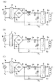
図7及び図8は、チョーク入力型平滑回路を用いたスイッチング電源装置の従来例の構成を示す回路図である。
一般に、スイッチング電源装置はDC−DCコンバータ5のスイッチングによって直流電力を出力するものであるから、DC−DCコンバータ5内の後述するスイッチング制御回路が先ず作動して駆動パルスを出力する必要があり、そのための電源電力をどこから入力するかが問題になる。
【0007】
図7は、チョークコイルCHをダイオードブリッジ3の下流すなわち1次直流電力のホットライン4pに直列に設けた場合の一例を示し、DC−DCコンバータ5内の図示しないスイッチング制御回路の、他端がコモンライン4nに接続された電源入力端子の一端に接続されたソースラインSLが、それぞれチョークコイルCHの下流(コンデンサC1)側のホットライン4pに接続されている。
【0008】
すなわち、ソースラインSLは、図7の(A)ではチョークコイルCHとコンデンサC1の間のホットライン4pに直列に挿入された共振防止用のダイオードD1の下流に、図7の(B)ではチョークコイルCHとダイオードD1との間にそれぞれ接続されて、スイッチング制御回路のための電力が供給されている。
【0009】
図8は、チョークコイルCHをダイオードブリッジ3の上流すなわち交流電源ライン(以下「ACライン」という)のいずれか、例えばACライン1aに直列に設けた場合の一例を示し、ソースラインSLは、図8の(A)ではダイオードブリッジ3の正の出力端子に、図8の(B)ではチョークコイルCHが接続されていないACライン1bに、それぞれ接続されている。
【0010】
【発明が解決しようとする課題】
しかしながら、既に説明したように、低周波用のチョークコイルCHは大きなインダクタンスを必要とし、インダクタンスが大きくなるほどコアのサイズが大きくなると共にコイルの巻数も多くなるため、必然的にコイルの抵抗が大きくなることは避けられない。
【0011】
また、平滑回路のコンデンサC1の端子間電圧Vcを交流電源電圧の実効値を1として表わし、理想的すなわちチョークコイルCHの抵抗分もコンデンサC1の損失もゼロとすれば、図9に示すように、出力電流がゼロの時は電圧Vcが1.41になる。出力電流が増えるに従って、コンデンサ入力型では電圧Vcが次第に低下してゆくが、チョーク入力型では始めに急激に低下し、1に達すると安定化する。インダクタンスが大きいほど初期の低下が著しいが、速やかに安定化する。
【0012】
実際の回路では、チョーク入力型は主としてチョークコイルCHの抵抗分による電圧降下が加わって破線で示したようになり、コンデンサ入力型もコンデンサC1の損失等によって図示した曲線よりも低くなるが、チョーク入力型の方がコンデンサ入力型に比べて、出力電流が大きければ出力電流による電圧Vcの変動が少ないが、出力電流が少ない間は逆に変動が大きくなる傾向は変らない。
【0013】
すなわち、端子間電圧Vcの降下分を出力電流によって微分した値である平滑回路の出力インピーダンス(絶対値)は、チョーク入力型においては出力電流が大きい時には殆んどチョークコイルCHの抵抗値で決定され、出力電流が小さい時はインダクタンスに応じた値が抵抗値に加わってくる。
【0014】
一般に、スイッチング電源装置は交流電源電圧が大きく変動しても応じられるため、スイッチング制御回路に供給される電源電圧の変動が大きい上に、駆動パルスが出力されるまではスイッチングが行なわれず、実効的に平滑回路の負荷がゼロであるから、スイッチング制御回路の電源電圧として、許容入力電圧(交流)の最大値の1.4倍という極めて高い電圧が入力する場合がある。その高い電源電圧でもスイッチング制御回路は破壊されることなく、駆動パルスを出力する必要がある。
【0015】
一方、スイッチングが開始された後は、スイッチング電源装置に接続された負荷に直流電力を供給するために、1次整流平滑回路の出力電流すなわち1次直流電流が増大する。したがって、接続された負荷が大きくなればなるほど、1次直流電流が大きくなるから、チョークコイルCHの抵抗分による電圧降下が無視出来なくなる。
【0016】
図7及び図8に示した従来例では、いずれもDC−DCコンバータ5の図示しないスイッチング制御回路に供給される直流電流はチョークコイルCHを通ったものであるから、交流電源10の電圧が許容入力電圧の最小値であってしかも負荷が最大であるような場合には、スイッチング制御回路の電源電圧が低くなり過ぎて駆動パルスの発振が停止する恐れがある。
【0017】
なお、図8の(B)に示した従来例の場合は、チョークコイルCHを通らない交流電流が入力するように思われ易いが、ACライン1bがACライン1aに対して負の時は、コモンライン4nとACライン1bとが同電位になるから、スイッチング制御回路の電源電圧はゼロで電流が流れず、ACライン1bが正の時はコモンライン4nがチョークコイルCH以降のACライン1aと同電位になるから、電源電圧が正になって電流が流れ、その電流がチョークコイルCHを通って交流電源10に戻ることになる。
【0018】
この発明は上記の点に鑑みてなされたものであり、1次直流電力を平滑するチョーク入力型の平滑回路を備えたスイッチング電源装置において、スイッチング制御回路が負荷の変動に影響されることなく常に安定に駆動パルスを出力出来るようにすることを目的とする。
【0019】
【課題を解決するための手段】
この発明は上記の目的を達成するため、交流電源から入力する交流電力を1次直流電力に変換する全波整流回路と、該全波整流回路の出力端子にそれぞれ接続したホットラインとコモンラインと、該ホットラインとコモンラインとの間に接続した大容量のコンデンサと低周波用のチョークコイルとからなるチョーク入力型の平滑回路と、該平滑回路のコンデンサの両端子間に接続した高周波用のトランスの1次巻線とスイッチング素子との直列回路と、該直列回路のスイッチング素子に駆動パルスを出力するパルス幅変調回路を有するスイッチング制御回路と、該スイッチング制御回路の上記パルス幅変調回路が出力する駆動パルスに応じてスイッチング素子が1次直流電力をスイッチングすることにより、上記トランスの2次巻線に誘起される2次交流電力を2次直流電力へに変換して出力する整流平滑回路とを備えたスイッチング電源装置において、それぞれ次のようにしたものである。
【0020】
すなわち、上記チョークコイルを上記全波整流回路と上記コンデンサとの間の上記ホットラインに直列に接続した場合には、上記スイッチング制御回路の電源入力端子の一端を、上記全波整流回路の入力端子にそれぞれ接続される交流電源ラインのうちのいずれか、又は上記全波整流回路と上記チョークコイルとの間の上記ホットラインに接続し、他端を上記コモンラインに接続する。
【0021】
あるいは、上記チョークコイルを上記全波整流回路の入力端子に接続した交流電源ラインのうちのいずれかに直列に接続してもよく、その場合は、上記スイッチング制御回路の電源入力端子の一端を上記交流電源ラインの上記チョークコイルより上記交流電源側に接続し、他端を上記コモンラインに接続する。
そして、上記いずれの場合も、上記電源入力端子の一端と他端との間に、降圧用の抵抗と逆流防止用のダイオードの直列回路と、定電圧用のツェナダイオードと平滑用のコンデンサの並列回路とを互いに直列に接続し、その接続点から上記パルス幅変調回路へ給電するようにしたものである。
【0022】
【発明の実施の形態】
以下、この発明の実施の形態を図面を参照しながら具体的に説明する。
図1は、この発明の第1の実施形態であるチョークコイルが全波整流回路の下流すなわち1次直流電力側に設けられたチョーク入力型の平滑回路を備えたスイッチング電源装置の構成の各例を示す回路図である。
【0023】
図1の(A)乃至(C)にそれぞれ示したスイッチング電源装置は、いずれも交流電源10から交流電力が入力するノイズフィルタ2と、全波整流回路であるダイオードブリッジ3と、チョークコイルCHと大容量のコンデンサC1とからなるチョーク入力型の平滑回路と、チョークコイルCHとコンデンサC1の間に接続した共振防止用のダイオードD1と、コンデンサC1から平滑された1次直流電力を入力して正負の出力端子6p,6nに接続された負荷11に2次直流電力を出力するDC−DCコンバータ5とにより構成されている。
【0024】
交流電源10から供給される交流電力が入力する交流電源ラインであるACライン1a,1bは、それぞれ双方向のノイズを遮断するノイズフィルタ2を介して、ダイオードブリッジ3の各交流入力端子に接続され、ダイオードブリッジ3の正負の出力端子には、それぞれホットライン4pとコモンライン4nとが接続されている。ホットラインとコモンラインはいずれが正であってもよいが、以下の実施形態においては正のラインをホットライン4p、負のラインをコモンライン4nとしている。
【0025】
コモンライン4nはそのままDC−DCコンバータ5の負の入力端子に、ホットライン4pは順に直列にチョークコイルCHと、ダイオードブリッジ3からの電流がDC−DCコンバータ5に流れる向きのダイオードD1とを介してDC−DCコンバータ5の正の入力端子にそれぞれ接続され、DC−DCコンバータ5の正負の入力端子間にコンデンサC1が接続されている。
【0026】
後述するように、DC−DCコンバータ5内の図示しないスイッチング制御回路の、他端がコモンライン4nに接続された電源入力端子の一端に接続されたソースラインSLの先端が、上記の回路のうちのいずれかに接続されるが、その接続点だけが図1の(A)乃至(C)でそれぞれ異なっている。
【0027】
図2は、図1に示したノイズフィルタ2の構成の一例を示す回路図であり、図2に示したノイズフィルタ2は、ACライン1a,1bの間に、コンデンサC4と中点がフレームグランドに落されたコンデンサC5,C6からなる直列回路とが互いに並列に接続され、その下流にそれぞれACライン1a,1bに直列に接続された互いにコアを共有する高周波用のインダクタL1,L2が設けられている。
【0028】
ACライン1a又は1b上の高周波のノイズは、その対称波形(逆相)成分がコンデンサC4によって打ち消され、残りの同相及び非対称波形成分はそれぞれコンデンサC5又はC6を介してフレームグランドにバイパスされる。一方、インダクタL1,L2はそれぞれ双方向から入力するACライン1a,1b上のノイズを遮断して、他方に伝わらないように作用する。
【0029】
したがって、ノイズフィルタ2は、交流電源10から入力するノイズの進入を防止すると共に、スイッチング電源装置内で発生するノイズを交流電源10及びそれに接続された他の機器にリークさせることもない。
インダクタL1,L2はいずれも高周波用であるからインダクタンスが小さく、したがってその抵抗分も極めて小さいから、インダクタL1,L2に流れる電流による電圧降下は問題にならない。
【0030】
図3は、図1に示したDC−DCコンバータ5の構成の一例を示す回路図であり、図3に示したDC−DCコンバータ5は、1次乃至3次巻線N1,N2,N3を有する高周波用のトランス7と、スイッチング素子であるトランジスタ(FETでもよい)Qと、トランジスタQに駆動パルスを出力してスイッチングさせるスイッチング制御回路(SWC)8と、トランジスタQのスイッチングによって2次巻線N2に誘起される2次交流電力を整流平滑して2次直流電力に変換し、出力端子6p,6nを介して負荷11に出力する整流平滑回路9とにより構成されている。
【0031】
トランス7の1次巻線N1とトランジスタQとの直列回路は、コンデンサC1(図1)からホットライン4p,コモンライン4nを介して供給される平滑された1次直流電力の電流を、スイッチング制御回路8から入力する駆動パルスに応じてトランジスタQがスイッチングするから、1次巻線N1に流れる電流のオン・オフによってトランス7の2次巻線N2及び3次巻線N3にそれぞれ2次及び3次交流電力が誘起される。
【0032】
スイッチング制御回路8は、ソースラインSLを介して供給される電力及び3次巻線N3に誘起される3次交流電力を電源として、出力端子6p,6n間の電圧すなわちスイッチング電源装置の出力電圧を検出して予め設定された基準電圧と比較し、検出された出力電圧が高ければ駆動パルスのオンデューティ比を下げ、低ければオンデューティ比を上げることにより、負荷11の変動に関係なく出力電圧が定電圧を維持するように、フィードバック制御する。
【0033】
図4は、図3に示したスイッチング制御回路8の構成の第1の例を示す回路図であり、図4に示したスイッチング制御回路8は、出力端子6p,6nから入力する出力電圧に応じたオンデューティ比の駆動パルスを出力するPWM(パルス幅変調)回路14と、PWM回路14の電源部をそれぞれ構成する抵抗R1,R2とダイオードD2,D3及び定電圧用のツェナダイオードZD,平滑用のコンデンサC3とからなっている。
【0034】
スイッチング制御回路8の一方の電源入力端子である端子8a,8bの間には、降圧用の抵抗R1と逆流防止用のダイオードD2の直列回路と、定電圧用のツェナダイオードZDと平滑用のコンデンサC3の並列回路とが、互いに直列に接続されており、その接続点からPWM回路へ給電する。電源入力端子の一端である端子8aにはソースラインSLが、他端である端子8bにはコモンライン4nが、それぞれ接続されている。
【0035】
スイッチング制御回路8の他方の電源入力端子は、トランス7の3次巻線N3の両端に接続され、トランジスタQのスイッチングによって3次巻線N3に誘起される3次交流電力は、整流用のダイオードD3により整流され、電流制限用の抵抗R2を介してコンデンサC3を充電する。
【0036】
スイッチング電源装置の電源オンの直後は、コンデンサC1(図1)の充電が始まってもコンデンサC3の電圧はゼロであり、PWM回路14が作動しないからスイッチングが行なわれず、3次巻線N3の起電力はゼロのままである。したがって、PWM回路14が駆動パルスを出力し始めるための電源は、専らコモンライン4nに対して正のソースラインSLから供給される(PWM回路14が必要とする電圧より遥かに高い電圧の)直流電力によっている。
【0037】
ソースラインSLを介して端子8aに入力する高い電圧の直流電力は、抵抗R1によって電圧降下され、ツェナダイオードZDによって定電圧化されてコンデンサC3を充電する。コンデンサC3の端子間電圧が或る電圧以上になると、PWM回路14が駆動パルスを出力し始め、トランジスタQがスイッチングを開始するから、コンデンサC3の充電は3次巻線N3からダイオードD3を介して入力する電流がメインになる。
【0038】
しかしながら、スイッチング開始直後は出力端子6p,6nの電圧がゼロであるから、駆動パルスのオンデューティ比は最大になっている。したがって、3次巻線N3に誘起される3次交流電力をダイオードD3で整流したままでコンデンサC3とツェナダイオードZDとの並列回路に供給すると、ツェナダイオードZDに過大な電流が流れて焼損する恐れがある。そのため、電流制限用の抵抗R2を設け、過大な電流が流れないようにしてツェナダイオードZDの焼損を防止している。
【0039】
スイッチング制御回路の構成の第2の例は、特には図示しないが、3次巻線N3を備えてないトランスが用いられた場合の例であって、図4に示したスイッチング制御回路8において、3次巻線N3と共に、スイッチング制御回路8内のダイオードD3と抵抗R2との直列回路を省いたものであるから、詳しい説明は省略する。このスイッチング制御回路の場合は、トランジスタQのスイッチング開始後も、PWM回路14の電源は常にソースラインSLを介して供給される電力のみである。
【0040】
したがって、このようなスイッチング制御回路は、スイッチング開始後のPWM回路14の電源が一部はソースラインSLを介して供給され続けるが、主として3次巻線N3から供給されるスイッチング制御回路8に比べて、構成が簡単でトランスを含めたコストが安いから、特に廉価なスイッチング電源装置に採用されることが多いが、ソースラインSLの電圧変動の影響を受け易いという問題がある。
【0041】
図6は、交流電源10の電圧とソースラインSLの電圧の一例を示す波形図であり、交流電源電圧はACライン1bを基準としたACライン1aの電圧で表わし、ソースラインSLの電圧はコモンライン4nを基準として、A,B,C3種類の電圧波形を示している。
図6に示したソースライン電圧A,B,Cの各波形は、説明を容易にするため、交流電源電圧に対して、チョークコイルCHによる位相ズレがないものとして示している。
【0042】
図1の(A),(B)又は(C)は、第1の実施形態におけるそれぞれソースラインSLをACライン1a,1b又はダイオードブリッジ3の正の出力端子に接続した場合の例を示し、ソースライン電圧はそれぞれ図6のB,C又はAに示した波形になる。
【0043】
すなわち、ソースラインSLを、図1の(A)に示したようにACライン1a(ノイズフィルタ2以前でも同じ)に接続すると、ソースライン電圧は図6のBに示したように、交流電源電圧が正の間はコモンライン4nとACライン1bとが同電位になるから、ソースライン電圧はACライン1aと共に正になって電流が流れる。逆に、交流電源電圧が負の間はコモンライン4nとACライン1aとが同電位になるから、ソースライン電圧はゼロになって電流が流れない。
【0044】
ソースラインSLを、図1の(B)に示したようにACライン1b(ノイズフィルタ2以前でも同じ)に接続すると、ソースライン電圧は図6のCに示したように、交流電源電圧が正の間はコモンライン4nとACライン1bとが同電位になるから、ソースライン電圧はゼロになって電流が流れない。逆に、交流電源電圧が負の間はコモンライン4nとACライン1aとが同電位になるから、ソースライン電圧はACライン1bと共に正になって電流が流れる。
【0045】
ソースラインSLを、図1の(C)に示したようにダイオードブリッジ3の正の出力端子、すなわちダイオードブリッジ3とチョークコイルCHとの間のホットライン4pに接続すると、該ホットライン4pの電圧はコモンライン4nに対して正弦波形の絶対値すなわち全波整流波形を示すから、ソースライン電圧は図6のAに示した波形になる。
【0046】
図1に示した各実施形態のうち特に図1の(C)に示した実施形態が、図7の(A),(B)に示した従来例と異なるところは、ソースラインSLのホットライン4pに対する接続点がチョークコイルCHの前にあるか後にあるかという点である。DC−DCコンバータ5のスイッチング開始以前は負荷11の影響がゼロであるから、両者の差は殆んどない。
【0047】
しかしながら、DC−DCコンバータ5のスイッチングが開始されると、負荷11の変動によってチョークコイルCHに流れる電流が大きく変化するから、図7に示した従来例においてはソースラインSLの電圧が交流電源電圧の変動に加えて負荷11の変動に大きく影響されるが、図1に示した実施形態では全く影響されることがなく、交流電源電圧の変動のみになる。
【0048】
したがって、ソースラインSLからの電源のみに依存するスイッチング制御回路の第2の例では、そのちがいが極めて大きく、従来例では駆動パルスの発振停止の恐れが生じるような場合でも、この実施形態においては負荷の変動による発振停止は発生しない。
【0049】
また、第1の例の3次巻線N3からも電力供給を受けるスイッチング制御回路8であっても、第2の例と同様にソースライン電圧の変動が少なければ、電圧降下用の抵抗R1の抵抗値の決定が容易で、電力容量の少ないツェナダイオードZDを選択することが出来るから、抵抗R1の電圧降下による電力ロスを小さくすることが出来る。
【0050】
図5は、この発明の第2の実施形態であるチョークコイルが全波整流回路の上流すなわち交流電源10側に設けられたチョーク入力型の平滑回路を備えたスイッチング電源装置の構成の各例を示す回路図であり、図1に示した第1の実施形態と同一部分には同一符号を付して説明を省略する。
【0051】
図5に示したスイッチング電源装置が、図1に示したスイッチング電源装置と異なるところは、ダイオードブリッジ3の出力側にあったチョークコイルCHをその入力側に移すと共に、不要になった共振防止用のダイオードD1を廃止したことである。チョークコイルCHは、ACライン1a,1bのいずれに設けてもよいが、図5に示したスイッチング電源装置では、ノイズフィルタ2とダイオードブリッジ3との間のACライン1aに直列に設けている。
【0052】
図5に示したスイッチング電源装置は、DC−DCコンバータ5の(スイッチング制御回路8の)ソースラインSLが、チョークコイルCHを設けたACライン1aのチョークコイルCHより交流電源10側に接続され、図5の(A)はノイズフィルタ2とダイオードブリッジ3との間に、図5の(B)はノイズフィルタ2より交流電源10側にそれぞれ接続した例を示している。
【0053】
図2に示したノイズフィルタ2の説明で述べたように、ノイズフィルタ2のインダクタL1又はL2による電圧降下は、インダクタL1,L2の抵抗値がチョークコイルCHの抵抗値に比べて遙かに小さく、問題にならないから、図5の(A)と(B)に示した例は、実際的に同じものと考えてもよい。
【0054】
図5に示した第2の実施形態であるスイッチング電源装置を、図8に示した従来例と比較すると、図8の(B)に示した従来例とのちがいは、ソースラインSLの接続先がACライン1aであるか、ACライン1bであるかのちがいであり、その結果としてソースライン電圧は、図5の(A),(B)に示した実施形態では図6のBに示した波形を示し、図8の(B)に示した従来例では図6のCに示した波形を示す。
【0055】
図8の(A)に示した従来例は、図5の(A),(B)に示した実施形態及び図8の(B)に示した従来例と異なり、ソースラインSLの接続先がACライン1a,1bではなく、ダイオードブリッジ3の正の出力端子又はホットライン4pであって、ソースライン電圧は図6のAに示した波形になっている。
【0056】
図5の(A),(B)に示した実施形態は、図6のBに示したように、交流電源電圧が正の間だけチョークコイルCHを通らずにACライン1aから直接にソースラインSLを介して電流が流れるのに対して、図8の(B)に示した従来例は、図6のCに示したように、交流電源電圧が負の間だけACライン1bからソースラインSLを介して電流が流れる。
【0057】
したがって、スイッチング制御回路に流れた電流は、コモンライン4nからACライン1aとチョークコイルCHを通って交流電源10に戻る。
図8の(A)に示した従来例も、交流電源電圧が正であっても負であっても、ソースラインSLに流れる電流は必ずチョークコイルCHを通って交流電源10に戻る。
【0058】
すなわち、従来例のソースライン電圧がチョークコイルCHによる電圧降下の影響を受けるのに対して、第2の実施形態ではソースライン電圧がチョークコイルCHによる電圧降下すなわち負荷の変動の影響を受けないことは、第1の実施形態と同様であり、したがってその効果も第1の実施形態と同じである。
【0059】
このように、スイッチング制御回路8の電源電圧の変動が、交流電源10の電圧変動の影響のみで負荷変動の影響を受けなければ、それだけ変動幅が少なくなるため、その変動を吸収するツェナダイオードZDの負担が少なくなるのみならず、ツェナダイオードZDと電圧降下用の抵抗R1の発熱すなわち電力損失を予め小さく設定することが出来るから、省エネルギの効果も得られる。
【0060】
なお、参考ながら、図1の(C)に示した実施形態は、ソースラインSLをダイオードブリッジ3とチョークコイルCHとの間に接続した点で、例えば特開平6−98542号公報の図1に示された回路に、また図5の(B)に示した実施形態は、ソースラインSLをノイズフィルタ2の前段ACライン1aに接続した点で、例えば特開平6−78542号公報の図1に示された回路に、それぞれ類似しているように見える。
【0061】
しかしながら、前者の特開平6−98542号公報の図1に示された回路は、昇圧型コンバータ回路であるから、チョークコイルL1はスイッチング周波数に対応する高周波用のものであり、インダクタンスも抵抗値も小さいから電圧降下が問題になるものではない。さらに、PWM制御回路5からのラインは、整流器RC1の出力端電圧を検出するためのものであって、電源ラインとして電力を入力するものではない。したがって、図1の(C)に示した実施形態とは全く異なるものである。
【0062】
また、後者の特開平6−78542号公報の図1に示された回路は、力率を改善するための回路であり、コンデンサ入力型の平滑回路であるからチョークコイルは存在しない。したがって、制御回路10の電源ラインを交流入力電源1からのACラインのいずれに接続しても変らないから、図5の(B)に示した実施形態とは全く異なるものである。
【0063】
【発明の効果】
以上説明したように、この発明による1次直流電力を平滑するチョーク入力型の平滑回路を備えたスイッチング電源装置は、スイッチング制御回路が負荷の変動に影響されることなく駆動パルスを出力するから、常に安定したスイッチングを行なうことができる。
【図面の簡単な説明】
【図1】この発明の第1の実施形態であるチョークコイルを全波整流回路の下流に設けたスイッチング電源装置の構成の例を示す回路図である。
【図2】図1に示したノイズフィルタの構成の一例を示す回路図である。
【図3】図1に示したDC−DCコンバータの構成の一例を示す回路図である。
【図4】図3に示したスイッチング制御回路の構成の一例を示す回路図である。
【図5】この発明の第2の実施形態であるチョークコイルを全波整流回路の上流に設けたスイッチング電源装置の構成の例を示す回路図である。
【図6】交流電源電圧と各実施形態ならびに従来例におけるソースライン電圧の例とを示す波形図である。
【図7】チョークコイルを全波整流回路の下流に設けたスイッチング電源装置の従来例の構成を示す回路図である。
【図8】チョークコイルを全波整流回路の上流に設けたスイッチング電源装置の従来例の構成を示す回路図である。
【図9】チョーク入力型及びコンデンサ入力型の平滑回路の出力電流に対するコンデンサの端子間電圧の変化の一例を示す線図である。
【符号の説明】
1a,1b:ACライン(交流電源ライン)
2:ノイズフィルタ
3:ダイオードブリッジ(全波整流回路)
4p:ホットライン 4n:コモンライン
5:DC−DCコンバータ 7:トランス
8:スイッチング制御回路
8a,8b:(スイッチング制御回路の)電源入力端子
9:整流平滑回路 10:交流電源
11:負荷 14:PWM回路
C1,C3:コンデンサ CH:チョークコイル
N1〜N3:(トランスの)1次巻線〜3次巻線
Q:トランジスタ(スイッチング素子)
SL:ソースライン ZD:ツェナダイオード[0001]
BACKGROUND OF THE INVENTION
The present invention relates to a switching power supply device that performs switching in accordance with a drive pulse output from a switching control circuit, and more particularly, to a power supply input terminal of a switching control circuit that must start operation in the switching power supply device after the power is turned on. Regarding connection.
[0002]
[Prior art]
AC power input from an AC power source (hereinafter referred to as “primary AC power”) is rectified and smoothed to be converted into primary DC power, and the primary DC power is converted into secondary DC power of an arbitrary voltage by a DC-DC converter. A switching power supply device that converts and outputs the load to a load is small, light, low in cost, and excellent in power conversion efficiency. Furthermore, even if the voltage and frequency of the primary AC power change significantly, a constant voltage of DC power can always be obtained. Therefore, it is widely used as a power supply device for various electronic devices.
[0003]
When primary AC power is converted to primary DC power, the rectifier circuit is almost a full-wave rectifier type using a diode bridge, and a capacitor input type and a choke input type are widely known as smoothing circuits.
Capacitor input type smoothing circuit is simple in configuration and low in cost, but the conduction angle of AC current is narrow and its peak value is large, resulting in poor power factor. Therefore, the generated electric noise is large and adversely affects the AC power supply and other devices connected thereto.
[0004]
On the other hand, the choke input type smoothing circuit has a wide conduction angle, which suppresses the current peak value and noise and improves the power factor. However, in order to obtain the result even at a low frequency such as a commercial power supply frequency, several Since inductance of mH to several tens of mH is required, there is a problem that the choke coil becomes large and heavy, and the size and cost of the entire power supply device cannot be avoided.
[0005]
However, as the number of devices connected to the same power supply increases with the types of electronic devices recently, the negative effects on other devices such as noise and power supply voltage drop cannot be ignored, and power factor improvement and noise suppression are severe. Therefore, a noise filter is provided in the power input section, an active filter is provided in front of the capacitor input type smoothing circuit as a primary DC power smoothing circuit, or the power factor is improved in place of the choke input type smoothing circuit. The number is increasing.
[0006]
7 and 8 are circuit diagrams showing a configuration of a conventional example of a switching power supply device using a choke input type smoothing circuit.
In general, since the switching power supply device outputs DC power by switching of the DC-
[0007]
FIG. 7 shows an example in which the choke coil CH is provided downstream of the
[0008]
That is, the source line SL is downstream of the resonance preventing diode D1 inserted in series in the
[0009]
FIG. 8 shows an example in which the choke coil CH is provided upstream of the
[0010]
[Problems to be solved by the invention]
However, as already described, the low-frequency choke coil CH requires a large inductance, and the larger the inductance, the larger the core size and the number of turns of the coil, which inevitably increases the resistance of the coil. It is inevitable.
[0011]
Further, when the effective value of the AC power supply voltage is expressed as 1 with respect to the voltage Vc between the terminals of the capacitor C1 of the smoothing circuit, and ideally, that is, the resistance of the choke coil CH and the loss of the capacitor C1 are zero, as shown in FIG. When the output current is zero, the voltage Vc is 1.41. As the output current increases, in the capacitor input type, the voltage Vc gradually decreases, but in the choke input type, the voltage suddenly decreases first, and when it reaches 1, it stabilizes. The larger the inductance is, the more the initial decrease is, but it is stabilized quickly.
[0012]
In an actual circuit, the choke input type has a voltage drop mainly due to the resistance of the choke coil CH and is shown by a broken line, and the capacitor input type is also lower than the curve shown by the loss of the capacitor C1, etc. The input type has less fluctuation of the voltage Vc due to the output current if the output current is larger than the capacitor input type, but the tendency that the fluctuation becomes larger does not change while the output current is small.
[0013]
That is, the output impedance (absolute value) of the smoothing circuit, which is a value obtained by differentiating the drop in the inter-terminal voltage Vc by the output current, is almost determined by the resistance value of the choke coil CH when the output current is large in the choke input type. When the output current is small, a value corresponding to the inductance is added to the resistance value.
[0014]
In general, a switching power supply can respond even if the AC power supply voltage fluctuates greatly. Therefore, the power supply voltage supplied to the switching control circuit is largely fluctuated, and switching is not performed until a drive pulse is output. In addition, since the load of the smoothing circuit is zero, a very high voltage of 1.4 times the maximum value of the allowable input voltage (AC) may be input as the power supply voltage of the switching control circuit. It is necessary to output a drive pulse without destroying the switching control circuit even at the high power supply voltage.
[0015]
On the other hand, after switching is started, the output current of the primary rectifying / smoothing circuit, that is, the primary DC current increases in order to supply DC power to the load connected to the switching power supply device. Therefore, as the connected load increases, the primary DC current increases, so that the voltage drop due to the resistance of the choke coil CH cannot be ignored.
[0016]
In the conventional examples shown in FIGS. 7 and 8, since the direct current supplied to the switching control circuit (not shown) of the DC-
[0017]
In the case of the conventional example shown in FIG. 8B, an alternating current that does not pass through the choke coil CH is likely to be input, but when the
[0018]
The present invention has been made in view of the above points. In a switching power supply apparatus including a choke input type smoothing circuit that smoothes primary DC power, the switching control circuit is always affected by fluctuations in the load. The purpose is to be able to output drive pulses stably.
[0019]
[Means for Solving the Problems]
In order to achieve the above object, the present invention provides a full-wave rectifier circuit that converts AC power input from an AC power source into primary DC power, and a hot line and a common line that are respectively connected to output terminals of the full-wave rectifier circuit. , A choke input type smoothing circuit comprising a large-capacitance capacitor connected between the hot line and the common line and a choke coil for low frequency, and a high frequency circuit connected between both terminals of the capacitor of the smoothing circuit. A series circuit of a primary winding of a transformer and a switching element, and a drive pulse is output to the switching element of the series circuitHas pulse width modulation circuitSwitching control circuit and the switching control circuit described abovePulse width modulation circuitThe switching element switches the primary DC power according to the drive pulse output bythe aboveIn the switching power supply device including the rectifying and smoothing circuit that converts the secondary AC power induced in the secondary winding of the transformer into the secondary DC power and outputs the converted power, the following is performed.
[0020]
That is,the abovechoke coilThe aboveFull-wave rectifier circuit andthe aboveBetween the capacitorthe aboveConnected in series to the hotlinein case of,the aboveOne end of the power input terminal of the switching control circuitthe aboveOne of the AC power lines connected to the input terminals of the full-wave rectifier circuit, orthe aboveFull-wave rectifier circuit andthe aboveBetween the choke coilthe aboveConnect to the hotline and connect the other endthe aboveConnect to common lineDo.
[0021]
Orthe abovechoke coilThe aboveConnected in series to one of the AC power lines connected to the input terminal of the full-wave rectifier circuitMay,In that case, the aboveOne end of the power input terminal of the switching control circuit from the choke coil of the AC power supply lineAC power supply sideConnect the other endthe aboveConnect to common lineDo.
And in any of the above cases,UpA series circuit of a step-down resistor and a backflow prevention diode and a parallel circuit of a constant voltage zener diode and a smoothing capacitor are connected in series between one end and the other end of the power input terminal. The power is fed from the connection point to the pulse width modulation circuit.
[0022]
DETAILED DESCRIPTION OF THE INVENTION
Embodiments of the present invention will be specifically described below with reference to the drawings.
FIG. 1 shows each example of the configuration of a switching power supply apparatus including a choke input type smoothing circuit in which the choke coil according to the first embodiment of the present invention is provided downstream of the full-wave rectifier circuit, that is, on the primary DC power side. FIG.
[0023]
Each of the switching power supply devices shown in FIGS. 1A to 1C includes a
[0024]
[0025]
The common line 4n is directly connected to the negative input terminal of the DC-
[0026]
As will be described later, the tip of the source line SL connected to one end of the power input terminal whose other end is connected to the common line 4n of the switching control circuit (not shown) in the DC-
[0027]
FIG. 2 is a circuit diagram showing an example of the configuration of the
[0028]
The high-frequency noise on the
[0029]
Therefore, the
Since both the inductors L1 and L2 are for high frequency use, the inductance is small, and therefore the resistance is very small. Therefore, the voltage drop due to the current flowing through the inductors L1 and L2 is not a problem.
[0030]
FIG. 3 is a circuit diagram showing an example of the configuration of the DC-
[0031]
The series circuit of the primary winding N1 of the transformer 7 and the transistor Q switches the current of the smoothed primary DC power supplied from the capacitor C1 (FIG. 1) via the
[0032]
The switching
[0033]
FIG. 4 is a circuit diagram showing a first example of the configuration of the switching
[0034]
Between one power
[0035]
The other power input terminal of the switching
[0036]
Immediately after the switching power supply is turned on, even if charging of the capacitor C1 (FIG. 1) starts, the voltage of the capacitor C3 is zero and the
[0037]
The high-voltage DC power input to the terminal 8a via the source line SL is dropped by the resistor R1, and is made constant by the Zener diode ZD to charge the capacitor C3. When the voltage between the terminals of the capacitor C3 exceeds a certain voltage, the
[0038]
However, since the voltage at the
[0039]
A second example of the configuration of the switching control circuit is an example in the case where a transformer not provided with the tertiary winding N3 is used, although not particularly illustrated. In the
[0040]
Therefore, in such a switching control circuit, a part of the power supply of the
[0041]
FIG. 6 is a waveform diagram showing an example of the voltage of the
Each waveform of the source line voltages A, B, and C shown in FIG. 6 is shown as having no phase shift due to the choke coil CH with respect to the AC power supply voltage for easy explanation.
[0042]
(A), (B), or (C) of FIG. 1 shows an example in which the source line SL in the first embodiment is connected to the
[0043]
That is, when the source line SL is connected to the
[0044]
When the source line SL is connected to the
[0045]
When the source line SL is connected to the positive output terminal of the
[0046]
Among the embodiments shown in FIG. 1, the embodiment shown in FIG. 1C differs from the conventional example shown in FIGS. 7A and 7B in that the hot line of the source line SL is different. The connection point for 4p is in front of or behind the choke coil CH. Since the influence of the
[0047]
However, when the switching of the DC-
[0048]
Therefore, in the second example of the switching control circuit that depends only on the power source from the source line SL, the difference is extremely large, and even in the case where there is a risk of stopping the oscillation of the drive pulse in the conventional example, in this embodiment, Oscillation stop due to load fluctuation does not occur.
[0049]
Further, even in the switching
[0050]
FIG. 5 shows each example of the configuration of a switching power supply apparatus including a choke input type smoothing circuit in which the choke coil according to the second embodiment of the present invention is provided upstream of the full-wave rectifier circuit, that is, on the
[0051]
The switching power supply device shown in FIG. 5 differs from the switching power supply device shown in FIG. 1 in that the choke coil CH on the output side of the
[0052]
In the switching power supply shown in FIG. 5, the source line SL (of the switching control circuit 8) of the DC-
[0053]
As described in the description of the
[0054]
When the switching power supply according to the second embodiment shown in FIG. 5 is compared with the conventional example shown in FIG. 8, the connection destination of the source line SL is different from the conventional example shown in FIG. Is the
[0055]
8A is different from the embodiment shown in FIGS. 5A and 5B and the conventional example shown in FIG. 8B in that the connection destination of the source line SL is different. It is not the
[0056]
In the embodiment shown in FIGS. 5A and 5B, as shown in FIG. 6B, the source line is directly connected from the
[0057]
Therefore, the current flowing through the switching control circuit returns from the common line 4n to the
In the conventional example shown in FIG. 8A as well, regardless of whether the AC power supply voltage is positive or negative, the current flowing through the source line SL always returns to the
[0058]
That is, the source line voltage in the conventional example is affected by the voltage drop caused by the choke coil CH, whereas in the second embodiment, the source line voltage is not affected by the voltage drop caused by the choke coil CH, that is, the load fluctuation. Is the same as that of the first embodiment, and therefore the effect is the same as that of the first embodiment.
[0059]
In this way, if the fluctuation of the power supply voltage of the switching
[0060]
For reference, in the embodiment shown in FIG. 1C, the source line SL is connected between the
[0061]
However, since the circuit shown in FIG. 1 of the former JP-A-6-98542 is a step-up converter circuit, the choke coil L1 is for a high frequency corresponding to the switching frequency, and has both an inductance and a resistance value. The voltage drop is not a problem because it is small. Furthermore, the line from the
[0062]
Further, the circuit shown in FIG. 1 of the latter Japanese Patent Laid-Open No. 6-78542 is a circuit for improving the power factor and is a capacitor input type smoothing circuit, so there is no choke coil. Therefore, since the power supply line of the
[0063]
【The invention's effect】
As described above, the switching power supply device including the choke input type smoothing circuit for smoothing the primary DC power according to the present invention outputs the drive pulse without being affected by the load fluctuation. Stable switching can always be performed.
[Brief description of the drawings]
FIG. 1 is a circuit diagram showing an example of the configuration of a switching power supply device in which a choke coil according to a first embodiment of the present invention is provided downstream of a full-wave rectifier circuit.
2 is a circuit diagram illustrating an example of a configuration of a noise filter illustrated in FIG. 1;
3 is a circuit diagram showing an example of the configuration of the DC-DC converter shown in FIG. 1. FIG.
4 is a circuit diagram showing an example of a configuration of a switching control circuit shown in FIG. 3;
FIG. 5 is a circuit diagram showing an example of the configuration of a switching power supply device in which a choke coil according to a second embodiment of the present invention is provided upstream of a full-wave rectifier circuit.
FIG. 6 is a waveform diagram showing an AC power supply voltage and an example of a source line voltage in each embodiment and a conventional example.
FIG. 7 is a circuit diagram showing a configuration of a conventional example of a switching power supply device in which a choke coil is provided downstream of a full-wave rectifier circuit.
FIG. 8 is a circuit diagram showing a configuration of a conventional example of a switching power supply device in which a choke coil is provided upstream of a full-wave rectifier circuit.
FIG. 9 is a diagram showing an example of a change in voltage between terminals of a capacitor with respect to an output current of a smoothing circuit of a choke input type and a capacitor input type.
[Explanation of symbols]
1a, 1b: AC line (AC power supply line)
2: Noise filter
3: Diode bridge (full-wave rectifier circuit)
4p: Hot line 4n: Common line
5: DC-DC converter 7: Transformer
8: Switching control circuit
8a, 8b: Power supply input terminals (of the switching control circuit)
9: Rectification smoothing circuit 10: AC power supply
11: Load 14: PWM circuit
C1, C3: Capacitor CH: Choke coil
N1-N3: Primary winding to tertiary winding (of transformer)
Q: Transistor (switching element)
SL: Source line ZD: Zener diode
Claims (2)
前記ホットラインに直列に接続した低周波用のチョークコイルと該チョークコイルの出力側の前記ホットラインと前記コモンラインとの間に接続した大容量のコンデンサとからなるチョーク入力型の平滑回路と、
該平滑回路のコンデンサの両端子間に接続した高周波用のトランスの1次巻線とスイッチング素子との直列回路と、
該直列回路のスイッチング素子に駆動パルスを出力するパルス幅変調回路を有するスイッチング制御回路と、
該スイッチング制御回路の前記パルス幅変調回路が出力する駆動パルスに応じて前記スイッチング素子が前記1次直流電力をスイッチングすることにより、前記トランスの2次巻線に誘起される2次交流電力を2次直流電力に変換して出力する整流平滑回路とを備えたスイッチング電源装置において、
前記スイッチング制御回路の電源入力端子の一端を、前記全波整流回路の入力端子にそれぞれ接続される交流電源ラインのうちのいずれか、又は前記全波整流回路と前記チョークコイルとの間のホットラインに接続し、他端を前記コモンラインに接続するとともに、
前記電源入力端子の一端と他端との間に、降圧用の抵抗と逆流防止用のダイオードの直列回路と、定電圧用のツェナダイオードと平滑用のコンデンサの並列回路とを互いに直列に接続し、その接続点から前記パルス幅変調回路へ給電するようにしたことを特徴とするスイッチング電源装置。A full-wave rectifier circuit that converts AC power input from an AC power source into primary DC power; a hot line and a common line connected to the output terminals of the full-wave rectifier circuit;
A smoothing circuit of a choke input type consisting of a large-capacity capacitor connected between an output side of the hot line and the common line of the choke coil and the choke coil for low frequency connected in series with the hot line,
A series circuit of a primary winding of a high-frequency transformer and a switching element connected between both terminals of the capacitor of the smoothing circuit;
A switching control circuit having a pulse width modulation circuit that outputs a driving pulse to the switching element of the series circuit;
The switching element switches the primary DC power according to the drive pulse output from the pulse width modulation circuit of the switching control circuit , so that the secondary AC power induced in the secondary winding of the transformer is 2 In a switching power supply device comprising a rectifying and smoothing circuit that converts and outputs secondary DC power,
One end of the power input terminal of the switching control circuit is one of the AC power lines connected to the input terminal of the full wave rectifier circuit, or a hot line between the full wave rectifier circuit and the choke coil And the other end to the common line ,
A series circuit of a step-down resistor and a backflow prevention diode and a parallel circuit of a constant voltage zener diode and a smoothing capacitor are connected in series between one end and the other end of the power input terminal. A switching power supply device wherein power is supplied from the connection point to the pulse width modulation circuit .
前記全波整流回路の入力端子に接続した交流電源ラインのうちのいずれかに直列に接続した低周波用のチョークコイルと前記ホットラインとコモンラインとの間に接続した大容量のコンデンサとからなるチョーク入力型の平滑回路と、
該平滑回路のコンデンサの両端子間に接続した高周波用のトランスの1次巻線とスイッチング素子との直列回路と、
該直列回路のスイッチング素子に駆動パルスを出力するパルス幅変調回路を有するスイッチング制御回路と、
該スイッチング制御回路の前記パルス幅変調回路が出力する駆動パルスに応じて前記スイッチング素子が前記1次直流電力をスイッチングすることにより、前記トランスの2次巻線に誘起される2次交流電力を2次直流電力に変換して出力する整流平滑回路とを備えたスイッチング電源装置において、
前記スイッチング制御回路の電源入力端子の一端を、前記交流電源ラインの前記チョークコイルより前記交流電源側に接続し、他端を前記コモンラインに接続するとともに、
前記電源入力端子の一端と他端との間に、降圧用の抵抗と逆流防止用のダイオードの直列回路と、定電圧用のツェナダイオードと平滑用のコンデンサの並列回路とを互いに直列に接続し、その接続点から前記パルス幅変調回路へ給電するようにしたことを特徴とするスイッチング電源装置。A full-wave rectifier circuit that converts AC power input from an AC power source into primary DC power; a hot line and a common line connected to the output terminals of the full-wave rectifier circuit;
A low-frequency choke coil connected in series to one of the AC power supply lines connected to the input terminal of the full-wave rectifier circuit, and a large-capacitance capacitor connected between the hot line and the common line. A choke input type smoothing circuit;
A series circuit of a primary winding of a high-frequency transformer and a switching element connected between both terminals of the capacitor of the smoothing circuit;
A switching control circuit having a pulse width modulation circuit that outputs a driving pulse to the switching element of the series circuit;
The switching element switches the primary DC power according to the drive pulse output from the pulse width modulation circuit of the switching control circuit , so that the secondary AC power induced in the secondary winding of the transformer is 2 In a switching power supply device comprising a rectifying and smoothing circuit that converts and outputs secondary DC power,
One end of the power input terminal of the switching control circuit is connected to the AC power supply side from the choke coil of the AC power supply line, and the other end is connected to the common line ,
A series circuit of a step-down resistor and a backflow prevention diode and a parallel circuit of a constant voltage zener diode and a smoothing capacitor are connected in series between one end and the other end of the power input terminal. A switching power supply device wherein power is supplied from the connection point to the pulse width modulation circuit .
Priority Applications (1)
| Application Number | Priority Date | Filing Date | Title |
|---|---|---|---|
| JP05178196A JP3676873B2 (en) | 1996-03-08 | 1996-03-08 | Switching power supply |
Applications Claiming Priority (1)
| Application Number | Priority Date | Filing Date | Title |
|---|---|---|---|
| JP05178196A JP3676873B2 (en) | 1996-03-08 | 1996-03-08 | Switching power supply |
Publications (2)
| Publication Number | Publication Date |
|---|---|
| JPH09247941A JPH09247941A (en) | 1997-09-19 |
| JP3676873B2 true JP3676873B2 (en) | 2005-07-27 |
Family
ID=12896499
Family Applications (1)
| Application Number | Title | Priority Date | Filing Date |
|---|---|---|---|
| JP05178196A Expired - Fee Related JP3676873B2 (en) | 1996-03-08 | 1996-03-08 | Switching power supply |
Country Status (1)
| Country | Link |
|---|---|
| JP (1) | JP3676873B2 (en) |
Cited By (1)
| Publication number | Priority date | Publication date | Assignee | Title |
|---|---|---|---|---|
| WO2009153173A1 (en) * | 2008-06-20 | 2009-12-23 | Continental Automotive Gmbh | Filter device |
Families Citing this family (1)
| Publication number | Priority date | Publication date | Assignee | Title |
|---|---|---|---|---|
| JP5565149B2 (en) * | 2010-07-01 | 2014-08-06 | 富士電機株式会社 | Power converter |
-
1996
- 1996-03-08 JP JP05178196A patent/JP3676873B2/en not_active Expired - Fee Related
Cited By (3)
| Publication number | Priority date | Publication date | Assignee | Title |
|---|---|---|---|---|
| WO2009153173A1 (en) * | 2008-06-20 | 2009-12-23 | Continental Automotive Gmbh | Filter device |
| US8878456B2 (en) | 2008-06-20 | 2014-11-04 | Continental Automotive Gmbh | Filter device |
| DE102008029478B4 (en) * | 2008-06-20 | 2015-10-08 | Continental Automotive Gmbh | control module |
Also Published As
| Publication number | Publication date |
|---|---|
| JPH09247941A (en) | 1997-09-19 |
Similar Documents
| Publication | Publication Date | Title |
|---|---|---|
| US6483731B1 (en) | Alexander topology resonance energy conversion and inversion circuit utilizing a series capacitance multi-voltage resonance section | |
| JP3260024B2 (en) | Power circuit | |
| JP2001112253A (en) | DC-to-DC CONVERTER | |
| JPH06209574A (en) | Power supply circuit | |
| EP1102387A2 (en) | DC power supply apparatus | |
| JP3151932B2 (en) | Power supply circuit | |
| JP3676873B2 (en) | Switching power supply | |
| JP4143154B2 (en) | Power supply device and electronic device | |
| JP3587907B2 (en) | DC power supply | |
| JP2001103762A (en) | Power factor improving circuit | |
| JP3346443B2 (en) | Switching power supply | |
| JP3400132B2 (en) | Switching power supply | |
| JP3571959B2 (en) | Switching power supply | |
| JP3590152B2 (en) | DC power supply | |
| JP3235295B2 (en) | Power supply | |
| JP3277551B2 (en) | Power circuit | |
| JP3461072B2 (en) | Switching power supply | |
| JPH09131055A (en) | Switching regulator | |
| JPH11164552A (en) | Power supply | |
| JP4443651B2 (en) | Power supply | |
| JPH0591733A (en) | Power supply device | |
| JP2790326B2 (en) | Switching regulator | |
| JPH10127048A (en) | Power conversion device | |
| JP3453468B2 (en) | Switching regulator | |
| JP2000232789A (en) | Power supply device |
Legal Events
| Date | Code | Title | Description |
|---|---|---|---|
| A977 | Report on retrieval |
Free format text: JAPANESE INTERMEDIATE CODE: A971007 Effective date: 20050125 |
|
| A131 | Notification of reasons for refusal |
Free format text: JAPANESE INTERMEDIATE CODE: A131 Effective date: 20050201 |
|
| A521 | Written amendment |
Free format text: JAPANESE INTERMEDIATE CODE: A523 Effective date: 20050404 |
|
| TRDD | Decision of grant or rejection written | ||
| A01 | Written decision to grant a patent or to grant a registration (utility model) |
Free format text: JAPANESE INTERMEDIATE CODE: A01 Effective date: 20050426 |
|
| A61 | First payment of annual fees (during grant procedure) |
Free format text: JAPANESE INTERMEDIATE CODE: A61 Effective date: 20050502 |
|
| R150 | Certificate of patent or registration of utility model |
Free format text: JAPANESE INTERMEDIATE CODE: R150 |
|
| FPAY | Renewal fee payment (event date is renewal date of database) |
Free format text: PAYMENT UNTIL: 20110513 Year of fee payment: 6 |
|
| FPAY | Renewal fee payment (event date is renewal date of database) |
Free format text: PAYMENT UNTIL: 20110513 Year of fee payment: 6 |
|
| FPAY | Renewal fee payment (event date is renewal date of database) |
Free format text: PAYMENT UNTIL: 20140513 Year of fee payment: 9 |
|
| FPAY | Renewal fee payment (event date is renewal date of database) |
Free format text: PAYMENT UNTIL: 20140513 Year of fee payment: 9 |
|
| S111 | Request for change of ownership or part of ownership |
Free format text: JAPANESE INTERMEDIATE CODE: R313113 |
|
| R350 | Written notification of registration of transfer |
Free format text: JAPANESE INTERMEDIATE CODE: R350 |
|
| LAPS | Cancellation because of no payment of annual fees |