JP3676802B2 - Epitaxial passivation of infrared detectors made of materials from groups (2) to (6) of the periodic table - Google Patents
Epitaxial passivation of infrared detectors made of materials from groups (2) to (6) of the periodic table Download PDFInfo
- Publication number
- JP3676802B2 JP3676802B2 JP80002189A JP80002189A JP3676802B2 JP 3676802 B2 JP3676802 B2 JP 3676802B2 JP 80002189 A JP80002189 A JP 80002189A JP 80002189 A JP80002189 A JP 80002189A JP 3676802 B2 JP3676802 B2 JP 3676802B2
- Authority
- JP
- Japan
- Prior art keywords
- layer
- epitaxial layer
- region
- periodic table
- regions
- Prior art date
- Legal status (The legal status is an assumption and is not a legal conclusion. Google has not performed a legal analysis and makes no representation as to the accuracy of the status listed.)
- Expired - Lifetime
Links
Images


Description
(産業上の利用分野)
本発明は同期表第II−VI族の材料からなる赤外線(IR)フォトダイオードに関するものであり、特に、エピタキシャル成長させた幅の広いバンドギャップ・パッシベーション層(例えばCdTeあるいはCdZnTeなどからなる)を有するHgCdTe材料からなるIRフォトダイオードに関するものである。
(従来の技術及び発明が解決しようとする課題)
水銀−カドミウム−テルル(Hg(1-x)CdxTe、xは本質的に0から1.0の値を取る)からなるフォトダイオードは、通常2次元アレイ(array)として製作され、アレイの上面なパッシベーション(passivation)された層で被覆され、そのパッシベーション層は、低温光化学SiO2、蒸着ZnS、または陽極成長させたCdSからなる。ある種の結像の用途には適しているが、アレイのその後のある処理段階では、フォトダイオード・アレイを収納している真空デュワーフラスコ(vacuum Dewar)からガスを抜くため100℃での高い真空焼付けサイクルが必要であり、従来のパッシベーション層では不利だと考えられる。例えば、漏洩電流、ダイオード・インピーダンス、量子効率(quantum efficiency)、(特に低周波数における)雑音、スペクトル応答、及び光学的分野などの重要な性能指数の劣化が観察されている。この劣化は特に長波用検出器において顕著である。パッシベーション層の多孔度(porosity)及び下層のHgCdTe面への接着不良もまた、前述の従来のパッシベーション層では普通に見られる問題である。
更にまた、これらの従来のパッシベーション材料はHgCdTe面の上に1つ以上のコーティングを作ることはないので、HgCdTe面とパッシベーション層の境界のバンド構造やエネルギ・レベルを調整することは困難あるいは不可能である。従って、アレイが所望の性能指数の水準を、特に高温処理及び高温貯蔵の間中及びその後も維持すべきであれば、HgCdTe面とパッシベーション層の境界におけるフラットバンド条件(flatband conditions)を作り出すこととこれを維持することが共に必要である。
(課題を解決するための手段)
上述の問題は、この発明の方法及び装置によるIRフォトダイオード及び同様な構造のアレイにより克服され他の利点も実現される。即ちこの発明では、放射を吸収し、吸収された放射から電荷担体を発生する第1の領域を有し、放射吸収領域は第1の型の導電性を有する周期表第II−VI族の材料から構成され、第2の領域も第1の領域とは逆の型の導電性を有する周期表第II−VI族の材料から構成されてp−nダイオード接合部を形成し、また、少なくとも第1及び第2の領域の境界におけるp−nダイオード接合部上に重なる第3の領域を有し、第3の領域は周期表第II−VI族の材料からなるエピタキシャル層で構成されて下層の材料とヘテロストラクチャ(heterostructure)を形成する方法と装置を持っている。第1及び第2の領域のバンド・ギャップは同じでも同じでなくても良く、第3の領域は第1及び第2の領域のいずれかよりも幅の広いバンド・ギャップを有する。
この発明の実施例によれば、第3の領域はCdTe、CdZnTeまた広いバンド・ギャップを有するHgCdTeからなるエピタキシャル・パッシベーション層から構成され、CdZnTe及びHgCdTeは更に、HgCdTeからなり、下に重なっている周期表第II−VI族の半導体材料に格子適合される。随時ガラス・コーティング層(overglass layer)をパッシベーション層の上に設けてもよい。このガラス・コーティング層は、高温に曝される間のHgの外方拡散を防ぎまたフォトダイオード同志の接触を電気的に絶縁するエピタキシャル・パッシベーション層の効果を補足する。
この発明の上記の点及び他の特徴は以下の実施例の詳細な説明を読み、併せて添付の図面を見ればより明らかとなろう。
(実施例)
ここでは、本発明の一例として、後方照射のメサ型(mesa-type)光起電性(photovoltaic)放射検出器に関連して説明するが、本発明は光伝導性及び前方照射放射検出器にも適用される。本発明はまた、ホモ及びヘテロ接合デバイスのいずれにも適用される。本発明は更に、ベース層がその上面内に形成された逆の型の導電性の複数の領域、すなわち、「ウェル(well)」を有し、ベース層と各領域との境界にp−nダイオード接合部が形成されるプラナー(planar)型の検出器も包含する。
先ず第1図aについては、フォトダイオード2のアレイ1を様式化した(stylized)立面図を示すが、縮尺通りにはなっていない。フォトダイオードはHgCdTeなどの周期表第II−VI族の材料からなり、それぞれは導電性の型により選択的に区別されて複数のダイオード接合部を形成する。アレイ1は規則正しい2次元アレイに配列された複数のフォトダイオード2から構成されているのが分かる。長波長、中波長、または短波長(LWIR,MWIRまたはSWIR)放射でありうる入射IR放射はアレイ1の下面に入射する。アレイ1には、Hg(1-x)CdxTe半導体材料の放射吸収ベース層が含まれ、xの値はアレイがLWIR、MWIRまたはSWIRのいずれに応答するかを決める。フォトダイオード2はメサ構造6により規定され、通例上層の被覆層(cap layer)を貫いてベース層に食い込む交差するV型溝(V-shaped groove)をエッチングして形成される。各フォトダイオードはその上面に接触用金属化部分(area of contact metallization)4が設けられ、この金属化部分は下に重なっているフォトダイオードを通常インジウム・バンプ(indium bump;図示されていない)を経て読取りデバイス(readout device;図示されていない)に結合する役をする。アレイ1の上面にはまた、この発明にかかる周期表第II−VI族の材料のエピタキシャル層からなるパッシベーション層5が備えられ下に重なっている周期表第II−VI族の材料とヘテロストラクチャを形成する。
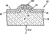
第1図Bは、アレイ1のフォトダイオードの1つ、特に、矢印hνで示される赤外線放射を受け入れる下面を有する2重層のHgCdTeヘテロジャンクション・フォトダイオード10の断面図が示されている。所望であればフォトダイオード10はホモジャンクション型デバイスとすることもできる。フォトダイオード10は入射する放射(incident radiation)を吸収して電荷担体を発生するベース層12を含んでいる。放射吸収ベース層はp形またはn形いずれの半導体材料でもよく、p−n接合部15を形成するための逆の型の導電性を持ったキャップ層14を有する。従って、放射吸収ベース層12がp形のHgCdTeであればキャップ層14はn形のHgCdTeである。IR放射の吸収により発生した電荷担体によりp−n接合部15を通って電流が流れ、この電流が読取り回路(readout circuit;図示されていない)により検出され、フォトダイオード10に結合される。
例えば、ベース層12はp形とすることができ、ヒ素を用いて約5×10¹⁵原子/cm3から約5×1016原子/cm3の濃度になるようにドーピングしてもよい。キャップ層14は本来のn形でもよければインジウムでドーピングして約1016から1017原子/cm3の濃度とすることもできる。
本発明の1つの実施例によれば、少なくともフォトダイオード10のp−n接合部15の領域は比較的薄いテルル化カドミウム(CdTe)のエピタキシャル層16でパッシベート(不動態化する;passivate)することができ、このパッシベーション層とも言えるエピタキシャル層16は通常約5000オングストロームの厚さを持っている。
本発明のもう1つの実施例によれば、パッシベーション層16はテルル化カドミウム亜鉛(Cd(1-y)ZnyTe)のエピタキシャル層からなり、この厚さもまた通常約5000オングストロームとすることができる。
本発明の更にもう1つの実施例によれば、パッシベーション層16はHg(1-x)CdxTeのエピタキシャル層からなり、xの値はそのエピタキシャル層が下に重なるベース層12及びキャップ層14よりもそれぞれ幅の広いハンドギャップを持つように選ばれる。
上述した本発明の好ましい実施例においては、ベース層12及びキャップ層14、そしてまたパッシベーション層16も、周期表第II−VI族の半導体部材、即ちそれぞれHg(1-x)CdxTe及びCdTeもしくはCd(1-y)ZnyTeである。パッシベーション層16が1つのエピタキシャル層成長法により選択的に形成される限り、p−n接合部15とパッシベーション層16間の境界にはヘテロストラクチャが形成される。即ち、パッシベーション層16の結晶質構造は本質的に下に重なるベース層及びキャップ層の結晶質構造と連続であり下層の材料よりも広いバンドギャップを有する。この結晶質の連続性は、通常0.1から0.3eVのエネルギ・ギャップを有するHgCdTe層、12及び14のバンドギャップ構造をパッシベーション層16のより広いバンドギャップへと連続的に広げて行くのに有利にはたらく。
例えば、CdTeは約1.6eVのバンド・ギャップを持っている。これにより伝導帯(conduction Band)を上向きに曲げることになり、そのためHgCdTeとCdTeの境界から電子を弾き出す。このより広いバンドギャップのため、更に価電子帯(valence band)を下向きに曲げることになり、これにより正孔(hole)を境界から弾き出す。このことは第2図に示されており、更に詳細にこれから説明する。
再び第1図Bについて触れると、ダイオード10はSi3N4、SiO2またはZnSなどの適当な誘電材料でできたガラス被覆層18を設けることができる。ガラス被覆層18は金属接点20を隣接ダイオードの同種の接点から電気的に絶縁する。金属接点20はHgCdTeキャップ層14へのオーミック接触(ohmic contact)を形成させる目的に使える任意の適切な材料で作ることができる。金属接点20の金属はキャップ層14内にあまり拡散しないことが望ましい。金属接点20に適切な金属はパラジウム及びチタンである。
エピタキシャルCdTeパッシベーション層16の固有抵抗(intrinsic resistance)が十分に高く、フォトダイオードのアレイ内の隣接するフォトダイオード同志の側方短絡(lateral shunting)を起こすことはないので、ガラス被覆層18を設けることは随意でよいことが分かっている。しかし、ガラス被覆層18の存在は、それが下層のHgCdTeベース層12及びキャップ層14それぞれからのHgの外方拡散への更なる障壁として役立つという点で、あった方が有用であることも分かっている。このガラス被覆バリアーは、接点の金属化自体によりもたらされる拡散障害とともに、Hgの外方拡散を低減するのに役立つので、得られるフォトダイオード構造は従来のデバイスよりも高温に耐えることができる。
この点については、典型的な処理(processing)及び格納(storage)温度におけるエピタキシャル・パッシベーション層16の結晶質構造はHgCdTe層からのHgの外方拡散への1次的障壁であり、ガラス被覆層18及び金属接点20により与えられる付加的な障壁はパッシベーション層16の障壁を補強するのに役立つことに留意しなければならない。また、パッシベーション層16の結晶構造の機械的特性が従来のパッシベーション・コーティングより優れているので、多孔性及び接着性の欠如に関連する問題点が克服されることにも留意しなければならない。
第2図に関しては、より広いバンドギャップのパッシベーション層16がCdTeからなり、より狭いバンドギャップの材料はHgCdTeベース層12またはHgCdTeキャップ層14を構成する第1図のフォトダイオード10の理想化したエネルギ・バンド・ダイアグラム(diagram)が示されている。見れば分かるように、伝導帯及び価電子帯におけるポテンシャル・エネルギの変化は連続的であり伝導帯は上向きに曲がり価電子帯は下向きに曲がっている。このため電子と正孔はともにそれぞれHgCdTeとCdTeとの境界から弾き出される。そうでなければ比較的高密度の格子の転位と不純物により表面状態発生電流が過大となり電荷担体の使用寿命が短くなるこの電子と正孔双方の境界からの弾き出し(repulsion)のため、この発明にかかるフォトダイオードは従来のSiO2でパッシベートされたフォトダイオードよりも優れた性能を示す。
更に、所望であればCdTeパッシベーション層16の上面はCdTe面上の電荷を下に重なるHgCdTe面から絶縁するためドープしてもよい。第2図のダイアグラムにおいて、CdTeパッシベーション層16の上面はn−形の不純物でドープされている。所望であればその代りにp−形の不純物を使うこともできる。パッシベーション層16の上面の代表的なドーピング濃度の値は約1017原子/cm3である。
例えばCd(1-y)ZnyTeをエピタキシャル面パッシベーション材料として利用することは、パッシベーション層及び下に重なるHgCdTe層を格子適合させてHgCdTeとCdZnTeの境界における転位(dislocation)を最小限に止めることができるという付加的な利点がある。例えば、yは約0.4の値となるように選ぶことができる。CdTeでパッシベートしたフォトダイオードに関して既に述べたようにCdZnTeパッシベーションの固有抵抗のためガラス被覆層18を設けることは任意でよい。
パッシベーション層16は気相エピタキシ(vaper phase epitaxy:VPE)法によりフォトダイオード上に所望の厚さにエピタキシャル成長させることができるが、勿論真空槽内で加熱した基板に、蒸気圧の高い金属の有機化合物の蒸気を送ってその金属膜を基板に成長させる方法(metalorganic chemical vapor deposition:MOCVD)などのいくつかの他の適切なエピタキシャル層形成法を用いてもよい。一般に、パッシベーション層16の結晶配列(crystalline order)がその下に重なるHgCdTeの結晶配列と同じ配列を結果的に繰り返すような方法であればどのようなエピタキシャル成長法を使っても差し支えない。パッシベーション層16が成長した後、デバイスは通常の方法で処理しガラス被覆層18及び金属接点20を堆積させることができる。エピタキシャル・パッシベーション層16の成長中に適当なマスク(mask)を用いて、接点の金属化(contact metallization)を行うべきキャップ層14の表面部分上に生じるエピ層(epilayer)の成長を阻止することができる。望ましくは、キャップ層14の全表面上にパッシベーション層を成長させ、得られたパッシベーション層は、次の処理工程で金属化部分から一部を選択的に除去した方がよい。
フォトダイオード、ゲートされ及びゲートされない可変面積フォトダイオード(gated and ungated variable area photodiode)及びMIS・コンデンサの5行5列アレイからなり、当該フォトダイオードはLWIRとMWIR双方に対するHgCdTe放射吸収材料から構成される試験用構造物(test structure)が製作された。これらの試験用構造物のうちいくつかは、従来法によるSiO2パッシベーション層を設け、一方、他のものにはエピタキシャル成長させたCdTeパッシベーション層を設けた。更に、他のいくつかの試験用構造物には、同じHgCdTeウェーハ(wafer)の上にCdTeと従来のSiO2の双方を用いたパッシベーション層を設けた。
第4、5、6、及び7図は本発明による周期表第II−VI族の元素からなるエピタキシャルパッシベーション層16を用いたフォトダイオード・デバイスの性能改善を裏付けるグラフ及び性能曲線を示す。
以上述べたように、本発明にかかる好ましい実施形態の数々を説明した。当業者であれば前述の開示に基づき上記の好ましい実施例の数々についてそれぞれ一部変更を加えることが可能である。例えば、ここに示す実施例は後方照射のメサ型光起電性放射検出器に関連して説明したが、この発明の教示内容は前方照射放射及びプラナー・タイプ・フォトダイオードにも適用され、一般にあらゆる型の周期表第II−VI族元素からなる光起電性(photovoltaic)及び光伝導性(photoconductive)デバイスに適用される。従って、本発明はここに示した実施例に限定されるものではなく、請求項に述べた範囲に限定されるものと理解されるべきものである。
【図面の簡単な説明】
第1図Aは、本発明による周期表第II−VI族の材料からなるエピタキシャル・パッシベーション層5を有する周期表第II−VI族元素からなるのフォトダイオード2のアレイ1の一部分を、縮尺通りではない様式化した斜視図である。
第1図Bは、HgCdTe放射吸収ベース層12、HgCdTeキャップ層14及びCdTe、CdZnTeまたはHgCdTeパッシベーション層16を有するフォトダイオード10の断面図である。
第2図は、第1図Bのエピタキシャル・パッシベートされたフォトダイオードの代表的なエネルギー・バンドギャップ・ダイアグラムである。
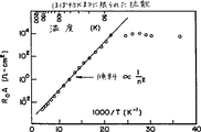
第3図Aから第3図Dまでは、CdTeパッシベートされたLWIR HgCdTeフォトダイオードの性能曲線であり、IからVまでの代表的曲線はそれぞれ80KにおけるRo A対温度、スペクトル応答、及びノイズ・スペクトルを示す。
第4図Aから第4図Dまでは、従来の技術によりSiOパッシベートされたLWIR HgCdTeフォトダイオードの性能曲線である。
第5図A及び第5図Bは、いずれも同じHgCdTeウェーハの異なる部分から製作され、それぞれのウエーハの上にCdTeパッシベートされたMWIRフォトダイオード及び従来のSiO法によりパッシベートされたMWIRフォトダイオードについての電流−電圧曲線の比較を示す。
第6図Aから第6図Cまでは、温度の関数としての、100℃におけるCdTe及び従来のSiO2それぞれについてのHgCdTeフォトダイオードのLWIR大面積、小面積、及び5×5アレイに対するそれぞれのRA積の比較を示す。
第7図A及び第7図Bは、表面再結合速度(surface recombination velocity:SRV)の100℃における焼き付け時間の関数としてのCdTeパッシベートされたフォトダイオード及び従来のSiO法によりパッシベートされたフォトダイオードそれぞれについての比較を示す。(Industrial application fields)
The present invention relates to infrared (IR) photodiodes made of materials of the Synchronous Group II-VI, and in particular, HgCdTe having a wide bandgap passivation layer (eg, made of CdTe or CdZnTe) that is epitaxially grown. The present invention relates to an IR photodiode made of a material.
(Prior art and problems to be solved by the invention)
Photodiodes composed of mercury-cadmium-tellurium (Hg (1-x) Cd x Te, where x is essentially a value from 0 to 1.0) are usually fabricated as a two-dimensional array, Covered with a passivated layer, the passivation layer consists of low temperature photochemical SiO 2 , evaporated ZnS, or anodically grown CdS. Suitable for certain imaging applications, but at some subsequent processing stage of the array, a high vacuum at 100 ° C is used to degas the vacuum Dewar containing the photodiode array. A baking cycle is required, which is considered disadvantageous with conventional passivation layers. For example, significant figure of merit degradation has been observed, such as leakage current, diode impedance, quantum efficiency, noise (especially at low frequencies), spectral response, and optical fields. This deterioration is particularly remarkable in the long wave detector. The porosity of the passivation layer and poor adhesion to the underlying HgCdTe surface are also commonly encountered problems with the conventional passivation layers described above.
Furthermore, since these conventional passivation materials do not make more than one coating on the HgCdTe surface, it is difficult or impossible to adjust the band structure and energy level at the boundary between the HgCdTe surface and the passivation layer. It is. Thus, if the array should maintain the desired figure of merit level, especially during and after high temperature processing and storage, creating flatband conditions at the interface between the HgCdTe surface and the passivation layer; It is necessary to maintain this together.
(Means for solving the problem)
The above problems are overcome by the array of IR photodiodes and similar structures according to the method and apparatus of the present invention, and other advantages are realized. That is, according to the present invention, the material has a first region that absorbs radiation and generates charge carriers from the absorbed radiation, and the radiation absorbing region is a material of Group II-VI in the periodic table having the first type conductivity. The second region is also composed of a periodic table group II-VI material having conductivity opposite to that of the first region to form a pn diode junction, and at least the first region A third region overlying the pn diode junction at the boundary between the first and second regions, the third region being composed of an epitaxial layer made of Group II-VI material of the periodic table, It has a method and apparatus for forming heterostructures with materials. The band gaps of the first and second regions may or may not be the same, and the third region has a wider band gap than either of the first and second regions.
According to an embodiment of the present invention, the third region is composed of CdTe, CdZnTe, or an epitaxial passivation layer made of HgCdTe having a wide band gap. It is lattice-matched to Group II-VI semiconductor materials in the periodic table. Optionally, a glass coating layer (overglass layer) may be provided on the passivation layer. This glass coating layer supplements the effect of an epitaxial passivation layer that prevents out-diffusion of Hg during exposure to high temperatures and electrically isolates the contacts of the photodiodes.
The foregoing and other features of the present invention will become more apparent upon reading the following detailed description of the embodiments together with the accompanying drawings.
(Example)
Here, as an example of the present invention, a back-illuminated mesa-type photovoltaic radiation detector will be described. However, the present invention relates to a photoconductive and forward-illuminated radiation detector. Also applies. The invention also applies to both homo and heterojunction devices. The present invention further includes a plurality of regions of opposite type conductivity, i.e., "wells", in which the base layer is formed in the upper surface, and pn at the boundary between the base layer and each region. It also includes a planar type detector in which a diode junction is formed.
Referring first to FIG. 1a, a stylized elevational view of an
FIG. 1B shows a cross-sectional view of one of the photodiodes in
For example, the
According to one embodiment of the invention, at least the region of the pn junction 15 of the
According to another embodiment of the present invention,
According to yet another embodiment of the present invention, the
In the preferred embodiment of the present invention described above, the
For example, CdTe has a band gap of about 1.6 eV. As a result, the conduction band is bent upward, so that electrons are ejected from the boundary between HgCdTe and CdTe. Because of this wider band gap, the valence band will be bent further downward, thereby expelling holes from the boundary. This is illustrated in FIG. 2 and will be described in further detail.
Referring again to FIG. 1B, the
The epitaxial
In this regard, the crystalline structure of the
With respect to FIG. 2, the wider
Further, if desired, the upper surface of the
For example, the use of Cd (1-y) Zn y Te as an epitaxial surface passivation material minimizes dislocation at the boundary between HgCdTe and CdZnTe by lattice matching the passivation layer and the underlying HgCdTe layer. There is an additional advantage of being able to. For example, y can be selected to have a value of about 0.4. It is optional to provide a
The
It consists of a photodiode, a gated and ungated variable area photodiode, and a 5-by-5 array of MIS capacitors, which are composed of HgCdTe radiation absorbing material for both LWIR and MWIR. A test structure was produced. Some of these test structures were provided with conventional SiO 2 passivation layers, while others were provided with epitaxially grown CdTe passivation layers. In addition, several other test structures were provided with a passivation layer using both CdTe and conventional SiO 2 on the same HgCdTe wafer.
FIGS. 4, 5, 6, and 7 show graphs and performance curves that support the performance improvement of photodiode devices using an
As described above, a number of preferred embodiments according to the present invention have been described. Those skilled in the art can make some modifications to each of the above preferred embodiments based on the foregoing disclosure. For example, although the embodiments shown herein have been described with reference to back-illuminated mesa photovoltaic radiation detectors, the teachings of the present invention also apply to front-illuminated radiation and planar type photodiodes, Applies to all types of photovoltaic and photoconductive devices consisting of Group II-VI elements of the Periodic Table. Accordingly, it is to be understood that the invention is not limited to the embodiments shown, but is limited to the scope described in the claims.
[Brief description of the drawings]
FIG. 1A shows, on a reduced scale, a portion of an
FIG. 1B is a cross-sectional view of a
FIG. 2 is a representative energy bandgap diagram of the epitaxial passivated photodiode of FIG. 1B.
FIGS. 3A through 3D are performance curves for CdTe passivated LWIR HgCdTe photodiodes, with typical curves from I to V representing Ro A vs. temperature, spectral response, and noise spectrum at 80 K, respectively. Indicates.
FIGS. 4A to 4D are performance curves of LWIR HgCdTe photodiodes that are SiO passivated according to the prior art.
FIGS. 5A and 5B are for MWIR photodiodes fabricated from different parts of the same HgCdTe wafer and CdTe passivated on each wafer and MWIR photodiodes passivated by conventional SiO methods. A comparison of current-voltage curves is shown.
FIGS. 6A to 6C show the LWIR large area, small area, and respective RA for 5 × 5 arrays of HgCdTe photodiodes for CdTe and conventional SiO 2 respectively at 100 ° C. as a function of temperature. Shows product comparison.
FIGS. 7A and 7B show CdTe passivated photodiodes as a function of baking time at 100 ° C. for surface recombination velocity (SRV) and photodiodes passivated by the conventional SiO method, respectively. The comparison about is shown.
Claims (14)
吸収されたIR放射から電荷担体を発生するためにIR放射を受容する面を持つ放射吸収性の第1の層を有し、該放射吸収層は第1のタイプの導電性を有する周期表第II−VI族の材料から構成され、
上記第1の層の上面に重なる複数のメサ領域を有し、各該メサ領域もまた上記第1の層とは逆のタイプの導電性を有する周期表第II−VI族の材料から構成され、これにより上記複数のメサ領域の各々と上記第1の層の間にある境界領域にp−nダイオード接合部を形成し、
少なくとも上記境界領域に重なるパッシベーション層を有し、該パッシベーション層は、上記境界領域とヘテロ構造を形成するのに使用しうる、周期表第II−VI族の材料のエピタキシャル層を含み、
上記第1の層及び上記複数のメサ領域はそれぞれ第1及び第2のエネルギー・バンドギャップを有し、この場合上記パッシベーション層は上記第1及び第2のエネルギー・バンドギャップのいずれか一方よりも広い第3のエネルギー・バンドギャップを有することを特徴とする、
IR放射感応フォトダイオードのアレイ。In IR radiation sensitive photodiodes,
A radiation-absorbing first layer having a surface for receiving IR radiation for generating charge carriers from the absorbed IR radiation, the radiation-absorbing layer having a first type of conductivity in the periodic table; Composed of II-VI group materials,
A plurality of mesa regions overlying the upper surface of the first layer, and each mesa region is also made of a material of Group II-VI of the periodic table having conductivity opposite to that of the first layer. This forms a pn diode junction in the boundary region between each of the plurality of mesa regions and the first layer,
Having a passivation layer overlying at least the boundary region, the passivation layer comprising an epitaxial layer of a material of Group II-VI of the periodic table that can be used to form a heterostructure with the boundary region;
The first layer and the plurality of mesa regions have first and second energy band gaps, respectively. In this case, the passivation layer is more than one of the first and second energy band gaps. Having a wide third energy band gap,
An array of IR radiation sensitive photodiodes.
第1のタイプの導電性と第1のエネルギー・バンドギャップを有する周期表第II−VI族の材料からなる第1の領域、及び上記第1の領域の上面に重なる複数のメサ領域を有する第2のタイプの導電性と第2のエネルギー・バンドギャップを有する周期表第II−VI族の材料からなる第2の領域から構成され、第2の領域は第1の領域と接触して第1及び第2の領域間の境界にp−nダイオード接合部を形成するフォトダイオードを準備すること、
少なくとも第1及び第2の領域間の境界面にわたり第1及び第2のエネルギー・バンドギャップのいずれか一方よりも広い第3のエネルギー・バンドギャップを有する周期表第II−VI族の材料からなるエピタキシャル層を成長させ、これにより少なくともそのp−nダイオード接合部をより広いバンドギャップを有するエピタキシャル層の下に位置させること、
の各段階からなることを特徴とする周期表第II−VI族の材料からなるフォトダイオードのパッシベーション法。In a method of passivating a photodiode made of a material of Group II-VI of the periodic table, the method comprises:
A first region made of Group II-VI material of the periodic table having a first type conductivity and a first energy band gap, and a plurality of mesa regions overlying the top surface of the first region . The second region is composed of a Group II-VI material of the periodic table having two types of conductivity and a second energy band gap, and the second region is in contact with the first region and is in contact with the first region. And providing a photodiode forming a pn diode junction at the boundary between the second regions,
It consists of a material of Group II-VI of the periodic table having a third energy band gap wider than either one of the first and second energy band gaps over at least the interface between the first and second regions Growing an epitaxial layer, thereby positioning at least its pn diode junction below the epitaxial layer having a wider band gap;
A method for passivation of a photodiode made of a material of Group II-VI of the periodic table.
Priority Applications (1)
| Application Number | Priority Date | Filing Date | Title |
|---|---|---|---|
| JP80002189A JP3676802B2 (en) | 1989-06-28 | 1989-06-28 | Epitaxial passivation of infrared detectors made of materials from groups (2) to (6) of the periodic table |
Applications Claiming Priority (1)
| Application Number | Priority Date | Filing Date | Title |
|---|---|---|---|
| JP80002189A JP3676802B2 (en) | 1989-06-28 | 1989-06-28 | Epitaxial passivation of infrared detectors made of materials from groups (2) to (6) of the periodic table |
Publications (2)
| Publication Number | Publication Date |
|---|---|
| JP2003273388A JP2003273388A (en) | 2003-09-26 |
| JP3676802B2 true JP3676802B2 (en) | 2005-07-27 |
Family
ID=29195496
Family Applications (1)
| Application Number | Title | Priority Date | Filing Date |
|---|---|---|---|
| JP80002189A Expired - Lifetime JP3676802B2 (en) | 1989-06-28 | 1989-06-28 | Epitaxial passivation of infrared detectors made of materials from groups (2) to (6) of the periodic table |
Country Status (1)
| Country | Link |
|---|---|
| JP (1) | JP3676802B2 (en) |
Families Citing this family (1)
| Publication number | Priority date | Publication date | Assignee | Title |
|---|---|---|---|---|
| JP2007214191A (en) * | 2006-02-07 | 2007-08-23 | Sumitomo Heavy Ind Ltd | Radiation detector and radiographic examination equipment |
-
1989
- 1989-06-28 JP JP80002189A patent/JP3676802B2/en not_active Expired - Lifetime
Also Published As
| Publication number | Publication date |
|---|---|
| JP2003273388A (en) | 2003-09-26 |
Similar Documents
| Publication | Publication Date | Title |
|---|---|---|
| US6657194B2 (en) | Multispectral monolithic infrared focal plane array detectors | |
| US3508126A (en) | Semiconductor photodiode with p-n junction spaced from heterojunction | |
| US5936268A (en) | Epitaxial passivation of group II-VI infrared photodetectors | |
| US5880510A (en) | Graded layer passivation of group II-VI infrared photodetectors | |
| Bajaj et al. | Molecular beam epitaxial HgCdTe material characteristics and device performance: reproducibility status | |
| US5401986A (en) | Bake-stable HgCdTe photodetector with II-VI passivation layer | |
| US4956304A (en) | Buried junction infrared photodetector process | |
| US4961098A (en) | Heterojunction photodiode array | |
| US20140217540A1 (en) | Fully depleted diode passivation active passivation architecture | |
| Piotrowski et al. | Extension of longwavelength IR photovoltaic detector operation to near room-temperatures | |
| US4746620A (en) | Lateral P-I-N photodetector | |
| Rutkowski | Planar junction formation in HgCdTe infrared detectors | |
| Piotrowski et al. | A novel multi-heterojunction HgCdTe long-wavelength infrared photovoltaic detector for operation under reduced cooling conditions | |
| US5599733A (en) | Method using cadmium-rich CdTe for lowering the metal vacancy concentrations of HgCdTe surfaces | |
| US4004342A (en) | Fabrication of ion implanted P-N junction devices | |
| JP3676802B2 (en) | Epitaxial passivation of infrared detectors made of materials from groups (2) to (6) of the periodic table | |
| Alchalabi et al. | Monolithic heteroepitaxial PbTe-on-Si infrared focal plane array with 96× 128 pixels | |
| Wang et al. | HgCdTe/CdTe heterostructure diodes and mosaics | |
| KR100422294B1 (en) | Passivation of HgCdTe Junction Diode By Annealing In Cd/Hg Atmosphere | |
| US5466953A (en) | Denuded zone field effect photoconductive detector | |
| Arias et al. | Molecular beam epitaxy (MBE) HgCdTe flexible growth technology for the manufacturing of infrared photovoltaic detectors | |
| WO2022245515A1 (en) | Aluminum nitride passivation layer for mercury cadmium telluride in an electrical device | |
| IL108589A (en) | SINGLE LAYER PLANAR Hg Cd Te PHOTOVOLTAIC INFRARED DETECTOR WITH HETEROSTRUCTURE PASSIVATION AND P-ON-N HOMOJUNCTION | |
| US4914495A (en) | Photodetector with player covered by N layer | |
| Riley et al. | HgCdTe hybrid focal-plane arrays |
Legal Events
| Date | Code | Title | Description |
|---|---|---|---|
| A601 | Written request for extension of time |
Free format text: JAPANESE INTERMEDIATE CODE: A601 Effective date: 20040203 |
|
| A602 | Written permission of extension of time |
Free format text: JAPANESE INTERMEDIATE CODE: A602 Effective date: 20040310 |
|
| A521 | Written amendment |
Free format text: JAPANESE INTERMEDIATE CODE: A523 Effective date: 20040506 |
|
| A131 | Notification of reasons for refusal |
Free format text: JAPANESE INTERMEDIATE CODE: A131 Effective date: 20040706 |
|
| A601 | Written request for extension of time |
Free format text: JAPANESE INTERMEDIATE CODE: A601 Effective date: 20041005 |
|
| A602 | Written permission of extension of time |
Free format text: JAPANESE INTERMEDIATE CODE: A602 Effective date: 20041129 |
|
| A521 | Written amendment |
Free format text: JAPANESE INTERMEDIATE CODE: A523 Effective date: 20050106 |
|
| TRDD | Decision of grant or rejection written | ||
| A01 | Written decision to grant a patent or to grant a registration (utility model) |
Free format text: JAPANESE INTERMEDIATE CODE: A01 Effective date: 20050405 |
|
| A61 | First payment of annual fees (during grant procedure) |
Free format text: JAPANESE INTERMEDIATE CODE: A61 Effective date: 20050502 |
|
| R150 | Certificate of patent or registration of utility model |
Free format text: JAPANESE INTERMEDIATE CODE: R150 |
|
| FPAY | Renewal fee payment (event date is renewal date of database) |
Free format text: PAYMENT UNTIL: 20090513 Year of fee payment: 4 |
|
| FPAY | Renewal fee payment (event date is renewal date of database) |
Free format text: PAYMENT UNTIL: 20090513 Year of fee payment: 4 |
|
| FPAY | Renewal fee payment (event date is renewal date of database) |
Free format text: PAYMENT UNTIL: 20100513 Year of fee payment: 5 |
|
| EXPY | Cancellation because of completion of term | ||
| FPAY | Renewal fee payment (event date is renewal date of database) |
Free format text: PAYMENT UNTIL: 20100513 Year of fee payment: 5 |