JP3676276B2 - Semiconductor device and manufacturing method thereof - Google Patents
Semiconductor device and manufacturing method thereof Download PDFInfo
- Publication number
- JP3676276B2 JP3676276B2 JP2001295292A JP2001295292A JP3676276B2 JP 3676276 B2 JP3676276 B2 JP 3676276B2 JP 2001295292 A JP2001295292 A JP 2001295292A JP 2001295292 A JP2001295292 A JP 2001295292A JP 3676276 B2 JP3676276 B2 JP 3676276B2
- Authority
- JP
- Japan
- Prior art keywords
- film
- silicide film
- silicide
- semiconductor layer
- gate electrode
- Prior art date
- Legal status (The legal status is an assumption and is not a legal conclusion. Google has not performed a legal analysis and makes no representation as to the accuracy of the status listed.)
- Expired - Fee Related
Links
Images


Description
【0001】
【発明の属する技術分野】
本発明は、半導体装置の製造方法に関し、特に金属をシリサイド化させてなるシリサイド層を形成する方法に関するものである。
【0002】
【従来の技術】
近年、半導体装置の微細化・高集積化につれて、MIS型半導体装置のゲート電極や拡散層の低抵抗化を図るための方法として、コバルト(Co),チタン(Ti),タングステン(W)などの金属膜を用いて自己整合的にゲート電極や拡散層にシリサイド膜を形成する,いわゆるサリサイドプロセスがよく知られている。以下、従来のサリサイドプロセスを用いた半導体装置の製造方法について説明する。
【0003】
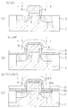
図10(a)〜図10(e)は、従来例のサリサイドプロセスを用いた半導体装置の製造工程を示す断面図である。
【0004】
まず、図10(a)に示す工程で、半導体基板101に活性領域を囲むトレンチ型の素子分離用絶縁膜102を形成した後、半導体基板101の活性領域上にシリコン酸化膜からなるゲート絶縁膜103を形成する。その後、基板上にポリシリコン膜を堆積した後、リソグラフィ及びドライエッチングにより、ポリシリコン膜をパターニングして、ゲート絶縁膜103上にゲート電極104を形成する。その後、ゲート電極104および素子分離用絶縁膜102をマスクとして活性領域に低濃度の不純物イオンを注入して、LDD領域105をゲート電極104に対して自己整合的に形成する。その後、基板上にCVD法によって酸化膜を堆積し、この酸化膜をエッチバックすることにより、ゲート電極104の側面上に酸化膜からなるサイドウォール106を形成する。その後、ゲート電極104、サイドウォール106および素子分離用絶縁膜102をマスクとして活性領域に高濃度の不純物イオンを注入して、高濃度ソース・ドレイン領域107をゲート電極104に対して自己整合的に形成する。
【0005】
次に、図10(b)に示す工程で、スパッタリング法により、基板上に、コバルト膜108を堆積した後、コバルト膜108上に窒化チタン膜109を堆積する。
【0006】
次に、図10(c)に示す工程で、窒素ガス雰囲気中で、半導体基板101に400〜500℃程度の温度で第1の短時間熱処理(RTA)を施し、ゲート電極104及び高濃度ソース・ドレイン領域107の露出している部分においてシリコン(Si)とコバルト(Co)とを反応させてコバルトリッチな第1のコバルトシリサイド膜110a(CoSiとCo2 Siとの混合体)を形成する。このとき、コバルト膜108のうちサイドウォール106及び素子分離用絶縁膜102などの絶縁膜上に位置する部分はシリサイド化されることはなく、未反応のままのコバルト膜108aが残存する。
【0007】
次に、図10(d)に示す工程で、硫酸と過酸化水素水の混合液などの溶液を用いて、窒化チタン膜109及び未反応のまま残存するコバルト膜108aを選択的に除去することによって、ゲート電極104及び高濃度ソース・ドレイン領域107上に多結晶体の第1のコバルトシリサイド膜110aを選択的に残置させる。
【0008】
次に、図10(e)に示す工程で、窒素ガス雰囲気中で、半導体基板101を800〜900℃程度の温度で第2の短時間熱処理(RTA)を行い、第1のコバルトシリサイド膜110aを構造的に安定な第2のコバルトシリサイド膜110b(CoSi2 膜)に変換する。この結果、第2のコバルトシリサイド膜110bのシート抵抗は第1のコバルトシリサイド膜110aのシート抵抗よりも小さくなり、ゲート電極104及び高濃度ソース・ドレイン領域107の低抵抗化を図ることができる。
【0009】
【発明が解決しようとする課題】
しかしながら、上述のような従来のサリサイドプロセスを用いた半導体装置の製造方法においては、シリサイド膜の凝集による影響を受けやすく、シリサイド膜の抵抗値が高抵抗化するという不具合があった。ゲート電極やソース・ドレイン領域の上に、シリサイド化反応によって形成されたコバルトシリサイドの結晶粒は、650℃以上の熱処理を受けると凝集するという性質を有する。そのため、安定なコバルトシリサイド膜を形成するために必要な第2の短時間熱処理(800〜900℃)を行なうと、結晶粒の凝集によって、コバルトシリサイド膜の一部が破断したり、極端に薄くなるという現象が見られた。
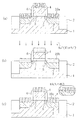
【0010】
図11(a),(b)は、それぞれ図10(c),(e)の工程における半導体装置の形状を示す断面図である。図11(a)に示すように、第1の短時間熱処理後に未反応なコバルト膜を除去して形成したコバルトシリサイド膜110aは、比較的小さな粒径を有する多くの結晶が連続した厚みのほぼ均一な1つの膜となっている。しかしながら、図11(b)に示すように、第2の短時間熱処理によってコバルト結晶粒が凝集して合体し各結晶の粒径が増大することによって、部分的に膜厚が極端に薄くなって第2のコバルトシリサイド膜110bの厚みの均一性が失われたり、第2のコバルトシリサイド膜110bの分断部分111が生じてコバルトシリサイド膜の連続性が失われることがある。その結果、第2のコバルトシリサイド膜110bの導電性が悪化し抵抗値が大幅に増大するため、ゲート電極104及び高濃度ソース・ドレイン領域107の低抵抗化が難しくなってきている。
【0011】
このようなシリサイド膜中の結晶粒の凝集の原因は以下のように考えられる。コバルトシリサイド膜が650℃以上の温度になると、各結晶粒中のコバルト原子が表面拡散をし始め、このコバルト原子の移動に応じて界面エネルギーが最小になるように、各結晶粒が移動する流動化が生じて全体の構造が変化する。つまり、結晶方位の近い複数の結晶粒同士が合体して1つの結晶粒になったり、ある結晶粒が粒界部分を取り込んで大きな結晶粒に成長するなど、結晶粒の凝集が生じると考えられている。
【0012】
特に、最近では、ゲート長が0.1μm程度になるなどゲート電極,配線などの寸法が細線化されているので、上述のような凝集が生じると抵抗値の増大だけでなくシリサイド配線の断線をも引き起こすおそれがある。また、最近では、ソース・ドレイン領域もシャロー化されて浅くなっていることから、結晶粒の凝集による部分的な結晶粒の粗大化などが生じると、シリサイド膜の一部がPN接合部に極端に近づくことによって接合リークが増大するおそれもある。
【0013】
本発明の目的は、シリサイド膜中の結晶粒の凝集による結晶粒の粗大化,不均一化を抑制する手段を講ずることにより、低抵抗で信頼性の高いシリサイド膜を有する半導体装置及びその製造方法を提供することである。
【0014】
【課題を解決するための手段】
本発明の第1の半導体装置の製造方法は、一部がシリサイド化された部材を備えた半導体装置の製造方法であって、基板の半導体層の上に金属膜を形成する工程(a)と、第1の熱処理により、上記金属膜と上記半導体層との間でシリサイド化反応を起こさせて、上記半導体層の上に多結晶構造の第1のシリサイド膜を形成する工程(b)と、上記工程(b)の後、上記金属膜の未反応部を除去する工程(c)と、上記第1のシリサイド膜内に不純物イオンを注入して、上記第1のシリサイド膜をアモルファス構造の第2のシリサイド膜に変える工程(d)と、第2の熱処理により、上記第2のシリサイド膜をアモルファス構造から多結晶構造の第3のシリサイド膜に変えて、該第3のシリサイド膜を上記部材の少なくとも一部とする工程(e)とを含み、上記工程(d)では、上記第1のシリサイド膜下の上記半導体層内まで上記不純物イオンを注入して、上記半導体層の表面部をアモルファス化する方法である。
【0015】
この方法により、第1のシリサイド膜がいったんアモルファス状態の第2のシリサイド膜になった時点で多結晶構造が破壊されるので、その後成長した第3のシリサイド膜中の結晶粒は第1のシリサイド膜の結晶粒とは独立に新たに成長したものである。したがって、第3のシリサイド膜中の結晶粒の凝集による粗大化を抑制することができ、分断部分のない厚みがほぼ均一な連続したシリサイド膜を有する半導体装置を形成することができる。そして、工程(d)では、上記半導体層内まで上記不純物イオンを注入して、上記半導体層の表面部をアモルファス化することにより、第3のシリサイド膜の結晶粒がより均一に成長するので、半導体層がゲート電極である場合にはゲート抵抗をより小さくすることができ、半導体層がソース・ドレイン領域である場合にはスパイク反応が抑制され接合リークの小さい半導体装置が得られる。
【0016】
上記半導体層を、MISFETのゲート電極の一部とし、上記工程(a)の前に、ポリシリコン膜を堆積する工程と、上記工程(a)の前又は後に、上記半導体層となる上記ゲート電極を形成する工程とをさらに含むことにより、断線のない低抵抗化されたゲート電極を有するMISFETを形成することができる。
【0017】
上記半導体層を、MISFETのソース・ドレイン領域の一部とし、上記工程(a)の前に、上記半導体層を含む活性領域の上に、ゲート絶縁膜及びゲート電極を形成する工程と、上記ゲート電極の側面上に絶縁体サイドウォールを形成する工程と、上記活性領域のうち上記ゲート電極の両側方に位置する領域に上記半導体層となるソース・ドレイン領域を形成する工程とをさらに含むことにより、ソース・ドレイン領域にゲート電極に対して自己整合的にシリサイド層を設けることができる。
【0018】
上記工程(c)の後で上記工程(d)の前に、基板上に保護膜を形成する工程をさらに含み、上記工程(d)では、上記保護膜越しに上記シリサイド膜にイオン注入を行なうことにより、保護膜によるシリサイド結晶粒の流動を抑制する機能がさらに付加されるので、より確実に上述の効果を発揮することができる。
【0019】
その場合、上記保護膜を形成する工程は、上記シリサイド膜が凝集しない温度で行なわれることが好ましい。
【0020】
また、上記保護膜を形成する工程は、上記第1の熱処理時の温度以下の温度で行なわれることが好ましい。
【0021】
上記工程(d)では、上記不純物イオンとしてシリコンイオンを用いることにより、シリサイド化反応によるシリコンの消費を補うことができ、スパイク反応の要請効果がより顕著に発揮される。
【0022】
本発明の第2の半導体装置の製造方法は、一部がシリサイド化された部材を備えた半導体装置の製造方法であって、基板の半導体層の上に第1の金属膜を形成する工程(a)と、第1の熱処理により、上記第1の金属膜と上記半導体層との間でシリサイド化反応を起こさせて、上記半導体層の上に金属リッチな第1のシリサイド膜を形成する工程(b)と、上記工程(b)の後、上記第1の金属膜の未反応部を除去する工程(c)と、上記工程(c)の後、基板上に上記第1の金属膜よりも薄い第2の金属膜を堆積する工程(d)と、上記工程(d)の後、上記第2の金属膜が形成された状態で、上記第1の熱処理よりも温度の高い第2の熱処理を行うことにより、上記第1のシリサイド膜がシリコンリッチな構造に変化した部分と、上記第2の金属膜がシリサイド化された部分とからなる第2のシリサイド膜を形成し、該第2のシリサイド膜を上記部材の少なくとも一部とする工程(e)とを含み、上記第1の熱処理は、400〜500℃の温度で行い、上記第2の熱処理は、800〜900℃の温度で行う方法である。
【0023】
この方法により、第2の金属膜が第1の金属膜よりも薄いことで、第2の金属膜のうち半導体層と接していない領域へのシリサイド膜の侵入による短絡などの不具合は回避される。
【0024】
本発明の第3の半導体装置の製造方法は、基板の半導体層の上に第1の金属膜を形成する工程(a)と、第1の熱処理により、上記第1の金属膜と上記半導体層との間でシリサイド化反応を起こさせて、上記半導体層の上に金属リッチな第1のシリサイド膜を形成する工程(b)と、上記工程(b)の後、上記第1の金属膜の未反応部を除去する工程(c)と、第2の熱処理により、上記第1のシリサイド膜をシリコンリッチな第2のシリサイド膜に変化させる工程(d)と、上記工程(d)の後、基板上に第2の金属膜を堆積する工程(e)と、第3の熱処理により、上記第2の金属膜と上記半導体層との間でシリサイド化反応を起こさせて、上記半導体層の上に金属リッチな第3のシリサイド膜を形成する工程(f)と、第4の熱処理により、上記第3のシリサイド膜をシリコンリッチな第4のシリサイド膜に変化させて、上記第2のシリサイド膜及び第4のシリサイド膜を上記部材の少なくとも一部とする工程(g)とを含み、上記第1の金属膜はチタン膜であり、上記 第2の金属膜はコバルト膜であり、上記第1のシリサイド膜及び上記第2のシリサイド膜は、チタンシリサイド膜であり、上記第3のシリサイド膜及び上記第4のシリサイド膜は、コバルトシリサイド膜である。
【0025】
この方法により、第2の熱処理において第2のシリサイド膜中で結晶粒が凝集して分断部分が生じても、第2の金属膜がシリサイド化した第4のシリサイド膜により、分断部分が補われるので、分断部分のない連続したシリサイド膜を有する半導体装置が得られる。また、第2の金属膜が第1の金属膜よりも薄いことで、第2の金属膜のうち半導体層と接していない領域へのシリサイド膜の侵入による短絡などの不具合は回避される。そして、上記工程(a)では、上記第1の金属膜としてチタン膜を形成し、上記工程(g)では、上記第2のシリサイド膜としてコバルト膜を形成することにより、反応温度の高いチタンシリサイドからなる第2のシリサイド膜中の結晶粒に影響を与えることなく、第3,第4の熱処理を行なうことができる。
【0026】
本発明の第1の半導体装置は、半導体層を有する基板と、上記半導体層の上に形成され、第1の金属のシリサイド膜と第2の金属のシリサイド膜とを一体化してなるシリサイド層とを備え、上記第1の金属のシリサイド膜は、チタンシリサイド膜であり、上記第2の金属のシリサイド膜は、コバルトシリサイド膜であり、上記第1の金属のシリサイド膜には、結晶粒の凝集による分断部分があり、上記第2の金属のシリサイド膜は、少なくとも上記第1の金属のシリサイド膜の分断部分に形成されている。
【0027】
これにより、第2のシリサイド膜中の結晶粒が凝集していても、第4のシリサイド膜によって凝集による結晶粒の存在部位の偏り,例えば分断部分や薄膜化した部分などが補われるので、比較的厚みが均一な連続したシリサイド層が得られる。上記第1の金属のシリサイド膜がチタンシリサイド膜であり、上記第2の金属のシリサイド膜がコバルトシリサイド膜であることにより、シリサイド化反応温度の相違を利用して、製造の容易化を図ることができる。
【0028】
上記半導体層及び上記シリサイド層とによって、MISFETのゲート電極や、ソース・ドレイン領域を構成することができる。
【0029】
【発明の実施の形態】
以下、本発明の実施形態について、図面を参照しながら説明する。
【0030】
(第1の実施形態)
図1(a)〜図1(c)及び図2(a)〜図2(c)は、本発明の第1の実施形態の半導体装置の製造工程を示す断面図である。
【0031】
まず、図1(a)に示す工程で、p型の半導体基板1に活性領域を囲むトレンチ型の素子分離用絶縁膜2を形成した後、半導体基板1の活性領域上にシリコン酸化膜からなるゲート絶縁膜3を形成する。その後、基板上にポリシリコン膜を堆積した後、リソグラフィ及びドライエッチングにより、ポリシリコン膜をパターニングして、ゲート絶縁膜3上にゲート電極4を形成する。その後、ゲート電極4および素子分離用絶縁膜2をマスクとして活性領域にn型の低濃度の不純物イオンを注入して、LDD領域5をゲート電極4に対して自己整合的に形成する。その後、CVD法によって基板上に酸化膜を堆積し、この酸化膜をエッチバックすることにより、ゲート電極4の側面上に酸化膜からなるサイドウォール6を形成する。その後、ゲート電極4,サイドウォール6および素子分離用絶縁膜2をマスクとして活性領域にn型の高濃度の不純物イオンを注入して、高濃度ソース・ドレイン領域7をゲート電極4に対して自己整合的に形成する。
【0032】
この工程において、高濃度ソース・ドレイン領域7に注入した不純物の活性化を行った後で、図2(b)に示す砒素イオンの注入に代えて、窒素イオン(N+ 又はN2 +)の注入を行なっても、シリサイド膜の凝集(agglomeration )に起因するシリサイド膜の分断や大きな凹凸の発生などを抑制することができる。
【0033】
また、窒素のイオン注入を行なう代わりに、コバルト膜のスパッタリングの前処理であるプリクリーン処理を行なう際に、窒素を含む雰囲気中でプラズマを発生させて、窒素プラズマをゲート電極4や高濃度ソース・ドレイン領域7に導入してもよい。このプリクリーン処理は、一般には、Arイオンを下地層に照射して下地層中の物質の逆スパッタリングを行なう処理である。シリサイドプロセス前においては、このプリクリーン処理は、シリサイド層が形成される半導体層(ゲート電極4や高濃度ソース・ドレイン領域7)表面の酸化膜除去を目的として行なわれる。
【0034】
次に、図1(b)に示す工程で、スパッタリング法により、基板上に厚み約8nmのコバルト膜8を堆積した後、コバルト膜8の上に、保護膜として厚み約20nmの窒化チタン膜9を堆積する。
【0035】
この工程において、窒化チタン膜9の堆積の前又は後で、図2(b)に示す砒素イオンの注入に代えて、窒素イオン(N+ 又はN2 +)の注入を行なっても、シリサイド膜の凝集(agglomeration )に起因するシリサイド膜の分断や大きな凹凸の発生などを抑制することができる。
【0036】
次に、図1(c)に示す工程で、窒素ガス雰囲気中で、半導体基板1に400〜500℃程度の温度で60秒程度の第1の短時間熱処理(RTA)を施して、ゲート電極4及び高濃度ソース・ドレイン領域7の露出している部分においてシリコン(Si)とコバルト(Co)とを反応させてコバルトリッチな第1のコバルトシリサイド膜10a(Co2 SiとCoSiとの混合体)を形成する。この第1のシリサイド膜10aは、微結晶の集合体になっていると考えられており、実際に図1(c)に示すような明瞭な結晶粒界が常に現れるわけではない。このとき、コバルト膜8のうちサイドウォール6及び素子分離用絶縁膜2などの絶縁膜上に位置する部分はシリサイド化されることはなく、未反応のままのコバルト膜8aが残存する。なお、第1の短時間熱処理は、窒素ガス雰囲気中の代わりに真空中やアルゴン雰囲気中で行ってもよい。
【0037】
この工程において、図2(b)に示す砒素イオンの注入に代えて、砒素イオン(As+ )の注入又は窒素イオン(N+ 又はN2 +)の注入を行なっても、シリサイド膜の凝集(agglomeration )に起因するシリサイド膜の分断や大きな凹凸の発生などを抑制することができる。
【0038】
次に、図2(a)に示す工程で、硫酸と過酸化水素水の混合液などの溶液を用いて、窒化チタン膜9及び未反応のまま残存するコバルト膜8aを選択的に除去することによって、ゲート電極4及び高濃度ソース・ドレイン領域7上に多結晶体の第1のコバルトシリサイド膜10aを選択的に残置させる。
【0039】
次に、図2(b)に示す工程で、n型の不純物イオン例えばヒ素イオン(As+ )をドーズ量1×10¹⁴atoms /cm2 程度の条件で第1のコバルトシリサイド膜10a内に注入して、少なくとも第1のコバルトシリサイド膜10aをアモルファス化してアモルファス構造の第2のコバルトシリサイド膜10bとする。このとき、第1のコバルトシリサイド膜10aの下方に位置するゲート電極4及び高濃度ソース・ドレイン領域7の表面部にも、後の第2の短時間熱処理でコバルトシリサイド膜に変換される深さまでイオン注入して、ポリシリコン又はシリコンをアモルファス化しておくことが好ましい。
【0040】
また、この工程において、砒素イオンに代えて、窒素イオン(N+ 又はN2 +)の注入を行なっても、シリサイド膜の凝集(agglomeration )に起因するシリサイド膜の分断や大きな凹凸の発生などを抑制することができる。このとき、窒素イオンとしてN+ よりもN2 +を用いた方が、シリサイド膜及び下地のポリシリコン又はシリコンをアモルファス化せさやすく,好ましい。
【0041】
次に、図2(c)に示す工程で、窒素ガス雰囲気中で、半導体基板1に800〜900℃程度の温度で10秒程度の第2の短時間熱処理(RTA)を施して、アモルファス構造の第2のコバルトシリサイド膜10bを構造的に安定な多結晶構造の第3のコバルトシリサイド膜10c(CoSi2 )に変える。なお、第2の短時間熱処理は、窒素ガス雰囲気中の代わりに真空中やアルゴン雰囲気中で行ってもよい。
【0042】
なお、上述した図1(c)又は図2(b)の工程で砒素イオンの注入を行なった場合には、図2(c)に示すように、第3のコバルトシリサイド膜10cは、横方向に粒界がほとんどないいわゆるバンブー構造を有しているが、上記砒素イオン注入の代わりに、図1(a),図1(b),図1(c)及び図2(b)に示す工程のうちのいずれかの工程で窒素イオンを注入した場合には、図2(c)の右上に示すように、横方向に粒界のある多結晶体になり、結晶粒が重なったほぼ積層構造となる。
【0043】
図14(a),(b)は、窒素イオンの注入を行なって形成されたシリサイド層の明視野及び暗視野のTEM写真図である。図14(c),(d)は、従来の窒素イオンの注入を伴わないシリサイド膜の明視野及び暗視野のTEM写真図である。図14(a)〜(d)は、N2 イオンを、加速エネルギー20keV,ドーズ量1×10¹⁵・cm-2の条件で、ソース・ドレイン領域の不純物活性化のためのアニールの後に、第1のコバルトシリサイド膜に注入して得られた第3のコバルトシリサイド膜の構造を示している。
【0044】
図14(a),(b)に示すように、窒素イオンを注入することにより、いわゆるバンブー構造ではなく横方向に粒界のある,つまり多結晶体の積層構造を有するシリサイド膜が形成されている。また、グレインサイズが小さく、CoSi2 粒が上下に積層されている。さらに、コバルトシリサイド膜の上面はスムーズである。つまり、熱処理によって、上層のCoSi2 粒界に下層のCoSi2 粒が入り込み、下層のCoSi2 膜には凝集(アグロメレーション)が生じていない。
【0045】
それに対し、図14(c),(d)に示すように、窒素イオンの注入を伴わずに形成されたコバルトシリサイド膜は、いわゆるバンブー構造であり、横方向に粒界がない。また、グレインサイズが大きく、アグロメレーションが発生している。さらに、コバルトシリサイド膜の上面や、コバルトシリサイド膜−下地層間の界面がラフである。
【0046】
本実施形態の製造工程によると、図2(b)に示す工程で、多結晶構造の第1のコバルトシリサイド膜10aに砒素イオンの注入を行い、第1のコバルトシリサイド膜10aをアモルファス構造の第2のコバルトシリサイド膜10bにした後に、図2(c)に示す工程で、第2の短時間熱処理により多結晶構造の第3のコバルトシリサイド膜10cを形成するため、従来の製造工程のように第2の短時間熱処理によって結晶粒の凝集を生じることなく、アモルファス構造の第2のコバルトシリサイド膜10bの全領域がほぼ均一な多結晶からなる安定な第3のコバルトシリサイド膜10cに変換する。従って、最終的に形成されるコバルトシリサイド膜10cに部分的な分断は生じにくく、厚みが均一で連続的な1つの膜である第3のコバルトシリサイド膜10cを形成することができる。したがって、ゲート電極4や高濃度ソース・ドレイン領域7の低抵抗化を確実に実現することができる。また、ゲート電極やゲート配線が細線化された場合でも、一部が断線するような事態を回避することができ、高濃度ソース・ドレイン領域7がシャロー化されても、比較的均一な結晶粒径による均一な厚みのシリサイド膜が得られることで、接合リークを抑制することができる。
【0047】
また、第1のコバルトシリサイド膜10aへのイオン注入の際に、第1のコバルトシリサイド膜10aの下方に位置するゲート電極4及び高濃度ソース・ドレイン領域7の表面部までアモルファス化しておくことによって、第2の短時間熱処理の際に第3のコバルトシリサイド膜10cの結晶粒が均一に成長する。したがって、ゲート電極4の低抵抗化をより効果的に実現することができるとともに、高濃度ソース・ドレイン領域7の下方においてスパイク反応が起こりにくくなって、接合リーク異常を抑制することができる。
【0048】
なお、上記実施形態では、図2(b)に示す工程で、ヒ素をイオン注入して第1のコバルトシリサイド膜10aをアモルファス構造に変化させたが、ヒ素の代わりにシリコン(Si)をイオン注入してアモルファス化してもよい。このようにシリコンをイオン注入した場合には、第2の短時間熱処理の反応におけるゲート電極4及び高濃度ソース・ドレイン領域7のシリコンの消費を補うことができるので、スパイク反応による接合リークを抑制することができる。この結果、第3のコバルトシリサイド膜10cのシート抵抗が下がり、ゲート電極4及び高濃度ソース・ドレイン領域7の低抵抗化を図ることができる。あるいは、砒素の代わりに、アルゴン(Ar),ゲルマニウム(Ge),すず(Sn)などの電気的に中性で第1のコバルトシリサイド膜10aをアモルファス化することができる元素を注入してもよい。この場合、砒素イオンの注入と同様に、シリサイド膜の凝集に起因するシリサイド膜の分断や大きな凹凸の発生などを抑制することができる。
【0049】
また、ソース・ドレイン領域上のシリサイド膜にキャリア発生用のドーパントとなる不純物をイオン注入する場合は、当該ソース・ドレイン領域の導電型と同じ導電型の不純物を注入する方が好ましい。例えば、ソース・ドレイン領域がp型の場合には、ガリウム(Ga)又はインジウム(In)を注入し、ソース・ドレイン領域がn型の場合には、砒素(As)又はアンチモン(Sb)を注入する。デュアルゲート構造を有するゲート電極上のシリサイド膜にイオン注入する場合にも同様である。
【0050】
ここで、砒素イオンの注入を行なうタイミングは、図2(c)に示す工程に限定されるものではなく、図1(c)に示す工程であってもよい。
【0051】
また、砒素イオンに代えて、図1(a)又は(b)に示す工程で(つまり、第1のコバルトシリサイド膜10aを形成する前に)窒素を半導体層(ゲート電極4又は高濃度ソース・ドレイン領域7)のうちシリサイド膜が形成される部分に導入することができる。また、図1(b)又は図2(b)に示す工程で、窒素を半導体層(ゲート電極4又は高濃度ソース・ドレイン領域7)に導入することもできる。
【0052】
窒素イオンを注入した場合には、第2の短時間熱処理によって、図2(c)の右上や図14に示す多結晶体の積層構造が現れる。その場合、第2の短時間熱処理を行なっても、従来のようなコバルトシリサイド結晶粒の凝集が生じにくいことが確認されている。よって、分断部分のない厚みがほぼ均一な連続したシリサイド膜を有するMISトランジスタを形成することができる。したがって、ゲート電極4及び高濃度ソース・ドレイン領域7の低抵抗化を図ることができる。
【0053】
その理由は完全に解明されているわけではないが、例えば以下の機構が考えられる。図2(c)の右上に示す多結晶体の積層構造の場合、横方向に生じている粒界でその上下の結晶中の原子の拡散が互いに逆向きになることで拡散が妨害されたり、窒素が存在することで原子の拡散自体が抑制される結果、凝集が妨げられるものと考えることができる。結晶の凝集は、各結晶粒中の金属原子やシリコン原子などの原子がある方向(例えば時計回り)に拡散することで、結晶粒の表面積を減少させる駆動力が生じることによると考えることもできるからである。
【0054】
そして、シリサイド膜中に窒素を導入する場合には、砒素を導入する場合のごとく半導体層のキャリア濃度に与える影響が少ないという利点がある。
【0055】
図12は、従来の方法によるシリサイド膜(窒素注入なし)を有するMISFETと、窒素イオン(N2 +)を導入したシリサイド膜を有するMISFETとの接合リークを測定した結果を示す図である。ここでは、窒素イオンを加速エネルギー20keV,ドーズ量1×10¹⁵・cm-2の条件で注入している。同図に示すように、シリサイド膜に窒素を導入しない従来の方法によって形成されたMISトランジスタにおいては、接合リークに大きなバラツキがあるのに対し、窒素が導入されたシリサイド膜を有するMISトランジスタにおいては、接合リーク値のバラツキも小さいことがわかる。この結果、CoSi2 膜の形成温度やこの工程以降の熱処理温度を650℃〜700℃程度にしても接合リークの増大が生じない。したがって、トランジスタのショートチャネル特性を悪化させることなく、700℃程度で熱処理を行なうことができる。
【0056】
その場合、窒素イオンの注入条件を、N2 ドーズ量2×10¹⁴〜2×10¹⁵・cm-2の範囲で行なうことが好ましい。ドーズ量が2×10¹⁴・cm-2未満であると、シリサイド結晶の凝集を抑制する効果が十分得られず、ドーズ量が2×10¹⁵・cm-2を越えると、CoSi2 /Si界面における界面抵抗が増大するからである。
【0057】
また、導入された窒素はシリサイド膜だけではなく半導体層(本実施形態では、ゲート電極4,高濃度ソース・ドレイン領域7,LDD領域5など)にも導入されてしまうが、シリサイド膜以外の半導体層(ゲート電極4,高濃度ソース・ドレイン領域7及びLDD領域5)における窒素の濃度は、第3のコバルトシリサイド膜10cを形成した後で、1×1017cm-3以下であることが好ましい。言い換えると、1×1017cm-3を越える窒素を含む領域は、シリサイド膜だけに限定することが好ましい。窒素濃度が高いと、半導体層中の不純物(砒素,リン,ボロンなど)の活性化が十分に行われないおそれがあり、その結果、MISトランジスタのドレイン電流が低下したり、ゲート電極,ゲート配線の抵抗が過度に増大することがあるからである。
【0058】
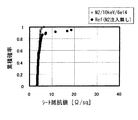
図13は、ゲート電極,ゲート配線などのシート抵抗の窒素の有無による相違を示すデータである。同図に示すように、窒素を導入していない場合には、相当の確率でシート抵抗値の大きいサンプルが出現している。それに対して、加速エネルギー10keV,ドーズ量6×10¹⁴・cm-2の条件で窒素イオン(N2 +)の注入を行なうことにより、シート抵抗値の大きいサンプルは出現せず、安定したシート抵抗値が得られている。すなわち、本発明の効果が示されている。
【0059】
本実施形態及び後述の各実施形態において、形成するシリサイド膜は必ずしもコバルトシリサイド膜でなくてもよく、チタンシリサイド膜,タングステンシリサイド膜,ニッケルシリサイド膜,モリブデンシリサイド膜、タンタルシリサイド膜など、各種金属シリサイド膜に対して、本発明を適用することができる。ただし、コバルトシリサイド膜の場合、シリサイド化反応をチタンシリサイド膜より低温で行なわせることができるため、半導体基板内の不純物プロファイルに与える影響が少ないという利点がある。
【0060】
(第2の実施形態)
図3(a)〜図3(c)及び図4(a)〜図4(c)は、本発明の第2の実施形態の半導体装置の製造工程を示す断面図である。
【0061】
まず、図3(a)に示す工程で、p型の半導体基板1に活性領域を囲むトレンチ型の素子分離用絶縁膜2を形成した後、半導体基板1の活性領域上にシリコン酸化膜からなるゲート絶縁膜3を形成する。その後、基板上にポリシリコン膜を堆積した後、リソグラフィ及びドライエッチングにより、ポリシリコン膜をパターニングして、ゲート絶縁膜3上にゲート電極4を形成する。その後、ゲート電極4および素子分離用絶縁膜2をマスクとして活性領域にn型の低濃度の不純物イオンを注入して、LDD領域5をゲート電極4に対して自己整合的に形成する。その後、CVD法によって基板上に酸化膜を堆積し、この酸化膜をエッチバックすることにより、ゲート電極4の側面上に酸化膜からなるサイドウォール6を形成する。その後、ゲート電極4、サイドウォール6および素子分離用絶縁膜2をマスクとして活性領域にn型の高濃度の不純物イオンを注入して、高濃度ソース・ドレイン領域7をゲート電極4に対して自己整合的に形成する。
【0062】
この工程において、高濃度ソース・ドレイン領域7に注入した不純物の活性化を行った後で、図4(b)に示す砒素イオンの注入に代えて、窒素イオン(N+ 又はN2 +)の注入を行なっても、シリサイド膜の凝集(agglomeration )に起因するシリサイド膜の分断や大きな凹凸の発生などを抑制することができる。
【0063】
また、窒素のイオン注入を行なう代わりに、コバルト膜のスパッタリングの前処理であるプリクリーン処理を行なう際に、窒素を含む雰囲気中でプラズマを発生させて、窒素プラズマをゲート電極4や高濃度ソース・ドレイン領域7に導入してもよい。
【0064】
次に、図3(b)に示す工程で、スパッタリング法により、基板上に厚み約8nmのコバルト膜8を堆積した後、コバルト膜8の上に、保護膜として厚み約20nmの窒化チタン膜9を堆積する。
【0065】
この工程において、窒化チタン膜9の堆積の前又は後で、図4(b)に示す砒素イオンの注入に代えて、窒素イオン(N+ 又はN2 +)の注入を行なっても、シリサイド膜の凝集(agglomeration )に起因するシリサイド膜の分断や大きな凹凸の発生などを抑制することができる。
【0066】
次に、図3(c)に示す工程で、窒素ガス雰囲気中で、半導体基板1に400〜500℃程度の温度で60秒程度の第1の短時間熱処理(RTA)を施して、ゲート電極4及び高濃度ソース・ドレイン領域7の露出している部分においてシリコン(Si)とコバルト(Co)とを反応させてコバルトリッチな第1のコバルトシリサイド膜10a(Co2 SiとCoSiとの混合体)を形成する。この第1のシリサイド膜10aは、微結晶の集合体になっていると考えられており、実際に図3(c)に示すような明瞭な結晶粒界が常に現れるわけではない。このとき、コバルト膜8のうちサイドウォール6及び素子分離用絶縁膜2などの絶縁膜上に位置する部分はシリサイド化されることはなく、未反応のままのコバルト膜8aが残存する。なお、第1の短時間熱処理は、窒素ガス雰囲気中の代わりに真空中やアルゴン雰囲気中で行ってもよい。
【0067】
この工程において、図4(b)に示す砒素イオンの注入に代えて、砒素イオン(As+ )の注入又は窒素イオン(N+ 又はN2 +)の注入を行なっても、シリサイド膜の凝集(agglomeration )に起因するシリサイド膜の分断や大きな凹凸の発生などを抑制することができる。
【0068】
次に、図4(a)に示す工程で、硫酸と過酸化水素水の混合液などの溶液を用いて、窒化チタン膜9及び未反応のまま残存するコバルト膜8aを選択的に除去することによって、ゲート電極4及び高濃度ソース・ドレイン領域7上に多結晶体の第1のコバルトシリサイド膜10aを選択的に残置させる。その後、基板上に厚み約20nmのCVD酸化膜からなる保護膜12を堆積する。このとき、保護膜12の堆積温度は、第1のシリサイド膜が凝集する温度よりも低い温度、例えば、本実施形態のようにコバルトシリサイド膜を用いる場合は、650℃以下であることが好ましい。さらに、保護膜12の堆積温度は、第1の短時間熱処理の温度と同程度あるいはそれ以下の温度であることがより好ましい。なお、保護膜12としては、CVD酸化膜の他にプラズマ酸化膜やプラズマ窒化膜などの絶縁膜や、窒化チタン膜の導体膜を用いてもよい。
【0069】
次に、図4(b)に示す工程で、n型の不純物イオン例えばヒ素イオン(As+ )をドーズ量約1×10¹⁴atoms /cm2 の条件で第1のコバルトシリサイド膜10a内に保護膜12を通過させて注入して、少なくとも第1のコバルトシリサイド膜10aをアモルファス化してアモルファス構造の第2のコバルトシリサイド膜10bとする。このとき、第1のコバルトシリサイド膜10aの下方に位置するゲート電極4及び高濃度ソース・ドレイン領域7の表面部にも、後の第2の短時間熱処理でコバルトシリサイド膜に変換される深さまでイオン注入して、ポリシリコン又はシリコンをアモルファス化しておくことが好ましい。
【0070】
また、この工程において、砒素イオンに代えて、窒素イオン(N+ 又はN2 +)の注入を行なっても、シリサイド膜の凝集(agglomeration )に起因するシリサイド膜の分断や大きな凹凸の発生などを抑制することができる。このとき、窒素イオンとしてN+ よりもN2 +を用いた方が、シリサイド膜及び下地のポリシリコン又はシリコンをアモルファス化せさやすく,好ましい。
【0071】
次に、図4(c)に示す工程で、窒素ガス雰囲気中で、半導体基板1に800〜900℃程度の温度で10秒程度の第2の短時間熱処理(RTA)を施して、アモルファス構造の第2のコバルトシリサイド膜10bを構造的に安定な多結晶構造の第3のコバルトシリサイド膜10c(CoSi2 )に変換する。なお、第2の短時間熱処理は、窒素ガス雰囲気中の代わりに真空中やアルゴン雰囲気中で行ってもよい。
【0072】
なお、上述した図3(c)又は図4(b)の工程で砒素イオンの注入を行なった場合には、図4(c)に示すように、第3のコバルトシリサイド膜10cは、横方向に粒界がほとんどないいわゆるバンブー構造を有しているが、上記砒素イオン注入の代わりに、図3(a),図3(b),図3(c)及び図4(b)に示す工程のうちのいずれかの工程で窒素イオンを注入した場合には、図4(c)の右上に示すように、横方向に粒界のある多結晶体になり、結晶粒が重なったほぼ積層構造となる。
【0073】
その後、保護膜12が絶縁膜の場合にはそのまま残存させて、保護膜12上に層間絶縁膜を形成してもよい。また、保護膜12が窒化チタン膜のような導体膜の場合には、保護膜12を選択的に除去した後、層間絶縁膜を形成すれば良い。
【0074】
本実施形態の製造工程によると、図4(a)に示す工程で、第1のコバルトシリサイド膜10aの上に保護膜12を堆積した後、図4(b)に示す工程で、保護膜12越しに第1のコバルトシリサイド膜10aにイオン注入を行い、アモルファス構造の第2のアモルファス・コバルトシリサイド膜10bとし、図4(c)に示す工程で第2の短時間熱処理により多結晶構造の第3のコバルトシリサイド膜10cを形成するため、保護膜12によってコバルトシリサイドの結晶粒の流動化が抑制される。しかも、アモルファス状態になっているため、従来の製造工程のように第2の短時間熱処理によって結晶粒の凝集を生じることなく、アモルファス構造の第2のコバルトシリサイド膜10bの全領域がほぼ均一な多結晶からなる安定な第3のコバルトシリサイド膜10cに変換される。従って、第3のコバルトシリサイド膜10cに部分的な分断は生じにくく、厚みが均一で連続的な1つの膜である第3のコバルトシリサイド膜10cを形成することができる。したがって、ゲート電極4や高濃度ソース・ドレイン領域7の低抵抗化を確実に実現することができる。また、ゲート電極やゲート配線が細線化された場合でも、一部が断線するような事態を回避することができ、高濃度ソース・ドレイン領域7がシャロー化されても、比較的均一な結晶粒径による均一な厚みのシリサイド膜が得られることで、接合リークを抑制することができる。
【0075】
また、第1のコバルトシリサイド膜10aへのイオン注入の際に、第1のコバルトシリサイド膜10aの下方に位置するゲート電極4及び高濃度ソース・ドレイン領域7の表面部までアモルファス化しておくことによって、第2の短時間熱処理の際に第3のコバルトシリサイド膜10cの結晶粒が均一に成長する。したがって、ゲート電極4の低抵抗化をより効果的に実現することができるとともに、高濃度ソース・ドレイン領域7の下方においてスパイク反応が起こりにくくなって、接合リーク異常を抑制することができる。
【0076】
なお、上記実施形態では、図4(b)に示す工程で、ヒ素をイオン注入して第1のコバルトシリサイド膜10aをアモルファス構造にしたが、ヒ素の代わりにシリコン(Si)をイオン注入してアモルファス化してもよい。このようにシリコンをイオン注入した場合には、第2の短時間熱処理の反応におけるゲート電極4及び高濃度ソース・ドレイン領域7のシリコンの消費を補うことができるので、スパイク反応による接合リークを抑制することができる。この結果、第3のコバルトシリサイド膜10cのシート抵抗が下がり、ゲート電極4及び高濃度ソース・ドレイン領域7の低抵抗化を図ることができる。あるいは、砒素の代わりに、アルゴン(Ar),ゲルマニウム(Ge),すず(Sn)などの電気的に中性で第1のコバルトシリサイド膜10aをアモルファス化することができる元素を注入してもよい。この場合、砒素イオンの注入と同様に、シリサイド膜の凝集に起因するシリサイド膜の分断や大きな凹凸の発生などを抑制することができる。
【0077】
ここで、砒素イオンの注入を行なうタイミングは、図4(c)に示す工程に限定されるものではなく、図3(c)に示す工程であってもよい。
【0078】
窒素イオンを注入した場合には、第2の短時間熱処理によって、図4(c)の右上に示す多結晶体の積層構造が現れる。その場合、第2の短時間熱処理を行なっても、従来のようなコバルト結晶粒の凝集による合体が生じにくいことが確認されている。その理由は、第1の実施形態において既に説明した通りである。
【0079】
その場合、窒素イオンの注入条件を、ドーズ量2×10¹⁴〜2×10¹⁵・cm-2の範囲で行なうことが好ましい。ドーズ量が2×10¹⁴・cm-2以下であると、シリサイド結晶の凝集を抑制する効果が十分得られず、ドーズ量が2×1015cm-2を越えると、CoSi2 /Si界面における界面抵抗が増大するからである。
【0080】
また、導入された窒素はシリサイド膜だけではなく半導体層(本実施形態では、ゲート電極4,高濃度ソース・ドレイン領域7,LDD領域5など)にも導入されてしまうが、シリサイド膜以外の半導体層(ゲート電極4,高濃度ソース・ドレイン領域7及びLDD領域5)における窒素の濃度は、第3のコバルトシリサイド膜10cを形成した後で、1×10¹⁷・cm-3以下であることが好ましい。言い換えると、1×10¹⁷・cm-3を越える窒素を含む領域は、シリサイド膜だけに限定することが好ましい。窒素濃度が高いと、半導体層中の不純物(砒素,リン,ボロンなど)の活性化が十分に行われないおそれがあり、その結果、MISトランジスタのドレイン電流が低下したり、ゲート電極,ゲート配線のシート抵抗が過度に増大することがあるからである。
【0081】
(第3の実施形態)
図5(a)〜図5(c)及び図6(a)〜図6(c)は、本発明の第3の実施形態の半導体装置の製造工程を示す断面図である。
【0082】
まず、図5(a)に示す工程で、p型の半導体基板1に活性領域を囲むトレンチ型の素子分離用絶縁膜2を形成した後、半導体基板1の活性領域上にシリコン酸化膜からなるゲート絶縁膜3を形成する。その後、基板上にポリシリコン膜を堆積した後、リソグラフィ及びドライエッチングにより、ポリシリコン膜をパターニングして、ゲート絶縁膜3上にゲート電極4を形成する。その後、ゲート電極4および素子分離用絶縁膜2をマスクとして活性領域にn型の低濃度の不純物イオンを注入して、LDD領域5をゲート電極4に対して自己整合的に形成する。その後、CVD法によって基板上に酸化膜を堆積し、この酸化膜をエッチバックすることにより、ゲート電極4の側面上に酸化膜からなるサイドウォール6を形成する。その後、ゲート電極4、サイドウォール6および素子分離用絶縁膜2をマスクとして活性領域にn型の高濃度の不純物イオンを注入して、高濃度ソース・ドレイン領域7をゲート電極4に対して自己整合的に形成する。
【0083】
次に、図5(b)に示す工程で、スパッタリング法により、基板上に厚み約8nmのコバルト膜8を堆積した後、コバルト膜8の上に厚み約20nmの窒化チタン膜9を堆積する。
【0084】
次に、図5(c)に示す工程で、窒素ガス雰囲気中で、半導体基板1に400〜500℃程度の温度で60秒程度の第1の短時間熱処理(RTA)を施して、ゲート電極4及び高濃度ソース・ドレイン領域7の露出している部分においてシリコン(Si)とコバルト(Co)とを反応させてコバルトリッチな第1のコバルトシリサイド膜20a(Co2 SiとCoSiとの混合体)を形成する。このとき、コバルト膜8のうちサイドウォール6及び素子分離用絶縁膜2などの絶縁膜上に位置する部分はシリサイド化されることはなく、未反応のままのコバルト膜8aが残存する。なお、第1の短時間熱処理は、窒素ガス雰囲気中の代わりに真空中やアルゴン雰囲気中で行ってもよい。
【0085】
次に、図6(a)に示す工程で、硫酸と過酸化水素水の混合液などの溶液を用いて、窒化チタン膜9及び未反応のまま残存するコバルト膜8aを選択的に除去することによって、ゲート電極4及び高濃度ソース・ドレイン領域7上に多結晶構造の第1のコバルトシリサイド膜20aを選択的に残置させる。その後、スパッタリング法により、基板上に、第1のコバルトシリサイド膜20aの形成に用いた第1の金属膜であるコバルト膜8よりも膜厚の薄い第2の金属膜として厚みが約2nmのコバルト膜13を堆積した後、コバルト膜13上に連続して第2の保護膜となる厚みが約20nmの窒化チタン膜14を堆積する。
【0086】
次に、図6(b)に示す工程で、窒素ガス雰囲気中で、半導体基板1に800〜900℃程度の温度で10秒程度の第2の短時間熱処理(RTA)を施して、金属リッチな第1のコバルトシリサイド膜20aをシリコンリッチで構造的に安定な第2のコバルトシリサイド膜20b(CoSi2 )に変換する。この第2の短時間熱処理により、第1のコバルトシリサイド膜20aとその上のコバルト膜13との間ではシリサイド化反応が進行するが、コバルト膜13のうちサイドウォール6及び素子分離用絶縁膜2の上に位置する部分ではシリサイド化反応が生じず、未反応のままのコバルト膜13aが残存する。ここで、第2の短時間熱処理の温度は第1の短時間熱処理の温度に比べると高いので、第1の短時間熱処理と連続して第2の短時間熱処理を行なうと、第1の短時間熱処理の際に未反応のコバルト膜8aまでシリサイド膜が浸食して、ゲート電極4と高濃度ソース・ドレイン領域7とがシリサイド膜を介して導通するおそれがある。それに対し、本実施形態においては、第2の金属膜であるコバルト膜13は約2nmの厚みしかなく薄いので、第2の短時間熱処理によって未反応のコバルト膜13a全体がシリサイド化されることはない。なお、第2の短時間熱処理は、窒素ガス雰囲気中の代わりに真空中やアルゴン雰囲気中で行ってもよい。
【0087】
次に、図6(c)に示す工程で、硫酸と過酸化水素水の混合液などの溶液を用いて、窒化チタン膜14及び未反応のまま残存するコバルト膜13aを選択的に除去することによって、ゲート電極4及び高濃度ソース・ドレイン領域7上に第2のコバルトシリサイド膜20bを選択的に残置させることができる。
【0088】
本実施形態の製造工程によると、図6(a)に示す工程で、第1のコバルトシリサイド膜20aの上に薄いコバルト膜13を堆積した後、図6(b)に示す工程で、コバルト膜13が全面に形成されている状態で第2の短時間熱処理を行うため、第2の短時間熱処理の際にも、従来の製造工程のように第2のコバルトシリサイド膜20bに部分的な分断は生じにくく、全領域が連続している安定な第2のコバルトシリサイド膜20bが得られる。したがって、ゲート電極4や高濃度ソース・ドレイン領域7の低抵抗化を確実に実現することができる。また、ゲート電極やゲート配線が細線化された場合でも、一部が断線するような事態を回避することができ、高濃度ソース・ドレイン領域7がシャロー化されても、比較的均一な厚みのシリサイド膜が得られることで、接合リークを抑制することができる。
【0089】
なお、本実施形態においても、第2の実施形態を応用して、第2の金属膜を堆積してから不純物イオンを第1のシリサイド膜内に注入すると、より結晶粒を微細化できる効果がある。
【0090】
(第4の実施形態)
図7(a)〜図7(c)、図8(a)〜図8(c)及び図9(a)、図9(b)は、本発明の第4の実施形態の半導体装置の製造工程を示す断面図である。
【0091】
まず、図7(a)に示す工程で、p型の半導体基板1に活性領域を囲むトレンチ型の素子分離用絶縁膜2を形成した後、半導体基板1の活性領域上にシリコン酸化膜からなるゲート絶縁膜3を形成する。その後、基板上にポリシリコン膜を堆積した後、リソグラフィ及びドライエッチングにより、ポリシリコン膜をパターニングして、ゲート絶縁膜3上にゲート電極4を形成する。その後、ゲート電極4および素子分離用絶縁膜2をマスクとして活性領域にn型の低濃度の不純物イオンを注入して、LDD領域5をゲート電極4に対して自己整合的に形成する。その後、CVD法によって基板上に酸化膜を堆積し、この酸化膜をエッチバックすることにより、ゲート電極4の側面上に酸化膜からなるサイドウォール6を形成する。その後、ゲート電極4、サイドウォール6および素子分離用絶縁膜2をマスクとして活性領域にn型の高濃度の不純物イオンを注入して、高濃度ソース・ドレイン領域7をゲート電極4に対して自己整合的に形成する。
【0092】
次に、図7(b)に示す工程で、スパッタリング法により、基板上に厚み約8nmのコバルト膜8を堆積した後、コバルト膜8の上に厚み約20nmの窒化チタン膜9を堆積する。
【0093】
次に、図7(c)に示す工程で、窒素ガス雰囲気中で、半導体基板1に400〜500℃程度の温度で60秒程度の第1の短時間熱処理(RTA)を施して、ゲート電極4及び高濃度ソース・ドレイン領域7の露出している部分においてシリコン(Si)とコバルト(Co)とを反応させてコバルトリッチな第1のコバルトシリサイド膜20a(Co2 SiとCoSiとの混合体)を形成する。このとき、コバルト膜8のうちサイドウォール6及び素子分離用絶縁膜2などの絶縁膜上に位置する部分はシリサイド化されることはなく、未反応のままのコバルト膜8aが残存する。なお、第1の短時間熱処理は、窒素ガス雰囲気中の代わりに真空中やアルゴン雰囲気中で行ってもよい。
【0094】
次に、図8(a)に示す工程で、硫酸と過酸化水素水の混合液などの溶液を用いて、窒化チタン膜9及び未反応のまま残存するコバルト膜8aを選択的に除去することによって、ゲート電極4及び高濃度ソース・ドレイン領域7上に第1のコバルトシリサイド膜20aを選択的に残置させる。その後、窒素ガス雰囲気中で、半導体基板1を800〜900℃程度で第2の短時間熱処理(RTA)を行い、第1のコバルトシリサイド膜20aを構造的に安定な第2のコバルトシリサイド膜20b(CoSi2 )に変換する。このとき、第2の短時間熱処理によってコバルト原子の移動による結晶粒の凝集が生じて、結晶粒径が増大することによって部分的に膜厚が極端に薄くなったり、第2のコバルトシリサイド膜20bに分断部分15が生じてその分断部分で下地のシリコン層が露出した状態になることがある。
【0095】
次に、図8(b)に示す工程で、スパッタリング法により、基板上に第2の金属膜として厚みが約6nmのコバルト膜16を堆積した後、コバルト膜16の上に第2の保護膜として厚みが約20nmの窒化チタン膜17を堆積する。
【0096】
次に、図8(c)に示す工程で、窒素ガス雰囲気中で、半導体基板1に400〜500℃程度の温度で60秒程度の第3の短時間熱処理(RTA)を施す。この結果、ゲート電極4及び高濃度ソース・ドレイン領域7のうち第2のコバルトシリサイド膜20bの分断部分15において露出している部分のシリコン(Si)とコバルト(Co)とが反応してコバルトリッチな第3のコバルトシリサイド膜18a(Co2 SiあるいはCoSi)が形成される。このとき、第2のコバルトシリサイド膜20bとコバルト膜16との間でもシリサイド化反応が進行するが、コバルト膜16と第2のコバルトシリサイド膜20bの分断部分15におけるシリコン層との反応に比べると、反応はわずかである。なお、コバルト膜16のうちサイドウォール6及び素子分離用絶縁膜2の上に位置する部分ではシリサイド化反応が生ぜず、未反応のままのコバルト膜16aが残存する。なお、第3の短時間熱処理は、窒素ガス雰囲気中の代わりに真空中やアルゴン雰囲気中で行ってもよい。
【0097】
次に、図9(a)に示す工程で、硫酸と過酸化水素水の混合液などの溶液を用いて、窒化チタン膜17及び未反応のまま残存するコバルト膜16aを選択的に除去することによって、ゲート電極4及び高濃度ソース・ドレイン領域7の上に第2のコバルトシリサイド膜20bと共に第3のコバルトシリサイド膜18aを選択的に残置させる。
【0098】
次に、図9(b)に示す工程で、窒素ガス雰囲気中で、半導体基板1を800〜900℃程度の温度で10秒程度の第4の短時間熱処理(RTA)を行い、第3のコバルトシリサイド膜18aを構造的に安定な第4のコバルトシリサイド膜18b(CoSi2 )に変換する。なお、第4の短時間熱処理は、窒素ガス雰囲気中の代わりに真空中やアルゴン雰囲気中で行ってもよい。
【0099】
本実施形態の製造工程によると、図7(b)、図7(c)及び図8(a)に示す工程で、構造的に安定な第2のコバルトシリサイド膜20bを形成した後、図8(b)、図8(c)、図9(a)及び図9(b)に示す工程で、第2のコバルトシリサイド膜20bを形成する際に分断部分15が生じていても、最終的にはその分断部分15において構造的に安定な第4のコバルトシリサイド膜18bが形成されるため、第2のコバルトシリサイド膜20bおよび第4のコバルトシリサイド膜18bからなる連続的なシリサイド膜を形成することができる。この結果、第2,第4のコバルトシリサイド膜20b,18bからなるシリサイド膜全体のシート抵抗が小さくなり、ゲート電極4及び高濃度ソース・ドレイン領域7の低抵抗化を図ることができる。
【0100】
なお、上記実施形態では、第1,第2の金属膜のいずれもコバルト膜を用いて説明したが、第1の金属膜としてチタン膜、第2の金属膜としてコバルト膜を用いて、チタンシリサイド膜とコバルトシリサイド膜からなるシリサイド膜を形成してもよい。このとき、まずチタンシリサイド膜を形成した後、コバルトシリサイド膜を形成すれば、チタンシリサイド膜の凝集する温度がコバルトシリサイド膜に比べて高いため、チタンシリサイド膜の結晶粒径を変化させることなくシリコンが露出している分断部分にコバルトシリサイド膜を形成することができる。
【0101】
(その他の実施形態)
上記第1〜第4の実施形態において、コバルト膜上に窒化チタン膜を用いて説明したが、窒化膜や酸化膜でもよい。
【0102】
また、半導体基板として、バルクの半導体基板だけでなく、SOI基板を用いてもよく、シリコン基板以外の半導体基板であってもよい。また、例えばシリコン基板にSiGe層,SiGeC層を設けたヘテロ接合を有するものであってもよい。
【0103】
さらに、シリサイド層を形成する対象部材は、ゲート電極,ゲート配線だけでもよい。その場合、次の2つのケースが考えられる。第1の方法は、まず、ポリシリコン膜をパターニングして、ゲート電極,ゲート配線を形成してからシリサイド化処理を行なう方法である。第2の方法は、ポリシリコン膜と金属膜とを積層し、金属膜のシリサイド化を行なって第1のシリサイド膜を形成してから、ポリサイド膜をパターニングしてゲート電極,ゲート配線を形成する方法である。この第2の方法の場合、第1のシリサイド膜から本発明の第2,第3のシリサイド膜を形成する工程は、ポリサイド膜のパターニング前に行なってもよいし、ポリサイド膜のパターニング後に行なってもよい。
【0104】
また、シリサイド層を形成する対象部材は、ゲート電極,ゲート配線だけでなく,ポリシリコン配線,ポリシリコン電極(パッド)など金属のシリサイド化処理が可能な材料からなる他の部材であってもよい。例えば、DRAMメモリセルトランジスタにおいては、ゲート電極,ゲート配線(ワード線)だけにシリサイド層が設けられることがある。一般の配線,電極(パッド)においても、シリサイド結晶粒の凝集によって部分的に空隙や高抵抗部が生じると、その部材自身又はその部分に接続されるコンタクト部材との電気的接続に不具合が生じることがあるので、本発明を適用することにより、各実施形態で述べたような効果が得られる。また、キャパシタの電極や、抵抗素子の配線とのコンタクト部などにおいても同様である。
【0105】
ただし、特に微細化された部材においては、局所的なシリサイド層の空隙や薄膜化による影響が大きいので、MISFETのゲート電極,ゲート配線やソース・ドレイン領域上へのシリサイド層を形成する場合に本発明を適用する意義が大きいといえる。もちろん、その場合にも、ゲート電極,ゲート配線だけにシリサイド層を形成する工程や、ソース・ドレイン領域だけにシリサイド層を形成する工程に本発明を適用してもよいことは言うまでもない。
【0106】
また、ゲート配線の切断現象について本発明者が調べた結果、切断部近傍のシリサイド結晶(コバルトシリサイド結晶)は、CoSi2 によって構成されていることがわかった。そこで、本発明では、第2の短時間熱処理をCoSi2 結晶粒が生じにくい条件,つまり725℃以下の温度(ただし、第1の短時間熱処理温度よりも高い温度)で行なう。これにより、ゲート電極,ゲート配線などの切断(断線)を抑制することができる。
【0107】
ただし、725℃以下の低温条件で第2の短時間熱処理を行なった場合、MISトランジスタの接合リークの増大や、スパイクの発生などの不具合があり得る。そこで、第2の短時間熱処理の後で、シリサイド膜を酸化膜などの保護膜で覆ってから、第3の短時間熱処理を、例えば850℃,30secの条件で行なう。この第3の短時間熱処理は、例えば、図2(c)に示す工程の後、基板上に層間絶縁膜であるBPSG膜などを堆積してから、層間絶縁膜をリフローさせる目的で行なわれる熱処理と兼用して行なうことができる。
【0108】
これにより、ゲート電極,ゲート配線などの細線化による切断を抑制しつつ、MISトランジスタの接合リークの抑制を図ることができる。
【0109】
【発明の効果】
本発明によれば、シリサイド膜に生じる分断部分による高抵抗化を防止することができ、ゲート電極やソース・ドレイン領域が微細化されても低抵抗なシリサイド膜を有する半導体装置を形成することができる。
【図面の簡単な説明】
【図1】 (a)〜(c)は、第1の実施形態の半導体装置の製造工程のうち第1のシリサイド膜を形成するまでの工程を示す断面図である。
【図2】 (a)〜(c)は、第1の実施形態の半導体装置の製造工程のうち未反応のコバルト膜を除去してから第3のシリサイド膜を形成するまでの工程を示す断面図である。
【図3】 (a)〜(c)は、第2の実施形態の半導体装置の製造工程のうち第1のシリサイド膜を形成するまでの工程を示す断面図である。
【図4】 (a)〜(c)は、第2の実施形態の半導体装置の製造工程のうち未反応のコバルト膜を除去してから第3のシリサイド膜を形成するまでの工程を示す断面図である。
【図5】 (a)〜(c)は、第3の実施形態の半導体装置の製造工程のうち第1のシリサイド膜を形成するまでの工程を示す断面図である。
【図6】 (a)〜(c)は、第3の実施形態の半導体装置の製造工程のうち第2の金属膜,保護膜を形成してから第2のシリサイド膜を形成するまでの工程を示す断面図である。
【図7】 (a)〜(c)は、第4の実施形態の半導体装置の製造工程のうち第1のシリサイド膜を形成するまでの工程を示す断面図である。
【図8】 (a)〜(c)は、第4の実施形態の半導体装置の製造工程のうち第2のシリサイド膜を形成してから第3のシリサイド膜を形成するまでの工程を示す断面図である。
【図9】 (a)〜(c)は、第4の実施形態の半導体装置の製造工程のうち未反応の第2のコバルト膜を除去してから第4のシリサイド膜を形成するまでの工程を示す断面図である。
【図10】 (a)〜(e)は、従来のサリサイド構造を有する半導体装置の製造工程を示す断面図である。
【図11】 (a)及び(b)は、それぞれ図10(d)及び図10(e)に示す断面図の拡大図である。
【図12】 従来の方法によるシリサイド膜を有するMISFETと、窒素イオンを導入したシリサイド膜を有するMISFETとの接合リークを測定した結果を示す図である。
【図13】 ゲート電極,ゲート配線などの抵抗の窒素の有無による相違を示すデータである。
【図14】 (a),(b)は、窒素イオンの注入を行なって形成されたシリサイド層の明視野及び暗視野のTEM写真図である。(c),(d)は、従来の窒素イオンの注入を伴わないシリサイド膜の明視野及び暗視野のTEM写真図である。
【符号の説明】
1 半導体基板
2 素子分離用絶縁膜
3 ゲート絶縁膜
4 ゲート電極
5 LDD領域(低濃度ソース・ドレイン領域)
6 サイドウォール
7 高濃度ソース・ドレイン領域
8 コバルト膜
9 窒化チタン膜
10a 第1のコバルトシリサイド膜
10b 第2のコバルトシリサイド膜
10c 第3のコバルトシリサイド膜
12 保護膜
13 コバルト膜
14 窒化チタン膜
15 分断部分
16 コバルト膜
17 窒化チタン膜
18 コバルトシリサイド膜
18a 第3のコバルトシリサイド膜
18b 第4のコバルトシリサイド膜
20a 第1のコバルトシリサイド膜
20b 第2のコバルトシリサイド膜[0001]
BACKGROUND OF THE INVENTION
The present invention relates to a method for manufacturing a semiconductor device, and more particularly to a method for forming a silicide layer formed by siliciding a metal.
[0002]
[Prior art]
In recent years, with the miniaturization and high integration of semiconductor devices, as a method for reducing the resistance of gate electrodes and diffusion layers of MIS type semiconductor devices, cobalt (Co), titanium (Ti), tungsten (W), etc. A so-called salicide process in which a silicide film is formed on a gate electrode or a diffusion layer in a self-aligning manner using a metal film is well known. Hereinafter, a method of manufacturing a semiconductor device using a conventional salicide process will be described.
[0003]
FIG. 10A to FIG. 10E are cross-sectional views showing a manufacturing process of a semiconductor device using a conventional salicide process.
[0004]
First, in the step shown in FIG. 10A, a trench type element
[0005]
Next, in the step shown in FIG. 10B, a
[0006]
Next, in the step shown in FIG. 10C, the
[0007]
Next, in the step shown in FIG. 10D, the
[0008]
Next, in the step shown in FIG. 10E, the
[0009]
[Problems to be solved by the invention]
However, the conventional method for manufacturing a semiconductor device using the salicide process as described above has a problem that it is easily affected by the aggregation of the silicide film and the resistance value of the silicide film is increased. Cobalt silicide crystal grains formed by a silicidation reaction on the gate electrode and the source / drain regions have a property of aggregating when subjected to heat treatment at 650 ° C. or higher. Therefore, when the second short-time heat treatment (800 to 900 ° C.) necessary for forming a stable cobalt silicide film is performed, a part of the cobalt silicide film is broken or extremely thin due to agglomeration of crystal grains. The phenomenon of becoming was seen.
[0010]
11A and 11B are cross-sectional views showing the shape of the semiconductor device in the steps of FIGS. 10C and 10E, respectively. As shown in FIG. 11A, the
[0011]
The cause of such agglomeration of crystal grains in the silicide film is considered as follows. When the cobalt silicide film reaches a temperature of 650 ° C. or higher, the cobalt atoms in each crystal grain begin to diffuse, and each crystal grain moves so that the interfacial energy is minimized according to the movement of the cobalt atom. The entire structure changes as a result. In other words, it is thought that agglomeration of crystal grains occurs, for example, when a plurality of crystal grains having close crystal orientations are combined into one crystal grain, or a certain crystal grain takes in the grain boundary portion and grows into a large crystal grain. ing.
[0012]
In particular, since the gate electrode and wiring dimensions have been thinned recently, for example, the gate length has become about 0.1 μm, when the above aggregation occurs, not only the resistance value increases but also the silicide wiring is disconnected. May also cause. In addition, recently, the source / drain regions are also shallowed and become shallow, so that when a part of a crystal grain becomes coarse due to agglomeration of crystal grains, a part of a silicide film is extremely extended to a PN junction. There is also a possibility that junction leakage increases by approaching.
[0013]
SUMMARY OF THE INVENTION An object of the present invention is to provide a semiconductor device having a low-resistance and high-reliability silicide film and a method for manufacturing the same by taking measures to suppress coarsening and non-uniformity of crystal grains due to aggregation of crystal grains in the silicide film Is to provide.
[0014]
[Means for Solving the Problems]
A first method for manufacturing a semiconductor device according to the present invention is a method for manufacturing a semiconductor device including a partly silicided member, the step (a) of forming a metal film on a semiconductor layer of a substrate; A step (b) of causing a silicidation reaction between the metal film and the semiconductor layer by a first heat treatment to form a first silicide film having a polycrystalline structure on the semiconductor layer; After the step (b), a step (c) of removing an unreacted portion of the metal film, and an impurity ion is implanted into the first silicide film, so that the first silicide film has an amorphous structure. And changing the second silicide film from an amorphous structure to a third silicide film having a polycrystalline structure by the step (d) of changing to a second silicide film and a second heat treatment, and changing the third silicide film to the member Steps to at least part of ( ) AndIn the step (d), the impurity ions are implanted into the semiconductor layer below the first silicide film to make the surface portion of the semiconductor layer amorphous.
[0015]
By this method, the polycrystalline structure is destroyed once the first silicide film becomes the second silicide film in the amorphous state, so that the crystal grains in the third silicide film grown thereafter are the first silicide film. Newly grown independently of the crystal grains of the film. Therefore, the coarsening due to the aggregation of crystal grains in the third silicide film can be suppressed, and a semiconductor device having a continuous silicide film having a substantially uniform thickness without a parting portion can be formed.Then, in the step (d), the impurity ions are implanted into the semiconductor layer to make the surface portion of the semiconductor layer amorphous, so that the crystal grains of the third silicide film grow more uniformly. When the semiconductor layer is a gate electrode, the gate resistance can be further reduced, and when the semiconductor layer is a source / drain region, a spike reaction is suppressed and a semiconductor device with small junction leakage can be obtained.
[0016]
The semiconductor layer is a part of a gate electrode of a MISFET, a step of depositing a polysilicon film before the step (a), and a gate electrode that becomes the semiconductor layer before or after the step (a) In addition, a MISFET having a low-resistance gate electrode without disconnection can be formed.
[0017]
Forming the semiconductor layer as a part of a source / drain region of a MISFET, forming a gate insulating film and a gate electrode on the active region including the semiconductor layer before the step (a), and the gate A step of forming an insulator sidewall on the side surface of the electrode, and a step of forming source / drain regions to be the semiconductor layer in regions of the active region located on both sides of the gate electrode. A silicide layer can be provided in the source / drain region in a self-aligned manner with respect to the gate electrode.
[0018]
The method further includes a step of forming a protective film on the substrate after the step (c) and before the step (d). In the step (d), ions are implanted into the silicide film through the protective film. As a result, the function of suppressing the flow of silicide crystal grains by the protective film is further added, so that the above-described effect can be more reliably exhibited.
[0019]
In that case, the step of forming the protective film is preferably performed at a temperature at which the silicide film does not aggregate.
[0020]
Moreover, it is preferable that the process of forming the said protective film is performed at the temperature below the temperature at the said 1st heat processing.
[0021]
UpIn the step (d), the aboveImpurity ionsBy using silicon ions, the consumption of silicon due to the silicidation reaction can be supplemented, and the required effect of the spike reaction can be exhibited more remarkably.
[0022]
A second method for manufacturing a semiconductor device according to the present invention is a method for manufacturing a semiconductor device including a partly silicided member, and a step of forming a first metal film on a semiconductor layer of a substrate ( a) and a step of causing a silicidation reaction between the first metal film and the semiconductor layer by a first heat treatment to form a metal-rich first silicide film on the semiconductor layer. (B) After the step (b), after removing the unreacted portion of the first metal film (c) and after the step (c), the first metal film is formed on the substrate. Depositing a thin second metal film (d),After the step (d), the second metal film is formed and the temperature is higher than that of the first heat treatment.Second heat treatmentBy doingForming a second silicide film composed of a portion where the first silicide film is changed to a silicon-rich structure and a portion where the second metal film is silicided, and the second silicide film is formed as described above. Step (e) for forming at least part of memberThe first heat treatment is performed at a temperature of 400 to 500 ° C., and the second heat treatment is performed at a temperature of 800 to 900 ° C.
[0023]
By this method, since the second metal film is thinner than the first metal film, problems such as a short circuit due to penetration of the silicide film into a region of the second metal film that is not in contact with the semiconductor layer can be avoided. .
[0024]
According to a third method of manufacturing a semiconductor device of the present invention, the first metal film and the semiconductor layer are formed by a step (a) of forming a first metal film on a semiconductor layer of a substrate and a first heat treatment. (B) forming a metal-rich first silicide film on the semiconductor layer by performing a silicidation reaction between the first metal film and the first metal film after the process (b). After the step (c) of removing the unreacted portion, the step (d) of changing the first silicide film to the silicon-rich second silicide film by the second heat treatment, and the step (d), A step (e) of depositing a second metal film on the substrate and a third heat treatment cause a silicidation reaction between the second metal film and the semiconductor layer to form a top surface of the semiconductor layer. Forming a metal-rich third silicide film (f) and a fourth heat treatment. Ri, the third silicide film by changing the silicon-rich fourth silicide film, the second silicide layer and the fourth silicide film and step (g) to at least a portion of the memberThe first metal film is a titanium film, The second metal film is a cobalt film, the first silicide film and the second silicide film are titanium silicide films, and the third silicide film and the fourth silicide film are cobalt silicide films. Is.
[0025]
According to this method, even if crystal grains aggregate in the second silicide film in the second heat treatment and a divided portion is generated, the divided portion is supplemented by the fourth silicide film in which the second metal film is silicided. As a result, a semiconductor device having a continuous silicide film without a dividing portion can be obtained. In addition, since the second metal film is thinner than the first metal film, problems such as a short circuit due to penetration of the silicide film into a region of the second metal film that is not in contact with the semiconductor layer can be avoided.In the step (a), a titanium film is formed as the first metal film, and in the step (g), a cobalt film is formed as the second silicide film. The third and fourth heat treatments can be performed without affecting the crystal grains in the second silicide film.
[0026]
A first semiconductor device of the present invention includes a substrate having a semiconductor layer, a silicide layer formed on the semiconductor layer, and formed by integrating a first metal silicide film and a second metal silicide film; WithThe silicide film of the first metal is a titanium silicide film, the silicide film of the second metal is a cobalt silicide film, and the first metal silicide film has a divided portion due to agglomeration of crystal grains. The silicide film of the second metal is formed at least on a part of the silicide film of the first metal..
[0027]
As a result, even if the crystal grains in the second silicide film are aggregated, the fourth silicide film compensates for the deviation of the presence of crystal grains due to the aggregation, for example, a divided part or a thinned part. A continuous silicide layer having a uniform target thickness can be obtained.Since the first metal silicide film is a titanium silicide film and the second metal silicide film is a cobalt silicide film, the difference in silicidation reaction temperature is utilized to facilitate the manufacture. Can do.
[0028]
The semiconductor layer and the silicide layer can constitute a gate electrode of MISFET and source / drain regions.
[0029]
DETAILED DESCRIPTION OF THE INVENTION
Hereinafter, embodiments of the present invention will be described with reference to the drawings.
[0030]
(First embodiment)
FIG. 1A to FIG. 1C and FIG. 2A to FIG. 2C are cross-sectional views showing the manufacturing steps of the semiconductor device of the first embodiment of the present invention.
[0031]
First, in the step shown in FIG. 1A, a trench type element
[0032]
In this step, after the impurity implanted into the high-concentration source /
[0033]
Further, instead of performing ion implantation of nitrogen, when performing a preclean process, which is a pretreatment for sputtering of the cobalt film, plasma is generated in an atmosphere containing nitrogen, and the nitrogen plasma is converted into the
[0034]
Next, in the step shown in FIG. 1B, a
[0035]
In this step, before or after the deposition of the
[0036]
Next, in the step shown in FIG. 1C, the
[0037]
In this step, arsenic ions (As) are used instead of the arsenic ion implantation shown in FIG.+ ) Implantation or nitrogen ions (N+ Or N2 +) Injection can also suppress the separation of the silicide film and the occurrence of large irregularities due to the agglomeration of the silicide film.
[0038]
Next, in the step shown in FIG. 2A, the
[0039]
Next, in the step shown in FIG. 2B, n-type impurity ions such as arsenic ions (As+ )
[0040]
In this process, instead of arsenic ions, nitrogen ions (N+ Or N2 +) Injection can also suppress the separation of the silicide film and the occurrence of large irregularities due to the agglomeration of the silicide film. At this time, N as nitrogen ions+ Than N2 +Is preferable because it is easy to make the silicide film and the underlying polysilicon or silicon amorphous.
[0041]
Next, in the step shown in FIG. 2 (c), the
[0042]
When arsenic ions are implanted in the process of FIG. 1C or FIG. 2B described above, the third
[0043]
14A and 14B are TEM photographs of bright and dark fields of a silicide layer formed by implanting nitrogen ions. FIGS. 14C and 14D are TEM photographs of bright and dark fields of a conventional silicide film without nitrogen ion implantation. 14 (a) to 14 (d) show N2 Ions with acceleration energy of 20 keV and dose of 1 × 10¹⁵・
[0044]
As shown in FIGS. 14 (a) and 14 (b), by implanting nitrogen ions, a silicide film having a grain boundary in the lateral direction, that is, a polycrystalline structure, is formed instead of the so-called bamboo structure. Yes. Also, the grain size is small and CoSi2 Grains are stacked one above the other. Furthermore, the upper surface of the cobalt silicide film is smooth. That is, the upper layer of CoSi is formed by heat treatment.2 CoSi below the grain boundary2 Grain enters and the underlying CoSi2 There is no aggregation (agglomeration) in the membrane.
[0045]
On the other hand, as shown in FIGS. 14C and 14D, the cobalt silicide film formed without nitrogen ion implantation has a so-called bamboo structure and has no grain boundaries in the lateral direction. Moreover, the grain size is large and agglomeration occurs. Furthermore, the upper surface of the cobalt silicide film and the interface between the cobalt silicide film and the underlying layer are rough.
[0046]
According to the manufacturing process of the present embodiment, arsenic ions are implanted into the polycrystalline first
[0047]
Further, when ion implantation is performed on the first
[0048]
In the above embodiment, arsenic is ion-implanted in the step shown in FIG. 2B to change the first
[0049]
In addition, when an impurity serving as a dopant for generating carriers is ion-implanted into the silicide film on the source / drain region, it is preferable to implant an impurity having the same conductivity type as that of the source / drain region. For example, gallium (Ga) or indium (In) is implanted when the source / drain region is p-type, and arsenic (As) or antimony (Sb) is implanted when the source / drain region is n-type. To do. The same applies to the case where ions are implanted into a silicide film on a gate electrode having a dual gate structure.
[0050]
Here, the timing of implanting arsenic ions is not limited to the step shown in FIG. 2C, and may be the step shown in FIG.
[0051]
Further, instead of arsenic ions, nitrogen is used in the semiconductor layer (the
[0052]
When nitrogen ions are implanted, a polycrystalline multi-layer structure shown in the upper right of FIG. 2C and FIG. 14 appears by the second short-time heat treatment. In that case, it has been confirmed that even if the second short-time heat treatment is performed, the conventional aggregation of cobalt silicide crystal grains hardly occurs. Therefore, it is possible to form a MIS transistor having a continuous silicide film having a substantially uniform thickness without a parting portion. Therefore, the resistance of the
[0053]
The reason is not completely elucidated, but for example, the following mechanism can be considered. In the case of the polycrystalline layered structure shown in the upper right of FIG. 2 (c), diffusion is hindered by the reverse diffusion of atoms in the upper and lower crystals at the grain boundaries occurring in the lateral direction, As a result of the suppression of atomic diffusion itself due to the presence of nitrogen, it can be considered that aggregation is hindered. It can be considered that the aggregation of the crystal is caused by a driving force that reduces the surface area of the crystal grain by diffusing atoms such as metal atoms and silicon atoms in each crystal grain in a certain direction (for example, clockwise). Because.
[0054]
When nitrogen is introduced into the silicide film, there is an advantage that the influence on the carrier concentration of the semiconductor layer is small as in the case of introducing arsenic.
[0055]
FIG. 12 shows a conventional MISFET having a silicide film (without nitrogen implantation) and nitrogen ions (N2 +Is a diagram showing the result of measuring the junction leak with a MISFET having a silicide film introduced with a). Here, nitrogen ions are accelerated at an energy of 20 keV and a dose of 1 × 10.15・ Cm-2The condition is injected. As shown in the figure, in a MIS transistor formed by a conventional method in which nitrogen is not introduced into a silicide film, there is a large variation in junction leakage, whereas in a MIS transistor having a silicide film into which nitrogen is introduced. It can also be seen that the variation in the junction leakage value is small. As a result, CoSi2 Even if the film formation temperature or the heat treatment temperature after this step is about 650 ° C. to 700 ° C., junction leakage does not increase. Therefore, heat treatment can be performed at about 700 ° C. without deteriorating the short channel characteristics of the transistor.
[0056]
In that case, the nitrogen ion implantation condition is N2 Dose amount 2 × 10¹⁴~ 2x10¹⁵・ Cm-2It is preferable to carry out within the range. Dose amount is 2 × 10¹⁴・ Cm-2If it is less than 1, the effect of suppressing the agglomeration of silicide crystals cannot be sufficiently obtained, and the dose amount is 2 × 10.15・ Cm-2Exceeds CoSi2 This is because the interface resistance at the / Si interface increases.
[0057]
Further, the introduced nitrogen is introduced not only into the silicide film but also into the semiconductor layer (in this embodiment, the
[0058]
FIG. 13 is data showing the difference in sheet resistance between the gate electrode and the gate wiring depending on the presence or absence of nitrogen. As shown in the figure, when nitrogen is not introduced, a sample having a large sheet resistance value appears with a considerable probability. On the other hand,
[0059]
In this embodiment and each embodiment described later, the silicide film to be formed is not necessarily a cobalt silicide film, and various metal silicides such as a titanium silicide film, a tungsten silicide film, a nickel silicide film, a molybdenum silicide film, and a tantalum silicide film are used. The present invention can be applied to a film. However, in the case of a cobalt silicide film, the silicidation reaction can be performed at a lower temperature than the titanium silicide film, and thus has an advantage that the influence on the impurity profile in the semiconductor substrate is small.
[0060]
(Second Embodiment)
FIG. 3A to FIG. 3C and FIG. 4A to FIG. 4C are cross-sectional views showing the manufacturing steps of the semiconductor device of the second embodiment of the present invention.
[0061]
First, in the step shown in FIG. 3A, a trench type element
[0062]
In this step, after the impurity implanted into the high concentration source /
[0063]
Further, instead of performing ion implantation of nitrogen, when performing a preclean process, which is a pretreatment for sputtering of the cobalt film, plasma is generated in an atmosphere containing nitrogen, and the nitrogen plasma is converted into the
[0064]
3B, a
[0065]
In this step, before or after the deposition of the
[0066]
Next, in the step shown in FIG. 3C, the
[0067]
In this step, arsenic ions (As) are used instead of the arsenic ion implantation shown in FIG.+ ) Implantation or nitrogen ions (N+ Or N2 +) Injection can also suppress the separation of the silicide film and the occurrence of large irregularities due to the agglomeration of the silicide film.
[0068]
Next, in the step shown in FIG. 4A, the
[0069]
Next, in the step shown in FIG. 4B, n-type impurity ions such as arsenic ions (As+ ) Dose of about 1 × 10¹⁴atoms / cm2 Under the above conditions, the
[0070]
In this process, instead of arsenic ions, nitrogen ions (N+ Or N2 +) Injection can also suppress the separation of the silicide film and the occurrence of large irregularities due to the agglomeration of the silicide film. At this time, N as nitrogen ions+ Than N2 +Is preferable because it is easy to make the silicide film and the underlying polysilicon or silicon amorphous.
[0071]
Next, in the step shown in FIG. 4C, the
[0072]
When arsenic ions are implanted in the above-described step of FIG. 3C or FIG. 4B, the third
[0073]
Thereafter, when the
[0074]
According to the manufacturing process of the present embodiment, after the
[0075]
Further, when ion implantation is performed on the first
[0076]
In the above embodiment, arsenic is ion-implanted in the step shown in FIG. 4B to form the first
[0077]
Here, the timing of implanting arsenic ions is not limited to the step shown in FIG. 4C, and may be the step shown in FIG.
[0078]
When nitrogen ions are implanted, a polycrystalline laminated structure shown in the upper right of FIG. 4C appears by the second short-time heat treatment. In that case, it has been confirmed that even if the second short-time heat treatment is performed, coalescence due to agglomeration of cobalt crystal grains as in the conventional case hardly occurs. The reason is as already described in the first embodiment.
[0079]
In that case, the implantation condition of nitrogen ions is set to a dose amount of 2 × 10.14~ 2x10¹⁵・ Cm-2It is preferable to carry out within the range. Dose amount is 2 × 10¹⁴・ Cm-2If it is below, the effect of suppressing the agglomeration of silicide crystals cannot be sufficiently obtained, and the dose amount is 2 × 1015cm-2Exceeds CoSi2 This is because the interface resistance at the / Si interface increases.
[0080]
Further, the introduced nitrogen is introduced not only into the silicide film but also into the semiconductor layer (in this embodiment, the
[0081]
(Third embodiment)
FIG. 5A to FIG. 5C and FIG. 6A to FIG. 6C are cross-sectional views showing the manufacturing steps of the semiconductor device of the third embodiment of the present invention.
[0082]
First, in the step shown in FIG. 5A, a trench type element
[0083]
Next, in the step shown in FIG. 5B, a
[0084]
Next, in the step shown in FIG. 5C, the
[0085]
Next, in the step shown in FIG. 6A, the
[0086]
Next, in the step shown in FIG. 6B, the
[0087]
Next, in the step shown in FIG. 6C, the
[0088]
According to the manufacturing process of this embodiment, after depositing the
[0089]
Also in this embodiment, by applying the second embodiment and depositing the second metal film and then implanting impurity ions into the first silicide film, there is an effect that the crystal grains can be further refined. is there.
[0090]
(Fourth embodiment)
FIG. 7A to FIG. 7C, FIG. 8A to FIG. 8C, FIG. 9A and FIG. 9B show the manufacture of the semiconductor device of the fourth embodiment of the present invention. It is sectional drawing which shows a process.
[0091]
First, in the step shown in FIG. 7A, a trench type element
[0092]
Next, in the step shown in FIG. 7B, a
[0093]
Next, in the step shown in FIG. 7C, the
[0094]
Next, in the step shown in FIG. 8A, the
[0095]
Next, in the step shown in FIG. 8B, after depositing a
[0096]
Next, in the step shown in FIG. 8C, a third short-time heat treatment (RTA) is performed on the
[0097]
Next, in the step shown in FIG. 9A, the
[0098]
Next, in the step shown in FIG. 9B, the
[0099]
According to the manufacturing process of the present embodiment, after forming the structurally stable second
[0100]
In the above embodiment, both the first and second metal films have been described using a cobalt film. However, a titanium film is used as the first metal film, a cobalt film is used as the second metal film, and titanium silicide is used. A silicide film made of a film and a cobalt silicide film may be formed. At this time, if the titanium silicide film is first formed and then the cobalt silicide film is formed, the temperature at which the titanium silicide film aggregates is higher than that of the cobalt silicide film. A cobalt silicide film can be formed in the divided portion where the is exposed.
[0101]
(Other embodiments)
In the first to fourth embodiments, the titanium nitride film is used on the cobalt film, but a nitride film or an oxide film may be used.
[0102]
Further, as the semiconductor substrate, not only a bulk semiconductor substrate but also an SOI substrate may be used, and a semiconductor substrate other than a silicon substrate may be used. Further, for example, it may have a heterojunction in which a SiGe layer and a SiGeC layer are provided on a silicon substrate.
[0103]
Further, the target member for forming the silicide layer may be only the gate electrode and the gate wiring. In that case, the following two cases can be considered. The first method is a method of first performing a silicidation process after patterning a polysilicon film to form a gate electrode and a gate wiring. In the second method, a polysilicon film and a metal film are stacked, the metal film is silicided to form a first silicide film, and then the polycide film is patterned to form a gate electrode and a gate wiring. Is the method. In the case of this second method, the step of forming the second and third silicide films of the present invention from the first silicide film may be performed before the patterning of the polycide film or after the patterning of the polycide film. Also good.
[0104]
The target member for forming the silicide layer is not limited to the gate electrode and the gate wiring, but may be another member made of a material capable of silicidation of metal such as a polysilicon wiring or a polysilicon electrode (pad). . For example, in a DRAM memory cell transistor, a silicide layer may be provided only on the gate electrode and the gate wiring (word line). Even in general wiring and electrodes (pads), if gaps or high resistance portions are partially generated due to agglomeration of silicide crystal grains, there is a problem in electrical connection with the members themselves or contact members connected to the portions. Therefore, by applying the present invention, the effects described in the embodiments can be obtained. The same applies to the electrode of the capacitor and the contact portion with the wiring of the resistance element.
[0105]
However, particularly in a miniaturized member, the influence of local voids or thinning of the silicide layer is large, so this is necessary when forming a silicide layer on the gate electrode, gate wiring, source / drain region of the MISFET. It can be said that the significance of applying the invention is great. Of course, in this case, it goes without saying that the present invention may be applied to a process of forming a silicide layer only on the gate electrode and the gate wiring, and a process of forming a silicide layer only on the source / drain regions.
[0106]
In addition, as a result of the present inventors examining the cutting phenomenon of the gate wiring, the silicide crystal (cobalt silicide crystal) in the vicinity of the cut portion is CoSi.2 It was found that it is configured by. Therefore, in the present invention, the second short-time heat treatment is performed using CoSi.2 The conditions are such that crystal grains are not easily generated, that is, a temperature of 725 ° C. or lower (however, a temperature higher than the first short-time heat treatment temperature). Thereby, cutting | disconnection (disconnection) of a gate electrode, gate wiring, etc. can be suppressed.
[0107]
However, when the second short-time heat treatment is performed under a low temperature condition of 725 ° C. or lower, there may be problems such as an increase in junction leakage of the MIS transistor and occurrence of spikes. Therefore, after the second short-time heat treatment, the silicide film is covered with a protective film such as an oxide film, and then the third short-time heat treatment is performed under conditions of, for example, 850 ° C. and 30 sec. The third short-time heat treatment is, for example, a heat treatment performed for the purpose of reflowing the interlayer insulating film after depositing a BPSG film as an interlayer insulating film on the substrate after the step shown in FIG. Can be used in combination.
[0108]
Thereby, it is possible to suppress the junction leakage of the MIS transistor while suppressing the cutting due to the thinning of the gate electrode, the gate wiring, and the like.
[0109]
【The invention's effect】
According to the present invention, it is possible to prevent a resistance increase due to a divided portion generated in a silicide film, and to form a semiconductor device having a silicide film having a low resistance even when a gate electrode or a source / drain region is miniaturized. it can.
[Brief description of the drawings]
FIGS. 1A to 1C are cross-sectional views illustrating steps up to forming a first silicide film in the manufacturing steps of the semiconductor device of the first embodiment. FIGS.
FIGS. 2A to 2C are cross-sectional views showing steps from the removal of the unreacted cobalt film to the formation of a third silicide film in the manufacturing process of the semiconductor device of the first embodiment; FIG.
FIGS. 3A to 3C are cross-sectional views showing steps up to forming a first silicide film in the manufacturing steps of the semiconductor device of the second embodiment. FIGS.
FIGS. 4A to 4C are cross-sectional views showing steps from the removal of an unreacted cobalt film to the formation of a third silicide film in the manufacturing process of the semiconductor device of the second embodiment. FIG.
FIGS. 5A to 5C are cross-sectional views showing steps up to forming a first silicide film in the manufacturing steps of the semiconductor device of the third embodiment. FIGS.
FIGS. 6A to 6C are steps from the formation of the second metal film and the protective film to the formation of the second silicide film in the manufacturing process of the semiconductor device of the third embodiment. FIG.
FIGS. 7A to 7C are cross-sectional views illustrating steps up to forming a first silicide film in the manufacturing steps of the semiconductor device of the fourth embodiment. FIGS.
FIGS. 8A to 8C are cross-sectional views showing processes from the formation of the second silicide film to the formation of the third silicide film in the manufacturing process of the semiconductor device of the fourth embodiment. FIG.
FIGS. 9A to 9C are processes from the removal of the unreacted second cobalt film to the formation of the fourth silicide film in the manufacturing process of the semiconductor device of the fourth embodiment; FIG.
FIGS. 10A to 10E are cross-sectional views showing a manufacturing process of a semiconductor device having a conventional salicide structure. FIGS.
11 (a) and 11 (b) are enlarged views of the cross-sectional views shown in FIGS. 10 (d) and 10 (e), respectively.
FIG. 12 is a diagram showing a result of measuring a junction leak between a MISFET having a silicide film by a conventional method and a MISFET having a silicide film into which nitrogen ions are introduced.
FIG. 13 is data showing differences in resistance of gate electrodes, gate wirings, and the like depending on the presence or absence of nitrogen.
14A and 14B are TEM photographs of bright and dark fields of a silicide layer formed by implanting nitrogen ions, respectively. (C), (d) is a TEM photograph of a bright field and a dark field of a conventional silicide film without nitrogen ion implantation.
[Explanation of symbols]
1 Semiconductor substrate
2 Insulating film for element isolation
3 Gate insulation film
4 Gate electrode
5 LDD region (low concentration source / drain region)
6 Sidewall
7 High concentration source / drain regions
8 Cobalt film
9 Titanium nitride film
10a First cobalt silicide film
10b Second cobalt silicide film
10c Third cobalt silicide film
12 Protective film
13 Cobalt film
14 Titanium nitride film
15 Dividing part
16 Cobalt film
17 Titanium nitride film
18 Cobalt silicide film
18a Third cobalt silicide film
18b Fourth cobalt silicide film
20a First cobalt silicide film
20b Second cobalt silicide film
Claims (16)
基板の半導体層の上に金属膜を形成する工程(a)と、
第1の熱処理により、上記金属膜と上記半導体層との間でシリサイド化反応を起こさせて、上記半導体層の上に多結晶構造の第1のシリサイド膜を形成する工程(b)と、
上記工程(b)の後、上記金属膜の未反応部を除去する工程(c)と、
上記第1のシリサイド膜内に窒素イオンを注入して、上記第1のシリサイド膜をアモルファス構造の第2のシリサイド膜に変える工程(d)と、
第2の熱処理により、上記第2のシリサイド膜をアモルファス構造から多結晶構造の第3のシリサイド膜に変えて、該第3のシリサイド膜を上記部材の少なくとも一部とする工程(e)とを含み、
上記工程(d)では、上記第1のシリサイド膜下の上記半導体層内まで上記窒素イオンを注入して、上記半導体層の表面部をアモルファス化することを特徴とする半導体装置の製造方法。A method of manufacturing a semiconductor device including a partly silicided member,
Forming a metal film on the semiconductor layer of the substrate;
A step (b) of forming a first silicide film having a polycrystalline structure on the semiconductor layer by causing a silicidation reaction between the metal film and the semiconductor layer by a first heat treatment;
After the step (b), a step (c) of removing an unreacted portion of the metal film;
A step (d) of implanting nitrogen ions into the first silicide film to change the first silicide film into a second silicide film having an amorphous structure;
A step (e) of changing the second silicide film from an amorphous structure to a third silicide film having a polycrystalline structure by the second heat treatment, and using the third silicide film as at least a part of the member; Including
In the step (d), the nitrogen ions are implanted into the semiconductor layer under the first silicide film to make the surface portion of the semiconductor layer amorphous.
上記半導体層は、MISFETのゲート電極の一部であり、
上記工程(a)の前に、ポリシリコン膜を堆積する工程と、
上記工程(a)の前又は後に、上記ゲート電極を形成する工程とをさらに含むことを特徴とする半導体装置の製造方法。In the manufacturing method of the semiconductor device according to claim 1,
The semiconductor layer is a part of the gate electrode of the MISFET,
Before the step (a), depositing a polysilicon film;
And a step of forming the gate electrode before or after the step (a).
上記半導体層は、MISFETのソース・ドレイン領域の一部であり、
上記工程(a)の前に、
上記半導体層を含む活性領域の上に、ゲート絶縁膜及びゲート電極を形成する工程と、
上記ゲート電極の側面上に絶縁体サイドウォールを形成する工程と、
上記活性領域のうち上記ゲート電極の両側方に位置する領域にソース・ドレイン領域を形成する工程とをさらに含むことを特徴とする半導体装置の製造方法。In the manufacturing method of the semiconductor device of Claim 1 or 2,
The semiconductor layer is a part of the source / drain region of the MISFET,
Before step (a) above,
Forming a gate insulating film and a gate electrode on the active region including the semiconductor layer;
Forming an insulator sidewall on the side surface of the gate electrode;
Forming a source / drain region in a region located on both sides of the gate electrode in the active region.
上記工程(c)の後で上記工程(d)の前に、基板上に保護膜を形成する工程をさらに含み、
上記工程(d)では、上記保護膜越しに上記シリサイド膜にイオン注入を行なうことを特徴とする半導体装置の製造方法。In the manufacturing method of the semiconductor device as described in any one of Claims 1-3,
The method further includes a step of forming a protective film on the substrate after the step (c) and before the step (d),
In the step (d), an ion implantation is performed on the silicide film through the protective film.
上記保護膜を形成する工程は、上記シリサイド膜が凝集しない温度で行なわれることを特徴する半導体装置の製造方法。In the manufacturing method of the semiconductor device according to claim 4,
The method of manufacturing a semiconductor device, wherein the step of forming the protective film is performed at a temperature at which the silicide film does not aggregate.
上記保護膜を形成する工程は、上記第1の熱処理時の温度以下の温度で行なわれることを特徴とする半導体装置の製造方法。In the manufacturing method of the semiconductor device according to claim 4,
The method of manufacturing a semiconductor device, wherein the step of forming the protective film is performed at a temperature equal to or lower than the temperature during the first heat treatment.
基板の半導体層の上に第1の金属膜を形成する工程(a)と、
第1の熱処理により、上記第1の金属膜と上記半導体層との間でシリサイド化反応を起こさせて、上記半導体層の上に金属リッチな第1のシリサイド膜を形成する工程(b)と、
上記工程(b)の後、上記第1の金属膜の未反応部を除去する工程(c)と、
上記工程(c)の後、基板上に上記第1の金属膜よりも薄い第2の金属膜を堆積する工程(d)と、
上記工程(d)の後、上記第2の金属膜が形成された状態で、上記第1の熱処理よりも温度の高い第2の熱処理を行うことにより、上記第1のシリサイド膜がシリコンリッチな構造に変化した部分と、上記第2の金属膜がシリサイド化された部分とからなる第2のシリサイド膜を形成し、該第2のシリサイド膜を上記部材の少なくとも一部とする工程(e)とを含み、
上記第1の熱処理は、400〜500℃の温度で行い、
上記第2の熱処理は、800〜900℃の温度で行うことを特徴とする半導体装置の製造方法。A method of manufacturing a semiconductor device including a partly silicided member,
Forming a first metal film on the semiconductor layer of the substrate;
(B) forming a metal-rich first silicide film on the semiconductor layer by causing a silicidation reaction between the first metal film and the semiconductor layer by a first heat treatment; ,
After the step (b), a step (c) of removing an unreacted portion of the first metal film;
After the step (c), a step (d) of depositing a second metal film thinner than the first metal film on the substrate;
After the step (d), the second silicide film is silicon-rich by performing a second heat treatment having a temperature higher than that of the first heat treatment in a state where the second metal film is formed. Forming a second silicide film comprising a portion changed to a structure and a portion in which the second metal film is silicided, and using the second silicide film as at least a part of the member (e) Including
The first heat treatment is performed at a temperature of 400 to 500 ° C.
The method for manufacturing a semiconductor device, wherein the second heat treatment is performed at a temperature of 800 to 900 ° C.
上記半導体層は、MISFETのゲート電極の一部であり、
上記工程(a)の前に、ポリシリコン膜を堆積する工程と、
上記工程(a)の前又は後に、上記ゲート電極を形成する工程とをさらに含むことを特徴とする半導体装置の製造方法。The method of manufacturing a semiconductor device according to claim 7 .
The semiconductor layer is a part of the gate electrode of the MISFET,
Before the step (a), depositing a polysilicon film;
And a step of forming the gate electrode before or after the step (a).
上記半導体層は、MISFETのソース・ドレイン領域の一部であり、
上記工程(a)の前に、
上記半導体層を含む基板領域の上に、ゲート絶縁膜及びゲート電極を形成する工程と、
上記ゲート電極の側面上に絶縁体サイドウォールを形成する工程と、
上記基板領域のうち上記ゲート電極の両側方に位置する領域にソース・ドレイン領域を形成する工程とをさらに含むことを特徴とする半導体装置の製造方法。In the manufacturing method of the semiconductor device according to claim 7 or 8 ,
The semiconductor layer is a part of the source / drain region of the MISFET,
Before step (a) above,
Forming a gate insulating film and a gate electrode on the substrate region including the semiconductor layer;
Forming an insulator sidewall on the side surface of the gate electrode;
Forming a source / drain region in a region located on both sides of the gate electrode in the substrate region.
基板の半導体層の上に第1の金属膜を形成する工程(a)と、
第1の熱処理により、上記第1の金属膜と上記半導体層との間でシリサイド化反応を起こさせて、上記半導体層の上に金属リッチな第1のシリサイド膜を形成する工程(b)と、
上記工程(b)の後、上記第1の金属膜の未反応部を除去する工程(c)と、
第2の熱処理により、上記第1のシリサイド膜をシリコンリッチな第2のシリサイド膜に変化させる工程(d)と、
上記工程(d)の後、基板上に第2の金属膜を堆積する工程(e)と、
第3の熱処理により、上記第2の金属膜と上記半導体層との間でシリサイド化反応を起こさせて、上記半導体層の上に金属リッチな第3のシリサイド膜を形成する工程(f)と、
第4の熱処理により、上記第3のシリサイド膜をシリコンリッチな第4のシリサイド膜に変化させて、上記第2のシリサイド膜及び第4のシリサイド膜を上記部材の少なくとも一部とする工程(g)とを含み、
上記第1の金属膜はチタン膜であり、上記第2の金属膜はコバルト膜であり、
上記第1のシリサイド膜及び上記第2のシリサイド膜は、チタンシリサイド膜であり、
上記第3のシリサイド膜及び上記第4のシリサイド膜は、コバルトシリサイド膜であることを特徴とする半導体装置の製造方法。A method of manufacturing a semiconductor device including a partly silicided member,
Forming a first metal film on the semiconductor layer of the substrate;
(B) forming a metal-rich first silicide film on the semiconductor layer by causing a silicidation reaction between the first metal film and the semiconductor layer by a first heat treatment; ,
After the step (b), a step (c) of removing an unreacted portion of the first metal film;
A step (d) of changing the first silicide film into a silicon-rich second silicide film by a second heat treatment;
After the step (d), a step (e) of depositing a second metal film on the substrate;
A step (f) of causing a silicidation reaction between the second metal film and the semiconductor layer by a third heat treatment to form a metal-rich third silicide film on the semiconductor layer; ,
A step (g) of changing the third silicide film into a silicon-rich fourth silicide film by a fourth heat treatment so that the second silicide film and the fourth silicide film are at least part of the member (g) ) And
The first metal film is a titanium film, and the second metal film is a cobalt film;
The first silicide film and the second silicide film are titanium silicide films,
The method of manufacturing a semiconductor device, wherein the third silicide film and the fourth silicide film are cobalt silicide films.
上記半導体層は、MISFETのゲート電極の一部であり、
上記工程(a)の前に、ポリシリコン膜を堆積する工程と、
上記工程(a)の前又は後に、上記ゲート電極を形成する工程とをさらに含むことを特徴とする半導体装置の製造方法。The method of manufacturing a semiconductor device according to claim 10 .
The semiconductor layer is a part of the gate electrode of the MISFET,
Before the step (a), depositing a polysilicon film;
And a step of forming the gate electrode before or after the step (a).
上記半導体層は、MISFETのソース・ドレイン領域の一部であり、
上記工程(a)の前に、
上記半導体層を含む基板領域の上に、ゲート絶縁膜及びゲート電極を形成する工程と、
上記ゲート電極の側面上に絶縁体サイドウォールを形成する工程と、
上記基板領域のうち上記ゲート電極の両側方に位置する領域にソース・ドレイン領域を形成する工程とをさらに含むことを特徴とする半導体装置の製造方法。In the manufacturing method of the semiconductor device according to claim 10 or 11 ,
The semiconductor layer is a part of the source / drain region of the MISFET,
Before step (a) above,
Forming a gate insulating film and a gate electrode on the substrate region including the semiconductor layer;
Forming an insulator sidewall on the side surface of the gate electrode;
Forming a source / drain region in a region located on both sides of the gate electrode in the substrate region.
上記工程(f)では、上記第1のシリサイド膜を上記第2のシリサイド膜に変える際に、上記第2のシリサイド膜に分断部分が生じ上記半導体層の一部が露出しており、
上記工程(g)では、上記半導体層の露出した一部と上記第2の金属膜との間でシリサイド化反応を生じさせることを特徴とする半導体装置の製造方法。In the manufacturing method of the semiconductor device according to any one of claims 10 to 12 ,
In the step (f), when the first silicide film is changed to the second silicide film, a divided portion is generated in the second silicide film, and a part of the semiconductor layer is exposed,
In the step (g), a silicidation reaction is caused between the exposed part of the semiconductor layer and the second metal film.
上記半導体層の上に形成され、第1の金属のシリサイド膜と第2の金属のシリサイド膜とを一体化してなるシリサイド層とを備え、
上記第1の金属のシリサイド膜は、チタンシリサイド膜であり、
上記第2の金属のシリサイド膜は、コバルトシリサイド膜であり、
上記第1の金属のシリサイド膜には、結晶粒の凝集による分断部分があり、
上記第2の金属のシリサイド膜は、少なくとも上記第1の金属のシリサイド膜の分断部分に形成されていることを特徴とする半導体装置。A substrate having a semiconductor layer;
A silicide layer formed on the semiconductor layer and formed by integrating a silicide film of a first metal and a silicide film of a second metal;
The silicide film of the first metal is a titanium silicide film,
The second metal silicide film is a cobalt silicide film,
The silicide film of the first metal has a parted portion due to agglomeration of crystal grains,
2. The semiconductor device according to claim 1, wherein the second metal silicide film is formed at least in a divided portion of the first metal silicide film.
上記半導体層及び上記シリサイド層とによって、MISFETのゲート電極が構成されていることを特徴とする半導体装置。The semiconductor device according to claim 14 .
A semiconductor device, wherein the semiconductor layer and the silicide layer constitute a gate electrode of a MISFET.
上記半導体層及び上記シリサイド層とによって、MISFETのソース・ドレイン領域が構成されていることを特徴とする半導体装置。The semiconductor device according to claim 14 or 15 ,
A semiconductor device, wherein the semiconductor layer and the silicide layer constitute a source / drain region of a MISFET.
Priority Applications (1)
| Application Number | Priority Date | Filing Date | Title |
|---|---|---|---|
| JP2001295292A JP3676276B2 (en) | 2000-10-02 | 2001-09-27 | Semiconductor device and manufacturing method thereof |
Applications Claiming Priority (3)
| Application Number | Priority Date | Filing Date | Title |
|---|---|---|---|
| JP2000-302064 | 2000-10-02 | ||
| JP2000302064 | 2000-10-02 | ||
| JP2001295292A JP3676276B2 (en) | 2000-10-02 | 2001-09-27 | Semiconductor device and manufacturing method thereof |
Publications (3)
| Publication Number | Publication Date |
|---|---|
| JP2002184717A JP2002184717A (en) | 2002-06-28 |
| JP2002184717A5 JP2002184717A5 (en) | 2004-10-14 |
| JP3676276B2 true JP3676276B2 (en) | 2005-07-27 |
Family
ID=26601350
Family Applications (1)
| Application Number | Title | Priority Date | Filing Date |
|---|---|---|---|
| JP2001295292A Expired - Fee Related JP3676276B2 (en) | 2000-10-02 | 2001-09-27 | Semiconductor device and manufacturing method thereof |
Country Status (1)
| Country | Link |
|---|---|
| JP (1) | JP3676276B2 (en) |
Families Citing this family (10)
| Publication number | Priority date | Publication date | Assignee | Title |
|---|---|---|---|---|
| KR100491419B1 (en) * | 2002-10-29 | 2005-05-25 | 매그나칩 반도체 유한회사 | Method for manufacturing a semiconductor device |
| KR101024637B1 (en) * | 2003-07-18 | 2011-03-25 | 매그나칩 반도체 유한회사 | Method of manufacturing a semiconductor device |
| JP2005294360A (en) * | 2004-03-31 | 2005-10-20 | Nec Electronics Corp | Manufacturing method of semiconductor device |
| US7235471B2 (en) * | 2004-05-26 | 2007-06-26 | Freescale Semiconductor, Inc. | Method for forming a semiconductor device having a silicide layer |
| CN101088155A (en) * | 2004-10-25 | 2007-12-12 | 斯班逊有限公司 | Semiconductor device and its manufacturing method |
| KR100571424B1 (en) | 2004-12-30 | 2006-04-14 | 동부아남반도체 주식회사 | Method for forming stable transistor by double step source/drain implantion |
| KR100976667B1 (en) * | 2007-04-06 | 2010-08-18 | 주식회사 하이닉스반도체 | Method of manufacturing a semiconductor device |
| KR101561862B1 (en) | 2008-12-26 | 2015-10-21 | 삼성전자 주식회사 | Fabricating method of semiconductor integrated circuit devices |
| KR101361424B1 (en) | 2009-06-26 | 2014-02-10 | 가부시끼가이샤 도시바 | Semiconductor device manufacturing method |
| US11349005B2 (en) | 2020-05-22 | 2022-05-31 | Taiwan Semiconductor Manufacturing Company, Ltd. | Silicide structures in transistors and methods of forming |
-
2001
- 2001-09-27 JP JP2001295292A patent/JP3676276B2/en not_active Expired - Fee Related
Also Published As
| Publication number | Publication date |
|---|---|
| JP2002184717A (en) | 2002-06-28 |
Similar Documents
| Publication | Publication Date | Title |
|---|---|---|
| JP2978736B2 (en) | Method for manufacturing semiconductor device | |
| US5217923A (en) | Method of fabricating a semiconductor device having silicided source/drain regions | |
| US6806534B2 (en) | Damascene method for improved MOS transistor | |
| US20020061639A1 (en) | Semiconductor device and method for manufacturing the same | |
| KR100440840B1 (en) | Method of manufacturing semiconductor device and semiconductor device | |
| JP3594140B2 (en) | Method for manufacturing semiconductor device | |
| US8658530B2 (en) | Method of fabricating an epitaxial Ni silicide film | |
| US6777298B2 (en) | Elevated source drain disposable spacer CMOS | |
| WO2006060574A2 (en) | Method for forming self-aligned dual fully silicided gates in cmos devices | |
| JP2002124665A (en) | Semiconductor device and method of manufacturing the same | |
| US6555453B1 (en) | Fully nickel silicided metal gate with shallow junction formed | |
| JPH10284728A (en) | Manufacture of mosfet having cobalt silicide film | |
| JP3676276B2 (en) | Semiconductor device and manufacturing method thereof | |
| JP2956583B2 (en) | Semiconductor device and manufacturing method thereof | |
| JP2004111479A (en) | Semiconductor device and its manufacturing method | |
| JP3496723B2 (en) | Method for manufacturing semiconductor device | |
| JP2000058822A (en) | Manufacture of semiconductor device | |
| JPH10209291A (en) | Manufacture of mos type semiconductor device | |
| JP2003303786A (en) | Semiconductor device and its manufacturing method | |
| JP3940660B2 (en) | Semiconductor device and manufacturing method thereof | |
| WO2000036634A2 (en) | Amorphization of substrate to prevent silicide encroachment into channel region of field effect transistor | |
| US20240105590A1 (en) | Stacked fet contact formation | |
| KR100604496B1 (en) | Method for fabricating semiconductor device | |
| JP3918218B2 (en) | Manufacturing method of semiconductor device | |
| JP3639745B2 (en) | Manufacturing method of semiconductor device |
Legal Events
| Date | Code | Title | Description |
|---|---|---|---|
| A131 | Notification of reasons for refusal |
Free format text: JAPANESE INTERMEDIATE CODE: A131 Effective date: 20040217 |
|
| A521 | Written amendment |
Free format text: JAPANESE INTERMEDIATE CODE: A523 Effective date: 20040416 |
|
| A02 | Decision of refusal |
Free format text: JAPANESE INTERMEDIATE CODE: A02 Effective date: 20041221 |
|
| A521 | Written amendment |
Free format text: JAPANESE INTERMEDIATE CODE: A523 Effective date: 20050208 |
|
| A911 | Transfer of reconsideration by examiner before appeal (zenchi) |
Free format text: JAPANESE INTERMEDIATE CODE: A911 Effective date: 20050302 |
|
| TRDD | Decision of grant or rejection written | ||
| A01 | Written decision to grant a patent or to grant a registration (utility model) |
Free format text: JAPANESE INTERMEDIATE CODE: A01 Effective date: 20050419 |
|
| A61 | First payment of annual fees (during grant procedure) |
Free format text: JAPANESE INTERMEDIATE CODE: A61 Effective date: 20050427 |
|
| R150 | Certificate of patent or registration of utility model |
Free format text: JAPANESE INTERMEDIATE CODE: R150 |
|
| FPAY | Renewal fee payment (event date is renewal date of database) |
Free format text: PAYMENT UNTIL: 20090513 Year of fee payment: 4 |
|
| FPAY | Renewal fee payment (event date is renewal date of database) |
Free format text: PAYMENT UNTIL: 20100513 Year of fee payment: 5 |
|
| FPAY | Renewal fee payment (event date is renewal date of database) |
Free format text: PAYMENT UNTIL: 20110513 Year of fee payment: 6 |
|
| FPAY | Renewal fee payment (event date is renewal date of database) |
Free format text: PAYMENT UNTIL: 20110513 Year of fee payment: 6 |
|
| FPAY | Renewal fee payment (event date is renewal date of database) |
Free format text: PAYMENT UNTIL: 20120513 Year of fee payment: 7 |
|
| FPAY | Renewal fee payment (event date is renewal date of database) |
Free format text: PAYMENT UNTIL: 20120513 Year of fee payment: 7 |
|
| FPAY | Renewal fee payment (event date is renewal date of database) |
Free format text: PAYMENT UNTIL: 20130513 Year of fee payment: 8 |
|
| LAPS | Cancellation because of no payment of annual fees |