JP3672093B2 - Light switch - Google Patents
Light switch Download PDFInfo
- Publication number
- JP3672093B2 JP3672093B2 JP2002058970A JP2002058970A JP3672093B2 JP 3672093 B2 JP3672093 B2 JP 3672093B2 JP 2002058970 A JP2002058970 A JP 2002058970A JP 2002058970 A JP2002058970 A JP 2002058970A JP 3672093 B2 JP3672093 B2 JP 3672093B2
- Authority
- JP
- Japan
- Prior art keywords
- polarization
- liquid crystal
- crystal cell
- optical switch
- optical
- Prior art date
- Legal status (The legal status is an assumption and is not a legal conclusion. Google has not performed a legal analysis and makes no representation as to the accuracy of the status listed.)
- Expired - Fee Related
Links
Images


Classifications
-
- G—PHYSICS
- G02—OPTICS
- G02F—OPTICAL DEVICES OR ARRANGEMENTS FOR THE CONTROL OF LIGHT BY MODIFICATION OF THE OPTICAL PROPERTIES OF THE MEDIA OF THE ELEMENTS INVOLVED THEREIN; NON-LINEAR OPTICS; FREQUENCY-CHANGING OF LIGHT; OPTICAL LOGIC ELEMENTS; OPTICAL ANALOGUE/DIGITAL CONVERTERS
- G02F1/00—Devices or arrangements for the control of the intensity, colour, phase, polarisation or direction of light arriving from an independent light source, e.g. switching, gating or modulating; Non-linear optics
- G02F1/01—Devices or arrangements for the control of the intensity, colour, phase, polarisation or direction of light arriving from an independent light source, e.g. switching, gating or modulating; Non-linear optics for the control of the intensity, phase, polarisation or colour
- G02F1/13—Devices or arrangements for the control of the intensity, colour, phase, polarisation or direction of light arriving from an independent light source, e.g. switching, gating or modulating; Non-linear optics for the control of the intensity, phase, polarisation or colour based on liquid crystals, e.g. single liquid crystal display cells
- G02F1/133—Constructional arrangements; Operation of liquid crystal cells; Circuit arrangements
- G02F1/1333—Constructional arrangements; Manufacturing methods
- G02F1/1347—Arrangement of liquid crystal layers or cells in which the final condition of one light beam is achieved by the addition of the effects of two or more layers or cells
- G02F1/13471—Arrangement of liquid crystal layers or cells in which the final condition of one light beam is achieved by the addition of the effects of two or more layers or cells in which all the liquid crystal cells or layers remain transparent, e.g. FLC, ECB, DAP, HAN, TN, STN, SBE-LC cells
-
- G—PHYSICS
- G02—OPTICS
- G02F—OPTICAL DEVICES OR ARRANGEMENTS FOR THE CONTROL OF LIGHT BY MODIFICATION OF THE OPTICAL PROPERTIES OF THE MEDIA OF THE ELEMENTS INVOLVED THEREIN; NON-LINEAR OPTICS; FREQUENCY-CHANGING OF LIGHT; OPTICAL LOGIC ELEMENTS; OPTICAL ANALOGUE/DIGITAL CONVERTERS
- G02F1/00—Devices or arrangements for the control of the intensity, colour, phase, polarisation or direction of light arriving from an independent light source, e.g. switching, gating or modulating; Non-linear optics
- G02F1/29—Devices or arrangements for the control of the intensity, colour, phase, polarisation or direction of light arriving from an independent light source, e.g. switching, gating or modulating; Non-linear optics for the control of the position or the direction of light beams, i.e. deflection
- G02F1/31—Digital deflection, i.e. optical switching
-
- G—PHYSICS
- G02—OPTICS
- G02F—OPTICAL DEVICES OR ARRANGEMENTS FOR THE CONTROL OF LIGHT BY MODIFICATION OF THE OPTICAL PROPERTIES OF THE MEDIA OF THE ELEMENTS INVOLVED THEREIN; NON-LINEAR OPTICS; FREQUENCY-CHANGING OF LIGHT; OPTICAL LOGIC ELEMENTS; OPTICAL ANALOGUE/DIGITAL CONVERTERS
- G02F1/00—Devices or arrangements for the control of the intensity, colour, phase, polarisation or direction of light arriving from an independent light source, e.g. switching, gating or modulating; Non-linear optics
- G02F1/01—Devices or arrangements for the control of the intensity, colour, phase, polarisation or direction of light arriving from an independent light source, e.g. switching, gating or modulating; Non-linear optics for the control of the intensity, phase, polarisation or colour
- G02F1/13—Devices or arrangements for the control of the intensity, colour, phase, polarisation or direction of light arriving from an independent light source, e.g. switching, gating or modulating; Non-linear optics for the control of the intensity, phase, polarisation or colour based on liquid crystals, e.g. single liquid crystal display cells
- G02F1/133—Constructional arrangements; Operation of liquid crystal cells; Circuit arrangements
- G02F1/1333—Constructional arrangements; Manufacturing methods
- G02F1/1335—Structural association of cells with optical devices, e.g. polarisers or reflectors
- G02F1/13363—Birefringent elements, e.g. for optical compensation
-
- G—PHYSICS
- G02—OPTICS
- G02F—OPTICAL DEVICES OR ARRANGEMENTS FOR THE CONTROL OF LIGHT BY MODIFICATION OF THE OPTICAL PROPERTIES OF THE MEDIA OF THE ELEMENTS INVOLVED THEREIN; NON-LINEAR OPTICS; FREQUENCY-CHANGING OF LIGHT; OPTICAL LOGIC ELEMENTS; OPTICAL ANALOGUE/DIGITAL CONVERTERS
- G02F2201/00—Constructional arrangements not provided for in groups G02F1/00 - G02F7/00
- G02F2201/16—Constructional arrangements not provided for in groups G02F1/00 - G02F7/00 series; tandem
-
- G—PHYSICS
- G02—OPTICS
- G02F—OPTICAL DEVICES OR ARRANGEMENTS FOR THE CONTROL OF LIGHT BY MODIFICATION OF THE OPTICAL PROPERTIES OF THE MEDIA OF THE ELEMENTS INVOLVED THEREIN; NON-LINEAR OPTICS; FREQUENCY-CHANGING OF LIGHT; OPTICAL LOGIC ELEMENTS; OPTICAL ANALOGUE/DIGITAL CONVERTERS
- G02F2203/00—Function characteristic
- G02F2203/07—Polarisation dependent
Landscapes
- Physics & Mathematics (AREA)
- Nonlinear Science (AREA)
- General Physics & Mathematics (AREA)
- Optics & Photonics (AREA)
- Mathematical Physics (AREA)
- Chemical & Material Sciences (AREA)
- Crystallography & Structural Chemistry (AREA)
- Liquid Crystal (AREA)
- Optical Modulation, Optical Deflection, Nonlinear Optics, Optical Demodulation, Optical Logic Elements (AREA)
Description
【0001】
【発明の属する技術分野】
本発明は、光路を切り替える光スイッチに関し、特に、液晶分子の配列状態の変化を利用して光路切替を行うスイッチに関する。
【0002】
【従来の技術】
光通信分野において光ファイバを用いて光ネットワークを構成するには、入射光と出射光との間を切り替える光スイッチが必要となる。この光ファイバ通信では、例えば、長距離伝送用としては1.55μm帯や1.3μm帯が用いられ、短距離伝送用としては850nm帯が用いられている。
このような光スイッチとして、従来、直線方向に光の入出端が設けられる構成のクロスバ型2×2光切替スイッチ(例えば、特開平2−100025号公報)や、直交する方向に光の入出端が設けられる構成の2×2光切替スイッチが知られている。
【0003】
クロスバ型2×2光切替スイッチは、一対の光ファイバがコリメートレンズを介して接続された偏光ビームスプリッタを二組用い、この偏光ビームスプリッタの間に液晶セルを挟んだ構成である。このクロスバ型2×2光切替スイッチは、液晶セルに印加する電圧の有無によって、一方の偏光ビームスプリッタ側の光ファイバから入射した光を、他方の偏光ビームスプリッタ側の光ファイバから選択的に切り替えて出射している。
【0004】
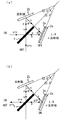
また、直交する方向に光の入出端が設けられる構成の2×2光切替スイッチの例として図25に示す構成がある。
図25(a)において、2×2光切替スイッチは、偏光ビームスプリッタ101に対して直交する2つの各側に、液晶セル103と反射板105とを組み合わせた光学素子、及び液晶セル104と反射板106とを組み合わせた光学素子を配置し、偏光ビームスプリッタ101を挟んで液晶セル103と対向する側にコリメータ107を介して光ファイバ109を接続し、偏光ビームスプリッタ101を挟んで液晶セル105と対向する側にコリメータ108を介して光ファイバ1010を接続する。この光ファイバ109,110は入射と出射とを兼ねているため、光ファイバ109,110にサーキュレータ111,112を接続することによって入射光と出射光を分離している。液晶セル103,104は、電圧の印加によって、入射した光の偏光状態をλ/4波長変化させる。この構成では、反射板と組み合わせることで、入射と出射で合わせて偏光状態がλ/2波長変化することになる。
【0005】
この構成による2×2光切替スイッチでは、スイッチ動作として入射端と出射端を異なる側とする状態(Exchanging state)と入射端と出射端を同じ側とする状態(Straight state)の二つの動作をとることができる。なお、偏光ビームスプリッタ101は、偏光分離合成膜102を備えている。
図25(b)はExchanging stateを説明するための図である。この動作状態では、液晶セル103及び液晶セル104に電圧を印加しない。光ファイバ109から入射した光は偏光面が直交する2つの偏光成分pと偏光成分sから成り、コリメータ107で平行ビームとなった後、偏光ビームスプリッタ101に入って偏光分離合成膜102により直進する偏光成分pと反射する偏光成分sに分離される。
【0006】
液晶セル103及び液晶セル104に電圧が印加されていない場合には、液晶セル103及び液晶セル104により偏光状態の変換が行われる。なお、図25(b)では、偏光状態の変換が行われる状態をONで表している。直進する偏光成分pは、λ/4波長だけ偏光状態が変化して液晶セル103を通過した後、反射板105で反射し再び液晶セル103を通過する。このとき、さらに偏光状態はλ/4波長変化し入射した偏光成分pは偏光成分sに変換される。変換された偏光成分sは、偏光分離合成膜102で反射され、コリメータ108を介して光ファイバ110に出射される。一方、偏光分離合成膜102で反射した偏光成分sは、λ/4波長だけ偏光状態が変化して液晶セル104を通過した後、反射板106で反射し再び液晶セル104を通過する。このとき、さらに偏光状態はλ/4波長変化し入射した偏光成分sは偏光成分pに変換される。変換された偏光成分pは、偏光分離合成膜102を通過し、コリメータ109を介して光ファイバ110に出射される。これによって、入射した光は入射端とは異なる端部から出射することになる。
【0007】
また、図25(c)はStraight stateを説明するための図である。この動作状態では、液晶セル103及び液晶セル104に電圧を印加する。液晶セル103及び液晶セル104に電圧が印加されている場合には、液晶セル103及び液晶セル104により偏光状態の変換が行われない。なお、図25(c)では、偏光状態の変換が行われない状態をOFFで表している。
【0008】
直進する偏光成分pは、λ/4波長だけそのままの偏光状態で液晶セル103を通過した後、反射板105で反射し再びそのままの偏光状態で液晶セル103を通過する。反射後、液晶セル103を通過した偏光成分pは、偏光分離合成膜102を直進し、コリメータ107を介して光ファイバ109に出射される。一方、偏光分離合成膜102で反射した偏光成分sは、そのままの偏光状態で液晶セル104を通過した後、反射板106で反射し再びそのままの偏光状態で液晶セル104を通過する。反射後、液晶セル104を通過した偏光成分sは、偏光分離合成膜102で反射し、コリメータ107を介して光ファイバ109に出射される。これによって、入射した光は入射端と同じ端部から出射することになる。
【0009】
なお、上記2×2光切替スイッチの構成及び2×2光切替スイッチを用いたアドドロップマルチプレクサの構成は、例えば、Optical Engineering,Vol.40 No.8, 1521-1528,August 2001 (Sarun Sumriddetchakajorn, Nabeel A.Riza, Deepak K.Sengupta)
に記載されている。
【0010】
【発明が解決しようとする課題】
光スイッチでは、入射と出射の入れ替えに対して機能が対称であることが求められる。上記した2×2光切替スイッチの構成では、入射と出射とを入れ替えた場合、光スイッチ内において偏光成分によって光路や通過する液晶セルや光学系が異なるため、必ずしも機能が対称とならない。入射と出射の入れ替えに対して機能を対称するには、光路長を合わせたり、液晶セルや光学系の特性を調整する必要があるという問題がある。この点は、構成に要する部品点数が多ければそれだけ調整箇所が増えるため、より大きな問題となり、また、製造コストにも影響することになる。
【0011】
また、光信号に生じる損失として偏波依存性損失(PDL:Polarization Dependent Loss)や偏波モード分散(PMD:Polarization Mode Dispesion)が知られている。偏波依存性損失は、例えば、液晶セルが備える電極の透過に伴う信号強度の低下によるものがあり、液晶セルを通過する回数が多い構成ではこの偏波依存性損失が大きくなるという問題がある。また、偏波モード分散は、直交する偏波モードによって光パルスの分散の程度が異なるため、光路長が異なればこの光分散による信号劣化が大きくなるという問題がある。
【0012】
また、液晶セルによって偏光状態を切り替える構成では、切替速度はこの液晶セルの切替速度に依存する。この液晶セルの切替速度は液晶セルの厚みの2乗に比例する特性があるため薄い液晶セルが求められるが、液晶セルの厚みは変換する偏光角度と光の波長によって定まるため、高速動作化が難しいという問題もある。
【0013】
そこで、本発明は、従来の課題を解決して、異なる経路を通る偏光に対して光路長や光学特性を同一とすることで、光路長や光学特性の調整を不要とし、また、偏波モード分散による信号劣化を低減することを目的とし、液晶セルの電極を通過する回数を低減することで偏波依存性損失を低減し、部品点数や調整箇所を低減あるいは削減する構成としてコストを低減すること目的とし、また、液晶セルの応答を速めて光スイッチを高動作化することを目的とする。
【0014】
【課題を解決するための手段】
本発明の光スイッチは、偏光分離合成手段と、少なくとも2つの反射手段と、偏光方向を制御する偏光制御手段とを備えた構成とし、偏光分離合成手段で分離された二つの偏光成分が同一光路を互いに進行方向を異にして偏光分離合成手段に再入射され合成されるように、偏光分離合成手段及び反射手段を配置すると共に、この光路上に偏光制御手段を配置し、偏光制御手段により各偏光成分の偏光方向を制御する。
【0015】
ここで、光路上に配置される偏光制御手段は、この光路上において全体でλ/2波長の偏光制御を行う。また、反射手段及び偏光分離合成手段が形成する光路は多角形を形成し、この多角形は、偏光分離合成手段における内角を直角とし、反射手段の個数から1を引いた個数に180度を乗じた角度を多角形の内角の和とするよう配置する。
【0016】
本発明の光スイッチによれば、偏光分離合成手段と少なくとも2つの反射手段、及び偏光制御手段の配置構成により、偏光分離合成手段で分離された二つの偏光成分は、同一光路をそれぞれ進行方向を異にして進み、偏光分離合成手段に再入射して合成される。また、二つの偏光成分は、同一光路上で同一の偏光制御手段を通過する。これによって、異なる経路であっても同一光路を通るため、光路長及び通過する光路上の光学特性が同一となる。従って、光路長や光学特性の調整が不要となり、偏波モード分散による信号劣化も低減することができる。
【0017】
また、従来の構成では、偏光成分に応じて異なる経路毎に偏光分離合成手段を設ける必要があるが、本発明の光スイッチによれば、同一光路上に配置した一つの偏光制御手段によって偏光状態を変換する構成であるため、偏光成分が偏光制御手段を通過する回数が低減されるため、偏波依存性損失を低減することができる。また、同一光路上に配置した一つの偏光制御手段を用いるため、部品点数や調整箇所を低減あるいは削減し、延いてはコストを低減することができる。
【0018】
また、液晶セルにより偏光制御手段を構成する場合には、液晶セルを反射手段に設ける等の光路上に配置する液晶セルの個数を増加させる構成とすることによって、各液晶セルの厚みを薄くすることができ、光スイッチの動作速度を高めることができる。
【0019】
本発明の光スイッチは、二つの偏光成分が同一光路を互いに進行方向を異にして偏光分離合成手段に再入射し、光路上に偏光制御手段を配置する構成として種々の態様とすることができる。
反射手段の配置の一態様において、反射手段は偏光分離合成手段に対して対称な位置において、2つの反射板を偏光成分の入射角及び出射角が22.5度となるように配置する。これによって、異なる経路であっても同一経路が形成される。
【0020】
この反射板の配置構成において、偏光制御手段の一配置態様は、λ/4波長の偏光制御を行う偏光制御手段を、二つの反射板の内の一方の反射板の光路上の前方位置に配置する。また、偏光制御手段の一配置態様は、λ/8波長の偏光制御を行う偏光制御手段を反射手段の両反射板の光路上の前方位置に配置する。
この偏光制御手段の配置により、異なる経路であっても同一経路を通ることで、何れの偏光成分についても同一の偏光制御を行うことができる。
【0021】
また、反射手段の配置の他の態様において、反射手段は偏光分離合成手段に対して対称な位置において、2つの反射板を偏光成分の入射角及び出射角を45度に配置し、さらに、1つの反射板を2つの反射板を結ぶ光路上であってこれらの反射板に対して垂直方向に配置する。
【0022】
この反射板の配置構成において、偏光制御手段の配置態様は、λ/4波長の偏光制御を行う偏光制御手段を、垂直方向に配置した1つの反射板や平行配置される2つの反射板等の光路上の反射板の前方位置に配置する。また、偏光制御手段の他の配置態様は、λ/12波長の偏光制御を行う偏光制御手段を、3つの各反射板の光路上の前方位置に配置する。
【0023】
また、反射手段及び偏光制御手段の配置の別の態様において、反射手段は偏光分離合成手段に対して対称な位置において、2つの反射板を偏光成分の入射角及び出射角を22.5度に配置し、λ/2波長の偏光制御を行う偏光制御手段を2つの反射板間の光路上に配置する。反射手段及び偏光制御手段の配置のさらに別の態様において、反射手段は偏光分離合成手段に対して対称な位置において、2つの反射板を偏光成分の入射角及び出射角を22.5度に配置し、λ/10波長の偏光制御を行う偏光制御手段を、2つの偏光制御手段の光路上の前方位置、及び2つの反射板間の光路上に配置する。
【0024】
これらの各反射手段及び偏光制御手段の配置により、異なる経路であっても同一経路を通ることで、何れの偏光成分についても同一の偏光制御を行うことができる。
また、本発明の光スイッチにおいて、偏光制御手段は、液晶セルで構成することができる。液晶セルは、偏光する角度により、s偏光とp偏光の偏光状態を90度変換して、偏光分離合成手段における通過と反射を制御するスイッチング用液晶セルとして用いる他、液晶や光路上に配置した偏光板に残留する残留複屈折によって生じる経路による偏光状態のずれを補償する残留複屈折補償用液晶セルとして用いることができる。残留複屈折の補償は、スイッチング用液晶セルと残留複屈折補償用液晶セルのダイレクタ方向を直交させ、両液晶セルの複屈折量が打ち消されるように電圧を印加する他、光路上に複屈折結晶あるいは異方性フィルムを配置することで行うことができる。
【0025】
また、液晶セルは、種々の構成とすることができる。一つの構成では、液晶セルに反射板を設けることにより反射手段を構成することができる。
この反射板を備える液晶セル構成において、一態様では、液晶セルの内部に反射板を配置する構成とすることができ、この構成において、液晶セルが備える二つの電極の一方の電極を反射板とすることができる。他の態様では、液晶セルの外部に反射板を配置する構成とすることができる。
【0026】
また、本発明の光スイッチにより2入力2出力スイッチを構成する態様として、一態様では、本発明の光スイッチの光路の両端に光軸を合わせて入出力ポートを配置し、この入出力ポートにサーキュレータを接続する構成とする。
また、他の態様では、本発明の光スイッチの光路の両端において、光路の光学的な中心に対して対称に、かつ光軸を合わせてそれぞれ2つの入出力ポートを配置する。この構成によれば、本発明の光スイッチはサーキュレータを要すること無く2入力2出力スイッチを構成することができ、また、本発明の光スイッチによってサーキュレータを構成こともできる。
また、本発明の光スイッチは、Add/Drop装置の構成要素としても用いることができ、また、偏光状態を制御することで、前記したスイッチングや残留複屈折補償の他、温度補償や減衰器として用いることもできる。
【0027】
【発明の実施の形態】
以下、本発明の実施の形態を図を参照しながら詳細に説明する。
図1は本発明の光スイッチの基本構成を説明するための概略図である。図1において、本発明の光スイッチは、偏光分離合成手段1と、少なくとも2つの反射手段2と、偏光方向を制御する偏光制御手段3とを備える。偏光分離合成手段1は、入射した光に含まれるp偏光成分とs偏光成分とに分離し、p偏光成分についてはそのまま直進させ、s偏光成分については反射させる。
【0028】
反射手段2(2A,2B)は、偏光分離合成手段1で分離された二つの偏光成分が同一光路を互いに進行方向を異にして偏光分離合成手段1に再入射するように配置する。図中に示すAで示される3角形は、偏光分離合成手段1及び反射手段2,3によって形成される光路を示し、図中のaで示す方向から入射した光についてみると、偏光分離合成手段1を直進し、反射手段2A及び反射手段2Bの順で反射された後、再び偏光分離合成手段1に戻る経路cと、偏光分離合成手段1で反射し、反射手段2B及び反射手段2Aの順で反射された後、再び偏光分離合成手段1に戻る経路dとが形成され、2つの経路c,dは同一の光路となる。なお、図中のbで示す方向から入射した光についてみても、偏光分離合成手段1,反射手段2A,2Bの配置は光学的に対称となるため、同様に2つの経路c,dは同一の光路となる。
【0029】
また、この光路上に偏光状態を制御する偏光制御手段3を配置する。なお、偏光制御手段3の配置位置は、光路上において種々の態様とすることができる。 この構成により、異なる経路であっても、同一光路長を有し、光路上において通過する反射手段や偏光制御手段等の光学素子も同一とすることができる。
なお、偏光分離合成手段1は偏光分離合成膜により形成することができ、また、偏光制御手段は液晶セルで形成することができる。
【0030】
次に、本発明の光スイッチの基本構成に基づく構成例、及びその構成例における動作状態について、図2,3、6〜10を用いて説明する。
第1の構成例を図2を用いて説明する。第1の構成例は、偏光分離合成手段1に対して対称な位置において、二つの反射板2A,2Bを偏光成分の入射角及び出射角が22.5度となるように配置する。なお、入射角及び出射角は図中においてθで示している。この構成例では、λ/4波長の偏光制御を行う偏光制御手段3aを2つの反射板2a,2bの内の一方の反射板(図では反射板2aの例を示しいるが、反射板2bとすることもできる)の光路上の前方位置に配置する。
【0031】
図2(a)は前記したExchanging stateに対応する動作を説明するための図である。この動作状態では、偏光制御手段による偏光変換を行わない。偏光制御手段として液晶セルを用いる場合には、液晶セルに電圧を印加することでこの動作状態とすることができる。図ではこの動作状態をOFFで示している。
入射端(図中のIN)から入射した光は偏光面が直交する2つの偏光成分pと偏光成分sから成り、図示しないコリメータで平行ビームとなった後、偏光分離合成手段1により直進する偏光成分pと反射する偏光成分sに分離される。
【0032】
この動作状態では偏光制御手段3aは偏光変換を行わないため、直進する偏光成分pは、そのままの偏光状態で偏光制御手段3aを通過した後、反射板2aで反射されて再び偏光制御手段3aを通過する。このとき、偏光状態は変化せずに偏光成分pのままである。偏光成分pは、さらに反射板2bで反射され、再び偏光分離合成手段1に達する。このときの偏光成分pの進行方向は、入射方向と直交する方向となる。この偏光成分pは偏光分離合成手段1を直進し、図示しないコリメータを介して図中でOUTで示される出射端から出射される。
【0033】
一方、偏光分離合成手段1で反射した偏光成分sは反射板2bで反射され、そのままの偏光状態で偏光制御手段3aを通過した後、反射板2aで反射されて再び偏光制御手段3aを通過する。このとき、偏光状態は変化せずに偏光成分sのままである。偏光成分sは再び偏光分離合成手段1に達し反射される。このときの反射方向は、入射方向と直交する方向となり、図示しないコリメータを介して図中でOUTで示される出射端から出射される。これによって、入射した光は入射端とは異なる端部から出射することになる。
【0034】
図2(b)は前記したStraight stateに対応する動作を説明するための図である。この動作状態では、偏光制御手段による偏光変換を行う。偏光制御手段として液晶セルを用いる場合には、液晶セルに電圧を印加しないことで動作状態とすることができる。図ではこの動作状態をONで示している。
入射端(図中のIN)から入射した光は図示しないコリメータで平行ビームとなった後、偏光分離合成手段1により直進する偏光成分pと反射する偏光成分sに分離される。
【0035】
この動作状態では偏光制御手段3aは偏光変換を行うため、直進する偏光成分pは偏光制御手段3aを通過することでλ/4波長変換された後反射板2aで反射し、再び偏光制御手段3aを通過することでλ/4波長変換されて偏光成分sに変換される。偏光成分sは、さらに反射板2bで反射し、再び偏光分離合成手段1に達する。このときの偏光成分sの進行方向は、入射方向と直交する方向となる。この偏光成分sは偏光分離合成手段1で反射され、図示しないコリメータを介して入射端と同じ出射端OUTから出射される。
【0036】
一方、偏光分離合成手段1で反射した偏光成分sは反射板2bで反射され、次に偏光制御手段3aを通過することでλ/4波長変換された後反射板2aで反射し、再び偏光制御手段3aを通過することでλ/4波長変換されて偏光成分pに変換される。偏光成分pは再び偏光分離合成手段1に達し直進する。このときの進行方向は、入射方向と逆方向となり、図示しないコリメータを介して入射端と同じ出射端OUTから出射される。これによって、入射した光は入射端とは同じ端部から出射することになる。
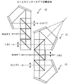
【0037】
第2の構成例を図3を用いて説明する。第2の構成例は、偏光分離合成手段1に対して対称な位置において、二つの反射板2a,2bを偏光成分の入射角及び出射角が22.5度となるように配置する。なお、入射角及び出射角は図中においてθで示している。この構成例では、λ/4波長の偏光制御を行う偏光制御手段3b,3cを2つの反射板2a,2bの光路上の前方位置に配置する。
【0038】
図3(a)は前記したExchanging stateに対応する動作を説明するための図である。この動作状態では、偏光制御手段による偏光変換を行わない。偏光制御手段として液晶セルを用いる場合には、液晶セルに電圧を印加することでこの動作状態とすることができる。図ではこの動作状態をOFFで示している。
入射端(図中のIN)から入射した光は図示しないコリメータで平行ビームとされて後、偏光分離合成手段1により直進する偏光成分pと反射する偏光成分sに分離される。
【0039】
この動作状態では偏光制御手段3bは偏光変換を行わないため、直進する偏光成分pは、そのままの偏光状態で偏光制御手段3bを通過した後、反射板2aで反射されて再び偏光制御手段3bを通過する。このとき、偏光状態は変化せずに偏光成分pのままである。偏光成分pは、さらに反射板2bで反射されると共に偏光制御手段3cを2回通過するが、偏光制御手段3cは偏光変換を行わないため偏光成分pのままである。反射板2bで反射された偏光成分pは再び偏光分離合成手段1に達する。このときの偏光成分pの進行方向は、入射方向と直交する方向となる。この偏光成分pは偏光分離合成手段1を直進し、図示しないコリメータを介して図中でOUTで示される出射端から出射される。
【0040】
一方、偏光分離合成手段1で反射した偏光成分sは、この動作状態では偏光制御手段3cは偏光変換を行わないため、そのままの偏光状態で偏光制御手段3cを通過した後、反射板2bで反射されて再び偏光制御手段3cを通過する。このとき、偏光状態は変化せずに偏光成分sのままである。偏光成分sは、さらに反射板2aで反射されると共に偏光制御手段3bを2回通過するが、偏光制御手段3bは偏光変換を行わないため偏光成分sのままである。反射板2aで反射された偏光成分sは再び偏光分離合成手段1に達し反射され、図示しないコリメータを介して図中でOUTで示される出射端から出射される。これによって、入射した光は入射端とは異なる端部から出射することになる。
【0041】
図3(b)は前記したStraight stateに対応する動作を説明するための図である。この動作状態では、偏光制御手段による偏光変換を行う。偏光制御手段として液晶セルを用いる場合には、液晶セルに電圧を印加しないことで動作状態とすることができる。図ではこの動作状態をONで示している。
入射端(図中のIN)から入射した光は図示しないコリメータで平行ビームとなった後、偏光分離合成手段1により直進する偏光成分pと反射する偏光成分sに分離される。
【0042】
この動作状態では偏光制御手段3bは偏光変換を行うため、直進する偏光成分pは偏光制御手段3bを通過することでλ/8波長変換された後反射板2aで反射し、再び偏光制御手段3bを通過することでλ/8波長変換されて、λ/4波長変換される。λ/4波長変換された偏光成分は、さらに反射板2bに反射において、偏光制御手段3cを2回通過する間にλ/8の変換を2回受けてλ/4波長変換される。これによって、偏光成分pは偏光成分sに変換される。変換された偏光成分sは、再び偏光分離合成手段1に達する。この偏光成分sは偏光分離合成手段1で反射され、図示しないコリメータを介して入射端と同じ出射端OUTから出射される。
【0043】
一方、偏光分離合成手段1で反射した偏光成分sは、反射板2bで反射される間に偏光制御手段3cを2回通過することでλ/4波長の変換を受け、さらに、反射板2aで反射される間に偏光制御手段3bを2回通過することでλ/4波長の変換を受けて偏光成分pに変換される。偏光成分pは再び偏光分離合成手段1に達し直進する。このときの進行方向は、入射方向と逆方向となり、図示しないコリメータを介して入射端と同じ出射端OUTから出射される。これによって、入射した光は入射端とは同じ端部から出射することになる。
【0044】
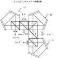
前記した第1,2の構成例は、図4に示す構成によって偏光分離合成手段、反射板、及び偏光制御手段の配置を行うことができる。
図4(a)は配置構成の一例である。この配置構成では、偏光分離合成膜10をプリズム11a,11bで挟むことによって偏光分離合成手段1を構成し、図示しないフレームに固定する。一方、反射板2a,2bについても、図示しないフレームに固定部材を設置し、この固定部材により位置決めを行う。偏光分離合成手段及び反射板の角度関係は、フレームに設けた固定部材により定めることができる。なお、この構成例では、反射板間は空気環境となる。
【0045】
図4(b)は配置構成の他の例である。この配置構成では、偏光分離合成膜10をプリズム11a,11bで挟むことによって偏光分離合成手段1を構成すると共に、反射板2a,2bについても台形のプリズム11cを挟む構成とし、プリズム11a,11bとプリズム11cとを接合して構成する。
この構成によれば、偏光分離合成手段及び反射板の角度関係は、プリズムにより設定することができ、さらに、光路はすべてプリズム内で形成することができるため、空気中を伝わる際に減衰や散乱を減少させることができる。
【0046】
第3の構成例を図5を用いて説明する。第3の構成例は、偏光分離合成手段に対して対称な位置において、2つの反射板2a,2bを偏光成分の入射角及び出射角を45度に配置し、さらに、1つの反射板2cを2つの反射板2a,2bを結ぶ光路上であってこれらの反射板2a,2bに対して垂直方向に配置する。 なお、入射角及び出射角は図中においてθで示している。この構成例では、λ/4波長の偏光制御を行う偏光制御手段3dを反射板2cの光路上の前方位置に配置する。
【0047】
図5(a)は前記したExchanging stateに対応する動作を説明するための図である。この動作状態では、偏光制御手段による偏光変換を行わない。偏光制御手段として液晶セルを用いる場合には、液晶セルに電圧を印加することでこの動作状態とすることができる。図ではこの動作状態をOFFで示している。
入射端(図中のIN)から入射した光は図示しないコリメータで平行ビームとされて後、偏光分離合成手段1により直進する偏光成分pと反射する偏光成分sに分離される。
【0048】
この動作状態では偏光制御手段3dは偏光変換を行わないため、直進する偏光成分pは、反射板2aで反射された後、そのままの偏光状態で偏光制御手段3dを通過した後、反射板2cで反射されて再び偏光制御手段3dを通過する。このとき、偏光状態は変化せずに偏光成分pのままである。偏光成分pは、さらに反射板2bで反射され、再び偏光分離合成手段1に達する。このときの偏光成分pの進行方向は、入射方向と直交する方向となる。この偏光成分pは偏光分離合成手段1を直進し、図示しないコリメータを介して図中でOUTで示される出射端から出射される。
【0049】
一方、偏光分離合成手段1で反射した偏光成分sは、この動作状態では偏光制御手段3dは偏光変換を行わないため、偏光成分sは、反射板2bで反射された後、そのままの偏光状態で偏光制御手段3dを通過した後、反射板2cで反射されて再び偏光制御手段3dを通過する。このとき、偏光状態は変化せずに偏光成分sのままである。偏光成分sは、さらに反射板2aで反射され、再び偏光分離合成手段1に達して反射され、図示しないコリメータを介して図中でOUTで示される出射端から出射される。これによって、入射した光は入射端とは異なる端部から出射することになる。
【0050】
図5(b)は前記したStraight stateに対応する動作を説明するための図である。この動作状態では、偏光制御手段による偏光変換を行う。偏光制御手段として液晶セルを用いる場合には、液晶セルに電圧を印加しないことで動作状態とすることができる。図ではこの動作状態をONで示している。
入射端(図中のIN)から入射した光は図示しないコリメータで平行ビームとなった後、偏光分離合成手段1により直進する偏光成分pと反射する偏光成分sに分離される。
【0051】
この動作状態では偏光制御手段3dは偏光変換を行うため、直進する偏光成分pは、反射板2aで反射された後、偏光制御手段3dを通過することでλ/4波長変換された後反射板2cで反射し、再び偏光制御手段3dを通過することでλ/4波長変換されて、偏光成分sに変換される。偏光成分sは反射板2bで反射されて再び偏光分離合成手段1に達する。この偏光成分sは偏光分離合成手段1で反射され、図示しないコリメータを介して入射端と同じ出射端OUTから出射される。
【0052】
一方、偏光分離合成手段1で反射した偏光成分sは、反射板2bで反射された後、偏光制御手段3dを通過することでλ/4波長変換された後反射板2cで反射し、再び偏光制御手段3dを通過することでλ/4波長変換されて、偏光成分pに変換される。変換された偏光成分pは反射板2aで反射されて再び偏光分離合成手段1に達する。この偏光成分pは偏光分離合成手段1を直進し、図示しないコリメータを介して入射端と同じ出射端OUTから出射される。これによって、入射した光は入射端とは同じ端部から出射することになる。
なお、第4の構成例において、偏光制御手段3dの配置位置は上記構成例に示す反射板2cに位置に限らず、反射板2aあるいは反射板2b等の任意の位置とすることができる。
【0053】
第4の構成例を図6を用いて説明する。第4の構成例は、偏光分離合成手段に対して対称な位置において、2つの反射板を偏光成分の入射角及び出射角を45度に配置し、さらに、1つの反射板を2つの反射板を結ぶ光路上であってこれらの反射板に対して垂直方向に配置する。偏光制御手段の他の配置態様は、λ/12波長の偏光制御を行う偏光制御手段を、3つの各反射板の光路上の前方位置に配置する。
なお、入射角及び出射角は図中においてθで示している。この構成例では、λ/12波長の偏光制御を行う偏光制御手段3e,3f,3gを各反射板2a,2b,2cに配置する。
【0054】
図6(a)は前記したExchanging stateに対応する動作を説明するための図である。この動作状態では、偏光制御手段による偏光変換を行わない。偏光制御手段として液晶セルを用いる場合には、液晶セルに電圧を印加することでこの動作状態とすることができる。図ではこの動作状態をOFFで示している。
入射端(図中のIN)から入射した光は図示しないコリメータで平行ビームとされて後、偏光分離合成手段1により直進する偏光成分pと反射する偏光成分sに分離される。
【0055】
この動作状態では偏光制御手段3e,3f,3gは偏光変換を行わないため、直進する偏光成分pは、各反射板2a,2b,2cで反射されて偏光分離合成手段1に戻る。偏光成分pは、この各反射板2a,2b,2cに設けた偏光制御手段3e,3f,3gを通過する際に偏光変換されないため、そのままの偏光状態で偏光分離合成手段1に戻る。このときの偏光成分pの進行方向は、入射方向と直交する方向となる。この偏光成分pは偏光分離合成手段1を直進し、図示しないコリメータを介して図中でOUTで示される出射端から出射される。
【0056】
一方、偏光分離合成手段1で反射した偏光成分sは、この動作状態では偏光制御手段3e,3f,3gは偏光変換を行わないため、反射された偏光成分sは、各反射板2a,2b,2cで反射されて偏光分離合成手段1に戻る。偏光成分sは、この各反射板2a,2b,2cに設けた偏光制御手段3e,3f,3gを通過する際に偏光変換されないため、そのままの偏光状態で偏光分離合成手段1に戻って反射され、図示しないコリメータを介して図中でOUTで示される出射端から出射される。
これによって、入射した光は入射端とは異なる端部から出射することになる。
【0057】
図6(b)は前記したStraight stateに対応する動作を説明するための図である。この動作状態では、偏光制御手段による偏光変換を行う。偏光制御手段として液晶セルを用いる場合には、液晶セルに電圧を印加しないことで動作状態とすることができる。図ではこの動作状態をONで示している。
入射端(図中のIN)から入射した光は図示しないコリメータで平行ビームとなった後、偏光分離合成手段1により直進する偏光成分pと反射する偏光成分sに分離される。
【0058】
この動作状態では偏光制御手段3e,3f,3gは偏光変換を行うため、直進する偏光成分pは、各反射板で反射されるたびにλ/12波長の偏光変換を2回受けてλ/6波長の偏光変換が行われる。このλ/6波長の偏光変換を3つの反射板2a,2b,2cで行うことにより、λ/2波長の偏光変換を受けて偏光成分sに変換される。偏光成分sは反射板2bで反射されて再び偏光分離合成手段1に達する。この偏光成分sは偏光分離合成手段1で反射され、図示しないコリメータを介して入射端と同じ出射端OUTから出射される。
【0059】
一方、偏光分離合成手段1で反射した偏光成分sは、偏光成分pと同様に、逆の経路を通って各反射板で反射されるたびにλ/12波長の偏光変換を2回受けてλ/6波長の偏光変換が行われる。このλ/6波長の偏光変換を3つの反射板2a,2b,2cで行うことにより、λ/2波長の偏光変換を受けて偏光成分pに変換される。変換された偏光成分pは反射板2aで反射されて再び偏光分離合成手段1に達する。この偏光成分pは偏光分離合成手段1を直進し、図示しないコリメータを介して入射端と同じ出射端OUTから出射される。これによって、入射した光は入射端とは同じ端部から出射することになる。
【0060】
第5の構成例を図7を用いて説明する。第5の構成例は、第3,4の構成例と同様に、3つの反射板を互いに直交に配置する構成であり、偏光分離合成手段1と隣接する何れか一方の反射板をプリズム等の全反射ミラーとし、残りの2つの反射板の光路上の前方位置にλ/8波長の偏光制御を行う偏光制御手段を配置する。
図7では、反射板2bをプリズムとし、反射板2a,2cの光路上の前方位置にλ/8波長2b偏光制御を行う偏光制御手段を配置する構成を示している。なお、図7では偏光制御手段を省略して示している。
【0061】
第6の構成例を図8を用いて説明する。第6の構成例は、偏光分離合成手段に対して対称な位置において、2つの反射板を偏光成分の入射角及び出射角を22.5度に配置し、λ/2波長の偏光制御を行う偏光制御手段を2つの反射板間の光路上に配置する。なお、入射角及び出射角は図中においてθで示している。この構成例では、λ/2波長の偏光制御を行う偏光制御手段3hを反射板2a,2bの間の光路上に配置する。
【0062】
図8(a)は前記したExchanging stateに対応する動作を説明するための図である。この動作状態では、偏光制御手段による偏光変換を行わない。偏光制御手段として液晶セルを用いる場合には、液晶セルに電圧を印加することでこの動作状態とすることができる。図ではこの動作状態をOFFで示している。
入射端(図中のIN)から入射した光は図示しないコリメータで平行ビームとされて後、偏光分離合成手段1により直進する偏光成分pと反射する偏光成分sに分離される。
【0063】
この動作状態では偏光制御手段3hは偏光変換を行わないため、直進する偏光成分pは、反射板2aで反射された後、そのままの状態で偏光制御手段3hを通り、反射板2bで反射されて偏光分離合成手段1に戻る。このときの偏光成分pの進行方向は、入射方向と直交する方向となる。この偏光成分pは偏光分離合成手段1を直進し、図示しないコリメータを介して図中でOUTで示される出射端から出射される。
【0064】
一方、偏光分離合成手段1で反射した偏光成分sは、この動作状態では偏光制御手段3hは偏光変換を行わないため、反射された偏光成分sは、反射板2bで反射された後、そのままの状態で偏光制御手段3hを通り、反射板2aで反射されて偏光分離合成手段1に戻って反射され、図示しないコリメータを介して図中でOUTで示される出射端から出射される。これによって、入射した光は入射端とは異なる端部から出射することになる。
【0065】
図8(b)は前記したStraight stateに対応する動作を説明するための図である。この動作状態では、偏光制御手段による偏光変換を行う。偏光制御手段として液晶セルを用いる場合には、液晶セルに電圧を印加しないことで動作状態とすることができる。図ではこの動作状態をONで示している。
入射端(図中のIN)から入射した光は図示しないコリメータで平行ビームとなった後、偏光分離合成手段1により直進する偏光成分pと反射する偏光成分sに分離される。
【0066】
この動作状態では偏光制御手段3hは偏光変換を行うため、直進する偏光成分pは、反射板2aで反射された後、偏光制御手段3hを通る間に偏光成分sに変換され、反射板2bで反射されて偏光分離合成手段1に戻る。このときの偏光成分sの進行方向は入射方向と直交する方向となり、偏光分離合成手段1で反射され、図示しないコリメータを介して図示しないコリメータを介して入射端と同じ出射端OUTから出射される。
【0067】
一方、偏光分離合成手段1で反射した偏光成分sは、反射板2bで反射された後、偏光制御手段3hを通る間に偏光成分pに変換され、反射板2aで反射されて偏光分離合成手段1に戻る。このときの偏光成分pの進行方向は入射方向と逆方向となり、偏光分離合成手段1を直進し、図示しないコリメータを介して図示しないコリメータを介して入射端と同じ出射端OUTから出射される。これによって、入射した光は入射端と同じ端部から出射することになる。
【0068】
第7の構成例を図9を用いて説明する。第7の構成例は、偏光分離合成手段に対して対称な位置において、2つの反射板を偏光成分の入射角及び出射角を22.5度に配置し、λ/10波長の偏光制御を行う偏光制御手段を、2つの反射板の光路上の前方位置、及び2つの反射板間の光路上に配置する。なお、入射角及び出射角は図中においてθで示している。この構成例では、λ/10波長の偏光制御を行う偏光制御手段3i,3jを反射板2a,2bに配置し、λ/10波長の偏光制御を行う偏光制御手段3kを反射板2aと反射板2bとの間の光路上に配置する。
【0069】
図9(a)は前記したExchanging stateに対応する動作を説明するための図である。この動作状態では、偏光制御手段による偏光変換を行わない。偏光制御手段として液晶セルを用いる場合には、液晶セルに電圧を印加することでこの動作状態とすることができる。図ではこの動作状態をOFFで示している。
入射端(図中のIN)から入射した光は図示しないコリメータで平行ビームとされて後、偏光分離合成手段1により直進する偏光成分pと反射する偏光成分sに分離される。
【0070】
この動作状態では偏光制御手段3i,3j,3kは偏光変換を行わないため、直進する偏光成分pは、各反射板2a、2bで反射される経路上において、そのままの状態で偏光制御手段3i,3j,3kを通り、反射板2bで反射されて偏光分離合成手段1に戻る。このときの偏光成分pの進行方向は、入射方向と直交する方向となる。この偏光成分pは偏光分離合成手段1を直進し、図示しないコリメータを介して図中でOUTで示される出射端から出射される。
【0071】
一方、偏光分離合成手段1で反射した偏光成分sは、偏光制御手段3i,3j,3kは偏光変換を行わないため、反射された偏光成分sは、反射板2bで反射された後、そのままの状態で偏光制御手段3i,3j,3kを通り、反射板2aで反射されて偏光分離合成手段1に戻って反射され、図示しないコリメータを介して図中でOUTで示される出射端から出射される。これによって、入射した光は入射端とは異なる端部から出射することになる。
【0072】
図9(b)は前記したStraight stateに対応する動作を説明するための図である。この動作状態では、偏光制御手段による偏光変換を行う。偏光制御手段として液晶セルを用いる場合には、液晶セルに電圧を印加しないことで動作状態とすることができる。図ではこの動作状態をONで示している。
入射端(図中のIN)から入射した光は図示しないコリメータで平行ビームとなった後、偏光分離合成手段1により直進する偏光成分pと反射する偏光成分sに分離される。
【0073】
この動作状態では偏光制御手段3i,3j,3kは偏光変換を行うため、直進する偏光成分pは、反射板2aで反射される際に偏光制御手段3iによりλ/10波長の偏光変換を2回受けてλ/5波長の偏光変換され、偏光制御手段3kの通過によりλ/10波長の偏光変換され、さらに、反射板2aで反射される際に偏光制御手段3jによりλ/10波長の偏光変換を2回受けてλ/5波長の偏光変換され、最終的にλ/2波長の偏光変換により偏光成分sに偏光変換される。偏光成分sは、反射板2bで反射されて偏光分離合成手段1に戻る。このときの偏光成分sの進行方向は入射方向と直交する方向となり、偏光分離合成手段1で反射され、図示しないコリメータを介して図示しないコリメータを介して入射端と同じ出射端OUTから出射される。
【0074】
一方、偏光分離合成手段1で反射した偏光成分sは、反射板2bで反射される際に偏光制御手段3jによりλ/10波長の偏光変換を2回受けてλ/5波長の偏光変換され、偏光制御手段3kの通過によりλ/10波長の偏光変換され、さらに、反射板2aで反射される際に偏光制御手段3iによりλ/10波長の偏光変換を2回受けてλ/5波長の偏光変換され、最終的にλ/2波長の偏光変換により偏光成分pに偏光変換され、偏光分離合成手段1に戻る。偏光成分pは偏光分離合成手段1を直進し、図示しないコリメータを介して図示しないコリメータを介して入射端と同じ出射端OUTから出射される。これによって、入射した光は入射端と同じ端部から出射することになる。
【0075】
図10は、第1〜7の構成例を用いた2×2光スイッチの構成例である。図10において、本発明の光スイッチ100に対してコリメータ107,108を介して光ファイバ109,110を接続し、この光ファイバ109,110にサーキュレータ107,108を取り付けることにより、2×2光スイッチを構成することができる。ここで、サーキュレータ107,108は、同光ファイバを通る光信号の分離に用いられる。
【0076】
次に、本発明の光スイッチの基本構成に基づく他の構成例、及びその構成例における偏光状態を図11〜13を用いて説明する。
この構成例は、図1で示した光スイッチの基本構成において、入射端及び出射端において、2つの入出力ポートを光路の光学的な中心に対して対称に、かつ光軸を合わせて配置する。
【0077】
図11(a)において、2つの入出力ポート4a,4b、及び2つの入出力ポート5a,5bを備え、入出力ポート4a,4bは光路oの光学的な中心pに対して光軸を合わせて設定され、また、入出力ポート5a,5bについても光路oの光学的な中心pに対して光軸を合わせて設定される。この構成により、光スイッチにおいてサーキュレータを不要とすることができる。
【0078】
図11(b)は、光スイッチの動作を説明するものである。例えば、入出力ポート4bから入力した信号は、サーキュレータを要することなく入出力ポート5aあるいは入出力ポート4aから切り替えて出力することができ、また、入出力ポート5bから入力した信号は、サーキュレータを要することなく入出力ポート4aあるいは入出力ポート5aから切り替えて出力することができる。
【0079】
図12は、上記構成による動作を説明するために図である。図12(a)は、入出力ポート4aから入射した光を入出力ポート5bから出射する場合の動作である。この動作においては、図示しない偏光制御手段による偏光変換を行わない。入出力ポート4aから入射した光の偏光成分pと偏光成分sは、偏光分離合成手段1で分離された後、反射手段2A,2Bで反射されて入出力ポート5bに達する。このとき、各入出力ポートは、光路の光学的な中心に対して対称に、かつ光軸を合わせて配置されているため、前記図11(b)に示すように、交差した状態で他方の入出力ポート5bから出射される。
【0080】
一方、図12(b)は、入出力ポート4aから入射した光を同じ側の入出力ポート4bから出射する場合の動作である。この動作においては、図示しない偏光制御手段による偏光変換を行うことによって行う。入出力ポート4bから入射した光の偏光成分pと偏光成分sは、偏光分離合成手段1で分離された後、反射手段2A,2Bで反射されと共に光路上で偏光変換され、入出力ポート5bに達する。このとき、各入出力ポートは、光路の光学的な中心に対して対称に、かつ光軸を合わせて配置されているため、交差した状態で同じ側の入出力ポート4bから出射される。
この構成による光スイッチに光ファイバを接続するコリメータは、図13に示すように、2芯のコリメータを適用することができる。2芯のコリメータ6は、図11,12中の4a,4bあるいは5a,5bに対応して配置される。
【0081】
次に、本発明の光スイッチにおいて、片偏光を用いた光スイッチ構成例について図14〜図18を用いて説明する。
図14は、前記図7に示した構成において、片偏光のみを用いて光スイッチを構成する例であり、図14(a)は1×2光スイッチであり、図14(b)は2×2光スイッチである。
【0082】
図14(a)に示す1×2光スイッチは、本発明の光スイッチAが備える偏光分離合成手段1の一端に偏光分離合成手段1aを配置し、偏光分離合成手段1aの一端を入力端(IN)とし、偏光分離合成手段1aの他端及び偏光分離合成手段1の他端を出力端(それぞれ、OUT2,OUT1)とする。
この構成によれば、例えば入力端INから入力した場合には、光スイッチAによる偏光変換を行わない状態では出力端OUT1から出力し、光スイッチAによる偏光変換を行う状態では出力端OUT2から出力する。
【0083】
また、図14(b)に示す2×2光スイッチは、本発明の光スイッチAが備える偏光分離合成手段1の一端に偏光分離合成手段1aを配置し、他端に偏光分離合成手段1bを配置し、偏光分離合成手段1a,1bの一端を入力端(IN1,IN2)とし、偏光分離合成手段1a,1bの他端を出力端(それぞれ、OUT2,OUT1)とする。なお、図14(b)の構成例では、出力の偏光状態を合わせるために、入力端IN2と出力端OUT2にλ/2の波長板を配置している。
【0084】
この構成によれば、例えば入力端IN1に入力した場合には、光スイッチAによる偏光変換を行わない状態ではOUT1から出力し、光スイッチAによる偏光変換を行う状態ではOUT2から出力する。また、同様に、入力端IN2に入力した場合には、光スイッチAによる偏光変換を行わない状態ではOUT2から出力し、光スイッチAによる偏光変換を行う状態ではOUT1から出力する。
【0085】
また、図15は片偏光のみを用いた2×2光スイッチの別の構成例である。この構成例は、前記図4に示した構成において、光スイッチBが備える偏光分離合成手段1の一端に偏光分離合成手段1aを配置し、他端に偏光分離合成手段1bを配置し、偏光分離合成手段1a,1bの一端を入力端(IN1,IN2)とし、偏光分離合成手段1a,1bの他端を出力端(それぞれ、OUT2,OUT1)とする。なお、図15の構成例では、出力の偏光状態を合わせるために、入力端IN2と出力端OUT2にλ/2の波長板を配置している。
【0086】
この構成においても、例えば入力端IN1に入力した場合には、光スイッチBによる偏光変換を行わない状態ではOUT1から出力し、光スイッチAによる偏光変換を行う状態ではOUT2から出力する。また、同様に、入力端IN2に入力した場合には、光スイッチBによる偏光変換を行わない状態ではOUT2から出力し、光スイッチAによる偏光変換を行う状態ではOUT1から出力する。 この片偏光のみを用いた2×2光スイッチは、光切替の機能の他にアッテネータ(減衰器)としても用いることができる。
【0087】
図16〜図18は、2×2光スイッチとアッテネータとの組み合わせ構成例であり、図15に示した構成例を組み合わせることにより構成することができる。図16〜図18に示す2×2光スイッチとアッテネータとの組み合わせ構成は、それぞれ3つの光スイッチC1,C2,C3を組合わせ、この内の光スイッチC1を光切り替え手段として使用し、残りの光スイッチC2,C3をアッテネータとして使用する。
【0088】
アッテネータを構成する光スイッチC2,C3の端部の内、光スイッチC1と接続する側の端部には偏光分離合成手段が配置され、この端部に例えばマルチモードファイバ(MMF)を接続することにより、アッテネータで減衰された偏光成分を外部に排出することができる。アッテネータで減衰した偏光成分をMMFから外部に排出することにより、この構成ではアッテネータから熱源を除くことができ、冷却手段を設ける必要がないという効果がある。
【0089】
この構成によれば、例えば図16の構成では、例えば入力端IN1に入力した場合には、光スイッチAによる偏光変換を行わない状態ではOUT1から出力し、光スイッチAによる偏光変換を行う状態ではOUT2から出力する。また、同様に、入力端IN2に入力した場合には、光スイッチAによる偏光変換を行わない状態ではOUT2から出力し、光スイッチAによる偏光変換を行う状態ではOUT1から出力する。
【0090】
このとき、例えば、OUT1から出力する場合には、光スイッチC2によるアッテネータで減衰された偏光成分はMMF1から排出され、また、OUT2から出力する場合には、光スイッチC3によるアッテネータで減衰された偏光成分はMMF2から排出される。なお、図17、図18については同様であるため省略する。
【0091】
この構成によれば、図16〜図18に示すように、2×2光スイッチとアッテネータとの種々の配置で組み合わせることにより、入力端や出力端の配置位置を必要に応じた構成とすることができる。
さらに、この構成によれば、前記した二次元配置に限らず、三次元配置とすることもできる。図19(a),(b)は三次元配置による2×2光スイッチとアッテネータとの組み合わせの一構成例である。なお、図19(b)は図19(a)に示す構成におけるλ/2波長板の配置位置を示している。
【0092】
片偏光を用いた構成では配置によって偏光方向が変化するため、光スイッチとして適用させるために所定位置にλ/2波長板を配置する。図19に示す構成例は、入射直線偏光としてp偏光(片偏光)を用いた場合であり、この構成例では図19(b)に示す位置にλ/2波長板を配置することにより光スイッチを構成することができる。
【0093】
図19において、前記光スイッチC1,C2,C3に対応する光スイッチブロックD1,D2,D3を重ねて配置し、各光スイッチブロックD1,D2,D3に偏光分離合成ブロックE1,E2,E3,E4を隣接して配置することにより三次元で配置する。ここで、光スイッチブロックD1は光切り替え手段として使用し、残りの光スイッチブロックD2,D3がアッテネータとして使用する。
【0094】
この三次元配置の構成においても、前記二次元配置と同様に、入力端IN1に入力した場合には、偏光変換を行わない状態ではOUT1から出力し、偏光変換を行う状態ではOUT2から出力する。また、同様に、入力端IN2に入力した場合には、偏光変換を行わない状態ではOUT2から出力し、偏光変換を行う状態ではOUT1から出力する。また、光スイッチブロックD2,D3のアッテネータからは図示しないMMFを介して減衰による偏光成分を排出することができる。なお、図19(b)は、λ/2波長板を配置した構成例を示している。
【0095】
なお、図19では、光スイッチブロックD1,D2,D3を分けて示しているが、柱状の一つの偏光分離合成手段による構成することができる。
この三次元配置によれば、二次元配置と比較して部品点数を減らすことができる。また、各部材の入出力端の干渉を最小限とする構成をとることができ、装置構成の小型化を図ることができる。
【0096】
図20は、本発明の光スイッチに用いる偏光制御手段に適用することができる液晶セルの構成例である。
ここでは、液晶セルと反射板とを組み合わせた構成について説明する。液晶セルと反射板との組み合わせにおいて、光入射側から見たとき、反射板を液晶セルの外側に配置する構成と、反射板を液晶セルの内側に配置する構成がある。図20(a)は反射板を液晶セルの外側に配置する構成例を示し、図20(b),20(c)は反射板を液晶セルの内側に配置する構成例を示している。
【0097】
図20(a)において、液晶セル20は、光入射側から順に、ガラス等の基板21a、ITO等の透明電極膜22a、配向膜23a、液晶層24、配向膜23b、透明電極膜22b、基板21b、外部反射板25を配置して構成される。ここで、外部反射板25は、誘電体多層膜、アルミや金等の高反射性材料からなる金属膜とすることができる。
【0098】
また、図20(b)において、液晶セル20は、光入射側から順に、ガラス等の基板21a、ITO等の透明電極膜22a、配向膜23a、液晶層24、配向膜23b、内在反射板26、導電膜27、基板21bを配置して構成される。ここで、内在反射板26は、導電膜27による電場印加を行うために誘電体多層膜とする。また、導電膜27はITOによる透明電極膜を用いることができ、基板21bはガラス等の透明な材料に限らず不透明な材料を用いることもできる。
【0099】
また、図20(c)において、液晶セル20は、光入射側から順に、ガラス等の基板21a、ITO等の透明電極膜22a、配向膜23a、液晶層24、配向膜23b、内在反射板28、基板21bを配置して構成される。ここで、内在反射板28は、下部電極を兼ねるため金属膜とする。基板21bはガラス等の透明な材料に限らず不透明な材料を用いることもできる。
【0100】
上記各構成の液晶セルにおいて、配向膜の下部(あるいは電極の上部)に上下の基板の短絡防止用絶縁膜を形成することもできる。また、液晶セルとプリズムとの間に空気層が介在する構成では、液晶セルの表面において不要な反射を防止するために、誘電体多層膜による反射防止膜(AR:Antireflection Coating)を形成することが望ましい。
また、液晶素子の配向は、アンチパラレル配向又はパラレル配向とすることができる。また、液晶は強誘電体液晶やツイストネマチック液晶等を使用することができる。
【0101】
液晶セルにおいて、本発明の光スイッチは、入射直線偏光の方位角を90度回転と、そのままの状態による0度回転の2つの状態で制御するスイッチ動作を行うことができる。また、階調制御を行うことができる液晶を用いることで、中間状態の偏光によって可変光減衰器を構成することもできる。
また、本発明の光スイッチの複数の液晶セルを用いた構成において、偏光変換を行う液晶セルを選択することで、偏光成分sのみあるいは偏光成分pのみを取り出すことができ、これによって、可変光減衰器を構成することもできる。
【0102】
また、液晶セルのスイッチ動作を利用して光の切替を行う場合には、この液晶セルの応答速度は液晶セルの厚みに依存する。本発明の光スイッチでは、前記した第2,4,6の構成例に示すように、λ/2波長の偏光変換を行うために複数の液晶セルを用いる構成とすることで各液晶の厚みを薄くして応答速度を速めることができる。
【0103】
例えば、第2の構成例では、同一の反射型の液晶セルで比較したとき、各液晶セルの厚みは1/2となり、応答速度は2乗で反映されるため4倍となり、第4の構成例では、同様に、各液晶セルの厚みは1/3となって応答速度は9倍となり、第6の構成例では、同様に、各液晶セルの厚みは2/5となって応答速度は約6倍となる。
【0104】
また、本発明の光スイッチに用いる液晶セルは、その液晶セルの残留複屈折補償に用いることができる。以下、図21〜図23を用いて液晶セルによる光の残留複屈折補償について説明する。
図21(a)に示す本発明の光スイッチの基本構成において、光路は反射板に対して鏡面対称であるため、光路は図21(b)に示すように、等価的に光路に沿って展開して示すことができる。なお、a,bは液晶セルを示している。ここで、光は液晶セルに対して角度(図ではθ)を有して入射しているため、図21(b)に示すように、光路は液晶セルa,bの法線方向nに対してθの角度を有する。
【0105】
図22(a),(b)は、液晶セルaに対する入射光線ベクトルと、この入射光線ベクトルの液晶セルa表面への射影ベクトルmの関係を示している。なお、図22(b)は、法線方向n(図22(a)中の白抜きの矢印方向)から見た図である。ここで、射影ベクトルmと液晶セルのダイレクト方向とのなす角をφとすると、このときの液晶の残留複屈折(リターデーション)は、
Γ=(2πd/λ)・[ne・√(1−(sin2θ・sin2φ/ne2)−(sin2θ・cos2φ/no2))−√(1−(sin2θ/no2))]
で表される。なお、ここで、Γは残留複屈折、dはセルギャップ、neは異常光屈折率、noは常光屈折率である。上記した残留複屈折Γの式は、Pochi Yeh and Claire Gu.“Optics of Liquid Crystal Displays”, p.155,(1999),John Wiley £ Sons, Inc. を参照するものである。
【0106】
上記式において、垂直入射の場合にはθ=0であるので、
Γ=2π/λ・d(ne−no)
となる。
したがって、本発明のスイッチング用液晶セルにおいては、斜め入射条件でのΓが所定のλ/4(又は、所定のλ/8,λ/10など)の値となるようにセルギャップdを定める。
また、本発明の残留複屈折補償用液晶セルにおいては、図22(c)に示すように、スイッチング用液晶セルの液晶ダイレクタ方向と90度の関係とすることで残留複屈折を補償する。
【0107】
以下、本発明の残留複屈折補償用液晶セルによる残留複屈折補償について、図23の液晶セルの印加電圧と残留複屈折特性との概念図を用いて説明する。
図23に示す液晶セルの印加電圧と残留複屈折特性において、残留複屈折Γを0に近づけるには、液晶セルに通常百数十[V]以上の電圧が必要となる。
そこで、本発明では、スイッチング用液晶セルの液晶ダイレクタ方向と残留複屈折補償用液晶セルの液晶ダイレクタ方向とを直交するように設定する。なお、図22ではX−Z軸面内でp偏光が振動すると仮定している。
【0108】
以下、残留複屈折を補償する3つの方法について説明する。
第1の方法では、残留複屈折補償用液晶セルに常時電圧Vrを印加する。このとき残留複屈折補償用液晶セルの残留複屈折はΓ=Γrとなる。ここで、スイッチング用液晶セルに同じ電圧Vrを印加すると複屈折量はΓrとなり、2つの液晶セルのダイレクタ方向方向が直交しているため、複屈折は打ち消しあって残留複屈折は0となる。なお、このとき、スイッチング用液晶セル及び残留複屈折補償用液晶セルを反射した光はトータルで変調を受けないため、例えば入射p偏光はp偏光のままである。
【0109】
次に、スイッチング用液晶セルにのみ小電圧Voを印加すると、スイッチング用液晶セル及び残留複屈折補償用液晶セルの合成残留複屈折は
Γo−Γr=Γsw
となる。このΓswをλ/2とすれば、p偏光をs偏光に変換できるため、光路を変えることができる。
【0110】
第2の方法では、残留複屈折補償用液晶セルに常時Voを印加し、スイッチング用液晶セルにVoを印加することによりΓoをキャンセルする。また、スイッチング用液晶セルにVrを印加すると、二つの液晶セルを通過した後の合成残留複屈折は
Γo−Γr=Γsw
となる。このΓswをλ/2とすれば、p偏光をs偏光に変換できるため、光路を変えることができる。
【0111】
また、第3の方法では、残留複屈折補償用液晶セルを用いる代りに、光路上の任意の箇所に複屈折結晶あるいは異方性フィルムを配置し、これにより常時Γr(又はΓo)を形成して残留複屈折を補償する。光の切替はスイッチング用液晶セルによって行う。
【0112】
図24は、本発明の光スイッチに用いた、アド・ドロップ(Add/Drop)を含む構成例である。
図24に示す構成例は、サーキュレータ31,分波合成器32,本発明の光スイッチ33(SW1〜SWn),分波合成器34,及びサーキュレータ35を接続して構成する。図24(a)は、例えば、サーキュレータ31の分波合成器32に接続されない一端を入力端、他の一端をドロップ端とし、サーキュレータ35の分波合成器34に接続されない一端を入力端、他の一端をドロップ端としている。
【0113】
ここで、例えば、光スイッチSW1〜SWnをそれぞれλ1〜λnに対応させ、入力端からλ1〜λnに信号を入力した場合について説明する。入力端から入力したλ1〜λnの信号は分波合成器32で各波長に分波される。ここで、図24(b)に示すように、光スイッチ33のSW2のみを切り替えると、波長λ2の信号はサーキュレータ31のドロップ端から出力され、残りの波長λ1,λ3〜λnはサーキュレータ35のスルー端から出力される。また、このとき図24(c)に示すようにAND端からλ2を入力すると、入力した波長λ2の信号はサーキュレータ31のスルー端から出力される。
【0114】
なお、この構成例における、サーキュレータ,分波合成器,及び光スイッチの配置は、前記したOptical Engineering,Vol.40 No.8, 1521-1528,August 2001 (Sarun Sumriddetchakajorn, Nabeel A.Riza, Deepak K.Sengupta)に記載される構成例の配置と同様である。
また、本発明の光スイッチは、この他に光クロスコネクトの構成部品としても用いることができる。
【0115】
【発明の効果】
以上説明したように、本発明の光スイッチによれば、異なる経路を通る偏光に対して光路長や光学特性を同一とすることで、光路長や光学特性を調整を不要とすることができ、また、偏波モード分散による信号劣化を低減することができる。
【0116】
また、液晶セルの電極を通過する回数を低減することで偏波依存性損失を低減し、部品点数や調整箇所を低減あるいは削減する構成としてコストを低減することができる。
また、液晶セルの応答を速めて光スイッチを高動作化することができる。
【図面の簡単な説明】
【図1】本発明の光スイッチの基本構成を説明するための概略図である。
【図2】本発明の光スイッチの基本構成に基づく第1の構成例及び動作状態を説明するための図である。
【図3】本発明の光スイッチの基本構成に基づく第2の構成例及び動作状態を説明するための図である。
【図4】本発明の第1,2の構成例の配置を説明するための図である。
【図5】本発明の光スイッチの基本構成に基づく第3の構成例及び動作状態を説明するための図である。
【図6】本発明の光スイッチの基本構成に基づく第4の構成例及び動作状態を説明するための図である。
【図7】本発明の光スイッチの基本構成に基づく第5の構成例及び動作状態を説明するための図である。
【図8】本発明の光スイッチの基本構成に基づく第6の構成例及び動作状態を説明するための図である。
【図9】本発明の光スイッチの基本構成に基づく第7の構成例及び動作状態を説明するための図である。
【図10】本発明の第1〜7の構成例を用いた2×2光スイッチの構成例である。
【図11】本発明の光スイッチの基本構成に基づく他の構成例を説明するための図である。
【図12】本発明の光スイッチの基本構成に基づく他の構成例の偏光状態を説明するための図である。
【図13】本発明の光スイッチに2芯のコリメータを適用した構成例を説明するための図である。
【図14】本発明の光スイッチにおいて片偏光を用いた光スイッチ構成例を説明するための図である。
【図15】本発明の光スイッチにおいて片偏光を用いた光スイッチ構成例を説明するための図である。
【図16】本発明の光スイッチにおいて片偏光を用いて2×2スイッチとアッテネータとの組み合わせた構成例を説明するための図である。
【図17】本発明の光スイッチにおいて片偏光を用いて2×2スイッチとアッテネータとの組み合わせた構成例を説明するための図である。
【図18】本発明の光スイッチにおいて片偏光を用いて2×2スイッチとアッテネータとの組み合わせた構成例を説明するための図である。
【図19】本発明の光スイッチを用いて三次元配置による2×2光スイッチとアッテネータとの組み合わせの一構成例である。
【図20】本発明の光スイッチに用いる偏光制御手段に適用することができる液晶セルの構成例である。
【図21】液晶セルによる光の残留複屈折補償を説明するための等価光路図である。
【図22】液晶セルによる光の残留複屈折補償を説明するための図である。
【図23】液晶セルによる光の残留複屈折補償を説明するための残留複屈折の特性図である。
【図24】本発明の光スイッチに用いた構成例である。
【図25】直交する方向に光の入出端が設けられる従来構成の2×2光切替スイッチの例である。
【符号の説明】
1 偏光分離合成手段
2,2A,2B 反射手段
2a,2b,2c 反射板
3,3a〜3k 偏光制御手段
4a,4b 入出力ポート
5a,5b 入出力ポート
10 偏光分離合成膜
11a,11b,11c プリズム
20 液晶セル
21a,21b 基板
22a,22b 透明導電極
23a,23b 配向膜
24 液晶層
25 外部反射板
26,28 内在反射板
27 導電膜
31,35 サーキュレータ
32、34 分波合波器
33 光スイッチ
100 光スイッチ
101 偏光分離合成手段
102 偏光分離合成膜
103,104 液晶セル
105,106 反射板
107,108 コリメータ
109,110 光ファイバ
111、112 サーキュレータ[0001]
BACKGROUND OF THE INVENTION
The present invention relates to an optical switch that switches an optical path, and more particularly to a switch that switches an optical path by using a change in the alignment state of liquid crystal molecules.
[0002]
[Prior art]
In order to construct an optical network using optical fibers in the optical communication field, an optical switch that switches between incident light and outgoing light is required. In this optical fiber communication, for example, the 1.55 μm band and the 1.3 μm band are used for long-distance transmission, and the 850 nm band is used for short-distance transmission.
Conventionally, as such an optical switch, a
[0003]
The
[0004]
Moreover, there exists a structure shown in FIG. 25 as an example of the 2 * 2 optical changeover switch of the structure by which the light in / out end is provided in the orthogonal direction.
In FIG. 25A, the 2 × 2 optical changeover switch includes an optical element in which the
[0005]
In the 2 × 2 optical switch with this configuration, the switch operation includes two operations: a state in which the incident end and the output end are on different sides (Exchanging state) and a state in which the incident end and the output end are on the same side (Straight state). Can take. The
FIG. 25B is a diagram for explaining the changing state. In this operating state, no voltage is applied to the
[0006]
When no voltage is applied to the
[0007]
FIG. 25C is a diagram for explaining the straight state. In this operating state, a voltage is applied to the
[0008]
The linearly polarized component p passes through the
[0009]
The configuration of the 2 × 2 optical switch and the configuration of the add / drop multiplexer using the 2 × 2 optical switch are, for example, Optical Engineering, Vol. 40 No. 8, 1521-1528, August 2001 (Sarun Sumriddetchakajorn, Nabeel A. Riza, Deepak K. Sengupta)
It is described in.
[0010]
[Problems to be solved by the invention]
The optical switch is required to have a symmetric function with respect to switching between incident and outgoing. In the configuration of the 2 × 2 optical changeover switch described above, when the incident and the outgoing are switched, the function is not necessarily symmetric because the optical path, the liquid crystal cell and the optical system that pass through are different depending on the polarization component in the optical switch. In order to make the function symmetric with respect to switching between incident and outgoing, there is a problem that it is necessary to adjust the optical path length and to adjust the characteristics of the liquid crystal cell and the optical system. This is a larger problem because the number of adjustment points increases as the number of parts required for the configuration increases, and the manufacturing cost is also affected.
[0011]
In addition, polarization-dependent loss (PDL) and polarization mode dispersion (PMD) are known as losses that occur in an optical signal. For example, the polarization-dependent loss is due to a decrease in signal intensity due to the transmission of the electrodes included in the liquid crystal cell, and there is a problem that this polarization-dependent loss becomes large in a configuration where the number of times of passing through the liquid crystal cell is large. . In addition, since the polarization mode dispersion has different degrees of dispersion of the optical pulse depending on the orthogonal polarization modes, there is a problem that signal degradation due to the light dispersion increases if the optical path length is different.
[0012]
In the configuration in which the polarization state is switched by the liquid crystal cell, the switching speed depends on the switching speed of the liquid crystal cell. Since the switching speed of this liquid crystal cell is proportional to the square of the thickness of the liquid crystal cell, a thin liquid crystal cell is required. However, since the thickness of the liquid crystal cell is determined by the polarization angle to be converted and the wavelength of light, high-speed operation can be achieved. There is also the problem that it is difficult.
[0013]
Therefore, the present invention solves the conventional problems and makes the optical path length and optical characteristics the same for polarized light passing through different paths, thereby eliminating the need to adjust the optical path length and optical characteristics. Aims to reduce signal degradation due to dispersion, reduce polarization dependent loss by reducing the number of times it passes through the electrodes of the liquid crystal cell, and reduce costs by reducing or reducing the number of parts and adjustment points Another object is to speed up the response of the liquid crystal cell and increase the operation of the optical switch.
[0014]
[Means for Solving the Problems]
The optical switch of the present invention comprises a polarization separation / combination means, at least two reflection means, and a polarization control means for controlling the polarization direction, and the two polarization components separated by the polarization separation / combination means are in the same optical path. The polarization separation / combination means and the reflection means are arranged so that they are re-incident on the polarization separation / combination means with different traveling directions, and the polarization control means is arranged on the optical path. Controls the polarization direction of the polarization component.
[0015]
Here, the polarization control means arranged on the optical path performs polarization control of λ / 2 wavelength as a whole on this optical path. Further, the optical path formed by the reflecting means and the polarization separating / combining means forms a polygon, and this polygon has an internal angle of the polarization separating / combining means as a right angle, and the number obtained by subtracting 1 from the number of reflecting means is multiplied by 180 degrees. The angle is set to be the sum of the interior angles of the polygon.
[0016]
According to the optical switch of the present invention, the two polarization components separated by the polarization separation / combination means have their traveling directions in the same optical path by the arrangement configuration of the polarization separation / combination means, at least two reflection means, and the polarization control means. Proceeding differently, the light is again incident on the polarization separation / combination means to be combined. Further, the two polarization components pass through the same polarization control means on the same optical path. As a result, the optical path length and the optical characteristics on the passing optical path are the same because different paths pass through the same optical path. Therefore, adjustment of the optical path length and optical characteristics becomes unnecessary, and signal degradation due to polarization mode dispersion can be reduced.
[0017]
Further, in the conventional configuration, it is necessary to provide polarization separation / combination means for each different path depending on the polarization component. However, according to the optical switch of the present invention, the polarization state is achieved by one polarization control means arranged on the same optical path. Since the number of times the polarization component passes through the polarization control means is reduced, the polarization dependence loss can be reduced. In addition, since one polarization control means arranged on the same optical path is used, the number of parts and adjustment points can be reduced or reduced, and the cost can be reduced.
[0018]
Further, when the polarization control means is constituted by a liquid crystal cell, the thickness of each liquid crystal cell is reduced by increasing the number of liquid crystal cells arranged on the optical path such as providing the liquid crystal cell in the reflection means. The operation speed of the optical switch can be increased.
[0019]
The optical switch of the present invention can take various forms as a configuration in which two polarization components re-enter the polarization separation / combination means on the same optical path in different traveling directions and the polarization control means is arranged on the optical path. .
In one aspect of the arrangement of the reflection means, the reflection means arranges the two reflection plates at positions symmetrical to the polarization separation / synthesis means so that the incident angle and the emission angle of the polarization component are 22.5 degrees. As a result, the same path is formed even if the paths are different.
[0020]
In this arrangement of the reflecting plates, one arrangement mode of the polarization control means is to arrange the polarization control means for controlling the polarization of λ / 4 wavelength at the front position on the optical path of one of the two reflecting plates. To do. Also, as one arrangement mode of the polarization control means, the polarization control means for performing polarization control of λ / 8 wavelength is arranged at a front position on the optical path of both reflection plates of the reflection means.
Due to the arrangement of the polarization control means, the same polarization control can be performed for any polarization component by passing the same path even in different paths.
[0021]
Further, in another aspect of the arrangement of the reflection means, the reflection means is arranged at a position symmetrical with respect to the polarization separation / synthesis means, the two reflection plates are arranged with the incident angle and the emission angle of the polarization component being 45 degrees, and Two reflectors are arranged on the optical path connecting the two reflectors in a direction perpendicular to these reflectors.
[0022]
In this reflection plate arrangement, the polarization control means is arranged such that the polarization control means for controlling the polarization of λ / 4 wavelength includes one reflector arranged in the vertical direction or two reflectors arranged in parallel. It arrange | positions in the front position of the reflecting plate on an optical path. In another arrangement mode of the polarization control means, the polarization control means for controlling the polarization of the λ / 12 wavelength is arranged at the front position on the optical path of each of the three reflecting plates.
[0023]
Further, in another aspect of the arrangement of the reflecting means and the polarization control means, the reflecting means is arranged at a symmetric position with respect to the polarization separating / combining means so that the incident angle and the emitting angle of the polarization component are set to 22.5 degrees. A polarization control means for arranging and controlling the polarization of λ / 2 wavelength is arranged on the optical path between the two reflecting plates. In yet another aspect of the arrangement of the reflection means and the polarization control means, the reflection means is arranged symmetrically with respect to the polarization separation / synthesis means, and the two reflection plates are arranged with the incident angle and the emission angle of the polarization component being 22.5 degrees. Then, the polarization control means for controlling the polarization of the λ / 10 wavelength is disposed at the front position on the optical path of the two polarization control means and on the optical path between the two reflectors.
[0024]
By arranging these reflecting means and polarization control means, the same polarization control can be performed for any polarization component by passing through the same path even if different paths.
In the optical switch of the present invention, the polarization control means can be constituted by a liquid crystal cell. The liquid crystal cell is used as a switching liquid crystal cell that converts the polarization state of s-polarized light and p-polarized light by 90 degrees depending on the polarization angle, and controls passage and reflection in the polarization separation / combination means. It can be used as a liquid crystal cell for residual birefringence compensation that compensates for a shift in polarization state due to a path caused by residual birefringence remaining in a polarizing plate. Residual birefringence is compensated by making the director directions of the switching liquid crystal cell and the residual birefringence compensating liquid crystal cell orthogonal to each other and applying a voltage so that the birefringence amount of both liquid crystal cells is cancelled. Or it can carry out by arrange | positioning an anisotropic film.
[0025]
In addition, the liquid crystal cell can have various configurations. In one configuration, the reflecting means can be configured by providing a reflecting plate in the liquid crystal cell.
In the liquid crystal cell configuration provided with this reflector, in one aspect, the reflector can be arranged inside the liquid crystal cell. In this configuration, one of the two electrodes provided in the liquid crystal cell is used as the reflector. can do. In another aspect, a configuration can be adopted in which a reflector is disposed outside the liquid crystal cell.
[0026]
Further, as an aspect in which a 2-input 2-output switch is configured by the optical switch of the present invention, in one aspect, input / output ports are arranged at both ends of the optical path of the optical switch of the present invention so that the optical axes are aligned. A circulator is connected.
In another aspect, two input / output ports are arranged symmetrically with respect to the optical center of the optical path and aligned with the optical axis at both ends of the optical path of the optical switch of the present invention. According to this configuration, the optical switch of the present invention can constitute a 2-input 2-output switch without requiring a circulator, and the circulator can also be constituted by the optical switch of the present invention.
The optical switch of the present invention can also be used as a component of an Add / Drop device, and by controlling the polarization state, in addition to the above-described switching and residual birefringence compensation, as a temperature compensation and attenuator. It can also be used.
[0027]
DETAILED DESCRIPTION OF THE INVENTION
Hereinafter, embodiments of the present invention will be described in detail with reference to the drawings.
FIG. 1 is a schematic diagram for explaining the basic configuration of the optical switch of the present invention. In FIG. 1, the optical switch of the present invention comprises a polarization separation / combination means 1, at least two reflection means 2, and a polarization control means 3 for controlling the polarization direction. The polarization separation / combination means 1 separates the p-polarized component and the s-polarized component contained in the incident light, advances the p-polarized component as it is, and reflects the s-polarized component.
[0028]
The reflection means 2 (2A, 2B) is arranged so that the two polarization components separated by the polarization separation / combination means 1 re-enter the polarization separation / combination means 1 in the same optical path with different traveling directions. A triangle indicated by A in the figure indicates an optical path formed by the polarization separation / combination means 1 and the reflection means 2, 3. When light incident from the direction indicated by a in the figure is viewed, the polarization separation / synthesis means 1 is reflected straight in the order of the reflection means 2A and the reflection means 2B, and then reflected back to the polarization separation / combination means 1 and reflected by the polarization separation / combination means 1, and the reflection means 2B and the reflection means 2A in this order. Then, a path d returning to the polarization separation / combination means 1 is formed again, and the two paths c and d become the same optical path. Note that the arrangement of the polarization separating / combining means 1 and the reflecting means 2A and 2B is optically symmetric even with respect to the light incident from the direction indicated by b in the figure. Similarly, the two paths c and d are the same. It becomes an optical path.
[0029]
Further, a polarization control means 3 for controlling the polarization state is disposed on this optical path. Note that the arrangement position of the polarization control means 3 can be in various forms on the optical path. With this configuration, even in different paths, optical elements such as reflection means and polarization control means that have the same optical path length and pass on the optical path can be made the same.
The polarization separation / combination means 1 can be formed of a polarization separation / synthesis film, and the polarization control means can be formed of a liquid crystal cell.
[0030]
Next, a configuration example based on the basic configuration of the optical switch of the present invention and an operation state in the configuration example will be described with reference to FIGS.
A first configuration example will be described with reference to FIG. In the first configuration example, the two
[0031]
FIG. 2A is a diagram for explaining an operation corresponding to the above-described Exchanging state. In this operation state, polarization conversion by the polarization control means is not performed. When a liquid crystal cell is used as the polarization control means, this operating state can be achieved by applying a voltage to the liquid crystal cell. In the figure, this operation state is indicated by OFF.
The light incident from the incident end (IN in the figure) is composed of two polarization components p and s that have orthogonal planes of polarization, and is converted into a parallel beam by a collimator (not shown) and then travels straight by the polarization separation / combination means 1. It is separated into a component p and a reflected polarization component s.
[0032]
In this operation state, the polarization control means 3a does not perform polarization conversion, so that the linearly polarized component p passes through the polarization control means 3a in the same polarization state, is reflected by the reflecting
[0033]
On the other hand, the polarization component s reflected by the polarization separation / combination means 1 is reflected by the
[0034]
FIG. 2B is a diagram for explaining an operation corresponding to the above-described straight state. In this operating state, polarization conversion is performed by the polarization control means. When a liquid crystal cell is used as the polarization control means, the operation state can be obtained by applying no voltage to the liquid crystal cell. In the figure, this operation state is indicated by ON.
The light incident from the incident end (IN in the figure) is converted into a parallel beam by a collimator (not shown) and then separated by the polarization separation / combination means 1 into a polarization component p traveling straight and a polarization component s reflecting.
[0035]
In this operating state, since the polarization control means 3a performs polarization conversion, the polarization component p that travels straight passes through the polarization control means 3a, is converted by the λ / 4 wavelength, and then is reflected by the reflecting
[0036]
On the other hand, the polarization component s reflected by the polarization separation / combination means 1 is reflected by the
[0037]
A second configuration example will be described with reference to FIG. In the second configuration example, the two
[0038]
FIG. 3A is a diagram for explaining an operation corresponding to the above-described Exchanging state. In this operation state, polarization conversion by the polarization control means is not performed. When a liquid crystal cell is used as the polarization control means, this operating state can be achieved by applying a voltage to the liquid crystal cell. In the figure, this operation state is indicated by OFF.
Light incident from the incident end (IN in the figure) is converted into a parallel beam by a collimator (not shown), and then separated by the polarization separation / combination means 1 into a polarization component p that travels straight and a polarization component s that reflects.
[0039]
In this operation state, the polarization control means 3b does not perform polarization conversion, so that the linearly polarized component p passes through the polarization control means 3b in the same polarization state, is reflected by the reflecting
[0040]
On the other hand, the polarization component s reflected by the polarization separation / combination means 1 is not reflected by the
[0041]
FIG. 3B is a diagram for explaining an operation corresponding to the above-described straight state. In this operating state, polarization conversion is performed by the polarization control means. When a liquid crystal cell is used as the polarization control means, the operation state can be obtained by applying no voltage to the liquid crystal cell. In the figure, this operation state is indicated by ON.
The light incident from the incident end (IN in the figure) is converted into a parallel beam by a collimator (not shown) and then separated by the polarization separation / combination means 1 into a polarization component p traveling straight and a polarization component s reflecting.
[0042]
In this operating state, since the polarization control means 3b performs polarization conversion, the polarization component p that travels straight passes through the polarization control means 3b and is converted by the λ / 8 wavelength and then reflected by the reflecting
[0043]
On the other hand, the polarization component s reflected by the polarization separation / combination means 1 undergoes a conversion of λ / 4 wavelength by passing through the polarization control means 3c twice while being reflected by the
[0044]
In the first and second configuration examples described above, the polarization separation / combination means, the reflector, and the polarization control means can be arranged by the configuration shown in FIG.
FIG. 4A is an example of the arrangement configuration. In this arrangement, the polarization separation / combination means 1 is configured by sandwiching the polarization separation /
[0045]
FIG. 4B is another example of the arrangement configuration. In this arrangement, the polarization separation /
According to this configuration, the angle relationship between the polarization separating / combining means and the reflecting plate can be set by the prism, and further, since all the optical paths can be formed in the prism, attenuation and scattering are caused when traveling in the air. Can be reduced.
[0046]
A third configuration example will be described with reference to FIG. In the third configuration example, the two
[0047]
FIG. 5A is a diagram for explaining an operation corresponding to the above-described Exchanging state. In this operation state, polarization conversion by the polarization control means is not performed. When a liquid crystal cell is used as the polarization control means, this operating state can be achieved by applying a voltage to the liquid crystal cell. In the figure, this operation state is indicated by OFF.
Light incident from the incident end (IN in the figure) is converted into a parallel beam by a collimator (not shown), and then separated by the polarization separation / combination means 1 into a polarization component p that travels straight and a polarization component s that reflects.
[0048]
In this operating state, the polarization control means 3d does not perform polarization conversion, so that the linearly polarized light component p is reflected by the reflecting
[0049]
On the other hand, the polarization component s reflected by the polarization separation / combination means 1 is not converted by the polarization control means 3d in this operating state, so that the polarization component s is reflected as it is after being reflected by the
[0050]
FIG. 5B is a diagram for explaining an operation corresponding to the above-described straight state. In this operating state, polarization conversion is performed by the polarization control means. When a liquid crystal cell is used as the polarization control means, the operation state can be obtained by applying no voltage to the liquid crystal cell. In the figure, this operation state is indicated by ON.
The light incident from the incident end (IN in the figure) is converted into a parallel beam by a collimator (not shown) and then separated by the polarization separation / combination means 1 into a polarization component p traveling straight and a polarization component s reflecting.
[0051]
In this operating state, since the polarization control means 3d performs polarization conversion, the polarization component p that travels straight is reflected by the
[0052]
On the other hand, the polarization component s reflected by the polarization separation / combination means 1 is reflected by the
In the fourth configuration example, the arrangement position of the polarization control means 3d is not limited to the position of the reflection plate 2c shown in the above configuration example, but can be any position such as the
[0053]
A fourth configuration example will be described with reference to FIG. In the fourth configuration example, two reflectors are arranged at an incident angle and an exit angle of the polarization component of 45 degrees at positions symmetrical to the polarization separation / combination means, and one reflector is replaced with two reflectors. Are arranged in a direction perpendicular to these reflectors. In another arrangement mode of the polarization control means, the polarization control means for controlling the polarization of the λ / 12 wavelength is arranged at a front position on the optical path of each of the three reflectors.
Note that the incident angle and the outgoing angle are indicated by θ in the figure. In this configuration example, polarization control means 3e, 3f, and 3g that perform polarization control of λ / 12 wavelength are arranged in the
[0054]
FIG. 6A is a diagram for explaining an operation corresponding to the above-described Exchanging state. In this operation state, polarization conversion by the polarization control means is not performed. When a liquid crystal cell is used as the polarization control means, this operating state can be achieved by applying a voltage to the liquid crystal cell. In the figure, this operation state is indicated by OFF.
Light incident from the incident end (IN in the figure) is converted into a parallel beam by a collimator (not shown), and then separated by the polarization separation / combination means 1 into a polarization component p that travels straight and a polarization component s that reflects.
[0055]
In this operating state, the polarization control means 3e, 3f, 3g do not perform polarization conversion, so that the linearly polarized component p is reflected by the
[0056]
On the other hand, the polarization component s reflected by the polarization separation / combination means 1 does not perform polarization conversion in this operation state, so that the reflected polarization component s is reflected on each of the
Thereby, the incident light is emitted from an end different from the incident end.
[0057]
FIG. 6B is a diagram for explaining an operation corresponding to the above-described straight state. In this operating state, polarization conversion is performed by the polarization control means. When a liquid crystal cell is used as the polarization control means, the operation state can be obtained by applying no voltage to the liquid crystal cell. In the figure, this operation state is indicated by ON.
The light incident from the incident end (IN in the figure) is converted into a parallel beam by a collimator (not shown) and then separated by the polarization separation / combination means 1 into a polarization component p traveling straight and a polarization component s reflecting.
[0058]
In this operating state, since the polarization control means 3e, 3f, 3g perform polarization conversion, the polarization component p that travels straight undergoes λ / 12 wavelength polarization conversion twice each time it is reflected by each reflector, and λ / 6 Wavelength polarization conversion is performed. This λ / 6 wavelength polarization conversion is performed by the three
[0059]
On the other hand, the polarization component s reflected by the polarization separation / combination means 1 undergoes polarization conversion of λ / 12 wavelength twice every time it is reflected by each reflecting plate through the reverse path, similarly to the polarization component p. / 6 wavelength polarization conversion is performed. This λ / 6 wavelength polarization conversion is performed by the three
[0060]
A fifth configuration example will be described with reference to FIG. As in the third and fourth configuration examples, the fifth configuration example is a configuration in which three reflecting plates are arranged orthogonal to each other, and any one of the reflecting plates adjacent to the polarization separation / combination means 1 is a prism or the like. A total reflection mirror is used, and polarization control means for performing polarization control of λ / 8 wavelength is disposed at a front position on the optical path of the remaining two reflectors.
FIG. 7 shows a configuration in which the
[0061]
A sixth configuration example will be described with reference to FIG. In the sixth configuration example, at two positions that are symmetrical with respect to the polarization separation / combination means, the two reflection plates are arranged at an incident angle and an emission angle of the polarization component of 22.5 degrees, and polarization control of λ / 2 wavelength is performed. A polarization control means is disposed on the optical path between the two reflecting plates. Note that the incident angle and the outgoing angle are indicated by θ in the figure. In this configuration example, a
[0062]
FIG. 8A is a diagram for explaining an operation corresponding to the above-described Exchanging state. In this operation state, polarization conversion by the polarization control means is not performed. When a liquid crystal cell is used as the polarization control means, this operating state can be achieved by applying a voltage to the liquid crystal cell. In the figure, this operation state is indicated by OFF.
Light incident from the incident end (IN in the figure) is converted into a parallel beam by a collimator (not shown), and then separated by the polarization separation / combination means 1 into a polarization component p that travels straight and a polarization component s that reflects.
[0063]
In this operating state, since the polarization control means 3h does not perform polarization conversion, the linearly polarized component p is reflected by the reflecting
[0064]
On the other hand, the polarization component s reflected by the polarization separation / combination means 1 is not subjected to polarization conversion in this operating state, so that the reflected polarization component s is reflected as it is after being reflected by the
[0065]
FIG. 8B is a diagram for explaining an operation corresponding to the above-described straight state. In this operating state, polarization conversion is performed by the polarization control means. When a liquid crystal cell is used as the polarization control means, the operation state can be obtained by applying no voltage to the liquid crystal cell. In the figure, this operation state is indicated by ON.
The light incident from the incident end (IN in the figure) is converted into a parallel beam by a collimator (not shown) and then separated by the polarization separation / combination means 1 into a polarization component p traveling straight and a polarization component s reflecting.
[0066]
In this operating state, since the polarization control means 3h performs polarization conversion, the linearly traveling polarization component p is reflected by the
[0067]
On the other hand, the polarization component s reflected by the polarization separation / combination means 1 is reflected by the
[0068]
A seventh configuration example will be described with reference to FIG. The seventh configuration example performs polarization control of λ / 10 wavelength by arranging two reflecting plates at an incident angle and an emission angle of polarization components of 22.5 degrees at positions symmetrical to the polarization separation / combination means. The polarization control means is disposed in the front position on the optical path of the two reflecting plates and on the optical path between the two reflecting plates. Note that the incident angle and the outgoing angle are indicated by θ in the figure. In this configuration example, the polarization control means 3i and 3j for controlling the polarization of the λ / 10 wavelength are arranged on the
[0069]
FIG. 9A is a diagram for explaining an operation corresponding to the above-described Exchanging state. In this operation state, polarization conversion by the polarization control means is not performed. When a liquid crystal cell is used as the polarization control means, this operating state can be achieved by applying a voltage to the liquid crystal cell. In the figure, this operation state is indicated by OFF.
Light incident from the incident end (IN in the figure) is converted into a parallel beam by a collimator (not shown), and then separated by the polarization separation / combination means 1 into a polarization component p that travels straight and a polarization component s that reflects.
[0070]
In this operating state, the polarization control means 3i, 3j, 3k do not perform polarization conversion, so that the polarization component p that travels straight on the path reflected by the
[0071]
On the other hand, the polarization component s reflected by the polarization separation / combination means 1 is not subjected to polarization conversion by the polarization control means 3i, 3j, 3k, so that the reflected polarization component s is reflected as it is after being reflected by the
[0072]
FIG. 9B is a diagram for explaining an operation corresponding to the above-described straight state. In this operating state, polarization conversion is performed by the polarization control means. When a liquid crystal cell is used as the polarization control means, the operation state can be obtained by applying no voltage to the liquid crystal cell. In the figure, this operation state is indicated by ON.
The light incident from the incident end (IN in the figure) is converted into a parallel beam by a collimator (not shown) and then separated by the polarization separation / combination means 1 into a polarization component p traveling straight and a polarization component s reflecting.
[0073]
In this operating state, since the polarization control means 3i, 3j, 3k perform polarization conversion, the polarization component p that travels straightly undergoes polarization conversion of λ / 10 wavelength twice by the polarization control means 3i when reflected by the
[0074]
On the other hand, the polarization component s reflected by the polarization separation / combination means 1 undergoes λ / 10 wavelength polarization conversion twice by the polarization control means 3j when reflected by the
[0075]
FIG. 10 is a configuration example of a 2 × 2 optical switch using the first to seventh configuration examples. In FIG. 10,
[0076]
Next, another configuration example based on the basic configuration of the optical switch of the present invention and the polarization state in the configuration example will be described with reference to FIGS.
In this configuration example, in the basic configuration of the optical switch shown in FIG. 1, two input / output ports are arranged symmetrically with respect to the optical center of the optical path and aligned with the optical axis at the entrance end and the exit end. .
[0077]
In FIG. 11A, two input /
[0078]
FIG. 11B explains the operation of the optical switch. For example, a signal input from the input /
[0079]
FIG. 12 is a diagram for explaining the operation of the above configuration. FIG. 12A shows the operation when light incident from the input /
[0080]
On the other hand, FIG. 12B shows an operation when light incident from the input /
As shown in FIG. 13, a two-core collimator can be applied to the collimator that connects the optical fiber to the optical switch having this configuration. The two-
[0081]
Next, in the optical switch of the present invention, an optical switch configuration example using single polarized light will be described with reference to FIGS.
FIG. 14 is an example in which an optical switch is configured using only one-polarized light in the configuration shown in FIG. 7, FIG. 14 (a) is a 1 × 2 optical switch, and FIG. 14 (b) is 2 ×. 2 optical switch.
[0082]
In the 1 × 2 optical switch shown in FIG. 14A, the polarization separation / combination means 1a is arranged at one end of the polarization separation / combination means 1 provided in the optical switch A of the present invention, and one end of the polarization separation / combination means 1a is connected to the input end ( IN), and the other end of the polarization separation / combination means 1a and the other end of the polarization separation / combination means 1 are output ends (OUT2 and OUT1, respectively).
According to this configuration, for example, when input from the input terminal IN, the signal is output from the output terminal OUT1 when the polarization conversion by the optical switch A is not performed, and is output from the output terminal OUT2 when the polarization conversion by the optical switch A is performed. To do.
[0083]
Further, in the 2 × 2 optical switch shown in FIG. 14B, the polarization separation /
[0084]
According to this configuration, for example, when input to the input terminal IN1, the light is output from OUT1 when the polarization conversion by the optical switch A is not performed, and is output from OUT2 when the polarization conversion by the optical switch A is performed. Similarly, when input to the input terminal IN2, the signal is output from OUT2 when the polarization conversion by the optical switch A is not performed, and from OUT1 when the polarization conversion by the optical switch A is performed.
[0085]
FIG. 15 shows another configuration example of the 2 × 2 optical switch using only one polarized light. In this configuration example, in the configuration shown in FIG. 4, the polarization separation /
[0086]
Also in this configuration, for example, when input to the input terminal IN1, the light is output from OUT1 when the polarization conversion by the optical switch B is not performed, and from OUT2 when the polarization conversion by the optical switch A is performed. Similarly, when the signal is input to the input terminal IN2, the signal is output from OUT2 when the polarization conversion by the optical switch B is not performed, and from OUT1 when the polarization conversion by the optical switch A is performed. The 2 × 2 optical switch using only this single polarized light can be used as an attenuator (attenuator) in addition to the optical switching function.
[0087]
FIGS. 16 to 18 show examples of combined configurations of 2 × 2 optical switches and attenuators, and can be configured by combining the exemplary configurations shown in FIG. The combination configuration of the 2 × 2 optical switch and the attenuator shown in FIGS. 16 to 18 is a combination of three optical switches C1, C2, and C3, and the optical switch C1 is used as an optical switching unit. Optical switches C2 and C3 are used as attenuators.
[0088]
Of the ends of the optical switches C2 and C3 constituting the attenuator, the polarization separation / combination means is arranged at the end connected to the optical switch C1, and a multimode fiber (MMF) is connected to this end, for example. Thus, the polarization component attenuated by the attenuator can be discharged to the outside. By discharging the polarization component attenuated by the attenuator from the MMF to the outside, this configuration has the effect that the heat source can be removed from the attenuator and there is no need to provide a cooling means.
[0089]
According to this configuration, for example, in the configuration of FIG. 16, for example, when input to the input terminal IN1, in the state where the polarization conversion by the optical switch A is not performed, it is output from OUT1, and in the state where the polarization conversion by the optical switch A is performed Output from OUT2. Similarly, when input to the input terminal IN2, the signal is output from OUT2 when the polarization conversion by the optical switch A is not performed, and from OUT1 when the polarization conversion by the optical switch A is performed.
[0090]
At this time, for example, when output from OUT1, the polarization component attenuated by the attenuator by the optical switch C2 is discharged from the MMF1, and when output from OUT2, the polarization component attenuated by the attenuator by the optical switch C3. The component is discharged from MMF2. Note that FIG. 17 and FIG. 18 are omitted because they are the same.
[0091]
According to this configuration, as shown in FIGS. 16 to 18, by combining the 2 × 2 optical switch and the attenuator in various arrangements, the arrangement positions of the input end and the output end are made as required. Can do.
Furthermore, according to this configuration, not only the two-dimensional arrangement described above but also a three-dimensional arrangement can be adopted. FIGS. 19A and 19B show a configuration example of a combination of a 2 × 2 optical switch and an attenuator with a three-dimensional arrangement. FIG. 19B shows the arrangement position of the λ / 2 wavelength plate in the configuration shown in FIG.
[0092]
In the configuration using unipolar light, the polarization direction changes depending on the arrangement. Therefore, a λ / 2 wavelength plate is arranged at a predetermined position for application as an optical switch. The configuration example shown in FIG. 19 is a case where p-polarized light (single polarization) is used as the incident linearly polarized light. In this configuration example, an optical switch is provided by arranging a λ / 2 wavelength plate at the position shown in FIG. Can be configured.
[0093]
In FIG. 19, optical switch blocks D1, D2, and D3 corresponding to the optical switches C1, C2, and C3 are arranged so as to overlap each other, and polarization separation / combination blocks E1, E2, E3, and E4 are arranged in each of the optical switch blocks D1, D2, and D3. Are arranged in three dimensions by arranging them adjacent to each other. Here, the optical switch block D1 is used as an optical switching means, and the remaining optical switch blocks D2 and D3 are used as attenuators.
[0094]
Also in this three-dimensional arrangement, as in the two-dimensional arrangement, when input to the input terminal IN1, the signal is output from OUT1 when polarization conversion is not performed, and is output from OUT2 when polarization conversion is performed. Similarly, when the signal is input to the input terminal IN2, the signal is output from OUT2 when the polarization conversion is not performed, and is output from OUT1 when the polarization conversion is performed. In addition, polarization components due to attenuation can be discharged from the attenuators of the optical switch blocks D2 and D3 through an MMF (not shown). FIG. 19B shows a configuration example in which a λ / 2 wavelength plate is arranged.
[0095]
In FIG. 19, the optical switch blocks D1, D2, and D3 are shown separately. However, the optical switch blocks D1, D2, and D3 can be configured by one columnar polarization separation / combination means.
According to this three-dimensional arrangement, the number of parts can be reduced as compared with the two-dimensional arrangement. In addition, it is possible to take a configuration that minimizes interference between input and output ends of each member, and it is possible to reduce the size of the device configuration.
[0096]
FIG. 20 shows a configuration example of a liquid crystal cell that can be applied to the polarization control means used in the optical switch of the present invention.
Here, the structure which combined the liquid crystal cell and the reflecting plate is demonstrated. In the combination of the liquid crystal cell and the reflection plate, there are a configuration in which the reflection plate is arranged outside the liquid crystal cell and a configuration in which the reflection plate is arranged inside the liquid crystal cell when viewed from the light incident side. FIG. 20A shows a configuration example in which the reflecting plate is arranged outside the liquid crystal cell, and FIGS. 20B and 20C show a configuration example in which the reflecting plate is arranged inside the liquid crystal cell.
[0097]
20A, a
[0098]
20B, the
[0099]
20C, the
[0100]
In the liquid crystal cell having each configuration described above, an insulating film for preventing short circuit between the upper and lower substrates can be formed below the alignment film (or above the electrodes). In the configuration in which an air layer is interposed between the liquid crystal cell and the prism, an antireflection coating (AR) formed of a dielectric multilayer film is formed to prevent unnecessary reflection on the surface of the liquid crystal cell. Is desirable.
In addition, the alignment of the liquid crystal element can be antiparallel alignment or parallel alignment. As the liquid crystal, a ferroelectric liquid crystal, a twisted nematic liquid crystal, or the like can be used.
[0101]
In the liquid crystal cell, the optical switch of the present invention can perform a switch operation for controlling the azimuth angle of the incident linearly polarized light in two states: 90 ° rotation and 0 ° rotation as it is. In addition, by using a liquid crystal capable of gradation control, a variable optical attenuator can be configured with polarized light in an intermediate state.
Further, in the configuration using a plurality of liquid crystal cells of the optical switch of the present invention, only the polarization component s or only the polarization component p can be taken out by selecting a liquid crystal cell that performs polarization conversion. An attenuator can also be configured.
[0102]
Further, when light is switched using the switch operation of the liquid crystal cell, the response speed of the liquid crystal cell depends on the thickness of the liquid crystal cell. In the optical switch of the present invention, as shown in the second, fourth, and sixth configuration examples, the thickness of each liquid crystal can be reduced by using a plurality of liquid crystal cells to perform polarization conversion of λ / 2 wavelength. The response speed can be increased by reducing the thickness.
[0103]
For example, in the second configuration example, when the same reflection type liquid crystal cell is compared, the thickness of each liquid crystal cell is halved, and the response speed is reflected by the square, which is four times greater. In the example, similarly, the thickness of each liquid crystal cell is 1/3 and the response speed is 9 times. In the sixth configuration example, similarly, the thickness of each liquid crystal cell is 2/5 and the response speed is About 6 times.
[0104]
The liquid crystal cell used in the optical switch of the present invention can be used for residual birefringence compensation of the liquid crystal cell. Hereinafter, the residual birefringence compensation of light by the liquid crystal cell will be described with reference to FIGS.
In the basic configuration of the optical switch of the present invention shown in FIG. 21 (a), the optical path is mirror-symmetrical with respect to the reflector, so that the optical path is equivalently developed along the optical path as shown in FIG. 21 (b). Can be shown. In addition, a and b have shown the liquid crystal cell. Here, since the light is incident on the liquid crystal cell at an angle (θ in the figure), as shown in FIG. 21B, the optical path is relative to the normal direction n of the liquid crystal cells a and b. And an angle of θ.
[0105]
22A and 22B show the relationship between the incident light vector with respect to the liquid crystal cell a and the projection vector m of the incident light vector onto the surface of the liquid crystal cell a. In addition, FIG.22 (b) is the figure seen from the normal line direction n (The white arrow direction in Fig.22 (a)). Here, assuming that the angle formed by the projection vector m and the direct direction of the liquid crystal cell is φ, the residual birefringence (retardation) of the liquid crystal at this time is
Γ = (2πd / λ) · [ne · √ (1- (sin 2 θ ・ sin 2 φ / ne 2 ) − (Sin 2 θ ・ cos 2 φ / no 2 ))-√ (1- (sin 2 θ / no 2 ))]
It is represented by Here, Γ is the residual birefringence, d is the cell gap, ne is the extraordinary refractive index, and no is the ordinary refractive index. The above equation for residual birefringence Γ refers to Pochi Yeh and Claire Gu. “Optics of Liquid Crystal Displays”, p. 155, (1999), John Wiley £ Sons, Inc.
[0106]
In the above formula, θ = 0 in the case of normal incidence, so
Γ = 2π / λ · d (ne−no)
It becomes.
Therefore, in the switching liquid crystal cell of the present invention, the cell gap d is determined so that Γ under oblique incidence conditions becomes a predetermined value of λ / 4 (or a predetermined value of λ / 8, λ / 10, etc.).
In the residual birefringence compensation liquid crystal cell of the present invention, as shown in FIG. 22C, the residual birefringence is compensated for by having a relationship of 90 degrees with the liquid crystal director direction of the switching liquid crystal cell.
[0107]
Hereinafter, the residual birefringence compensation by the residual birefringence compensation liquid crystal cell of the present invention will be described with reference to the conceptual diagram of the applied voltage and residual birefringence characteristics of the liquid crystal cell of FIG.
In the applied voltage and residual birefringence characteristics of the liquid crystal cell shown in FIG. 23, in order to bring the residual birefringence Γ closer to 0, a voltage of usually several hundreds [V] or more is required for the liquid crystal cell.
Therefore, in the present invention, the liquid crystal director direction of the switching liquid crystal cell and the liquid crystal director direction of the residual birefringence compensation liquid crystal cell are set to be orthogonal to each other. In FIG. 22, it is assumed that p-polarized light vibrates in the XZ axis plane.
[0108]
Hereinafter, three methods for compensating the residual birefringence will be described.
In the first method, the voltage Vr is constantly applied to the residual birefringence compensation liquid crystal cell. At this time, the residual birefringence of the residual birefringence compensation liquid crystal cell is Γ = Γr. Here, when the same voltage Vr is applied to the switching liquid crystal cell, the birefringence amount is Γr, and the director directions of the two liquid crystal cells are orthogonal, so that the birefringence cancels and the residual birefringence becomes zero. At this time, since the light reflected from the switching liquid crystal cell and the residual birefringence compensation liquid crystal cell is not subjected to total modulation, for example, incident p-polarized light remains p-polarized light.
[0109]
Next, when a small voltage Vo is applied only to the switching liquid crystal cell, the combined residual birefringence of the switching liquid crystal cell and the residual birefringence compensation liquid crystal cell is
Γo−Γr = Γsw
It becomes. If Γsw is λ / 2, p-polarized light can be converted to s-polarized light, and the optical path can be changed.
[0110]
In the second method, Γo is canceled by constantly applying Vo to the residual birefringence compensating liquid crystal cell and applying Vo to the switching liquid crystal cell. When Vr is applied to the switching liquid crystal cell, the combined residual birefringence after passing through the two liquid crystal cells is
Γo−Γr = Γsw
It becomes. If Γsw is λ / 2, p-polarized light can be converted to s-polarized light, and the optical path can be changed.
[0111]
In the third method, instead of using the residual birefringence compensation liquid crystal cell, a birefringent crystal or an anisotropic film is arranged at an arbitrary position on the optical path, thereby constantly forming Γr (or Γo). To compensate for residual birefringence. The light is switched by a switching liquid crystal cell.
[0112]
FIG. 24 shows a configuration example including an add / drop used in the optical switch of the present invention.
The configuration example shown in FIG. 24 is configured by connecting a
[0113]
Here, for example, the case where the optical switches SW1 to SWn are made to correspond to λ1 to λn, respectively, and a signal is input to λ1 to λn from the input end will be described. The signals of λ1 to λn input from the input terminal are demultiplexed into respective wavelengths by the demultiplexer /
[0114]
In this configuration example, the arrangement of the circulator, the demultiplexer / synthesizer, and the optical switch is the same as that of Optical Engineering, Vol. 40 No. 8, 1521-1528, August 2001 (Sarun Sumriddetchakajorn, Nabeel A. Riza, Deepak K. This is the same as the arrangement of the configuration example described in .Sengupta).
In addition, the optical switch of the present invention can also be used as a component of an optical cross connect.
[0115]
【The invention's effect】
As described above, according to the optical switch of the present invention, adjustment of the optical path length and optical characteristics can be made unnecessary by making the optical path length and optical characteristics the same for polarized light passing through different paths. Further, signal degradation due to polarization mode dispersion can be reduced.
[0116]
Further, by reducing the number of times of passing through the electrodes of the liquid crystal cell, the polarization dependent loss can be reduced, and the cost can be reduced by reducing or eliminating the number of parts and the adjustment points.
In addition, the response of the liquid crystal cell can be accelerated and the optical switch can be operated at a high level.
[Brief description of the drawings]
FIG. 1 is a schematic diagram for explaining a basic configuration of an optical switch of the present invention.
FIG. 2 is a diagram for explaining a first configuration example and an operation state based on a basic configuration of an optical switch of the present invention.
FIG. 3 is a diagram for explaining a second configuration example based on the basic configuration of the optical switch of the present invention and an operation state thereof.
FIG. 4 is a diagram for explaining the arrangement of first and second configuration examples of the present invention.
FIG. 5 is a diagram for explaining a third configuration example based on the basic configuration of the optical switch of the present invention and an operation state thereof.
FIG. 6 is a diagram for explaining a fourth configuration example based on the basic configuration of the optical switch of the present invention and an operation state thereof.
FIG. 7 is a diagram for explaining a fifth configuration example and an operation state based on the basic configuration of the optical switch of the present invention.
FIG. 8 is a diagram for explaining a sixth configuration example based on a basic configuration of an optical switch of the present invention and an operation state thereof.
FIG. 9 is a diagram for explaining a seventh configuration example based on the basic configuration of the optical switch of the present invention and an operation state thereof.
FIG. 10 is a configuration example of a 2 × 2 optical switch using the first to seventh configuration examples of the present invention.
FIG. 11 is a diagram for explaining another configuration example based on the basic configuration of the optical switch of the present invention.
FIG. 12 is a diagram for explaining the polarization state of another configuration example based on the basic configuration of the optical switch of the present invention.
FIG. 13 is a diagram for explaining a configuration example in which a two-core collimator is applied to the optical switch of the present invention.
FIG. 14 is a diagram for explaining an example of the configuration of an optical switch using single polarized light in the optical switch of the present invention.
FIG. 15 is a diagram for explaining an example of the configuration of an optical switch using single polarization in the optical switch of the present invention.
FIG. 16 is a diagram for explaining a configuration example in which a 2 × 2 switch and an attenuator are combined using single polarization in the optical switch of the present invention.
FIG. 17 is a diagram for explaining a configuration example in which a 2 × 2 switch and an attenuator are combined using single polarization in the optical switch of the present invention.
FIG. 18 is a diagram for explaining a configuration example in which a 2 × 2 switch and an attenuator are combined using single polarization in the optical switch of the present invention.
FIG. 19 is a configuration example of a combination of a 2 × 2 optical switch and an attenuator in a three-dimensional arrangement using the optical switch of the present invention.
FIG. 20 is a structural example of a liquid crystal cell that can be applied to the polarization control means used in the optical switch of the present invention.
FIG. 21 is an equivalent optical path diagram for explaining the residual birefringence compensation of light by the liquid crystal cell.
FIG. 22 is a diagram for explaining residual birefringence compensation of light by a liquid crystal cell.
FIG. 23 is a characteristic diagram of residual birefringence for explaining the residual birefringence compensation of light by the liquid crystal cell.
FIG. 24 is a structural example used in the optical switch of the present invention.
FIG. 25 is an example of a 2 × 2 optical changeover switch having a conventional configuration in which light input / output ends are provided in orthogonal directions.
[Explanation of symbols]
1 Polarization separation and synthesis means
2,2A, 2B Reflecting means
2a, 2b, 2c reflector
3, 3a-3k Polarization control means
4a, 4b I / O port
5a, 5b I / O port
10 Polarized light separation / synthesis membrane
11a, 11b, 11c prism
20 Liquid crystal cell
21a, 21b substrate
22a, 22b Transparent conductive electrode
23a, 23b Alignment film
24 Liquid crystal layer
25 External reflector
26, 28 Internal reflector
27 Conductive film
31, 35 Circulator
32, 34 demultiplexer
33 Optical switch
100 optical switch
101 Polarization separation / synthesis means
102 Polarized light separation / synthesis film
103,104 liquid crystal cell
105, 106 reflector
107,108 collimator
109,110 Optical fiber
111, 112 Circulator
Claims (21)
偏光分離合成手段で分離された二つの偏光成分が同一光路を互いに進行方向を異にして偏光分離合成手段に再入射され合成されるように、前記偏光分離合成手段及び反射手段を配置すると共に、当該光路上に前記偏光制御手段を配置し、
前記偏光制御手段により各偏光成分の偏光方向を制御することを特徴とする、光スイッチ。A polarization separation / combination means, at least two reflection means, and a polarization control means for controlling the polarization direction,
The polarization separation / combination means and the reflection means are arranged so that the two polarization components separated by the polarization separation / combination means are re-incident on the polarization separation / combination means and synthesized with the same optical path in different traveling directions. Arranging the polarization control means on the optical path;
An optical switch characterized in that the polarization direction of each polarization component is controlled by the polarization control means.
前記2つの反射板間の光路上にλ/2波長の偏光制御を行う偏光制御手段を配置することを特徴とする、請求項2に記載の光スイッチ。The reflection means includes two reflection plates in which the incident angle and the emission angle of the polarization component are arranged at 22.5 degrees at positions symmetrical to the polarization separation / combination means,
The optical switch according to claim 2, wherein a polarization control unit that performs polarization control of λ / 2 wavelength is disposed on an optical path between the two reflecting plates.
前記2つの反射板の光路上の前方位置にλ/10波長の偏光制御を行う偏光制御手段を配置し、前記2つの偏光制御手段間の光路上にλ/10波長の偏光制御を行う他の偏光制御手段を配置することを特徴とする、請求項2に記載の光スイッチ。The reflection means includes two reflection plates in which the incident angle and the emission angle of the polarization component are arranged at 22.5 degrees at positions symmetrical to the polarization separation / combination means,
A polarization control means for controlling the polarization of λ / 10 wavelength is disposed at a front position on the optical path of the two reflectors, and the polarization control of λ / 10 wavelength is performed on the optical path between the two polarization control means. The optical switch according to claim 2 , further comprising a polarization control unit.
Priority Applications (5)
| Application Number | Priority Date | Filing Date | Title |
|---|---|---|---|
| JP2002058970A JP3672093B2 (en) | 2002-03-05 | 2002-03-05 | Light switch |
| PCT/JP2003/002299 WO2003075080A1 (en) | 2002-03-05 | 2003-02-28 | Optical switch |
| CNB038051273A CN100526939C (en) | 2002-03-05 | 2003-02-28 | Optical switch |
| EP03743519A EP1491939A4 (en) | 2002-03-05 | 2003-02-28 | Optical switch |
| US10/502,735 US7099526B2 (en) | 2002-03-05 | 2003-02-28 | Optical switch |
Applications Claiming Priority (1)
| Application Number | Priority Date | Filing Date | Title |
|---|---|---|---|
| JP2002058970A JP3672093B2 (en) | 2002-03-05 | 2002-03-05 | Light switch |
Publications (2)
| Publication Number | Publication Date |
|---|---|
| JP2003255411A JP2003255411A (en) | 2003-09-10 |
| JP3672093B2 true JP3672093B2 (en) | 2005-07-13 |
Family
ID=27784725
Family Applications (1)
| Application Number | Title | Priority Date | Filing Date |
|---|---|---|---|
| JP2002058970A Expired - Fee Related JP3672093B2 (en) | 2002-03-05 | 2002-03-05 | Light switch |
Country Status (5)
| Country | Link |
|---|---|
| US (1) | US7099526B2 (en) |
| EP (1) | EP1491939A4 (en) |
| JP (1) | JP3672093B2 (en) |
| CN (1) | CN100526939C (en) |
| WO (1) | WO2003075080A1 (en) |
Families Citing this family (7)
| Publication number | Priority date | Publication date | Assignee | Title |
|---|---|---|---|---|
| DE10361943A1 (en) * | 2003-12-24 | 2005-07-21 | Carl Zeiss | Optical SC holder |
| KR101489791B1 (en) | 2006-05-18 | 2015-02-04 | 야세르 에이. 자그롤 | Optical logic devices having polarization based logic level representation and method of designing the same |
| US8004734B2 (en) * | 2006-05-18 | 2011-08-23 | Zaghloul Yasser A | Optical logic devices having polarization-based logic level representation and method of designing the same |
| JP5090783B2 (en) * | 2007-05-02 | 2012-12-05 | 日本電信電話株式会社 | Variable optical attenuator, variable optical attenuator built-in receiver and optical attenuation method |
| TWI435118B (en) * | 2010-12-15 | 2014-04-21 | Chung Shan Inst Of Science | A multi - channel optical image capture device |
| CN103676322B (en) * | 2012-09-17 | 2016-07-06 | 北京京东方光电科技有限公司 | A kind of liquid crystal indicator and phase compensating method thereof |
| US20180088378A1 (en) * | 2016-09-28 | 2018-03-29 | Electronics And Telecommunications Research Institute | Polarimetric-analysis-type dual liquid crystal wavelength filter module |
Family Cites Families (10)
| Publication number | Priority date | Publication date | Assignee | Title |
|---|---|---|---|---|
| GB2046937B (en) * | 1979-04-09 | 1983-05-18 | Crosfield Electronics Ltd | Optical intensity modulators |
| US5235444A (en) * | 1988-08-26 | 1993-08-10 | U.S. Philips Corporation | Image projection arrangement |
| US5568286A (en) * | 1993-10-04 | 1996-10-22 | General Electric Company | Fast liquid crystal switching unit |
| EP0998691B1 (en) * | 1997-07-19 | 2003-10-29 | Deutsche Telekom AG | Arrangement for electrically controlling the intensity of unpolarised light |
| JP2973321B2 (en) | 1998-11-20 | 1999-11-08 | セイコーエプソン株式会社 | Liquid crystal electro-optical element |
| JP2000206576A (en) | 1999-01-08 | 2000-07-28 | Nippon Telegr & Teleph Corp <Ntt> | Element for optical switch and optical switch |
| EP1083457A1 (en) * | 1999-09-07 | 2001-03-14 | Corning Incorporated | Liquid crystal matrix add/drop system |
| US6498872B2 (en) * | 2000-02-17 | 2002-12-24 | Jds Uniphase Inc. | Optical configuration for a dynamic gain equalizer and a configurable add/drop multiplexer |
| WO2002057823A2 (en) * | 2001-01-22 | 2002-07-25 | Civcom Devices & Systems Ltd. | Fast all-optical switches and attenuators |
| US6807329B2 (en) * | 2001-07-17 | 2004-10-19 | Civcom Devices & Systems Ltd. | Method and device for polarization-based all-optical switching |
-
2002
- 2002-03-05 JP JP2002058970A patent/JP3672093B2/en not_active Expired - Fee Related
-
2003
- 2003-02-28 CN CNB038051273A patent/CN100526939C/en not_active Expired - Fee Related
- 2003-02-28 EP EP03743519A patent/EP1491939A4/en not_active Withdrawn
- 2003-02-28 US US10/502,735 patent/US7099526B2/en not_active Expired - Fee Related
- 2003-02-28 WO PCT/JP2003/002299 patent/WO2003075080A1/en active Application Filing
Also Published As
| Publication number | Publication date |
|---|---|
| EP1491939A1 (en) | 2004-12-29 |
| WO2003075080A1 (en) | 2003-09-12 |
| JP2003255411A (en) | 2003-09-10 |
| CN100526939C (en) | 2009-08-12 |
| EP1491939A4 (en) | 2011-03-16 |
| US20050089265A1 (en) | 2005-04-28 |
| US7099526B2 (en) | 2006-08-29 |
| CN1639615A (en) | 2005-07-13 |
Similar Documents
| Publication | Publication Date | Title |
|---|---|---|
| US7433557B2 (en) | Tunable optical add/drop multiplexer | |
| Riza et al. | Reconfigurable wavelength add-drop filtering based on a Banyan network topology and ferroelectric liquid crystal fiber-optic switches | |
| US6360037B1 (en) | Polarization-based fiber-optic switch | |
| US8605247B2 (en) | High extinction ratio liquid crystal optical switch | |
| US20030021526A1 (en) | Dynamic dispersion compensator | |
| WO2003087902A2 (en) | Tunable optical filter | |
| US7253873B2 (en) | Dynamic gain equalizer | |
| US20030058516A1 (en) | Dynamic spectral equalizer and wavelength selective switch having extremely low polarization dependent loss and polarization mode dispersion | |
| US6711311B2 (en) | Polarization beam splitter or combiner | |
| CA2344021C (en) | Polarization beam splitter or combiner | |
| JP3672093B2 (en) | Light switch | |
| US6441961B1 (en) | Folded optical interleaver with optional routing capability | |
| US20020122251A1 (en) | Wavelength selective switch and variable optical attenuator | |
| US20110176144A1 (en) | Polarization Based Delay Line Interferometer | |
| US8619216B1 (en) | Optical wavelength filter | |
| Ertel et al. | Design and performance of a reconfigurable liquid-crystal-based optical add/drop multiplexer | |
| US20030058534A1 (en) | Optical system having extremely low polarization dependent loss and polarization mode dispersion | |
| WO2019203307A1 (en) | Wavelength-selective optical switch | |
| US20020171931A1 (en) | Integrated optical device with polarization based signal routing | |
| JPH0836157A (en) | Variable wavelength filter | |
| JP2003255284A (en) | Variable optical gain equalizer | |
| Riza et al. | Compact switched-retroreflection-based 2 x 2 optical switching fabric for WDM applications | |
| JP2003172913A (en) | Variable gain equalizing filter | |
| US20040156574A1 (en) | Tunable and switchable optical devices | |
| Pinzón Castillo et al. | Broadband 1x2 liquid crystal optical switch with low thermal dependence |
Legal Events
| Date | Code | Title | Description |
|---|---|---|---|
| A621 | Written request for application examination |
Free format text: JAPANESE INTERMEDIATE CODE: A621 Effective date: 20041115 |
|
| TRDD | Decision of grant or rejection written | ||
| A01 | Written decision to grant a patent or to grant a registration (utility model) |
Free format text: JAPANESE INTERMEDIATE CODE: A01 Effective date: 20050322 |
|
| A61 | First payment of annual fees (during grant procedure) |
Free format text: JAPANESE INTERMEDIATE CODE: A61 Effective date: 20050413 |
|
| R150 | Certificate of patent or registration of utility model |
Free format text: JAPANESE INTERMEDIATE CODE: R150 |
|
| S533 | Written request for registration of change of name |
Free format text: JAPANESE INTERMEDIATE CODE: R313533 |
|
| R350 | Written notification of registration of transfer |
Free format text: JAPANESE INTERMEDIATE CODE: R350 |
|
| FPAY | Renewal fee payment (event date is renewal date of database) |
Free format text: PAYMENT UNTIL: 20100428 Year of fee payment: 5 |
|
| FPAY | Renewal fee payment (event date is renewal date of database) |
Free format text: PAYMENT UNTIL: 20120428 Year of fee payment: 7 |
|
| FPAY | Renewal fee payment (event date is renewal date of database) |
Free format text: PAYMENT UNTIL: 20140428 Year of fee payment: 9 |
|
| S802 | Written request for registration of partial abandonment of right |
Free format text: JAPANESE INTERMEDIATE CODE: R311802 |
|
| R350 | Written notification of registration of transfer |
Free format text: JAPANESE INTERMEDIATE CODE: R350 |
|
| S533 | Written request for registration of change of name |
Free format text: JAPANESE INTERMEDIATE CODE: R313533 |
|
| R350 | Written notification of registration of transfer |
Free format text: JAPANESE INTERMEDIATE CODE: R350 |
|
| LAPS | Cancellation because of no payment of annual fees |