JP3672011B2 - Epoxy resin composition and laminated film and semiconductor device using this epoxy resin composition - Google Patents
Epoxy resin composition and laminated film and semiconductor device using this epoxy resin composition Download PDFInfo
- Publication number
- JP3672011B2 JP3672011B2 JP25844499A JP25844499A JP3672011B2 JP 3672011 B2 JP3672011 B2 JP 3672011B2 JP 25844499 A JP25844499 A JP 25844499A JP 25844499 A JP25844499 A JP 25844499A JP 3672011 B2 JP3672011 B2 JP 3672011B2
- Authority
- JP
- Japan
- Prior art keywords
- epoxy resin
- resin composition
- weight
- group
- nuclei
- Prior art date
- Legal status (The legal status is an assumption and is not a legal conclusion. Google has not performed a legal analysis and makes no representation as to the accuracy of the status listed.)
- Expired - Fee Related
Links
Images
Classifications
-
- C—CHEMISTRY; METALLURGY
- C08—ORGANIC MACROMOLECULAR COMPOUNDS; THEIR PREPARATION OR CHEMICAL WORKING-UP; COMPOSITIONS BASED THEREON
- C08L—COMPOSITIONS OF MACROMOLECULAR COMPOUNDS
- C08L63/00—Compositions of epoxy resins; Compositions of derivatives of epoxy resins
Landscapes
- Laminated Bodies (AREA)
- Compositions Of Macromolecular Compounds (AREA)
- Epoxy Resins (AREA)
- Paints Or Removers (AREA)
- Structures Or Materials For Encapsulating Or Coating Semiconductor Devices Or Solid State Devices (AREA)
Description
【0001】
【発明の属する技術分野】
本発明は、自己重合型或いはフェノール硬化型のエポキシ樹脂組成物、並びにこれを用いた半導体封止に有効な積層フィルム及びこのフィルムによって封止された半導体装置に関する。
【0002】
【従来の技術及び発明が解決しようとする課題】
近年、電子機器は著しい速度で小型化、軽量化の傾向にある。この流れの中で、電子機器の頭脳である半導体装置も小型化、軽量化の傾向にあり、究極的にはその実装面積をチップ寸法にまで縮小するCSP(Chip Size Package)実装が提唱されている。
【0003】
エポキシ樹脂はその優れた接着性、耐熱性、耐湿性のために、半導体パッケージ組み立て用の材料として広く用いられている。近年では上記のようなパッケージ方式の多様化に伴い、従来のような封止用の材料としてのみならず、コーティング材やダイボンド材、あるいはアンダーフィル材等として使用されている。これら材料は溶剤で希釈されたものあるいはペースト状のものがほとんどである。
【0004】
このうち溶剤で希釈されたものは、作業者の健康管理や安全上の問題から、使用時に揮散する溶剤の除去に相当の配慮をしなければならず、コストアップ要因となっている。
【0005】
また、コーティング材の使用法としては、半導体素子の表面をエポキシ樹脂組成物の薄膜のみで覆い、封止する方法、あるいはペースト状のエポキシ樹脂組成物でスクリーン印刷する方法などが提案されている。これらの材料には従来から知られている酸無水物硬化型エポキシ樹脂組成物やアミン硬化型エポキシ樹脂組成物などのペースト状のもの、あるいはこれらのペースト状のエポキシ樹脂組成物をフィルム上でBステージ化し、フィルム化したものなどが使用されている。
【0006】
一方、ダイボンド材あるいはアンダーフィル材も従来はペースト状のものがほとんどであったが、最近ではペースト状のダイボンド材をフィルム化したものが広く使用されるようになってきた。使用方法としてはフィルムをリードフレーム、あるいは基盤上に圧着し、その上に半導体素子を接着させ硬化させるものである。これらの材料としては、従来からよく知られている酸無水物硬化型エポキシ樹脂組成物やアミン硬化型エポキシ樹脂組成物がほとんどである。
【0007】
これらのBステージ化フィルムは、ペースト状の材料よりも取り扱いが容易であり、半導体装置の組み立て工程の簡略化に貢献する方式として大変有望なものであるが、酸無水物硬化型エポキシ樹脂組成物やアミン硬化型エポキシ樹脂組成物は、未硬化物の保存性、硬化物の耐湿特性や高温特性が不十分なため、直接半導体素子表面に薄膜で被覆する材料としては不十分なものである。
【0008】
一方、自己重合型エポキシ樹脂組成物、特にイミダゾール類を硬化触媒として用いる場合、或いはフェノール硬化型エポキシ樹脂組成物では、酸無水物硬化型のものやアミン硬化型のものに比べ、未硬化物の保存性及び硬化物の耐湿性や高温特性は良好であるが、反応の進行を制御し、半硬化状態のBステージ化フィルムを得ることが困難であり、従って、柔軟で作業性が良好なフィルムを得るには、原料であるエポキシ樹脂やフェノール樹脂硬化剤の軟化点を低下させる必要があり、この場合、硬化物の耐熱性が不十分であるといったジレンマが生じる。
【0009】
本発明は上記問題点を解決するためになされたものであり、(1)硬化物の耐熱性、耐湿性、低応力性を低下させることなく、未硬化物のガラス転移温度を低下させた自己重合型及びフェノール硬化型エポキシ樹脂組成物、(2)(1)のエポキシ樹脂組成物を用いた柔軟で作業性が良好な薄膜フィルムを少なくとも1層とした2層以上の積層フィルム、及び(3)(2)のフィルム状エポキシ樹脂組成物で半導体素子と基板との隙間、及び半導体素子の表面を封止した半導体装置を提供することを目的とする。
【0010】
【課題を解決するための手段及び発明の実施の形態】
本発明者は上記目的を達成するために鋭意検討した結果、2核体が10重量%以下、3〜5核体の合計量が50重量%以上であり、かつ重量平均分子量/数平均分子量が1.7以下であるエポキシ樹脂、無機質充填材、硬化触媒、更に必要に応じフェノール樹脂を含有し、未硬化物の軟化温度が15℃未満であるエポキシ樹脂組成物、好ましくは、自己重合型の場合、硬化触媒としてイミダゾール類を用いること、またフェノール硬化型の場合、フェノール樹脂のガラス転移温度が15℃未満であり、かつ単量体を含まないものを使用すること、更に好ましくは、これに芳香族重合体と下記組成式(1)で示されるオルガノポリシロキサンとを反応させることにより得られる共重合体を配合し、更に揮発成分が0.1重量%以下であるエポキシ樹脂組成物を用いることにより、室温下においても良好な弾性と柔軟性を有することから非常に作業性が良好なフィルムが得られること、かつ、このフィルムにより半導体素子を被覆することで、耐熱性、耐湿性、低応力性が良好であり、ボイド量が少ない半導体装置が得られることを見出し、本発明を完成させたものである。
【0011】
RaR’bSiO(4-a-b)/2 …(1)
(但し、式中Rは水素原子、アミノ基、エポキシ基、ヒドロキシ基もしくはカルボキシ基を含有する1価炭化水素基またはアルコキシ基を示し、R’は置換または非置換の1価炭化水素基を示し、a、bは0.001≦a≦1、0.9≦b≦2、1≦a+b≦3を満足する正数である。また1分子中のケイ素原子の数は2〜1000であり、1分子中のケイ素原子に直結した官能基Rの数は1以上である。)
【0012】
従って、本発明は、第一に、
(A)フェノールノボラック型エポキシ樹脂、クレゾールノボラック樹脂及びフェノールとクレゾールの共縮合ノボラック型エポキシ樹脂から選ばれるノボラック型エポキシ樹脂又はトリスヒドロキシフェニルアルカン型エポキシ樹脂であって、2核体が10重量%以下、3〜5核体の合計量が50重量%以上、好ましくは3〜5核体の合計量が60重量%以上で3〜5核体の合計量に占める3核体の割合が58.18重量%以上、4核体の含有量が0〜13重量%であり、
かつ重量平均分子量/数平均分子量が1.7以下であるエポキシ樹脂
(B)無機質充填材
(C)硬化触媒
(D)必要に応じフェノール樹脂
を含有し、未硬化物のガラス転移温度が15℃未満であり、厚みが20〜150μmの25℃でゴム状の形態であることを特徴とする、自己重合型或いはフェノール硬化型のエポキシ樹脂組成物、
第二に、(D)成分のフェノール樹脂を含有しない場合、(C)成分の硬化触媒がイミダゾール類である、上記の自己重合型エポキシ樹脂組成物、又は(D)成分のフェノール樹脂を含有する場合、フェノールノボラック樹脂又はクレゾールノボラック樹脂であって、これのガラス転移温度が15℃未満であり、かつ、単量体を含有しない、上記のフェノール硬化型エポキシ樹脂組成物、
第三に、芳香族重合体と下記組成式(1)で示されるオルガノポリシロキサンとを反応させることにより得られる共重合体を含有する上記のエポキシ樹脂組成物、
RaR’bSiO(4-a-b)/2 …(1)
(但し、式中Rは水素原子、アミノ基、エポキシ基、ヒドロキシ基もしくはカルボキシ基を含有する1価炭化水素基またはアルコキシ基を示し、R’は置換もしくは非置換の1価炭化水素基を示し、a、bは0.001≦a≦1、0.9≦b≦2、1≦a+b≦3を満足する正数である。また、1分子中のケイ素原子の数は2〜1000であり、1分子中のケイ素原子に直結した官能基Rの数は1以上である。)
第四に、未硬化物中の揮発成分が0.1重量%以下である、上記のエポキシ樹脂組成物
を提供する。
【0013】
また、本発明は、上記エポキシ樹脂組成物からなるフィルム、及びこのフィルムの片面又は両面に貼り付けられた、シリコーンシート、ポリテトラフルオロエチレンシート、離型用のシリコーン又はポリテトラフルオロエチレンを表面に塗布したポリエチレンテレフタレートから選ばれる保護層とからなる積層フィルム、またこの場合、上記エポキシ樹脂組成物と上記保護層の間の片方又は両方に粘着剤の層を挟み込んだ積層フィルム、及び上記エポキシ樹脂組成物のフィルムの硬化物により半導体素子の表面が封止された半導体装置を提供する。
【0014】
以下、詳細に本発明について説明する。
本発明で使用可能なエポキシ樹脂としては、2核体が10重量%以下(即ち、0〜10重量%)、3〜5核体の合計量が50重量%以上(即ち、50〜100重量%)であり、3〜5核体の合計量に占める3核体の割合が58.18重量%以上であり、4核体の含有量が0〜13重量%であり、かつ重量平均分子量/数平均分子量が1.7以下(即ち1.0〜1.7)であるエポキシ樹脂であればいかなるものでも使用することができる。ここで、本発明で使用されるエポキシ樹脂は各核毎に1個のエポキシ基を有するものであり、従ってn核体は1分子中にn個のエポキシ基を有するものである。
【0015】
この種のエポキシ樹脂としては、下記式(2)で示されるフェノールノボラック型エポキシ樹脂、クレゾールノボラック型エポキシ樹脂、或いはフェノールとクレゾールの共縮合ノボラック型エポキシ樹脂などのノボラック型エポキシ樹脂、下記式(3)で示されるトリスヒドロキシフェニルメタン型エポキシ樹脂やトリスヒドロキシフェニルプロパン型エポキシ樹脂などのトリスヒドロキシフェニルアルカン型エポキシ樹脂などが望ましい。この中でも特に、3〜5核体の合計量が60重量%以上(60〜100重量%)であり、3〜5核体の合計量に占める3核体の割合が60重量%以上(60〜100重量%)であり、重量平均分子量/数平均分子量が1.5以下(1.0〜1.5)であり、かつ軟化温度が15℃未満、特に10℃未満であるもの、とりわけフェノールノボラック型エポキシ樹脂又はクレゾールノボラック型エポキシ樹脂が望ましい。エポキシ樹脂全体に対し、2核体の含有量が多すぎると、硬化物のガラス転移温度が低くなってしまい、耐熱性の低下を招いてしまう。また、2核体の含有量が適正でも、3〜5核体の合計量が少なすぎると、6核体以上の割合が多くなり、未硬化物のガラス転移温度が高くなり、室温においてフィルムの柔軟性が損なわれ、フィルムが破損してしまうといった問題が発生する。
【0016】
【化1】
【0017】
【化2】
【化3】
【0019】
【化4】
上記エポキシ樹脂のほかに、ビスフェノールA型エポキシ樹脂、ビスフェノールF型エポキシ樹脂などのビスフェノール型エポキシ樹脂、ビフェニル型エポキシ樹脂、ナフタレン型エポキシ樹脂、シクロペンタジエン型エポキシ樹脂、フェノールアラルキル型エポキシ樹脂、ビフェニルアラルキル型エポキシ樹脂など、従来公知のエポキシ樹脂を併用しても良く、この場合、これらのエポキシ樹脂の配合量は、エポキシ樹脂組成物のガラス転移温度が15℃以上にならない範囲である。
【0021】
これらエポキシ樹脂中の全塩素含有量は、好ましくは1500ppm以下、特に1000ppm以下である。また、120℃で50%エポキシ樹脂濃度における20時間での抽出水塩素が5ppm以下であることが好ましい。全塩素含有量、抽出水塩素が多いと半導体の耐湿信頼性が低下するおそれがある。
【0022】
本発明で使用可能な無機質充填材は、その種類は特に限定されるものではなく、用途に応じて任意に選択される。例えば結晶性シリカ、非結晶性シリカ等の天然シリカ、合成高純度シリカ、合成球状シリカ、タルク、マイカ、窒化ケイ素、ボロンナイトライド、アルミナ等、或いはAg粉のような電導性粒子等から1種類又は2種類以上を用いることができる。無機質充填材の形状としては、球状、破砕状、無定形など特に制限されないが、球状のものが好ましい。無機質充填材の配合量は、樹脂分総量(即ち、エポキシ樹脂量と、後述するフェノール樹脂や芳香族重合体とオルガノポリシロキサンとの共重合体を配合する場合には、これらフェノール樹脂及び該共重合体量とを加えた合計)100重量部に対し、好ましくは50〜1000重量部、より好ましくは100〜400重量部である。また、無機質充填材の粒径は積層フィルムの厚みにより制限され、望ましくは最大粒径はフィルムの厚み未満、平均粒径は1/2未満である。
【0023】
通常は、最大粒径が150μm未満、好ましくは75μm未満であり、平均粒径が0.1〜70μm、好ましくは1〜30μm程度のものが使用される。この平均粒径は、例えばレーザー光回折法による重量平均値(又はメディアン径)等として求めることができる。
【0024】
本発明のエポキシ樹脂組成物は、フェノール樹脂等の硬化剤を配合しない自己重合型、又はフェノール樹脂を硬化剤として用いたフェノール硬化型のいずれにも調製し得るが、いずれの場合も硬化触媒を必須成分として配合する。
【0025】
この場合、自己重合型エポキシ樹脂組成物で使用可能な硬化触媒は、エポキシ樹脂を単独重合させるものであればその種類は特に限定されるものではなく、例えば、イミダゾール類、3級アミン類等から1種又は2種以上を用いることができるが、この中でも未硬化物の保存性を考慮すると、特にイミダゾール類(イミダゾール化合物)を用いることが望ましい。イミダゾール類としては、2−メチルイミダゾール、2−エチルイミダゾール、2−エチル−4−メチルイミダゾール、2−フェニルイミダゾール、2−フェニル−4−メチルイミダゾール、2−フェニル−4−ヒドロキシメチルイミダゾール、2−フェニル−4,5−ジ(ヒドロキシメチル)−イミダゾール等を挙げることができ、また3級アミン類としては、トリエチルアミン、ベンジルジメチルアミン、α−メチルベンジルジメチルアミンや1,8−ジアザビシクロ(5.4.0)ウンデセン−7などのシクロアミジン化合物等を挙げることができる。
【0026】
フェノール硬化型エポキシ樹脂組成物の場合は、上記イミダゾール類、3級アミン類に加え、トリフェニルホスフィン、トリブチルホスフィン、トリ(p−トルイル)ホスフィン、トリ(p−メトキシフェニル)ホスフィン、トリ(p−エトキシフェニル)ホスフィン、トリフェニルホスフィン・トリフェニルボランなどの有機ホスフィン化合物及びその塩、テトラフェニルホスホニウム・テトラフェニルボレートなどの4級ホスホニウム化合物及びその塩等の有機リン化合物類を用いることができる。
【0027】
硬化触媒の配合量は、エポキシ樹脂(フェノール樹脂を配合する場合は、エポキシ樹脂とフェノール樹脂との総量)100重量部に対し、好ましくは0.01〜10重量部、より好ましくは0.1〜5重量部である。硬化触媒の配合量が少なすぎると加熱成型時に硬化不良を起こし、また多すぎると保存安定性が低下する等といった問題が発生するおそれがある。
【0028】
フェノール硬化型エポキシ樹脂組成物においては、フェノール樹脂を硬化剤として配合する。
【0029】
本発明で使用されるフェノール樹脂は、分子中に少くとも1個、好ましくは2個以上のフェノール性水酸基を有するものであればいかなるものでもよく、その分子量分布はエポキシ樹脂のように特に限定されるものではないが、エポキシ樹脂組成物(未硬化物)のガラス転移温度が15℃未満であることを達成するために、フェノール樹脂のガラス転移温度は15℃未満であることが望ましく、特に好ましくは10℃未満であることが望ましい。また硬化物の耐熱性が低下することを避けるために、単量体(即ち、1核体)を含有しないことが望ましい。このような条件を考慮した場合、単量体(1核体)を含有せず、2〜4核体の合計量が80重量%以上(即ち、80〜100重量%)であり、2〜4核体の合計量に占める2核体の割合が40重量%以上、70重量%未満であり、かつガラス転移温度が15℃未満、特に10℃未満であるもの、特にフェノールノボラック樹脂又はクレゾールノボラック樹脂(下記構造式(4))が望ましい。ここで、本発明で使用されるフェノール樹脂は、各核毎に1個のフェノール性水酸基を有するものであり、従ってn核体は、1分子中にn個のフェノール性水酸基を有するものである。2〜4核体の合計量に占める2核体の割合が70重量%以上では、硬化物のガラス転移温度が低くなってしまい、耐熱性の低下を招くおそれがある。また2〜4核体の合計量に占める2核体の割合が40重量%未満、2〜4核体の合計量が80重量%未満では、3核体以上の割合が多くなり、未硬化物のガラス転移温度が高くなり、室温においてフィルムの柔軟性が損なわれ、フィルムが破損してしまうといった問題が発生するおそれがある。
【0030】
【化5】
【0031】
上記フェノール樹脂のほかに、ビスフェノールA型樹脂、ビスフェノールF型樹脂などのビスフェノール型フェノール樹脂、フェノールとクレゾールの共縮合ノボラック樹脂、トリスヒドロキシフェニルメタン型樹脂、トリスヒドロキシフェニルプロパン型樹脂などのトリスヒドロキシフェニルアルカン型樹脂、ナフタレン型フェノール樹脂、シクロペンタジエン型フェノール樹脂、フェノールアラルキル樹脂、ビフェニルアラルキル型フェノール樹脂など、従来公知のフェノール樹脂を併用しても良く、この場合、これらのフェノール樹脂の配合量はエポキシ樹脂組成物のガラス転移温度が15℃以上にならない範囲である。
【0032】
フェノール樹脂の配合量は、エポキシ樹脂の配合量に対して当量比(即ち、エポキシ樹脂中のエポキシ基に対するフェノール樹脂中のフェノール性水酸基のモル比)で0.5以上、2.0以下であることが望ましく、より好ましくは0.8以上、1.2以下である。フェノール樹脂の配合量がエポキシ樹脂の配合量に対して当量比で0.5未満、又は2.0より大きい場合は、樹脂組成物が十分に硬化せず、耐熱性が低下するといった問題が発生するおそれがある。
【0033】
本発明のエポキシ樹脂組成物には、その用途に応じてカーボンブラック等の顔料、染料、難燃化剤、カップリング剤、熱可塑性樹脂その他の添加剤を配合することが可能である。
【0034】
本発明のエポキシ樹脂組成物は、未硬化状態で室温付近(25℃程度)において柔軟なゴム状であり、従って未硬化物のガラス転移温度が15℃未満、より好ましくは10℃未満であることが望ましい。未硬化物のガラス転移温度が15℃以上である場合、室温においてフィルムの柔軟性が損なわれ、フィルムが破損してしまうといった問題が発生するおそれがある。
【0035】
本発明のエポキシ樹脂組成物には、特に低応力性を向上させるために、芳香族重合体と特定のオルガノポリシロキサンとを反応させることにより得られる共重合体を必要に応じて配合することが望ましい。
【0036】
ここで芳香族重合体としては、種々の化合物を使用し得、例えば下記式(5),(6)の構造のエポキシ樹脂やフェノール樹脂などが挙げられる。
【0037】
【化6】
【化7】
【0039】
【化8】
また、芳香族重合体として、下記式(7)〜(9)の構造のアルケニル基含有化合物(エポキシ樹脂又はフェノール樹脂)を用いることもできる。
【0041】
【化9】
【0042】
【化10】
一方、オルガノポリシロキサンは、下記組成式(1)で示されるものである。
RaR’bSiO(4-a-b)/2 …(1)
(但し、式中Rは水素原子、アミノ基、エポキシ基、ヒドロキシ基もしくはカルボキシ基を含有する1価炭化水素基またはアルコキシ基を示し、R’は置換もしくは非置換の1価炭化水素を示し、a、bは0.001≦a≦1、0.9≦b≦2、1≦a+b≦3を満足する正数である。ここでRは、前記した芳香族重合体中のエポキシ基、フェノール性水酸基又はアルケニル基と反応して、共重合体を形成し得る官能性基であり、また、1分子中のケイ素原子の数は2〜1000、好ましくは10〜400であり、1分子中のケイ素原子に直結した官能基Rの数は1以上、好ましくは2〜5、特に好ましくは2である。)
【0044】
この場合、Rのアミノ基含有1価炭化水素基としては、下記のものが挙げられる。
【0045】
【化11】
【0046】
エポキシ基含有1価炭化水素基としては、下記のものが挙げられる。
【0047】
【化12】
【0048】
ヒドロキシ基含有1価炭化水素基としては、下記のものが挙げられる。
【0049】
【化13】
【0050】
カルボキシ基含有1価炭化水素基としては、−CXH2XCOOH(X=0〜10の整数)が挙げられ、アルコキシ基としては、メトキシ基、エトキシ基、n−プロポキシ基等の炭素数1〜4のものが挙げられる。
【0051】
また、R’の置換又は非置換の1価炭化水素基としては、炭素数1〜10のものが好ましく、例えばメチル基、エチル基、n−プロピル基、イソプロピル基、n−ブチル基、イソブチル基、tert−ブチル基、ペンチル基、ネオペンチル基、ヘキシル基、シクロヘキシル基、オクチル基、デシル基等のアルキル基、ビニル基、アリル基、プロペニル基、ブテニル基等のアルケニル基、フェニル基、トリル基等のアリール基、ベンジル基、フェニルエチル基等のアラルキル基などや、これらの炭化水素基の水素原子の一部又は全部をハロゲン原子などで置換したハロゲン置換1価炭化水素基を挙げることができる。これらの中では、特にメチル基、エチル基、プロピル基、フェニル基が好ましい。
【0052】
更に、a、bは上述した値であるが、好ましくは0.01≦a≦0.1、1.8≦b≦2、1.85≦a+b≦2.1、ケイ素原子数は好ましくは10〜400、より好ましくは20〜210である。
【0053】
このようなオルガノポリシロキサンとしては、例えば下記構造の化合物を挙げることができる。
【0054】
【化14】
式(10),(11)において、R’は式(1)と同じ非置換又は置換1価炭化水素基、好ましくはメチル基又はフェニル基を示し、Xはアミノ基、エポキシ基、ヒドロキシ基もしくはカルボキシ基含有1価炭化水素基を示し、pは0〜1000、好ましくは8〜400の整数、qは0〜20、好ましくは0〜5の整数を示す。
【0056】
具体的には下記のジオルガノポリシロキサンを挙げることができる。
【0057】
【化15】
上記のオルガノポリシロキサンの分子量は、特に限定されるものではないが、100〜70000が望ましい。これはオルガノポリシロキサンの分子量が100〜70000である場合、得られた共重合体をエポキシ樹脂組成物に配合すると、マトリクス中に共重合体が相溶せず、かつ微細な海島構造を形成するためである。分子量が100未満であると、マトリクス中に共重合体が相溶し、海島構造が消滅し、分子量が70000より大きければ、海島が大きくなってしまい、いずれの場合も硬化物の低応力性が低下するおそれがある。
【0059】
上記芳香族重合体とオルガノポリシロキサンとを反応させて共重合体を得る方法としては公知の方法が採用される。
【0060】
また、この共重合体の配合量は、エポキシ樹脂(フェノール樹脂を配合する場合はエポキシ樹脂とフェノール樹脂との合計)100重量部に対して0〜100重量部程度が好ましく、より好ましくは1〜50重量部程度である。特にフェノール硬化型エポキシ樹脂組成物の場合は、前記したエポキシ樹脂、フェノール樹脂及び該共重合体の全体において、エポキシ基の総量に対してフェノール性ヒドロキシル基の総量が0.5以上、2.0以下であることが望ましく、より好ましくは0.8以上、1.2以下であることが望ましい。エポキシ基の総量に対してフェノール性ヒドロキシル基の総量が上記範囲外の場合、樹脂組成物が十分に硬化せず、耐熱性が低下するといった問題が発生する場合がある。
【0061】
本発明のエポキシ樹脂組成物は、上記した成分の所定量を均一に撹拌、混合し、予め70〜90℃に加熱されているロール、ニーダー、連続混練装置などで混合した後、ガラス転移温度以下に冷却し、破砕する等の方法で得ることができる。なお、成分の配合順序は特に制限されるものではない。
【0062】
なお、本発明のエポキシ樹脂組成物はフィルム状で使用することが好適であるが、この場合の加熱成形時の条件は、従来の固形樹脂のトランスファー成形と比べると材料が受ける圧力は極めて小さく、また液状材料のポッティングやアンダーフィルと比べると材料は急激に高温にさらされる場合が多い。従って未硬化物に含まれる揮発成分がボイドとして硬化後に残留しやすくなる傾向があるため、揮発成分が極めて少ないことが望まれる。具体的には揮発成分の含有量が0.1重量%以下、好ましくは0.01重量%以下であることが望ましい。
【0063】
本発明のエポキシ樹脂組成物は、半導体封止用として有効に用いられるが、この際フィルム状に加工して使用することが好ましく、特に2層以上の積層フィルムの少なくとも1層として用いることが好ましい。この場合、本発明のエポキシ樹脂組成物からなるフィルムの厚さは20〜150μmであることが好ましい。なお、他の層の材質や厚み等は積層フィルムの用途に応じて選択される。
【0064】
具体的には、本発明のエポキシ樹脂組成物で形成される層の保護を目的とした、シリコーンシート、テフロンシート、或いは離型用のシリコーン又はテフロン等を表面に塗布したPET(ポリエチレンテレフタレート)シート等を片面又は両面に貼り付けた積層フィルム、基材や半導体素子との室温での仮接着を目的とした粘着剤の層をエポキシ樹脂組成物の層と上記保護層の間の片方又は両方に挟み込んだ積層フィルム等である。
【0065】
なお、本発明の積層フィルムは通常のゴムシートの製造等に用いるコーター・ラミネーター等を用いて製造される。この際、本発明のエポキシ樹脂組成物を必要に応じて加熱、加圧して引き延ばし、積層フィルムの用途に応じて板状に切断、或いはテープ状に切断、巻き取ることにより製造することができる。これは、用途に応じて更に切断され、先述した保護層を除去した後、用いられる。
【0066】
本発明の積層フィルムが使用される半導体装置は特に限定されるものではないが、CSPのような小型、薄型の半導体装置に好適であり、とりわけチップ〜基盤間の狭ギャップの接着剤用用途に有効であり、従来の酸無水物硬化型、或いはアミン硬化型の材料よりも信頼性に優れた接着が得られる。また、本発明の積層フィルムの使用方法も特に限定されるものではないが、フィルムを適当なサイズに切断し、基盤上に仮圧着し、フィルム上にチップを搭載した後、全体を熱圧着する等の方法により半導体装置を得ることができる。ここでチップの搭載前にフィルムにプレヒートを施しても差し支えない。
【0067】
【発明の効果】
本発明のエポキシ樹脂組成物においては、エポキシ樹脂(及び好ましくはフェノール樹脂硬化剤)の分子量分布を制御したことにより、硬化物の耐熱性、耐湿性を低下させることなく、未硬化物のガラス転移温度を低下させることが可能である。また、このエポキシ樹脂組成物を用いることにより、柔軟で、作業性が良好なフィルムが得られ、さらにこのエポキシ樹脂組成物の層を1層とし、用途に応じて他の層を貼り付けた2層以上の積層フィルムを得ることができ、また、このフィルムにより半導体素子を被覆することで、耐熱性、耐湿性、低応力性の良好な半導体装置が得られる。
【0068】
【実施例】
以下、実施例及び比較例を挙げて本発明を具体的に説明するが、本発明は下記の実施例に限定されるものではない。
【0069】
[実施例、比較例]
表1に示す分子量分布、エポキシ当量、及びガラス転移温度を持つエポキシ樹脂A〜F、表2に示す分子量分布、フェノール性水酸基当量、及びガラス転移温度を持つフェノール樹脂A〜D、無機質充填材(最大粒径24μm未満、平均粒径4μmの球状シリカ)、硬化触媒(2−フェニルイミダゾール 2PZ又はトリフェニルホスフィン TPP)、シランカップリング剤(γ−グリシドキシプロピルトリメトキシシラン,KBM403:信越化学製)、及び下記式で示される化合物(芳香族重合体とオルガノポリシロキサンの共重合体,エポキシ当量291,シロキサン含有量31.2重量%)を表3〜5に示すように配合し、得られる配合物を熱2本ロールで均一に溶融混合し、エポキシ樹脂組成物(実施例1〜10、比較例1〜5)を製造した。なお、エポキシ樹脂、フェノール樹脂、及び上記共重合体の配合比は、エポキシ基/フェノール性ヒドロキシ基=1/1(モル比)、樹脂成分の全体に対する共重合体中のポリシロキサン含有量が8重量%になるよう調整した。
【0070】
また、比較例6,7は、エポキシ樹脂として液状のビスフェノールA型エポキシ樹脂(エポキシ樹脂G,エポキシ当量179)、硬化剤として比較例6ではDDM(4,4’−ジアミノジフェニルメタン,当量99)、比較例7では4−MTHPA(4−メチルテトラヒドロ無水フタル酸,当量166)を用いた。これを表5に示すように配合(ここでも官能基が等当量になるよう配合した)で混合し、得られるエポキシ樹脂組成物を60℃程度でBステージ化させ、表5中に示すようなガラス転移温度にした後に、フィルム成形その他の作業を行った。
【0071】
【化16】
【表1】
E:フェノールノボラック型エポキシ樹脂
F:トリスヒドロキシフェニルメタン型エポキシ樹脂
単位:2〜5核体,6核体以上 重量%
Mw:重量平均分子量,Mn:数平均分子量
【0073】
【表2】
D:フェノールノボラック樹脂
単位:2〜4核体,5核体以上 重量%
Mw:重量平均分子量,Mn:数平均分子量
【0074】
これらのエポキシ樹脂組成物について、以下の(a)〜(h)の諸試験を行った。結果を表3〜5に示す。
(a)未硬化物のガラス転移温度(Tg)
10mgの未硬化物を用いて、DCSで毎分5℃で昇温した時の比熱の極大点を測定した。
(b)フィルムのハンドリング性
10mm×50mm×0.1mmの短冊状の未硬化物のフィルムを、25℃において短冊の短辺(10mm)が重なり合うよう2つ折りにし、破損するフィルム数/全フィルム数を測定した。
(c)硬化物のガラス転移温度(Tg)
150℃,50kgf/cm2,3分の条件で5mm×5mm×15mmの試験片を成形し、これを150℃,4時間の条件でポストキュアーした後、TMA(Thermal Mechanical Analysis)で毎分5℃で昇温した時の値を測定した。
(d)耐湿性
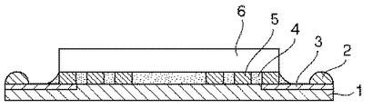
図1の半導体装置を121℃/100%/2atmRH雰囲気中に24時間及び48時間放置し、断線により異常値を示すパッケージ数/総パッケージ数を測定した。
(e)吸水率
150℃,50kgf/cm2,3分の条件で50mmφ×3mmの試験片を成形し、これを150℃,4時間の条件でポストキュアーした後、121℃/100%/2atmRH雰囲気中に24時間放置し、重量変化を測定した。
(f)吸湿後の耐半田クラック性
図1の半導体装置を121℃/100%/2atmRH雰囲気中に24時間放置した。これを240℃の半田浴に10秒間浸漬し、クラック発生パッケージ数/総パッケージ数を測定した。
(g)未硬化物の揮発成分
5gの未硬化物を180℃,1時間の条件で加熱し、重量変化を測定した。
(h)硬化物のボイド量
図1の半導体装置について、超音波探傷装置を用いて、ボイド占有面積/パッケージ総面積を測定した。
【0075】
ここで、図1において、1はBT基盤、2はAu端子、3はCu配線、4はエポキシ樹脂組成物フィルム、5は半田バンプ、6はSiチップであり、BT基盤上に、エポキシ樹脂組成物のフィルム(10mm×10mm×0.1mm)をのせ、仮圧着し、これを120℃,10秒の条件でプレヒートした後、Al配線と半田バンプを施したSiチップ(10mm×10mm×0.3mm)をのせ、180℃,10kgf/cm2,10秒の条件で加熱成形し、これを150℃,1時間の条件でポストキュアすることにより、半導体装置を作成した。
【0076】
【表3】
【表4】
【表5】
【図面の簡単な説明】
【図1】実施例、比較例で用いた半導体装置の説明図である。
【符号の説明】
1 BT基盤
2 Au端子
3 Cu配線
4 エポキシ樹脂組成物フィルム
5 半田バンプ
6 Siチップ[0001]
BACKGROUND OF THE INVENTION
The present invention relates to a self-polymerizing type or phenol-curing type epoxy resin composition, a laminated film effective for semiconductor sealing using the same, and a semiconductor device sealed with this film.
[0002]
[Prior art and problems to be solved by the invention]
In recent years, electronic devices tend to be smaller and lighter at a remarkable speed. In this trend, semiconductor devices, which are the brains of electronic devices, are also becoming smaller and lighter. Ultimately, CSP (Chip Size Package) mounting that reduces the mounting area to the chip size has been proposed. Yes.
[0003]
Epoxy resins are widely used as materials for assembling semiconductor packages because of their excellent adhesion, heat resistance, and moisture resistance. In recent years, along with the diversification of the package system as described above, it is used not only as a conventional sealing material but also as a coating material, a die bond material, an underfill material or the like. Most of these materials are diluted with a solvent or pasty.
[0004]
Of these, those diluted with a solvent have to be taken into consideration for the removal of the solvent that evaporates at the time of use from the viewpoint of the health management and safety of workers, and this is a factor for increasing the cost.
[0005]
As a method of using the coating material, a method of covering and sealing the surface of a semiconductor element only with a thin film of an epoxy resin composition, a method of screen printing with a pasty epoxy resin composition, or the like has been proposed. These materials include pastes such as conventionally known acid anhydride curable epoxy resin compositions and amine curable epoxy resin compositions, or these paste epoxy resin compositions on a film. Staged and filmed products are used.
[0006]
On the other hand, most of the die bond materials or underfill materials are conventionally paste-like materials, but recently, paste-like die bond materials made into films have been widely used. As a method of use, a film is pressure-bonded on a lead frame or a substrate, and a semiconductor element is adhered thereon and cured. Most of these materials are acid anhydride curable epoxy resin compositions and amine curable epoxy resin compositions that have been well known.
[0007]
These B-staged films are easier to handle than paste-like materials and are very promising as a method that contributes to simplification of the assembly process of semiconductor devices, but acid anhydride curable epoxy resin compositions In addition, the amine curable epoxy resin composition is insufficient as a material for directly covering the surface of the semiconductor element with a thin film because the storage stability of the uncured product and the moisture resistance and high temperature properties of the cured product are insufficient.
[0008]
On the other hand, when a self-polymerizing epoxy resin composition, particularly imidazoles are used as a curing catalyst, or in a phenol-curing epoxy resin composition, an uncured product is compared with an acid anhydride-curing type or an amine-curing type. Film with good storage stability and moisture resistance and high-temperature properties, but it is difficult to obtain a B-staged film in a semi-cured state by controlling the progress of the reaction. In order to obtain the above, it is necessary to lower the softening point of the epoxy resin or phenol resin curing agent that is a raw material, and in this case, a dilemma that the heat resistance of the cured product is insufficient occurs.
[0009]
The present invention has been made to solve the above problems, and (1) self-reducing the glass transition temperature of an uncured product without reducing the heat resistance, moisture resistance, and low stress properties of the cured product. Polymerized type and phenol curable epoxy resin composition, (2) Two or more laminated films comprising at least one thin film having good workability using a flexible epoxy resin composition of (1), and (3 ) (2) It aims at providing the semiconductor device which sealed the clearance gap between a semiconductor element and a board | substrate, and the surface of a semiconductor element with the film-form epoxy resin composition.
[0010]
Means for Solving the Problem and Embodiment of the Invention
As a result of diligent investigations to achieve the above object, the present inventor has a dinuclear content of 10% by weight or less, a total amount of 3-5 nuclei of 50% by weight or more, and a weight average molecular weight / number average molecular weight. An epoxy resin composition having an epoxy resin that is 1.7 or less, an inorganic filler, a curing catalyst, and optionally a phenol resin, and an uncured product having a softening temperature of less than 15 ° C., preferably a self-polymerizing type In this case, imidazoles are used as a curing catalyst, and in the case of a phenol curing type, a glass resin having a glass transition temperature of less than 15 ° C. and containing no monomer, more preferably, is used. An epoxide containing a copolymer obtained by reacting an aromatic polymer with an organopolysiloxane represented by the following composition formula (1), and further having a volatile component of 0.1% by weight or less. By using the resin composition, a film with very good workability can be obtained because it has good elasticity and flexibility even at room temperature, and by covering the semiconductor element with this film, heat resistance can be obtained. The present invention has been completed by finding that a semiconductor device having good moisture resistance and low stress and having a small amount of voids can be obtained.
[0011]
R a R ' b SiO (4-ab) / 2 ... (1)
(In the formula, R represents a hydrogen atom, an amino group, an epoxy group, a hydroxy group or a carboxy group containing a monovalent hydrocarbon group or an alkoxy group, and R ′ represents a substituted or unsubstituted monovalent hydrocarbon group. , A and b are positive numbers satisfying 0.001 ≦ a ≦ 1, 0.9 ≦ b ≦ 2, 1 ≦ a + b ≦ 3, and the number of silicon atoms in one molecule is 2 to 1000, (The number of functional groups R directly bonded to silicon atoms in one molecule is 1 or more.)
[0012]
Therefore, the present invention firstly
(A) A novolak type epoxy resin or a trishydroxyphenylalkane type epoxy resin selected from phenol novolac type epoxy resin, cresol novolak resin and co-condensation novolak type epoxy resin of phenol and cresol, wherein the dinuclear is 10% by weight or less The total amount of 3 to 5 nuclei is 50% by weight or more, preferably the total amount of 3 to 5 nuclei is 60% by weight or more and the proportion of the 3 nuclei in the total amount of 3 to 5 nuclei is 58.18% by weight or more 4 The content of the nucleus is 0 to 13% by weight,
An epoxy resin having a weight average molecular weight / number average molecular weight of 1.7 or less.
(B) Inorganic filler
(C) Curing catalyst
(D) Phenolic resin as required
The glass transition temperature of the uncured product is less than 15 ° C. and the thickness is 20 to 150 μm at 25 ° C. and rubbery of A self-polymerizing type or phenol-curing type epoxy resin composition characterized by being in a form;
Secondly, when the (D) component phenol resin is not contained, the curing catalyst of the (C) component is an imidazole, and the above self-polymerizing epoxy resin composition or the (D) component phenol resin is contained. A phenol novolac resin or a cresol novolak resin, the glass transition temperature of which is less than 15 ° C. and containing no monomer, the above phenol curable epoxy resin composition,
Third, the above epoxy resin composition containing a copolymer obtained by reacting an aromatic polymer with an organopolysiloxane represented by the following composition formula (1):
R a R ' b SiO (4-ab) / 2 ... (1)
(In the formula, R represents a hydrogen atom, an amino group, an epoxy group, a hydroxy group or a carboxy group containing a monovalent hydrocarbon group or an alkoxy group, and R ′ represents a substituted or unsubstituted monovalent hydrocarbon group. , A and b are positive numbers satisfying 0.001 ≦ a ≦ 1, 0.9 ≦ b ≦ 2, 1 ≦ a + b ≦ 3, and the number of silicon atoms in one molecule is 2 to 1000. (The number of functional groups R directly bonded to silicon atoms in one molecule is 1 or more.)
Fourth, the epoxy resin composition as described above, wherein the volatile component in the uncured product is 0.1% by weight or less.
I will provide a.
[0013]
The present invention also provides the above Film comprising epoxy resin composition and film A laminated film comprising a silicone sheet, a polytetrafluoroethylene sheet, a release layer or a protective layer selected from polyethylene terephthalate coated with polytetrafluoroethylene on the surface, and in this case A laminated film in which an adhesive layer is sandwiched between one or both of the epoxy resin composition and the protective layer, and the epoxy resin composition Film Provided is a semiconductor device in which a surface of a semiconductor element is sealed with a cured product.
[0014]
Hereinafter, the present invention will be described in detail.
The epoxy resin that can be used in the present invention is 10% by weight or less (ie, 0 to 10% by weight) of dinuclear body, and 50% by weight or more (ie, 50 to 100% by weight) of 3-5 cores. ) And The proportion of trinuclear body in the total amount of 3-5 nuclear bodies is 58.18 wt% or more, and the content of tetranuclear bodies is 0-13 wt%, Any epoxy resin having a weight average molecular weight / number average molecular weight of 1.7 or less (that is, 1.0 to 1.7) can be used. Here, the epoxy resin used in the present invention has one epoxy group for each nucleus, and therefore the n-nuclear body has n epoxy groups in one molecule.
[0015]
Examples of this type of epoxy resin include a novolak epoxy resin such as a phenol novolac epoxy resin represented by the following formula (2), a cresol novolac epoxy resin, or a co-condensation novolac epoxy resin of phenol and cresol, And trishydroxyphenylalkane type epoxy resins such as trishydroxyphenylmethane type epoxy resin and trishydroxyphenylpropane type epoxy resin. Among these, in particular, the total amount of 3 to 5 nuclei is 60% by weight or more (60 to 100% by weight), and the proportion of 3 nuclei in the total amount of 3 to 5 nuclei is 60% by weight or more (60 to 100% by weight), a weight average molecular weight / number average molecular weight of 1.5 or less (1.0 to 1.5), and a softening temperature of less than 15 ° C., particularly less than 10 ° C., especially phenol novolac Type epoxy resin or cresol novolac type epoxy resin is desirable. When there is too much content of a binuclear body with respect to the whole epoxy resin, the glass transition temperature of hardened | cured material will become low and will cause a heat resistant fall. In addition, even if the content of dinuclear is appropriate, if the total amount of 3-5 nuclei is too small, the ratio of hexanuclear or more increases, the glass transition temperature of the uncured product increases, There arises a problem that the flexibility is lost and the film is damaged.
[0016]
[Chemical 1]
[0017]
[Chemical formula 2]
[Chemical 3]
[0019]
[Formula 4]
In addition to the above epoxy resins, bisphenol type epoxy resins such as bisphenol A type epoxy resin and bisphenol F type epoxy resin, biphenyl type epoxy resin, naphthalene type epoxy resin, cyclopentadiene type epoxy resin, phenol aralkyl type epoxy resin, biphenyl aralkyl type A conventionally known epoxy resin such as an epoxy resin may be used in combination. In this case, the compounding amount of these epoxy resins is within a range where the glass transition temperature of the epoxy resin composition does not become 15 ° C. or higher.
[0021]
The total chlorine content in these epoxy resins is preferably 1500 ppm or less, particularly 1000 ppm or less. Moreover, it is preferable that the extraction water chlorine in 20 hours in a 50% epoxy resin density | concentration at 120 degreeC is 5 ppm or less. If the total chlorine content and the amount of extracted water chlorine are large, the moisture resistance reliability of the semiconductor may be reduced.
[0022]
The kind of the inorganic filler that can be used in the present invention is not particularly limited, and is arbitrarily selected depending on the application. For example, natural silica such as crystalline silica and non-crystalline silica, synthetic high purity silica, synthetic spherical silica, talc, mica, silicon nitride, boron nitride, alumina, etc., or conductive particles such as Ag powder, etc. Alternatively, two or more types can be used. The shape of the inorganic filler is not particularly limited, such as a spherical shape, a crushed shape, and an amorphous shape, but a spherical shape is preferable. The amount of the inorganic filler blended is the total amount of resin (that is, when the amount of epoxy resin and a copolymer of a phenol resin or an aromatic polymer and an organopolysiloxane described later are blended) It is preferably 50 to 1000 parts by weight, more preferably 100 to 400 parts by weight with respect to 100 parts by weight of the total of the amount of the polymer added. The particle size of the inorganic filler is limited by the thickness of the laminated film, and desirably the maximum particle size is less than the film thickness and the average particle size is less than 1/2.
[0023]
Usually, the maximum particle size is less than 150 μm, preferably less than 75 μm, and the average particle size is about 0.1 to 70 μm, preferably about 1 to 30 μm. This average particle diameter can be obtained, for example, as a weight average value (or median diameter) by a laser light diffraction method.
[0024]
The epoxy resin composition of the present invention can be prepared in either a self-polymerization type that does not contain a curing agent such as a phenol resin, or a phenol curing type that uses a phenol resin as a curing agent. Blended as an essential ingredient.
[0025]
In this case, the type of the curing catalyst that can be used in the self-polymerizing epoxy resin composition is not particularly limited as long as the epoxy resin is homopolymerized, and examples thereof include imidazoles and tertiary amines. Although 1 type (s) or 2 or more types can be used, it is particularly preferable to use imidazoles (imidazole compounds) in view of the storage stability of the uncured product. Examples of imidazoles include 2-methylimidazole, 2-ethylimidazole, 2-ethyl-4-methylimidazole, 2-phenylimidazole, 2-phenyl-4-methylimidazole, 2-phenyl-4-hydroxymethylimidazole, 2- Phenyl-4,5-di (hydroxymethyl) -imidazole and the like can be mentioned, and examples of tertiary amines include triethylamine, benzyldimethylamine, α-methylbenzyldimethylamine and 1,8-diazabicyclo (5.4). 0.0) cycloamidine compounds such as undecene-7.
[0026]
In the case of a phenol curable epoxy resin composition, in addition to the imidazoles and tertiary amines, triphenylphosphine, tributylphosphine, tri (p-toluyl) phosphine, tri (p-methoxyphenyl) phosphine, tri (p- Organic phosphine compounds such as ethoxyphenyl) phosphine and triphenylphosphine / triphenylborane and salts thereof, and quaternary phosphonium compounds such as tetraphenylphosphonium and tetraphenylborate and organic phosphorus compounds such as salts thereof can be used.
[0027]
The amount of curing catalyst is preferably 0.01 to 10 parts by weight, more preferably 0.1 to 100 parts by weight of epoxy resin (when phenolic resin is blended, the total amount of epoxy resin and phenolic resin). 5 parts by weight. If the blending amount of the curing catalyst is too small, curing failure may occur at the time of heat molding, and if it is too large, there may be a problem that storage stability is lowered.
[0028]
In the phenol curable epoxy resin composition, a phenol resin is blended as a curing agent.
[0029]
The phenol resin used in the present invention may be any phenol resin having at least one, preferably two or more phenolic hydroxyl groups in the molecule, and its molecular weight distribution is particularly limited like an epoxy resin. Although not intended, in order to achieve that the glass transition temperature of the epoxy resin composition (uncured product) is less than 15 ° C., the glass transition temperature of the phenol resin is desirably less than 15 ° C., particularly preferably. Is preferably less than 10 ° C. Moreover, in order to avoid that the heat resistance of hardened | cured material falls, it is desirable not to contain a monomer (namely, mononuclear body). In consideration of such conditions, the monomer (one nucleus) is not contained, the total amount of 2 to 4 nuclei is 80% by weight or more (that is, 80 to 100% by weight), and 2 to 4 The ratio of the binuclear body to the total amount of the nuclear body is 40% by weight or more and less than 70% by weight, and the glass transition temperature is less than 15 ° C., particularly less than 10 ° C., in particular phenol novolak resin or cresol novolak resin (The following structural formula (4)) is desirable. Here, the phenol resin used in the present invention has one phenolic hydroxyl group for each nucleus, and therefore the n nucleus has n phenolic hydroxyl groups in one molecule. . When the ratio of the binuclear body to the total amount of the 2-4 nuclear bodies is 70% by weight or more, the glass transition temperature of the cured product becomes low, which may cause a decrease in heat resistance. In addition, when the ratio of the dinuclear body to the total amount of the 2-4 nuclei is less than 40% by weight and the total amount of the 2-4 nuclei is less than 80% by weight, the ratio of the 3 nuclei or more increases, and the uncured product There is a possibility that the glass transition temperature of the film becomes high, the flexibility of the film is impaired at room temperature, and the film is damaged.
[0030]
[Chemical formula 5]
[0031]
In addition to the above phenol resins, bisphenol A type resins, bisphenol F type resins such as bisphenol F type resins, co-condensed novolak resins of phenol and cresol, trishydroxyphenylmethane type resins, trishydroxyphenylpropane type resins, etc. Conventionally known phenol resins such as alkane type resin, naphthalene type phenol resin, cyclopentadiene type phenol resin, phenol aralkyl resin, biphenyl aralkyl type phenol resin may be used together. In this case, the blending amount of these phenol resins is epoxy. The glass transition temperature of the resin composition is within a range not exceeding 15 ° C.
[0032]
The compounding amount of the phenol resin is 0.5 or more and 2.0 or less in an equivalent ratio (that is, molar ratio of the phenolic hydroxyl group in the phenol resin to the epoxy group in the epoxy resin) with respect to the compounding amount of the epoxy resin. Desirably, it is 0.8 or more and 1.2 or less more preferably. When the blending amount of the phenol resin is less than 0.5 or more than 2.0 in an equivalent ratio with respect to the blending amount of the epoxy resin, there is a problem that the resin composition is not sufficiently cured and the heat resistance is lowered. There is a risk.
[0033]
The epoxy resin composition of the present invention can be blended with pigments such as carbon black, dyes, flame retardants, coupling agents, thermoplastic resins and other additives depending on the application.
[0034]
The epoxy resin composition of the present invention is a flexible rubber-like material in the vicinity of room temperature (about 25 ° C.) in an uncured state, and therefore the glass transition temperature of the uncured product is less than 15 ° C., more preferably less than 10 ° C. Is desirable. When the glass transition temperature of the uncured product is 15 ° C. or higher, the flexibility of the film is impaired at room temperature, which may cause a problem that the film is damaged.
[0035]
In the epoxy resin composition of the present invention, a copolymer obtained by reacting an aromatic polymer with a specific organopolysiloxane may be blended as necessary in order to improve particularly low stress properties. desirable.
[0036]
Here, various compounds can be used as the aromatic polymer, and examples thereof include epoxy resins and phenol resins having the structures of the following formulas (5) and (6).
[0037]
[Chemical 6]
[Chemical 7]
[0039]
[Chemical 8]
Moreover, the alkenyl-group containing compound (epoxy resin or phenol resin) of the structure of following formula (7)-(9) can also be used as an aromatic polymer.
[0041]
[Chemical 9]
[0042]
[Chemical Formula 10]
On the other hand, the organopolysiloxane is represented by the following composition formula (1).
R a R ' b SiO (4-ab) / 2 ... (1)
(Wherein, R represents a hydrogen atom, an amino group, an epoxy group, a hydroxy group or a carboxy group containing a monovalent hydrocarbon group or an alkoxy group, R ′ represents a substituted or unsubstituted monovalent hydrocarbon, a and b are positive numbers satisfying 0.001 ≦ a ≦ 1, 0.9 ≦ b ≦ 2, and 1 ≦ a + b ≦ 3, where R is an epoxy group or phenol in the aromatic polymer described above. A functional group capable of reacting with a functional hydroxyl group or an alkenyl group to form a copolymer, and the number of silicon atoms in one molecule is 2-1000, preferably 10-400, The number of functional groups R directly bonded to the silicon atom is 1 or more, preferably 2 to 5, particularly preferably 2.)
[0044]
In this case, examples of the amino group-containing monovalent hydrocarbon group for R include the following.
[0045]
Embedded image
[0046]
Examples of the epoxy group-containing monovalent hydrocarbon group include the following.
[0047]
Embedded image
[0048]
Examples of the hydroxy group-containing monovalent hydrocarbon group include the following.
[0049]
Embedded image
[0050]
The carboxy group-containing monovalent hydrocarbon group is -C X H 2X COOH (X is an integer of 0 to 10) is exemplified, and examples of the alkoxy group include those having 1 to 4 carbon atoms such as a methoxy group, an ethoxy group, and an n-propoxy group.
[0051]
The substituted or unsubstituted monovalent hydrocarbon group for R ′ is preferably one having 1 to 10 carbon atoms, for example, methyl group, ethyl group, n-propyl group, isopropyl group, n-butyl group, isobutyl group. Tert-butyl group, pentyl group, neopentyl group, hexyl group, cyclohexyl group, octyl group, decyl group and other alkyl groups, vinyl group, allyl group, propenyl group, butenyl group and other alkenyl groups, phenyl group, tolyl group and the like And an aryl group such as an aryl group, a benzyl group, and a phenylethyl group, and a halogen-substituted monovalent hydrocarbon group in which part or all of the hydrogen atoms of these hydrocarbon groups are substituted with a halogen atom or the like. Among these, a methyl group, an ethyl group, a propyl group, and a phenyl group are particularly preferable.
[0052]
Further, a and b are the values described above, preferably 0.01 ≦ a ≦ 0.1, 1.8 ≦ b ≦ 2, 1.85 ≦ a + b ≦ 2.1, and the number of silicon atoms is preferably 10 It is -400, More preferably, it is 20-210.
[0053]
Examples of such organopolysiloxanes include compounds having the following structure.
[0054]
Embedded image
In the formulas (10) and (11), R ′ is the same unsubstituted or substituted monovalent hydrocarbon group as that in the formula (1), preferably a methyl group or a phenyl group, and X is an amino group, an epoxy group, a hydroxy group or A carboxy group-containing monovalent hydrocarbon group, p is an integer of 0 to 1000, preferably 8 to 400, and q is an integer of 0 to 20, preferably 0 to 5.
[0056]
Specific examples include the following diorganopolysiloxanes.
[0057]
Embedded image
Although the molecular weight of said organopolysiloxane is not specifically limited, 100-70000 are desirable. This is because, when the molecular weight of the organopolysiloxane is 100 to 70000, when the obtained copolymer is blended with the epoxy resin composition, the copolymer is not compatible with the matrix and forms a fine sea-island structure. Because. When the molecular weight is less than 100, the copolymer is compatible in the matrix, the sea-island structure disappears, and when the molecular weight is greater than 70000, the sea-island becomes large. In either case, the low stress property of the cured product is low. May decrease.
[0059]
As a method for obtaining a copolymer by reacting the aromatic polymer and organopolysiloxane, a known method is employed.
[0060]
The amount of the copolymer is preferably about 0 to 100 parts by weight, more preferably 1 to 100 parts by weight with respect to 100 parts by weight of the epoxy resin (when the phenol resin is added, the total of the epoxy resin and the phenol resin). About 50 parts by weight. In particular, in the case of a phenol curable epoxy resin composition, the total amount of phenolic hydroxyl groups is 0.5 or more and 2.0 with respect to the total amount of epoxy groups in the entire epoxy resin, phenol resin and copolymer. Or less, more preferably 0.8 or more and 1.2 or less. When the total amount of phenolic hydroxyl groups is out of the above range with respect to the total amount of epoxy groups, there may be a problem that the resin composition is not sufficiently cured and heat resistance is lowered.
[0061]
The epoxy resin composition of the present invention uniformly stirs and mixes the above-mentioned predetermined amounts of the components, and after mixing with a roll, kneader, continuous kneader or the like that has been heated to 70 to 90 ° C. in advance, the glass transition temperature or lower It can be obtained by a method such as cooling and crushing. In addition, the mixing order of the components is not particularly limited.
[0062]
Although the epoxy resin composition of the present invention is preferably used in the form of a film, the conditions during the heat molding in this case are such that the pressure applied to the material is extremely small compared to the conventional solid resin transfer molding, In addition, compared with potting or underfilling of a liquid material, the material is often exposed to a high temperature rapidly. Therefore, since the volatile component contained in the uncured product tends to remain as a void after curing, it is desired that the volatile component is extremely small. Specifically, it is desirable that the content of the volatile component is 0.1% by weight or less, preferably 0.01% by weight or less.
[0063]
The epoxy resin composition of the present invention is effectively used for semiconductor encapsulation, but is preferably used after being processed into a film, and particularly preferably used as at least one layer of two or more laminated films. . In this case, the thickness of the film made of the epoxy resin composition of the present invention is preferably 20 to 150 μm. In addition, the material, thickness, etc. of another layer are selected according to the use of a laminated film.
[0064]
Specifically, for the purpose of protecting the layer formed of the epoxy resin composition of the present invention, a silicone sheet, a Teflon sheet, or a PET (polyethylene terephthalate) sheet coated on the surface with a release silicone or Teflon, etc. A laminated film with one or both surfaces attached, a pressure-sensitive adhesive layer for temporary adhesion to a substrate or a semiconductor element at room temperature on one or both of the epoxy resin composition layer and the protective layer A laminated film or the like sandwiched between them.
[0065]
The laminated film of the present invention is manufactured using a coater / laminator or the like used for manufacturing a normal rubber sheet. At this time, the epoxy resin composition of the present invention can be produced by heating and pressurizing and stretching as necessary, and cutting into a plate shape or cutting into a tape shape and winding depending on the use of the laminated film. This is further cut | disconnected according to a use, and is used after removing the protective layer mentioned above.
[0066]
The semiconductor device in which the laminated film of the present invention is used is not particularly limited, but is suitable for a small and thin semiconductor device such as a CSP, and particularly for use in an adhesive having a narrow gap between a chip and a substrate. It is effective and can provide an adhesive having higher reliability than a conventional acid anhydride curable material or amine curable material. Also, the method of using the laminated film of the present invention is not particularly limited, but the film is cut into an appropriate size, temporarily pressure-bonded on the substrate, a chip is mounted on the film, and then the whole is heat-bonded. A semiconductor device can be obtained by such a method. Here, the film may be preheated before the chip is mounted.
[0067]
【The invention's effect】
In the epoxy resin composition of the present invention, by controlling the molecular weight distribution of the epoxy resin (and preferably the phenol resin curing agent), the glass transition of the uncured product without reducing the heat resistance and moisture resistance of the cured product. It is possible to reduce the temperature. Further, by using this epoxy resin composition, a flexible film having good workability can be obtained. Further, the epoxy resin composition layer is one layer, and other layers are pasted depending on the application. A laminated film of more than one layer can be obtained, and a semiconductor device having good heat resistance, moisture resistance, and low stress can be obtained by covering a semiconductor element with this film.
[0068]
【Example】
EXAMPLES Hereinafter, although an Example and a comparative example are given and this invention is demonstrated concretely, this invention is not limited to the following Example.
[0069]
[Examples and Comparative Examples]
Epoxy resins A to F having molecular weight distribution, epoxy equivalent and glass transition temperature shown in Table 1, phenol resins A to D having molecular weight distribution, phenolic hydroxyl group equivalent and glass transition temperature shown in Table 2, inorganic filler ( Spherical silica having a maximum particle size of less than 24 μm and an average particle size of 4 μm), a curing catalyst (2-phenylimidazole 2PZ or triphenylphosphine TPP), a silane coupling agent (γ-glycidoxypropyltrimethoxysilane, KBM403: manufactured by Shin-Etsu Chemical) And a compound represented by the following formula (a copolymer of an aromatic polymer and an organopolysiloxane, an epoxy equivalent of 291 and a siloxane content of 31.2% by weight) as shown in Tables 3 to 5. The blend is uniformly melt-mixed with two heat rolls, and epoxy resin compositions (Examples 1 to 10, Comparative Examples 1 to 5) are prepared. And elephants. In addition, the compounding ratio of the epoxy resin, the phenol resin, and the copolymer is epoxy group / phenolic hydroxy group = 1/1 (molar ratio), and the polysiloxane content in the copolymer with respect to the entire resin component is 8 It adjusted so that it might become weight%.
[0070]
Comparative Examples 6 and 7 are liquid bisphenol A type epoxy resin (epoxy resin G, epoxy equivalent 179) as an epoxy resin, and DDM (4,4′-diaminodiphenylmethane, equivalent 99) as a curing agent in Comparative Example 6. In Comparative Example 7, 4-MTHPA (4-methyltetrahydrophthalic anhydride, equivalent 166) was used. As shown in Table 5, this was mixed by blending (also blended so that the functional groups were equivalent), and the resulting epoxy resin composition was B-staged at about 60 ° C., as shown in Table 5 After the glass transition temperature was reached, film forming and other operations were performed.
[0071]
Embedded image
[Table 1]
E: Phenol novolac type epoxy resin
F: Trishydroxyphenylmethane type epoxy resin
Unit: 2 to 5 nuclei, 6 or more nuclei Weight%
Mw: weight average molecular weight, Mn: number average molecular weight
[0073]
[Table 2]
D: Phenol novolac resin
Unit: 2-4 nuclei, more than 5 nuclei Weight%
Mw: weight average molecular weight, Mn: number average molecular weight
[0074]
These epoxy resin compositions were subjected to the following tests (a) to (h). The results are shown in Tables 3-5.
(A) Glass transition temperature (Tg) of uncured product
Using 10 mg of uncured material, the maximum point of specific heat when the temperature was raised at 5 ° C. per minute by DCS was measured.
(B) Film handling
A strip-shaped uncured film of 10 mm × 50 mm × 0.1 mm was folded in two so that the short sides (10 mm) of the strips overlap at 25 ° C., and the number of damaged films / total number of films was measured.
(C) Glass transition temperature (Tg) of the cured product
150 ° C, 50kgf / cm 2 A test piece of 5 mm × 5 mm × 15 mm was molded under conditions of 3 minutes, post-cured at 150 ° C. for 4 hours, and then heated at 5 ° C./minute with TMA (Thermal Mechanical Analysis). The value was measured.
(D) Moisture resistance
The semiconductor device of FIG. 1 was left in an atmosphere of 121 ° C./100%/2 atmRH for 24 hours and 48 hours, and the number of packages showing abnormal values due to disconnection / total number of packages was measured.
(E) Water absorption rate
150 ° C, 50kgf / cm 2 , A 50 mmφ x 3 mm test piece was molded under the condition of 3 minutes, post-cured at 150 ° C for 4 hours, and then left in an atmosphere of 121 ° C / 100% / 2 atmRH for 24 hours to measure the weight change. did.
(F) Resistance to solder cracks after moisture absorption
The semiconductor device of FIG. 1 was left in an atmosphere of 121 ° C./100%/2 atmRH for 24 hours. This was immersed in a solder bath at 240 ° C. for 10 seconds, and the number of crack generation packages / total number of packages was measured.
(G) Volatile component of uncured product
5 g of uncured material was heated at 180 ° C. for 1 hour, and the change in weight was measured.
(H) Void amount of cured product
For the semiconductor device of FIG. 1, the void occupation area / total package area was measured using an ultrasonic flaw detector.
[0075]
Here, in FIG. 1, 1 is a BT substrate, 2 is an Au terminal, 3 is a Cu wiring, 4 is an epoxy resin composition film, 5 is a solder bump, 6 is a Si chip, and an epoxy resin composition is formed on the BT substrate. An article film (10 mm × 10 mm × 0.1 mm) was placed, temporarily pressure-bonded, preheated at 120 ° C. for 10 seconds, and then subjected to Si wiring (10 mm × 10 mm × 0.00 mm) with Al wiring and solder bumps. 3mm), 180 ° C, 10kgf / cm 2 The semiconductor device was fabricated by heat-molding under conditions of 10 seconds and post-curing under conditions of 150 ° C. for 1 hour.
[0076]
[Table 3]
[Table 4]
[Table 5]
[Brief description of the drawings]
FIG. 1 is an explanatory diagram of a semiconductor device used in examples and comparative examples.
[Explanation of symbols]
1 BT base
2 Au terminal
3 Cu wiring
4 Epoxy resin composition film
5 Solder bump
6 Si chip
Claims (12)
(B)無機質充填材
(C)硬化触媒
を必須成分として含有し、未硬化物のガラス転移温度が15℃未満であり、厚みが20〜150μmの25℃でゴム状の形態のエポキシ樹脂組成物。(A) A novolak type epoxy resin or a trishydroxyphenylalkane type epoxy resin selected from phenol novolac type epoxy resin, cresol novolak resin and co-condensation novolak type epoxy resin of phenol and cresol, wherein the dinuclear is 10% by weight or less The total amount of 3 to 5 nuclei is 50% by weight or more, and the ratio of 3 nuclei to the total amount of 3 to 5 nuclei is 58.18% by weight or more, and the content of 4 nuclei is 0. It contains ˜13 wt% epoxy resin (B) inorganic filler (C) curing catalyst whose weight average molecular weight / number average molecular weight is 1.7 or less as an essential component, and the glass transition temperature of the uncured product is less than 15 ° C., thickness rubbery form of the epoxy resin composition at 25 ° C. of 20 to 150 [mu] m.
RaR’bSiO(4-a-b)/2 …(1)
(但し、式中Rは水素原子、アミノ基、エポキシ基、ヒドロキシ基もしくはカルボキシ基を含有する1価炭化水素基又はアルコキシ基を示し、R’は置換もしくは非置換の1価炭化水素基を示し、a、bは0.001≦a≦1、0.9≦b≦2、1≦a+b≦3を満足する正数である。また、1分子中のケイ素原子の数は2〜1000であり、1分子中のケイ素原子に直結した官能基Rの数は1以上である。)The epoxy according to any one of claims 1 to 6, wherein the epoxy resin composition contains a copolymer obtained by reacting an aromatic polymer with an organopolysiloxane represented by the following composition formula (1). Resin composition.
R a R ′ b SiO (4-ab) / 2 (1)
Wherein R represents a hydrogen atom, an amino group, an epoxy group, a hydroxy group or a carboxy group containing a monovalent hydrocarbon group or an alkoxy group, and R ′ represents a substituted or unsubstituted monovalent hydrocarbon group. , A and b are positive numbers satisfying 0.001 ≦ a ≦ 1, 0.9 ≦ b ≦ 2, 1 ≦ a + b ≦ 3, and the number of silicon atoms in one molecule is 2 to 1000. (The number of functional groups R directly bonded to silicon atoms in one molecule is 1 or more.)
Priority Applications (1)
| Application Number | Priority Date | Filing Date | Title |
|---|---|---|---|
| JP25844499A JP3672011B2 (en) | 1998-09-25 | 1999-09-13 | Epoxy resin composition and laminated film and semiconductor device using this epoxy resin composition |
Applications Claiming Priority (5)
| Application Number | Priority Date | Filing Date | Title |
|---|---|---|---|
| JP27083498 | 1998-09-25 | ||
| JP10-270834 | 1998-09-25 | ||
| JP10-350932 | 1998-12-10 | ||
| JP35093298 | 1998-12-10 | ||
| JP25844499A JP3672011B2 (en) | 1998-09-25 | 1999-09-13 | Epoxy resin composition and laminated film and semiconductor device using this epoxy resin composition |
Publications (2)
| Publication Number | Publication Date |
|---|---|
| JP2000230113A JP2000230113A (en) | 2000-08-22 |
| JP3672011B2 true JP3672011B2 (en) | 2005-07-13 |
Family
ID=27334723
Family Applications (1)
| Application Number | Title | Priority Date | Filing Date |
|---|---|---|---|
| JP25844499A Expired - Fee Related JP3672011B2 (en) | 1998-09-25 | 1999-09-13 | Epoxy resin composition and laminated film and semiconductor device using this epoxy resin composition |
Country Status (1)
| Country | Link |
|---|---|
| JP (1) | JP3672011B2 (en) |
Cited By (1)
| Publication number | Priority date | Publication date | Assignee | Title |
|---|---|---|---|---|
| KR20230029315A (en) * | 2021-08-24 | 2023-03-03 | 한국다이요잉크 주식회사 | Uv curable type ink-jet ink composition |
Families Citing this family (7)
| Publication number | Priority date | Publication date | Assignee | Title |
|---|---|---|---|---|
| JP3672009B2 (en) * | 1999-04-14 | 2005-07-13 | 信越化学工業株式会社 | Epoxy resin composition and laminated film and semiconductor device using this epoxy resin composition |
| JP5254590B2 (en) * | 2007-10-17 | 2013-08-07 | 昭和電工株式会社 | Low molecular weight novolak resin, method for producing the same, and thermosetting resin composition using the same |
| JP2011014717A (en) * | 2009-07-02 | 2011-01-20 | Sumitomo Bakelite Co Ltd | Adhesive film, multilayer circuit board, electronic component and semiconductor device |
| JP2012146830A (en) * | 2011-01-12 | 2012-08-02 | Sumitomo Bakelite Co Ltd | Adhesive sheet integrating dicing tape, electronic component and semiconductor device |
| JP2015174874A (en) * | 2014-03-13 | 2015-10-05 | 信越化学工業株式会社 | Resin composition for encapsulating semiconductor and semiconductor device |
| JP2016108561A (en) * | 2014-12-04 | 2016-06-20 | 日東電工株式会社 | Soft magnetic resin composition and soft magnetic film |
| CN115050987B (en) * | 2022-06-28 | 2024-06-14 | 睿得新材料科技(佛山)有限公司 | Sealing material for protecting fuel cell membrane electrode and preparation method thereof |
-
1999
- 1999-09-13 JP JP25844499A patent/JP3672011B2/en not_active Expired - Fee Related
Cited By (1)
| Publication number | Priority date | Publication date | Assignee | Title |
|---|---|---|---|---|
| KR20230029315A (en) * | 2021-08-24 | 2023-03-03 | 한국다이요잉크 주식회사 | Uv curable type ink-jet ink composition |
Also Published As
| Publication number | Publication date |
|---|---|
| JP2000230113A (en) | 2000-08-22 |
Similar Documents
| Publication | Publication Date | Title |
|---|---|---|
| TWI332521B (en) | Adhesive films for semiconductor | |
| JP5549559B2 (en) | Adhesive composition, method for producing the same, adhesive film using the same, substrate for mounting semiconductor, and semiconductor device | |
| US6512031B1 (en) | Epoxy resin composition, laminate film using the same, and semiconductor device | |
| KR102295921B1 (en) | Resin composition, resin film, and semiconductor device and method for manufacturing same | |
| JP4892164B2 (en) | Liquid epoxy resin composition and electronic component device | |
| US6210811B1 (en) | Epoxy resin composition, laminate film using the same, and semiconductor device | |
| US20180247834A1 (en) | Method for manufacturing semiconductor apparatus | |
| US9449856B2 (en) | Encapsulant with base for use in semiconductor encapsulation, semiconductor apparatus, and method for manufacturing semiconductor apparatus | |
| JP2001288340A (en) | Sealing material for flip-chip type semiconductor device and flip-chip type semiconductor device | |
| KR101904509B1 (en) | Liquid epoxy resin composition for semiconductor sealing and resin-sealed semiconductor device | |
| JP6754741B2 (en) | Semiconductor laminates, methods for manufacturing semiconductor laminates, and methods for manufacturing semiconductor devices | |
| JP3672009B2 (en) | Epoxy resin composition and laminated film and semiconductor device using this epoxy resin composition | |
| KR102262042B1 (en) | Base-attached encapsulant for semiconductor encapsulation, semiconductor apparatus, and method for manufacturing semiconductor apparatus | |
| TWI846922B (en) | Multilayer sheet for mold bottom filling packaging, mold bottom filling packaging method, electronic component mounting substrate and electronic component mounting substrate manufacturing method | |
| JP2004319823A (en) | An adhesive film for a semiconductor, a semiconductor device, and a method for manufacturing a semiconductor device. | |
| JP3723461B2 (en) | Electronic component equipment | |
| JP3796648B2 (en) | Epoxy resin composition, and laminated film and semiconductor device using this epoxy resin composition | |
| CN111630126B (en) | Adhesive composition, film adhesive, adhesive sheet and method for producing semiconductor device | |
| CN105637623A (en) | Adhesive film for semiconductor bonding | |
| JP3672011B2 (en) | Epoxy resin composition and laminated film and semiconductor device using this epoxy resin composition | |
| JPWO2007029504A1 (en) | Epoxy resin composition and die-bonding agent containing the composition | |
| TWI748126B (en) | Resin composition, resin film, semiconductor laminate, semiconductor laminate manufacturing method, and semiconductor device manufacturing method | |
| JP6286959B2 (en) | Epoxy resin composition, electronic component device, and method of manufacturing electronic component device | |
| JP2000299414A (en) | Flip chip type semiconductor device | |
| JP2015054952A (en) | Epoxy resin composition, electronic component device, and method of manufacturing electronic component device |
Legal Events
| Date | Code | Title | Description |
|---|---|---|---|
| A977 | Report on retrieval |
Free format text: JAPANESE INTERMEDIATE CODE: A971007 Effective date: 20040611 |
|
| A131 | Notification of reasons for refusal |
Free format text: JAPANESE INTERMEDIATE CODE: A131 Effective date: 20040804 |
|
| A521 | Request for written amendment filed |
Free format text: JAPANESE INTERMEDIATE CODE: A523 Effective date: 20040928 |
|
| A131 | Notification of reasons for refusal |
Free format text: JAPANESE INTERMEDIATE CODE: A131 Effective date: 20050105 |
|
| A521 | Request for written amendment filed |
Free format text: JAPANESE INTERMEDIATE CODE: A523 Effective date: 20050302 |
|
| TRDD | Decision of grant or rejection written | ||
| A01 | Written decision to grant a patent or to grant a registration (utility model) |
Free format text: JAPANESE INTERMEDIATE CODE: A01 Effective date: 20050330 |
|
| A61 | First payment of annual fees (during grant procedure) |
Free format text: JAPANESE INTERMEDIATE CODE: A61 Effective date: 20050412 |
|
| R150 | Certificate of patent or registration of utility model |
Ref document number: 3672011 Country of ref document: JP Free format text: JAPANESE INTERMEDIATE CODE: R150 Free format text: JAPANESE INTERMEDIATE CODE: R150 |
|
| FPAY | Renewal fee payment (event date is renewal date of database) |
Free format text: PAYMENT UNTIL: 20080428 Year of fee payment: 3 |
|
| FPAY | Renewal fee payment (event date is renewal date of database) |
Free format text: PAYMENT UNTIL: 20110428 Year of fee payment: 6 |
|
| LAPS | Cancellation because of no payment of annual fees |