JP3671740B2 - Reflective liquid crystal display - Google Patents
Reflective liquid crystal display Download PDFInfo
- Publication number
- JP3671740B2 JP3671740B2 JP13537899A JP13537899A JP3671740B2 JP 3671740 B2 JP3671740 B2 JP 3671740B2 JP 13537899 A JP13537899 A JP 13537899A JP 13537899 A JP13537899 A JP 13537899A JP 3671740 B2 JP3671740 B2 JP 3671740B2
- Authority
- JP
- Japan
- Prior art keywords
- liquid crystal
- crystal display
- reflective
- string
- display device
- Prior art date
- Legal status (The legal status is an assumption and is not a legal conclusion. Google has not performed a legal analysis and makes no representation as to the accuracy of the status listed.)
- Expired - Fee Related
Links
Images


Description
【0001】
【発明の属する技術分野】
本発明は液晶表示装置に係り、特に反射型カラー表示に有効な機能を備えた液晶表示装置に関するものである。
【0002】
【従来の技術】
従来の反射型カラー液晶表示装置として、特開平4−243226 号公報および特開平10−177106号公報に示されるように、円形状で断面形状の傾斜角分布が対称な凸部あるいは凹部を反射膜下に形成し、あらゆる方向から入射される光を、観察者の方向に集光させるようにした反射板を液晶素子内に備えた液晶表示装置が提案されている。
【0003】
また、前記従来技術では、光の干渉を発生させないように、円形状の凸部あるいは凹部を不規則に配置させた、微細で多数の凹凸反射面を有する反射板も開示されている。
【0004】
さらに、特開平10−177106号公報に示されるように、円形状で断面形状の傾斜角分布が非対称な凸部あるいは凹部を反射膜下に形成し、入射光を特定の方向に集光させるようにした反射板を液晶素子内に備えた液晶表示装置も提案されている。
【0005】
【発明が解決しようとする課題】
前記従来技術は、画素電極部に対応する領域内に円形状の凸部あるいは凹部を不規則に配置することにより光の干渉による色付きを防止するため、円形状の凸部あるいは凹部を最密充填配置した時よりも入射光を制御するための反射要素である凸部あるいは凹部の数が大幅に減少し、表示が暗いという課題を有していた。
【0006】
また、前記従来技術は、円形状の凸部あるいは凹部の傾斜角分布を非対称にすることで反射光を特定の方向に集光させるため、製作プロセスが複雑になり、微細な凸部あるいは凹部の形状制御が難しいという課題もあった。
【0007】
さらに、上記従来技術は、円形状の微細な凸部あるいは凹部をフォトリソグラフィ法で形成するため、製作プロセスが複雑でその工程も多く、コスト高になるという課題も有していた。
【0008】
本発明の目的は、上記課題を解決し、より良好な反射特性を有する反射板を備えた反射型液晶表示装置およびその製造方法を提供することにある。
【0009】
【課題を解決するための手段】
本発明は、ガラス基板上に凹凸を有する樹脂層と反射層が積層された構成の反射板を内蔵する反射型液晶表示装置であって、上記目的を達成するため、1)滑らかな曲線をもつ紐状の凸部あるいは紐状の凹部を連続、かつ交互に配置、2)滑らかな曲線をもつ紐状の凸部を連続的に配置、3)滑らかな曲線をもつ紐状の凹部を連続的に配置すること等により樹脂層に微小な凹凸面を形成した反射板を内蔵することを特徴とする反射型液晶表示装置である。
【0010】
また、本発明の反射板は紐状凸部あるいは紐状凹部が長さ方向に対して直角方向の断面形状の傾斜角分布がほぼ左右対称で、かつ各方位において前記紐状凸部あるいは紐状凹部の長さの総和がほぼ等しくなるように配置することにより樹脂層に微小な凹凸面を形成したことを特徴とする反射型液晶表示装置用内蔵反射板である。
【0011】
さらに、本発明の反射板は紐状凸部あるいは紐状凹部が長さ方向に対して直角方向の断面形状の傾斜角分布がほぼ左右対称で、かつ各方位において前記紐状凸部あるいは紐状凹部の長さの総和が異なるように配置することにより樹脂層に微小な凹凸面を形成したことを特徴とする反射型液晶表示装置用内蔵反射板である。
【0012】
また、本発明は、ガラス基板上に前記紐状の凸部あるいは紐状の凹部からなる微小な凹凸面を有する樹脂層,反射層,絶縁層,透明電極、配向制御膜が積層された一方の電極基板と、他方のガラス上に遮光層,着色層,平坦化層,透明電極,配向制御が積層された他方の電極基板とが、液晶を介して互いの透明電極が対向するように配置された素子構造とすることを特徴とする反射型液晶表示装置である。
【0013】
また、本発明は、ガラス基板上に前記紐状の凸部あるいは紐状の凹部からなる微小な凹凸面を有する黒色顔料等が分散された樹脂層,画素に対応する部分にのみ配置された短冊状の反射着,着色層,平坦化層,透明電極,配向制御膜が積層された一方の電極基板と、他方のガラス基板上に透明電極,配向制御膜が積層された他方の電極基板とが、液晶を介して互いの透明電極が対向するように配置された素子構造とすることを特徴とする反射型液晶表示装置である。
【0014】
また、本発明は、前記凸部あるいは凹部からなる凹凸パターンをスピノーダル分解による相分離パターン生成のシミュレーション手法により形成することを特徴とするものであり、前記樹脂層を形成する際に使用するフォトマスクの遮光パターン、あるいは転写用金型に形成される凹凸パターンのマスターパターン等に用いることを特徴とする。
【0015】
さらに、本発明は、スピノーダル分解によるパターン生成のシミュレーション手法が、1)Cahn-Hilliard-Cook方程式,2)時間依存Ginzburg-Landau方程式,3)Cell-Dyamical-System方程式等を用いた数値シミュレーションであることを特徴とするものである。
【0016】
さらに、本発明の反射板形成に用いるフォトマスク用の遮光部パターンあるいは透過部パターンは、スピノーダル分解のシミュレーションにより生成されたパターンか、または前記パターンをコンピュータ等に取込んで画像処理されたパターンのいずれかであることを特徴するものである。
【0017】
さらに、本発明は、前記シミュレーション手法により生成されるパターンが、あらゆる方位に対して一様な反射特性を示すものか、あるいは入射光を特定の方向に集光させるような反射特性を示すものの、いずれかであることを特徴とするものである。
【0018】
本発明の反射型液晶表示装置は、ガラス基板の一方の面に、最密充填配置が可能な前記紐状パターンからなる滑らかな凹凸面を有する樹脂層上に形成される反射膜と、その反射膜上に絶縁層,複数の透明電極,配向制御膜が積層されてなる反射電極基板と、他方のガラス基板の一方の面に遮光層,着色層,平坦化層,複数の透明電極および配向制御膜が積層されてなるカラーフィルタ基板と、前記反射電極基板とカラーフィルタ基板との間隙部に封入された液晶とを備えた液晶表示素子を用いることを特徴とするものである。
【0019】
また、本発明の反射型液晶表示素子の製造方法は、ガラス基板上に感光性樹脂を塗布する工程,前記条件を満たす凸部あるいは凹部を有する転写用型ロールあるいは型プレート等を用いて、紐状の凸部および凹部からなる滑らかな凹凸面を有する樹脂層を形成する工程,前記樹脂層上に反射膜を形成する工程,前記反射膜上に絶縁層を形成する工程,前記絶縁層上に透明電極を形成する工程,前記透明電極上に配向制御膜を形成する工程とからなる反射電極基板と、
他方のガラス基板の一方の面に遮光層を形成する工程,前記遮光層上に着色層を形成する工程,前記着色層上に平坦化層を形成する工程,前記平坦化層上に透明電極を形成する工程,前記透明電極上に配向制御を形成する工程とからなる着色層基板と、
前記反射電極基板と前記カラーフィルタ基板との間隙部に液晶を封入・封止する工程を含むことを特徴とする前記の液晶表示素子の製造方法である。
【0020】
さらに、本発明の反射型液晶表示装置の製造方法は、1)滑らかな曲線を有する紐状のパターン、2)紐状の凸部および凹部は凸部と凹部が連続的に配置、あるいは凸部または凹部が連続的に配置されたパターン、3)各方位における凸部および凹部の長さ成分の総和がほぼ等しいパターン、または、各方位における凸部および凹部の長さ成分の総和が異なるパターン、これらの条件を満たすように形成された滑らかな凹凸面を有する樹脂層が形成されたガラス基板上に反射膜を形成した反射板を有する反射型液晶表示装置の製造方法であって、前記反射板を構成するガラス基板の一方の面に感光性樹脂を塗布し、上記条件を満たすようにパターンが形成された転写用型ロールあるいは型プレートを用いて前記感光性樹脂をパターン化することにより、滑らかな凹凸面を有する樹脂層を形成する工程,凹凸面を有する前記樹脂層を形成した基板に光照射や熱処理により滑らかな凹凸面に整形する工程,滑らかな凹凸面を有する前記樹脂層上に反射膜を形成する工程と、前記反射膜上に平坦化層を形成する工程,前記平坦化膜上に複数の透明電極を形成する工程,前記透明電極上に配向制御膜を形成する工程とからなる反射電極基板と、
他方のガラス基板上に遮光層を形成する工程,前記遮光膜上に着色層を形成する工程,前記着色層上に平坦化層を形成する工程,前記平坦化層上に複数の透明電極を形成する工程,前記透明電極上に配向制御膜を形成する工程とからなる着色層基板とを、互いの配向制御膜が対向するように組合わせる工程、前記反射電極基板と前記着色層基板との間隙部に液晶を封入・封止する工程とにより液晶表示素子を作製し、
前記液晶表示素子の着色層が形成されたガラス基板の他方の面に所定の位相板と偏光板を貼り合わせる工程、前記液晶表示素子に液晶駆動用ICが搭載されたテープ・キャリア・パッケージ(以下、TCPと称する)および駆動用外部回路とを接続する工程,前記液晶表示素子をフレーム,ケース等に組み込む工程、を含むことを特徴とするものである。
【0021】
また、本発明の反射型液晶表示装置の別の製造方法は、多数の微細な凸部あるいは凹部が形成されたガラス基板上に反射膜を形成した反射板を有する反射型液晶表示装置の製造方法であって、前記反射板を構成するガラス基板の一方の面に感光性樹脂を塗布した後、遮光領域あるいは透過領域がほぼ一様な幅と所定の長さをもつ滑らかな曲線を有する紐状パターンで、かつ各方位における前記遮光領域あるいは透過領域の長さ成分の総和がほぼ等しくなるように、スピノーダル分解によるシミュレーションを用いてパターン形成された遮光手段を介して、前記感光性樹脂を露光,現像した後に熱処理してパターン化することにより、紐状の凸部および凹部が連続、かつ交互に配置された滑らかな凹凸面を有する樹脂層を形成する工程,凹凸面を有する前記樹脂層上に反射膜を形成する工程,前記反射膜上に平坦化層を形成する工程,前記平坦化膜上に複数の透明電極を形成する工程、とからなる反射電極基板と、
他方のガラス基板上に遮光層を形成する工程,前記遮光膜上に着色層を形成する工程,前記着色層上に平坦化層を形成する工程,前記平坦化層上に複数の透明電極を形成する工程とからなるカラーフィルタ基板とを、互いの透明電極が対向するように組合わせる工程,前記反射電極基板と該着色層基板との間隙部に液晶を封入・封止する工程とにより液晶表示素子を作製し、
前記液晶表示素子の着色層が形成されたガラス基板の他方の面に所定の位相板と偏光板を貼り合わせる工程,前記液晶表示素子に液晶駆動用ICが搭載されたテープ・キャリア・パッケージ(以下、TCPと称する)および駆動用外部回路とを接続する工程,前記液晶表示素子をフレーム,ケース等に組み込む工程、により完成するものである。
【0022】
【発明の実施の形態】
本発明の新規パターンを有する内蔵拡散反射板を備えた反射型カラー液晶表示装置の具体的な素子構成の一例は次の通りである。
【0023】
(1)スピノーダル分解のシミュレーションにより、紐状の凸部,凹部のパターンを生成する。ここで、スピノーダル分解のシミュレーションを行うための、スピノーダル分解のモデル方程式とは数1で与えられるCahn-Hilliard(-Cook)方程式、数2で与えられる時間依存Ginzburg-Landau方程式などがある。
【0024】
【数1】
【数2】
また、数3に示されるCell-Dynamical-System(CDS)によるスピノーダル分解モデル(拡大ムーア近傍)の数値シミュレーションによってスピノダル分解を模擬したパターンを生成することができる。
【0027】
【数3】
これらいずれかを用いることにより1)ほぼ一様な線幅をもち、かつ滑らかな曲線を有する紐状の凸および凹状パターンからなり、2)紐状の凸部あるいは凹部が連続、または交互に配置され、3)紐状の凸部および凹部の長さ方向に直角な方向の断面形状の傾斜角分布が大略左右対称であり、4)各方位において凸部および凹部の長さの総和がほぼ等しいか、または5)各方位において凸部および凹部の長さの総和が異なる、等の条件を満たす多数の滑らかな凹凸パターンを形成することができる。
【0029】
このような紐状の凸部又は凹部から構成されたパターンを転写用ロールあるいはプレート等を用いて、ガラス基板上に塗布された感光性樹脂(膜厚:0.5〜2.5μm)に前記転写用ロール(ロール速度:0.1〜3m/分)あるいはプレート等により形成された樹脂パターンに光(波長:365nm,光量:50〜500mj/cm2),熱(50〜150℃)および圧力(1〜12kg/cm2)を加えて、前記感光性樹脂をパターン化する工程、あるいはガラス基板上に塗布された感光性樹脂(膜厚:0.5〜2.5μm)にスピノーダル分解によるパターン生成のシミュレーション手法を用いて作製した紐状パターンを遮光パターンあるいは透過パターンとしたフォトマスクを介して露光(波長:365nm、光量:50〜500mj/cm2 )し、所定の現像、硬化して前記感光性樹脂をパターン化(幅:5〜20μm、高さあるいは深さ:0.5〜2.0μm)する工程、
(2)パターン化された前記樹脂層上に反射膜(アルミニウム,アルミニウム合金,銀,銀合金等の薄膜、膜厚:100〜300nm)を形成する工程、
(3)前記反射膜上に絶縁層(アクリル系感光性樹脂あるいは非感光性樹脂,膜厚:1.0〜3.0μm)を形成する工程、
(4)前記絶縁層上に透明電極を膜付け(ITO(Indium Tin Oxide),膜厚:100〜300nm),パターニング(電極数:1920本,ピッチ:100μm、電極々間隙:8〜20μm)する工程、
(5)前記透明電極上に配向制御膜(ポリイミド,膜厚:50〜100nm,温度:230〜250℃)を形成する工程から成る一方の電極基板と、
ガラス基板上に
(6)遮光層(黒色顔料分散型感光性樹脂,3層クロム等の低表面反射遮光膜 膜厚:0.1〜1.2μm,ピッチ:100μm,幅:10〜25μm)を形成する工程、
(7)前記遮光層上に着色層(赤,緑,青またはシアン,マゼンタ,イエロー,顔料分散型アクリル系感光性樹脂,膜厚:0.5〜1.5μm,ピッチ:100μm,幅:75〜90μm)を形成する工程、
(8)前記着色層上に平坦化膜(アクリル系感光性樹脂,膜厚:1.0〜3.0μm,硬化温度:230〜250℃/1hour)を形成する工程、
(9)前記平坦化膜上に透明電極を膜付け(ITO(Indium Tin Oxide),膜厚:100〜300nm),パターニング(電極数:240本,ピッチ:300μm,電極々間隙:8〜20μm)する工程、
(10)前記透明電極上に配向制御膜(ポリイミド,膜厚:50〜150nm,硬化温度:230〜250℃)を形成する工程、から成るもう一方の電極基板とを、
(11)互いの配向制御膜面が対向するようにスペーサ材(ポリマビーズ,シリカビーズ,ガラスファイバ,粒径:6μm)を介して組合わせ、両電極基板周辺をシール材(エポキシ樹脂中に上記スペーサ材を分散したもの)で接着,シールする工程、
(12)両電極基板間に液晶を封入,封止する工程、により液晶表示素子を作成する。
【0030】
そして、
(13)前記液晶表示素子の反射板が形成されていない方のガラス基板に所定の位相板と偏光板を貼り合わせる工程、
(14)前記液晶表示素子に液晶駆動用ICが搭載されたテープ・キャリア・パッケージ(以下、TCPと称する)および駆動用外部回路とを接続する工程、
(15)前記液晶表示素子をフレーム,ケース等に組み込む工程、
により本発明の液晶表示装置が完成する。
【0031】
本発明によれば、あらゆる方向から入射される光あるいは特定の方向から入射される光を、できるだけ多く観察者側に反射させるための紐状の凸部および凹部が画素電極に対応する部分に、紐状の凸部あるいは紐状の凹部が最も密になるように配置された滑らかな凹凸面を有する反射板を内蔵しているので、明るい表示の反射型液晶表示装置が提供できる。
【0032】
また、本発明によれば、前記凸部および凹部からなる紐状の凹凸パターンを形成する転写用ロール,プレートあるいはフォトマスク等の原パターンとして、高分子ブロック重合体等の相分離現象で知られるスピノーダル分解を解析するためのコンピュータシミュレーション手法により得られる相分離生成パターンを用いるため、不規則な配列パターンで、かつ紐状の凸部あるいは紐状の凹部が最も密に配置できるパターンを有する明るい表示が得られる低価格の反射型液晶表示装置が提供できる。
【0033】
さらに、本発明によれば、コンピュータ・シミュレーションにより任意に制御できる紐状パターンを前記転写ロールやプレートの金型あるいはフォトマスクパターンとして使用するため、凸部および凹部の断面形状を変えずに、各方位における紐状凸部あるいは凹部の長さ成分の配置比率を制御することにより、反射光を特定方向に集光させる等の反射特性制御が容易に行え、所望の反射特性を有する反射型液晶表示装置および反射板が提供できる。
【0034】
さらにまた、コンピュータ・シミュレーションにより得た相分離生成パターンをコンピュータに取込み、画像処理を施してパターン補正することにより、転写法あるいはフォトリソ法等の形成法に最も適したフォトマスクや転写金型が容易に形成できるため、あらゆる方向からの入射光をより観察者側に集光させることができだけでなく、画像を劣化させる正反射光成分(平坦な領域から反射される光成分)が少なく、より明るい表示が得られる反射型液晶表示装置および反射板が提供できる。
【0035】
次に、本発明の実施に好適な反射型液晶表示装置について説明する。本発明では、表示規模640×240ドット(画素ピッチ:0.3mm×0.3mm,画素サイズ:0.288mm×0.288mm,画面対角サイズ:8.1インチ)の1/2VGA対応ハンド・ヘルドタイプ・パーソナル・コンピュータ(以下、ハンド・ヘルドPCと称する)や屋外用途に使用される反射型スーパー・ツイステッド・ネマチック・カラー液晶表示装置(以下、反射型STNカラー液晶表示装置と称する)を主に説明する。
【0036】
ただし、本発明は液晶の駆動方式には依存するものではないので、アクティブ・アドレッシング方式,パッシブ方式のいずれも適応でき、STN液晶表示方式に限定されるものではない。
【0037】
[実施例]
〔実施例 1〕
本発明の反射型液晶表示装置は、拡散反射板の下地層となる樹脂層に紐状の凹凸パターンを形成することによって、光の干渉による色付きのない、明るい画像が得られるようにしたものである。
【0038】
図1(a)は、拡散反射板の下地層となる樹脂層に紐状の凹凸パターンを形成するためのフォトマスクパターンであり、黒の部分(遮光部)が凸部あるいは凹部になる部分である。ただし、使用する樹脂層の材料によっては同パターンにおいて黒の部分と白の部分を反転させる必要がある。図1(b)は、図1(a)のフォトマスクパターンで生成した樹脂層を示したものである。
【0039】
図2は図1(b)に示した紐状の凹凸パターンが形成された樹脂層をa1−
a2で切断し、その断面の一部を示したものである。図2(a)は紐状の凸部と紐状の凹部が交互に連続して配置されたパターンを示し、図2(b)は紐状の凸部が連続的に配置されたパターンを示し、図2(c)は紐状凹部が連続的に配置されたパターンを示したものである。ここで、d0,d1,d2は凸部又は凹部の長さであり、hは凸部の高さ又は凹部の深さを示している。d1は、凸部又は凹部のパターンとa1−a2とが直角に交わっている部分の長さを示したものであり、これは紐状の凸部,凹部の幅に相当する。つまり、図2(b)は長さd1,高さhの放物線を描く凸状又は凹状のものが連続して配置されたパターンであることを意味している。尚、材質によっては全ての幅を完全に一定とすることができない場合があるが、ほぼ一定であれば本発明の効果を得ることができる。
【0040】
本発明の樹脂層に形成される紐状の凸パターン,凹パターン又は凹凸パターンの特徴について説明する。
【0041】
入射光は、紐状パターンの凸部又は凹部の形状を反映するので、傾斜角分布がほぼ左右対称の放物線を描く場合には、反射光の強度分布は基板法線に対して左右対称となる。従って、左右非対象とすれば、光の強度分布を左右非対象とすることができ光の強度分布に方向性を持たせることができる。
【0042】
また、図1(b)で示した光の強度分布の総和は、図2で示した凸部又は凹部の長さ、d0,d1,d2に依存する。従って、図1(b)で示した横方向(b1の方向)の凸部又は凹部の長さの総和と、縦方向(b2の方向)の凸部又は凹部の長さの総和とが同じ場合、横方向と縦方向の光の強度分布の総和が等しくなる。つまり、縦方向と横方向での明るさが等しくなる。また、横方向(b1の方向)の凸部又は凹部の長さの総和より、縦方向(b2の方向)の凸部又は凹部の長さの総和が長い場合には、横方向の光の強度分布の総和が縦方向の光の強度分布の総和より大きくなる。つまり、横方向が縦方向より明るくなる。これは斜め方向(b3,b4の方向)についても同様に、凸部又は凹部の長さにより明るさを同じくしたり、変えることができる。また、図2に示した線は凹部と凹部,凸部と凸部,凹部と凸部の境界である。したがってこの境界の数の縦と横の比率が同じであれば、縦方向と横方向での明るさが等しくなる。
【0043】
また、紐状のパターンの凸部,凹部が同じ方向に直線的(平行)に伸びると光の干渉により明るさが低減する。そこで、図1(b)に示す紐状のパターンの凸部,凹部は、曲線を描いて伸びるように構成されている。つまり、凸部,凹部の平行する直線の部分を少なくすることによって光の干渉を低減している。最も望ましいのは、それぞれの凸部,凹部が曲線を描き、ランダムな方向(無秩序)に伸びている構成である。この場合、光の干渉が最も少なくなる。
【0044】
また、図2(a),(b),(c)に示したように凸部,凹部が連続して続くように、凸部,凹部を隣り合わせるようにすることで、凸部と凹部の間、凸部と凸部の間、凹部と凹部の間の平坦な部分をなくすことができる。これにより、不要な光成分である正反射光となる平坦な部分をなくすことができるだけでなく、入射光を観察者方向に効率よく集光できるので、明るい反射板にすることができる。尚、平坦部分がないように凸部又は凹部を連続して構成した場合、凸部又は凹部が最も密に配置されていることになるので、以下、このような状態を最密充填配置という。
【0045】
本実施例では、紐状凸部あるいは紐状凹部の幅に相当する長さdを5〜20μmの範囲、より好ましくは8〜15μmの範囲と、紐状凸部あるいは紐状凹部の高さおよび深さhを0.5〜2.0μmの範囲、より好ましくは0.8〜1.5μmの範囲とした。
【0046】
次に、本発明の反射型液晶表示装置に用いた液晶表示素子および液晶表示装置の実施例の断面構造を図3,図4に示す。図3は液晶表示素子の断面構造であり、図4は液晶表示装置の断面構造を示したものである。図3に示すように、液晶表示素子の一方の電極基板はガラス基板10(ソーダガラス,板厚:0.7mm)上に紐状の凸部あるいは紐状の凹部からなる多数の凹凸面を有する樹脂層13(アクリル系,膜厚:1.5μm 、凸部または凹部の幅:13μm、凸部または凹部の高さ:1.0μm),反射膜14(アルミニウム,膜厚:100nm),絶縁層15(アクリル系,膜厚:2.0μm),透明電極16(ITO膜,膜厚:260nm,電極数:1920本,電極ピッチ:100μm,電極幅:88μm,電極間隙:12μm),配向制御膜17(ポリイミド,膜厚:100nm)を積層して構成している。また、他方の電極基板はガラス基板20(ソーダガラス,板厚:0.7mm)上に遮光層21(3層クロム,膜厚:0.1μm,幅:12μm,顔料ブラック,膜厚:0.6μm,幅:12μm),着色層22,23,24(顔料タイプ,膜厚:1.2μm、幅:100μm),平坦化膜25(アクリル系,膜厚:2.0μm),透明電極26(ITO膜,膜厚:260nm,電極数:240本,電極ピッチ:300μm,電極幅:288μm,電極間隙:12μm),配向制御膜27(ポリイミド、膜厚:100nm)を積層して構成している。そしてこれらの電極基板をポリマービーズのスペーサ材30(粒径:6μm)を介して配置し、ガラス基板10,20の間に、液晶31(シアノPCHおよびトラン誘導体からなる液晶組成物,液晶厚み:6μm,ツイスト角:250°)を封入している。また、一方のガラス基板20上に所定の位相板33,34および偏光板32を配置して反射型カラー液晶表示素子を構成している。同図4に示すように、液晶表示素子40に液晶駆動用ICを搭載したテープ・キャリア・パッケージ41および駆動用外部回路42とを配置し反射型カラー液晶表示装置を構成している。
【0047】
本実施例によれば、あらゆる方向から入射する光を観察者方向に集光させるための反射要素を紐状の凸部あるいは紐状の凹部とすることにより、紐状凸部あるいは紐状凹部が画素部に対応する領域に無秩序、かつ最密充填配置された反射板を内蔵する反射型カラー液晶表示素子が製作できるので、光の干渉がなく、明るい表示が得られる反射型カラー液晶表示装置が提供できる。
【0048】
また、本実施例によれば、紐状凸部あるいは紐状凹部からなる微小な凹凸パターンを形成するためのフォトマスクパターンあるいは転写パターンを高分子ブロック共重合体等の相分離現象で知られるスピノーダル分解を解析するためのコンピュータ・シミュレーション手法で作製することにより、紐状凸部あるいは紐状凹部の配列が任意に制御できるので照明環境に適した反射型カラー液晶表示素子が製作でき、光の干渉がなく、より明るい表示が得られる反射型カラー液晶表示装置が提供できる。
【0049】
さらに、本実施例によれば、転写ロール,転写プレートあるいはベースフィルム上に紐状の凹部からなる微小な凹凸面を有する樹脂層が積層された転写フィルム等の転写法で、紐状の凸部あるいは紐状の凹部からなる微小な凹凸面を有する樹脂層を形成することにより、低コストで反射型カラー液晶表示素子が製作できるので、低価格の反射型カラー液晶表示装置が提供できる。
【0050】
なお、以下の実施例で共通することであるが、本発明ではスピノーダル分解を解析するためのコンピュータ・シミュレーション手法を用いて紐状の凸部あるいは紐状の凹部パターンを作製したが、高分子,液晶及びコロイド等の温度や圧力等の環境条件を制御し、相転移あるいは相分離等の現象を誘起させることにより直接パターンを作製してもよい。
【0051】
また、本実施例では紐状凸部あるいは紐状凹部の幅を13μmとしたが、本発明はこの幅に限定されるものではない。さらに、本実施例では紐状凸部あるいは紐状凹部の幅を13μm一種類としたが、本発明は異なる幅を有する複数の紐状凸部あるいは紐状凹部で構成してもよい。これも、以下の実施例においても共通することであり、このように異なる幅で構成することにより、角度に対する強度分布を変えることができ、広範囲で明るく表示することができる。
【0052】
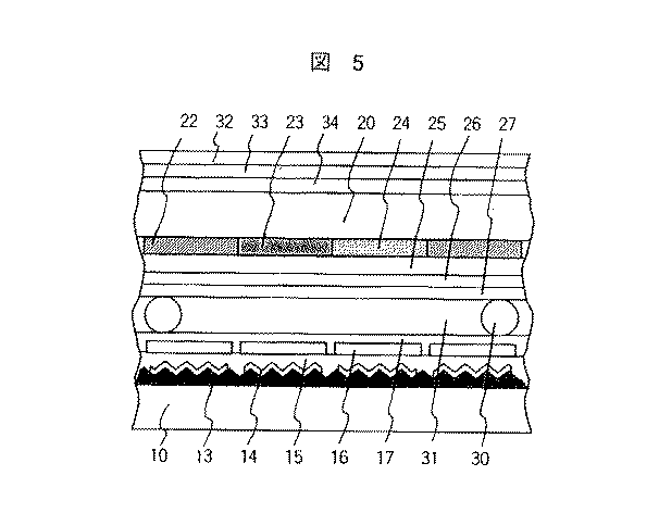
〔実施例 2〕
本発明の別の液晶表示素子の断面構造を図5に示す。同図に示すように、液晶表示素子の一方の電極基板はガラス基板10(ソーダガラス,板厚:0.7mm)上に紐状の凸部あるいは凹部からなる多数の凹凸面を有する遮光機能を付与した樹脂層13(光吸収材:黒色顔料,母材:感光性アクリル樹脂,膜厚:0.6μm,凸部または凹部の幅:13μm,凸部または凹部の高さ:1.0μm),画素部に対応する部分にのみ配置された反射膜14(アルミニウム,膜厚:100nm,サイズ:88μm×288μm),絶縁層15(アクリル系,膜厚:2.0μm),透明電極16(ITO膜,膜厚:260nm,電極数:1920本,電極ピッチ:100μm,電極幅:92μm,電極間隙:8μm),配向制御膜17(ポリイミド,膜厚:100nm)を積層して構成している。また、他方の電極基板は、ガラス基板20(ソーダガラス,板厚:0.7mm)上に赤,緑および青(シアン,マジェンタおよびイエローでも可)からなる着色層22,23,24(顔料,膜厚:1.2μm,幅:100μm),平坦化膜25(アクリル系,膜厚:2.0μm),透明電極26(ITO膜,膜厚:260nm,電極数:240本,電極ピッチ:300μm,電極幅:292μm,電極間隙:8μm),配向制御膜27(ポリイミド,膜厚:100nm)を積層して構成している。そして、この2つの電極基板をポリマービーズのスペーサ材30(粒径:6μm)を介して配置し、ガラス基板10,20の間に、液晶31(シアノPCHおよびトラン誘導体からなる液晶組成物、液晶厚み:6μm,ツイスト角:250°)を封入している。また、一方の電極基板のガラス基板20上に所定の位相板33,34および偏光板32を配置して反射型カラー液晶表示素子を構成している。
【0053】
図4は、このように構成した液晶表示素子40に液晶駆動用ICを搭載したテープ・キャリア・パッケージ41および駆動用外部回路42とを配置した反射型カラー液晶表示装置を示している。
【0054】
本実施例によれば、紐状の凸部あるいは紐状の凹部からなる微少な凹凸面を有する樹脂層13に黒色顔料等を分散させ、かつ反射膜14を短冊状にパターニングして画素電極に対応する部分にのみ配置することで反射電極基板に遮光機能を付与させることにより、対向基板には着色層23,24,25のみを配置した構造の液晶厚みが均一な反射型カラー液晶表示素子が作製できるので、明るく、高コントラストの表示が得られる反射型カラー液晶表示装置が提供できる。
【0055】
また、本実施例によれば、開口率を左右するパターニング処理をパターニング性のよい金属反射膜14と透明電極16,26のみにすることにより、高開口率の反射型カラー液晶表示素子が製作でき、明るく、高コントラストの表示が得られる反射型カラー液晶表示装置が提供できる。
【0056】
さらに、本実施例によれば、着色層22,23,24を三色同時印刷法を用いて形成することにより、低コストで反射型カラー液晶表示素子が製作でき、明るく、高コントラストの画像が得られる低コストの反射型カラー液晶表示装置が提供できる。
【0057】
〔実施例 3〕
本発明のさらに別の液晶表示素子の断面構造を図6に示す。同図に示すように、液晶表示素子の一方の電極基板は、ガラス基板10(ソーダガラス,板厚: 0.7mm)上に紐状の凸部あるいは凹部からなる多数の凹凸面を有する樹脂層13(光吸収材:黒色顔料,母材:感光性アクリル樹脂,膜厚:0.6μm,凸部または凹部の幅:13μm,凸部または凹部の高さ:1.0μm),画素部に対応する部分にのみ配置された反射膜14(アルミニウム,膜厚:100nm,サイズ:88μm×288μm),赤,緑および青(シアン,マジェンタおよびイエローでも可)からなる着色層22,23,24(顔料,膜厚:1.2μm,幅:100μm),平坦化膜25(アクリル系,膜厚:2.0μm),透明電極16(ITO膜,膜厚:260nm,電極数:240本,電極ピッチ:300μm,電極幅:292μm,電極間隙:8μm),配向制御膜27(ポリイミド,膜厚:100nm)を積層して構成している。また、他方の電極基板は、ガラス基板20(ソーダガラス,板厚:0.7mm)上に透明電極16(ITO膜,膜厚:260nm,電極数:1920本,電極ピッチ:100μm,電極幅:92μm,電極間隙:8μm),配向制御膜17(ポリイミド,膜厚:100nm)を積層して構成している。そしてこれらの電極基板を、ポリマービーズのスペーサ材30(粒径:6μm)を介して配置し、ガラス基板10,20の間に、液晶31(シアノPCHおよびトラン誘導体からなる液晶組成物,液晶厚み:6μm,ツイスト角: 250°)を封入する。また、液晶表示素子の一方の電極基板のガラス基板20上に所定の位相板33,34および偏光板32を配置して反射型カラー液晶表示素子を構成する。そして、図4に示すように、液晶表示素子40に液晶駆動用ICを搭載したテープ・キャリア・パッケージ41および駆動用外部回路42とを配置して反射型カラー液晶表示装置を構成する。
【0058】
本実施例によれば、紐状の凸部あるいは紐状の凹部からなる微少な凹凸面を有する樹脂層13に黒色顔料等を分散し、かつ反射膜14を短冊状にパターニングして画素電極に対応する部分にのみ配置することで樹脂層13に遮光層の機能を付与し、さらに前記反射膜14上に着色層22,23,24を積層することにより、反射膜14と透明電極16間に配置する絶縁層および遮光層が除去できるので、高開口率の反射型カラー液晶表示素子が製作でき、明るく、高コントラスト表示が得られる反射型カラー液晶表示装置が提供できる。
【0059】
また、本実施例によれば、一方のガラス基板に樹脂層13,反射膜14および着色層22,23,24を集約させることにより、他方のガラス基板には精細度の高い信号電極をガラス基板上に直接形成できるので、液晶表示素子の製作歩留まりを向上する効果がある。
【0060】
さらに、駆動用ICが搭載されたTCPの実装、並びに、修正も容易で、液晶素子の製作歩留まりを向上する効果もある。
【0061】
さらにまた、本実施例によれば、着色層22,23,の形成に三色同時印刷法を用いて重合せ印刷をすることにより着色層表面の段差が解消できるだけでなく、低コストで反射型カラー液晶表示素子ができ、明るく、高コントラストの画像が得られる低価格の反射型カラー液晶表示装置が提供できる。
【0062】
なお、本実施例では着色層22,23,24上に平坦化膜25を配置したが、前述した三色同時印刷法等を用いて重合せ印刷をすることにより、着色層22,23,24に平坦化機能を付与することができるので、平坦化膜25のない反射型カラー液晶表示素子が製作でき、明るく、高コントラスト表示が得られる低価格の反射型カラー液晶表示装置が提供できる。
【0063】
〔実施例 4〕
本発明のさらに別の液晶表示素子の断面構造を図7に示す。同図に示すように、液晶表示素子の電極基板は、ガラス基板10(ソーダガラス,板厚:0.7mm)上に紐状の凸部あるいは凹部からなる多数の凹凸面を有する樹脂層13(光吸収材:黒色顔料,母材:感光性アクリル樹脂,膜厚:0.6μm ,凸部または凹部の幅:13μm,凸部または凹部の高さ:1.0μm),画素部に対応する部分にのみ配置された反射膜14(銀,膜厚:100nm),遮光層35(硫化処理により黒化,ピッチ:100μm×300μm,幅:12μm),赤,緑および青(シアン,マジェンタおよびイエローでも可)からなる着色層22,23,24(顔料,膜厚:1.2μm,幅:100μm),透明電極16(ITO膜,膜厚:260nm,電極数:240本,電極ピッチ:300μm,電極幅:292μm,電極間隙:8μm),配向制御膜27(ポリイミド,膜厚:100nm)を積層して構成する。また、他方の電極基板を、ガラス基板20(ソーダガラス,板厚:0.7mm)上に透明電極16(ITO膜,膜厚:260nm,電極数:1920本,電極ピッチ:100μm,電極幅:92μm,電極間隙:8μm),配向制御膜17(ポリイミド,膜厚:100nm)を積層して構成する。そしてこれらの電極基板を、ポリマービーズのスペーサ材30(粒径:6μm)を介して配置し、ガラス基板間々隙部に、液晶31(シアノPCHおよびトラン誘導体からなる液晶組成物,液晶厚み:6μm,ツイスト角:250°)を封入する。また電極基板のガラス基板20上に所定の位相板33,34および偏光板32を配置して反射型カラー液晶表示素子を構成する。図4に示すように、液晶表示素子40に液晶駆動用ICを搭載したテープ・キャリア・パッケージ41および駆動用外部回路42とを配置し反射型カラー液晶表示装置を構成する。
【0064】
本実施例によれば、紐状の凸部あるいは紐状の凹部からなる微少な凹凸面を有する樹脂層13上に形成される反射膜14をパターニングせずに、硫化処理等により遮光部(ブラックマトリクス部)に対応する反射膜部35のみを黒化することにより、反射膜に段差を発生させずに遮光機能を付与できるので、着色層22,23,24表面が平坦な反射型カラー液晶表示素子が製作できるので、明るく、高コントラストの表示が得られる反射型カラー液晶表示装置が提供できる。
【0065】
また、本実施例によれば、反射膜をパターニングせずに、反射膜14の一部分を黒化処理によりマトリクス状遮光層35を形成するため、高開口率の反射型カラー液晶表示素子が製作でき、明るく,高コントラストの表示が得られる反射型カラー液晶表示装置が提供できる。
【0066】
さらに、本実施例によれば、一方のガラス基板に樹脂層13,反射膜14および着色層22,23,24を集約させることにより、他方のガラス基板には精細度の高い透明電極16をガラス基板上に直接形成できるので、液晶表示素子の製作歩留まりを向上する効果がある。
【0067】
さらにまた、駆動用ICが搭載されたTCPの実装、並びに、修正も容易で、液晶素子の製作歩留まりを向上する効果もある。
【0068】
なお、本実施例によれば、着色層22,23を三色同時印刷法を用いて重合せ印刷をすることにより着色層表面の段差が解消できるだけでなく、低コストで反射型カラー液晶表示素子ができるので、明るく、高コントラストの表示が得られる低価格の反射型カラー液晶表示装置が提供できる。
【0069】
〔実施例 5〕
次に、本発明の反射型液晶表示素子および反射型液晶表示装置の製法を図8の模式断面図に基づき説明する。工程(a):紐状の凹凸部が表面に形成された支持体となる高分子のベースフィルム12(ポリエチレンテレフタレート,膜厚:50μm,凹部ピッチ:およそ13μm,凹部深さ:1.0μm)上に黒色顔料が分散されたアクリル樹脂からなる樹脂層13(エポキシ系樹脂あるいはイミド系樹脂でも可、または、樹脂層は感光性あるいは非感光性いずれも可)を塗布(膜厚:1.5μm),乾燥後、樹脂層13上に保護フィルム(図示せず、ポリエチレン,膜厚:6μm)を設けた転写フィルムを用意する。
【0070】
上記転写フィルム11をガラス基板10(ソーダガラス,板厚:0.7mm)にロールラミネータ18(基板温度:100℃,ロール温度:100℃,ロール圧力:6kg/cm2,送り速度:0.5m/分)を用いて転写し、次いで本硬化(240℃/30分)を行い、高分子のベースフィルム12を剥がして多数の凹凸部を有する樹脂層13を形成する。
【0071】
工程(b):多数の凹凸部を有する樹脂層13上にアルミニウムの反射膜14(銀でも可,膜厚:100nm)を形成する。
【0072】
工程(c):前記反射膜14上に感光性樹脂19(感光性樹脂は非感光性樹脂でも可,膜厚:1.5μm)を塗布後、フォトマスク28を用いて前記感光性樹脂19に紫外線29を露光する。
【0073】
工程(d):前記感光性樹脂19および前記反射膜14を所定の現像条件で現像して、短冊状の反射膜14(アルミニウム,膜厚:100nm,サイズ:288μm×88μm,間隙:12μm)を形成し、さらに前記短冊状反射膜14上に絶縁層15(アクリル系樹脂),透明電極16(ITO膜,膜厚:260nm,電極数:640本,電極ピッチ:100μm,電極幅:88μm,電極間々隙:12μmの信号電極),配向制御膜17(ポリイミド,膜厚:700nm)を形成した一方の電極基板と
工程(e):一方他方のガラス基板(ソーダガラス,板厚:0.7mm)上に感光性樹脂の着色層22を塗布した後、感光性樹脂の着色層22にカラーフィルタ用フォトマスク28を介して紫外線29を露光する。
【0074】
工程(f):前記感光性着色樹脂層21を所定の現像条件で現像して、赤,緑および青(イエロー,シアンおよびマゼンタでも可)のいずれかの着色層22を形成する。
【0075】
工程(g):前記着色層22と同様の工程を繰り返すことにより、着色層23および24を形成する。
【0076】
工程(h):前記着色層22,23,24上に平坦化膜25(感光性樹脂あるいは非感光性樹脂でも可,膜厚:2.5μm)を形成後、透明電極26(ITO, 膜厚:260nm,電極数:240本,電極ピッチ:300μm,電極幅:288μm,電極間々隙:12μmの走査電極)、および配向制御膜27(ポリイミド,膜厚:70nm)を形成する。
【0077】
工程(i):上記(a)〜(d)により形成した一方の電極基板と、上記(e)〜(i)により形成した他方の電極基板とを、互いの透明電極16,26が対向するように配置し、液晶31の厚みに相当するポリマビーズのスペーサ材30 (粒径:6μm)を介して組合わせる。
【0078】
次いで、基板周辺に形成されたエポキシ樹脂にポリマビーズ(シリカビーズ等も使用可)が配合されたシール材で両電極基板をシールし、該電極基板間隙に液晶31(シアノPCHおよびトラン誘導体からからなる液晶組成物,屈折率異方性△n:0.133,ツイスト角:250°)封入,封止(感光性アクリル樹脂または感光性エポキシ樹脂)することにより反射型カラー液晶表示素子を作製した。
【0079】
さらに、図4に示すように、前記反射型カラー液晶表示素子40のガラス基板20上に所定の位相板33,34,偏光板32を配置して反射型カラー液晶表示素子を作製した。
【0080】
さらに、また、図4に示すように、前記反射型カラー液晶表示素子40に液晶駆動用ICを搭載したテープ・キャリア・パッケージ41や駆動用外部回路42を実装して反射型カラー液晶表示装置を作製した。
【0081】
〔実施例 6〕
次に、本発明の別の反射型液晶表示素子および反射型液晶表示装置の製法を図9の模式断面図に基づき説明する。工程(a):紐状の凹凸部が表面に形成された支持体となる高分子のレジストフィルム12(ポリエチレンテレフタレート,膜厚:50μm,凹部ピッチ:およそ13μm,凹部深さ:1.0μm)上に黒色顔料が分散されたアクリル樹脂からなる樹脂層13(エポキシ系樹脂あるいはイミド系樹脂でも可、または、樹脂層は感光性あるいは非感光性いずれも可)を塗布(膜厚:1.5μm),乾燥後、樹脂層13上に保護フィルム(図示せず、ポリエチレン,膜厚:6μm)を設けた転写フィルムを用意する。
【0082】
上記転写フィルム11をガラス基板10(ソーダガラス,板厚:0.7mm)にロールラミネータ18(基板温度:100℃,ロール温度:100℃,ロール圧力:6kg/cm2,送り速度:0.5m/分)を用いて転写し、次いで本硬化(240℃/30分)を行い、高分子のレジストフィルム12を剥がして多数の凹凸部を有する樹脂層13を形成する。
【0083】
工程(b):多数の凹凸部を有する樹脂層13上にアルミニウムの反射膜14(銀でも可,膜厚:100nm)を形成する。
【0084】
工程(c):前記反射膜14上に感光性樹脂19(感光性樹脂は非感光性樹脂でも可、膜厚:1.5μm)を塗布後、フォトマスク28を用いて前記感光性樹脂19に紫外線29を露光する。
【0085】
工程(d):前記感光性樹脂19および前記反射膜14を所定の現像条件で現像して、短冊状の反射膜14(アルミニウム,膜厚:100nm,サイズ:288μm×88μm,間隙:12μm)を形成し、さらに前記短冊状反射膜14上に絶縁層15(アクリル系樹脂),透明電極16(ITO膜,膜厚:260nm,電極数:640本,電極ピッチ:100μm,電極幅:88μm,電極間々隙:12μmの信号電極),配向制御膜17(ポリイミド,膜厚:700nm)を形成した一方の電極基板と
工程(e):一方他方のガラス基板(ソーダガラス,板厚:0.7mm)上に感光性樹脂の着色層22を塗布した後、感光性樹脂の着色層22に着色層用フォトマスク28を介して紫外線29を露光する。
【0086】
工程(f):前記感光性樹脂の遮光層21を所定の現像条件で現像して、赤,緑および青(イエロー,シアンおよびマゼンタでも可)のいずれかの着色層22を形成する。
【0087】
工程(g):前記着色層22と同様の工程を繰り返すことにより、着色層23および24を形成する。
【0088】
工程(h):前記着色層22,23,24上に平坦化膜25(感光性樹脂あるいは非感光性樹脂でも可,膜厚:2.5μm)を形成後、透明電極26(ITO,膜厚:260nm,電極数:240本,電極ピッチ:300μm,電極幅:288μm,電極間々隙:12μmの走査電極)、および配向制御膜27(ポリイミド,膜厚:70nm)を形成する。
【0089】
工程(i):上記(a)〜(d)により形成した一方の電極基板と、上記(e)〜(i)により形成した他方の電極基板とを、互いの透明電極16,26が対向するように配置し、液晶31の厚みに相当するポリマビーズのスペーサ材30 (粒径:6μm)を介して組合わせる。
【0090】
次いで、基板周辺に形成されたエポキシ樹脂にポリマビーズ(シリカビーズ等も使用可)が配合されたシール材で両電極基板をシールし、該電極基板間隙に液晶31(シアノPCHおよびトラン誘導体からからなる液晶組成物,屈折率異方性△n:0.133,ツイスト角:250°)封入,封止(感光性アクリル樹脂または感光性エポキシ樹脂)することにより反射型カラー液晶表示素子を作製した。
【0091】
さらに、図4に示すように、前記反射型カラー液晶表示素子40のガラス基板20上に所定の位相板33,34,偏光板32を配置して反射型カラー液晶表示素子を作製した。
【0092】
さらに、また、図4に示すように、前記反射型カラー液晶表示素子40に液晶駆動用ICを搭載したテープ・キャリア・パッケージ41や駆動用外部回路42を実装して反射型カラー液晶表示装置を作製した。
【0093】
なお、本実施例では紐状の凸部あるいは紐状の凹部による微小な凹凸面を有する樹脂層を低コスト化に有利な転写法により形成したが、印刷方式やフォトリソグラフィ法等で形成しても同様のものが得られる。本発明は紐状のパターンで微小な凹凸面を形成することが特徴であり、製法には限定されない。
【0094】
また、本実施例では反射膜として膜厚が100nmのアルミニウム膜,遮光膜として膜厚が100nmのクロム膜を形成したが、反射膜および遮光膜の材料等は、目的に応じて選択することができる。
【0095】
さらに、前記平坦化膜25の採用は目的に合わせて任意である。例えば、有効表示領域にのみ形成すれば、液晶駆動用ICが搭載されたTCP実装がより有利になる。
【0096】
このように、紐状の凸部および凹部からなる無秩序に配置された滑らかな凹凸反射面を有する反射板を内蔵することにより、入射する光を観察者側に集光させるための凸部および凹部を所定の領域内に最も密になるように配置することができるので、光の干渉による色付きのない、明るい画像が得られる反射型液晶表示装置が提供できる。
【0097】
また、紐状の凸部あるいは凹部が連続でかつ無秩序に配置、または紐状の凸部と凹部が交互でかつ無秩序に配置された滑らかな凹凸反射面を有する反射板を内蔵することにより、あらゆる方向から入射する光を観察者方向に集光させることができるだけでなく、正反射光成分を発生させる平坦な部分を少なくできる構造なので、光の干渉による色付きのない、明るい画像が得られる反射型液晶表示装置が提供できる。尚、平坦化を考えた場合は、紐状の凸部あるいは凹部が連続でかつ無秩序に配置した場合の方が、凸部あるいは凹部のいずれか一方の高さを考えればよいので、凸部と凹部が交互でかつ無秩序に配置した場合よりも良い。また、紐状の凸部あるいは凹部が連続でかつ無秩序に配置した場合より、凸部と凹部が交互でかつ無秩序に配置した場合の方が正反射光成分を発生させる平坦な部分が少なくなる可能性がある。
【0098】
また、各方位における紐状凸部あるいは紐状凹部の長さ成分がほぼ等しくなるように紐状凸部あるいは紐状凹部のパターンを制御することにより、あらゆる方向から入射する光を観察者方向に集光させることができる反射板が形成できるので、明るい画像が得られる低価格の反射型液晶表示装置が提供できる。
【0099】
また、各方位における紐状凸部あるいは凹部の長さ成分が異なるように紐状凸部あるいは紐状凹部のパターンを制御することにより、特定方向から入射する光を観察者方向に効率よく集光させることのできる反射板が形成できるので、明るい画像が得られる低価格の反射型液晶表示装置が提供できる。
【0100】
また、断面形状の傾斜角分布がほぼ左右対称な紐状凸部および紐状凹部を有する反射板を内蔵することにより紐状凸部および凹部のパターン形成が容易になるので、明るい画像が得られる反射型液晶表示装置が低コストで達成できる。
【0101】
また、紐状凸部あるいは紐状凹部からなる滑らかな凹凸面を有する樹脂層を黒色顔料等により着色するとともに、反射層を着色層のドットサイズに対応するように短冊状にパターニングする構造にすることにより高開口率の反射型液晶表示素子が製作できるので、明るい画像が得られる反射型カラー液晶表示装置が提供できる。
【0102】
また、反射板と着色層を同一基板上に形成することにより、他方のガラス基板に精細度の高い信号電極をガラス基板上に直接形成できるので、電極形成および液晶駆動用ICが搭載されたTCPの実装、並びに、修正が高歩留まりで行える液晶表示素子が製作できるので、高コントラストで明るい画像が得られる低コストの反射型液晶表示装置が提供できる。
【0103】
更に、遮光層に対応する部分の反射層を黒化処理等の手法で遮光機能を付与することにより、非開口部からの不要な反射光が大幅に低減できるので、高コントラストで明るい画像が得られる反射型液晶表示装置が低コストで達成できる。
【0104】
尚、本実施例ではポリマービーズのスペーサ材としているが、柱状スペーサを用いても良い。
【0105】
【発明の効果】
本発明によれば、明るく,低コストの反射型液晶表示装置を提供することができる。
【図面の簡単な説明】
【図1】紐状の凸部あるいは紐状の凹部からなる凹凸形成用フォトマスク・パターン及び拡散反射板を示す図である。
【図2】紐状の凸部あるいは紐状の凹部からなる拡散反射板の断面構造を示す図である。
【図3】実施例1の反射型カラー液晶表示素子の構成を示す模式断面図である。
【図4】本発明の反射型カラー液晶表示装置の構成を示す模式断面図である。
【図5】実施例2の反射型カラー液晶表示素子の構成を示す模式断面図である。
【図6】実施例3の反射型カラー液晶表示素子の構成を示す模式断面図である。
【図7】実施例4の反射型カラー液晶表示素子の構成を示す模式断面図である。
【図8】実施例1の反射型カラー液晶表示素子の製法を示す模式断面図である。
【図9】実施例2の反射型カラー液晶表示素子の製法を示す模式断面図である。
【符号の説明】
10,20…ガラス基板、11…拡散下地膜用転写フィルム、12…ベースフィルム、13…樹脂層、14…反射層、15…絶縁層、16,26…透明電極、17,27…配向制御膜、18…ラミネータ、19…感光性樹脂、21…遮光層、22,23,24…着色層、25…平坦化膜、28…フォトマスク、29…紫外線、30…スペーサ材、31…液晶、32…偏光板、33,34…位相板、40…反射型カラー液晶表示素子、41…テープ・キャリア・パッケージ、42…駆動用外部回路。[0001]
BACKGROUND OF THE INVENTION
The present invention relates to a liquid crystal display device, and more particularly to a liquid crystal display device having a function effective for a reflective color display.
[0002]
[Prior art]
As a conventional reflective type color liquid crystal display device, as shown in JP-A-4-243226 and JP-A-10-177106, a convex part or concave part having a circular shape and a symmetrical inclination angle distribution is used as a reflective film. There has been proposed a liquid crystal display device provided with a reflection plate formed underneath and configured to collect light incident from all directions in the direction of an observer in a liquid crystal element.
[0003]
In addition, in the prior art, a reflecting plate having a large number of concave and convex reflective surfaces in which circular convex portions or concave portions are irregularly arranged so as not to cause light interference is also disclosed.
[0004]
Further, as disclosed in Japanese Patent Laid-Open No. 10-177106, a convex portion or a concave portion having a circular shape and an asymmetric inclination angle distribution is formed under the reflecting film so as to collect incident light in a specific direction. There has also been proposed a liquid crystal display device provided with a reflective plate in a liquid crystal element.
[0005]
[Problems to be solved by the invention]
In the above prior art, circular convex portions or concave portions are irregularly arranged in a region corresponding to the pixel electrode portion to prevent coloring due to light interference, so that the circular convex portions or concave portions are closely packed. The number of convex portions or concave portions, which are reflection elements for controlling incident light, is greatly reduced as compared with the case where they are arranged, and the display is dark.
[0006]
In addition, the conventional technique condenses the reflected light in a specific direction by making the inclination angle distribution of the circular convex portion or concave portion asymmetric, so that the manufacturing process becomes complicated, and fine convex portions or concave portions are not formed. There was also a problem that shape control was difficult.
[0007]
Furthermore, the above-described conventional technique has a problem that the manufacturing process is complicated and requires many steps because the circular convex portions or concave portions are formed by photolithography.
[0008]
An object of the present invention is to solve the above-described problems and provide a reflection type liquid crystal display device including a reflection plate having better reflection characteristics and a method for manufacturing the same.
[0009]
[Means for Solving the Problems]
The present invention is a reflection type liquid crystal display device including a reflection plate having a structure in which a resin layer having projections and depressions and a reflection layer are laminated on a glass substrate, and in order to achieve the above object, 1) has a smooth curve String-like convex parts or string-like concave parts are arranged continuously and alternately 2) String-like convex parts having a smooth curve are continuously arranged 3) String-like concave parts having a smooth curve are continuously arranged A reflection type liquid crystal display device including a reflection plate in which a minute uneven surface is formed in a resin layer by being disposed in the substrate.
[0010]
Further, the reflector of the present invention has a string-like convex part or a string-like concave part in which the inclination angle distribution of the cross-sectional shape perpendicular to the length direction is substantially bilaterally symmetric, and the string-like convex part or the string-like shape in each direction. A reflection plate for a reflective liquid crystal display device, characterized in that a minute uneven surface is formed in a resin layer by arranging the recesses so that the total sum of the lengths of the recesses is substantially equal.
[0011]
Furthermore, the reflector of the present invention has a string-like convex part or a string-like concave part in which the inclination angle distribution of the cross-sectional shape in the direction perpendicular to the length direction is substantially bilaterally symmetric, and the string-like convex part or the string-like shape in each direction. A reflection plate for a reflective liquid crystal display device, wherein a minute uneven surface is formed on a resin layer by disposing the recesses so that the total sum of the lengths of the recesses is different.
[0012]
In the present invention, the resin layer, the reflective layer, the insulating layer, the transparent electrode, and the orientation control film having a minute concavo-convex surface composed of the string-like convex part or the string-like concave part are laminated on the glass substrate. The electrode substrate and the other electrode substrate in which the light shielding layer, the colored layer, the planarizing layer, the transparent electrode, and the orientation control are laminated on the other glass are arranged so that the transparent electrodes face each other through the liquid crystal. A reflective liquid crystal display device characterized by having an element structure.
[0013]
Further, the present invention provides a resin layer in which a black pigment or the like having a minute uneven surface composed of the string-like convex part or the string-like concave part is dispersed on a glass substrate, and a strip disposed only in a part corresponding to a pixel. One electrode substrate in which a reflective reflection, colored layer, planarization layer, transparent electrode, and orientation control film are laminated, and the other electrode substrate in which a transparent electrode and an orientation control film are laminated on the other glass substrate A reflection type liquid crystal display device having an element structure in which transparent electrodes are arranged to face each other with a liquid crystal interposed therebetween.
[0014]
Further, the present invention is characterized in that the concavo-convex pattern composed of the convex part or the concave part is formed by a simulation method of phase separation pattern generation by spinodal decomposition, and is used for forming the resin layer It is used for a light-shielding pattern, or a master pattern of a concavo-convex pattern formed on a transfer mold.
[0015]
Furthermore, the present invention is a numerical simulation using a spinodal decomposition pattern generation simulation method using 1) Cahn-Hilliard-Cook equation, 2) time-dependent Ginzburg-Landau equation, 3) Cell-Dyamical-System equation, etc. It is characterized by this.
[0016]
Furthermore, the light-shielding part pattern or the transmission part pattern for the photomask used for forming the reflector of the present invention is a pattern generated by spinodal decomposition simulation or a pattern obtained by image processing by taking the pattern into a computer or the like. It is characterized by being either.
[0017]
Furthermore, the present invention shows that the pattern generated by the simulation method exhibits a uniform reflection characteristic with respect to all directions or a reflection characteristic that condenses incident light in a specific direction. It is either one.
[0018]
The reflective liquid crystal display device of the present invention includes a reflective film formed on a resin layer having a smooth concavo-convex surface composed of the string-like pattern that can be arranged in a close-packed manner on one surface of a glass substrate, and its reflection A reflective electrode substrate in which an insulating layer, a plurality of transparent electrodes, and an orientation control film are laminated on the film, and a light-shielding layer, a colored layer, a planarization layer, a plurality of transparent electrodes, and orientation control on one surface of the other glass substrate A liquid crystal display element including a color filter substrate in which films are stacked and a liquid crystal sealed in a gap between the reflective electrode substrate and the color filter substrate is used.
[0019]
The method for producing a reflective liquid crystal display element of the present invention includes a step of applying a photosensitive resin on a glass substrate, a transfer mold roll or a mold plate having convex portions or concave portions that satisfy the above conditions, Forming a resin layer having a smooth concavo-convex surface comprising convex and concave portions, forming a reflective film on the resin layer, forming an insulating layer on the reflective film, on the insulating layer A reflective electrode substrate comprising a step of forming a transparent electrode, a step of forming an orientation control film on the transparent electrode,
A step of forming a light shielding layer on one surface of the other glass substrate, a step of forming a colored layer on the light shielding layer, a step of forming a planarizing layer on the colored layer, and a transparent electrode on the planarizing layer. A colored layer substrate comprising: a step of forming, a step of forming orientation control on the transparent electrode;
The method for manufacturing a liquid crystal display element according to
[0020]
Further, the manufacturing method of the reflective liquid crystal display device of the present invention includes 1) a string-like pattern having a smooth curve, 2) a string-like convex part and a concave part, wherein the convex part and the concave part are continuously arranged, or the convex part. Or a pattern in which concave portions are continuously arranged, 3) a pattern in which the sum of length components of convex portions and concave portions in each direction is substantially equal, or a pattern in which the sum of length components of convex portions and concave portions in each direction is different, A method of manufacturing a reflective liquid crystal display device having a reflective plate in which a reflective film is formed on a glass substrate on which a resin layer having a smooth concavo-convex surface formed so as to satisfy these conditions is formed, the reflective plate A photosensitive resin is applied to one surface of the glass substrate constituting the substrate, and the photosensitive resin is patterned using a transfer mold roll or a mold plate on which a pattern is formed so as to satisfy the above conditions. The step of forming a resin layer having a smooth uneven surface, the step of shaping the resin layer having the uneven surface into a smooth uneven surface by light irradiation or heat treatment, the resin layer having a smooth uneven surface Forming a reflective film thereon; forming a planarizing layer on the reflective film; forming a plurality of transparent electrodes on the planarized film; forming an alignment control film on the transparent electrode A reflective electrode substrate comprising:
Forming a light shielding layer on the other glass substrate, forming a colored layer on the light shielding film, forming a planarizing layer on the colored layer, and forming a plurality of transparent electrodes on the planarizing layer A step of combining a colored layer substrate comprising a step of forming an alignment control film on the transparent electrode such that the alignment control films face each other, and a gap between the reflective electrode substrate and the colored layer substrate The liquid crystal display element is manufactured by the process of encapsulating and sealing the liquid crystal in the part,
A step of bonding a predetermined phase plate and a polarizing plate to the other surface of the glass substrate on which the colored layer of the liquid crystal display element is formed, a tape carrier package (hereinafter, referred to as a liquid crystal driving IC mounted on the liquid crystal display element) And a drive external circuit, and a step of incorporating the liquid crystal display element into a frame, a case or the like.
[0021]
Another method of manufacturing the reflective liquid crystal display device of the present invention is a method of manufacturing a reflective liquid crystal display device having a reflective plate in which a reflective film is formed on a glass substrate on which a large number of fine convex portions or concave portions are formed. The light-shielding region or the transmission region has a substantially uniform width and a predetermined length with a smooth curve after a photosensitive resin is applied to one surface of the glass substrate constituting the reflection plate. Exposing the photosensitive resin through light shielding means that is patterned using spinodal decomposition so that the sum of the length components of the light shielding region or transmission region in each direction is substantially equal, A process of forming a resin layer having a smooth concavo-convex surface in which string-like convex portions and concave portions are continuously and alternately arranged by patterning by heat treatment after development, the concavo-convex surface Forming a reflective film on the resin layer having a step of forming a planarizing layer on the reflective layer, forming a plurality of transparent electrodes in the planarization film, and the reflective electrode substrate made of capital,
Forming a light shielding layer on the other glass substrate, forming a colored layer on the light shielding film, forming a planarizing layer on the colored layer, and forming a plurality of transparent electrodes on the planarizing layer And a step of combining the color filter substrate and the transparent electrode so that the transparent electrodes face each other, and a step of sealing and sealing liquid crystal in a gap portion between the reflective electrode substrate and the colored layer substrate. Make the device,
A step of bonding a predetermined phase plate and a polarizing plate to the other surface of the glass substrate on which the colored layer of the liquid crystal display element is formed, a tape carrier package (hereinafter, referred to as a liquid crystal driving IC mounted on the liquid crystal display element) And the external circuit for driving, and the step of incorporating the liquid crystal display element into a frame, a case or the like.
[0022]
DETAILED DESCRIPTION OF THE INVENTION
An example of a specific element configuration of a reflection type color liquid crystal display device provided with a built-in diffuse reflection plate having a novel pattern according to the present invention is as follows.
[0023]
(1) A string-like convex part and concave part pattern is generated by a spinodal decomposition simulation. Here, the spinodal decomposition model equations for simulating spinodal decomposition include the Cahn-Hilliard (-Cook) equation given by
[0024]
[Expression 1]
[Expression 2]
Also, a pattern simulating spinodal decomposition can be generated by numerical simulation of a spinodal decomposition model (near the enlarged Moore) by Cell-Dynamical System (CDS) shown in Equation 3.
[0027]
[Equation 3]
By using either of these, 1) Consists of string-like convex and concave patterns having a substantially uniform line width and a smooth curve. 2) String-like convex parts or concave parts are arranged continuously or alternately. 3) The inclination angle distribution of the cross-sectional shape in the direction perpendicular to the length direction of the string-like convex part and the concave part is substantially bilaterally symmetric. 4) The total sum of the lengths of the convex part and the concave part is almost equal in each direction. Or 5) A large number of smooth concavo-convex patterns satisfying conditions such as the sum of the lengths of the convex portions and the concave portions being different in each direction can be formed.
[0029]
A pattern composed of such string-like convex portions or concave portions is applied to a photosensitive resin (film thickness: 0.5 to 2.5 μm) applied on a glass substrate using a transfer roll or plate or the like. Light (wavelength: 365 nm, light quantity: 50 to 500 mj / cm) on a resin pattern formed by a transfer roll (roll speed: 0.1 to 3 m / min) or a plate 2 ), Heat (50 to 150 ° C.) and pressure (1 to 12 kg / cm) 2 ) And patterning the photosensitive resin, or using a simulation method for pattern generation by spinodal decomposition on a photosensitive resin (film thickness: 0.5 to 2.5 μm) applied on a glass substrate. Exposure through a photomask using the prepared string-like pattern as a light-shielding pattern or transmission pattern (wavelength: 365 nm, light quantity: 50 to 500 mj / cm 2 A predetermined development and curing to pattern the photosensitive resin (width: 5 to 20 μm, height or depth: 0.5 to 2.0 μm),
(2) forming a reflective film (a thin film of aluminum, aluminum alloy, silver, silver alloy, etc., film thickness: 100 to 300 nm) on the patterned resin layer;
(3) forming an insulating layer (acrylic photosensitive resin or non-photosensitive resin, film thickness: 1.0 to 3.0 μm) on the reflective film;
(4) A transparent electrode is formed on the insulating layer (ITO (Indium Tin Oxide), film thickness: 100 to 300 nm) and patterned (number of electrodes: 1920, pitch: 100 μm, gap between electrodes: 8 to 20 μm). Process,
(5) One electrode substrate comprising a step of forming an orientation control film (polyimide, film thickness: 50 to 100 nm, temperature: 230 to 250 ° C.) on the transparent electrode;
On glass substrate
(6) a step of forming a light-shielding layer (a low-surface reflective light-shielding film such as a black pigment-dispersed photosensitive resin or three-layer chromium; film thickness: 0.1 to 1.2 μm, pitch: 100 μm, width: 10 to 25 μm);
(7) A colored layer (red, green, blue or cyan, magenta, yellow, pigment dispersed acrylic photosensitive resin, film thickness: 0.5 to 1.5 μm, pitch: 100 μm, width: 75 on the light shielding layer. ~ 90 μm),
(8) A step of forming a planarizing film (acrylic photosensitive resin, film thickness: 1.0 to 3.0 μm, curing temperature: 230 to 250 ° C./1 hour) on the colored layer,
(9) A transparent electrode is formed on the planarizing film (ITO (Indium Tin Oxide), film thickness: 100 to 300 nm), patterning (number of electrodes: 240, pitch: 300 μm, gap between electrodes: 8 to 20 μm) The process of
(10) Another electrode substrate comprising a step of forming an orientation control film (polyimide, film thickness: 50 to 150 nm, curing temperature: 230 to 250 ° C.) on the transparent electrode,
(11) A spacer material (polymer beads, silica beads, glass fiber, particle size: 6 μm) is combined so that the alignment control film surfaces face each other, and the periphery of both electrode substrates is sealed (the spacer in the epoxy resin). Bonding and sealing with dispersed materials)
(12) A liquid crystal display element is formed by a step of sealing and sealing liquid crystal between both electrode substrates.
[0030]
And
(13) A step of bonding a predetermined phase plate and a polarizing plate to the glass substrate on which the reflection plate of the liquid crystal display element is not formed,
(14) connecting a tape carrier package (hereinafter referred to as TCP) in which a liquid crystal driving IC is mounted on the liquid crystal display element and an external driving circuit;
(15) a step of incorporating the liquid crystal display element into a frame, a case, or the like;
Thus, the liquid crystal display device of the present invention is completed.
[0031]
According to the present invention, the string-like convex part and the concave part for reflecting as much light incident from any direction or light incident from a specific direction as possible to the viewer side are provided in the part corresponding to the pixel electrode. Since a reflective plate having a smooth concavo-convex surface arranged so that the string-like convex part or the string-like concave part is the densest is incorporated, a reflective liquid crystal display device with a bright display can be provided.
[0032]
Further, according to the present invention, it is known as a phase separation phenomenon of a polymer block polymer or the like as an original pattern of a transfer roll, a plate, a photomask or the like that forms a string-like concavo-convex pattern composed of the convex portions and concave portions. Bright display with an irregular array pattern and a pattern in which string-like convex parts or string-like concave parts can be arranged most densely because it uses a phase separation generation pattern obtained by a computer simulation method for analyzing spinodal decomposition A low-cost reflective liquid crystal display device can be provided.
[0033]
Furthermore, according to the present invention, a string-like pattern that can be arbitrarily controlled by computer simulation is used as a mold or photomask pattern of the transfer roll or plate, and without changing the cross-sectional shape of the convex and concave portions, By controlling the arrangement ratio of the length component of the string-like convex part or concave part in the azimuth direction, it is possible to easily control reflection characteristics such as condensing reflected light in a specific direction, and a reflective liquid crystal display having desired reflection characteristics Devices and reflectors can be provided.
[0034]
Furthermore, the phase separation generation pattern obtained by computer simulation is taken into a computer, and image processing is performed to correct the pattern. This makes it easy to obtain the most suitable photomask and transfer mold for forming methods such as the transfer method or photolithography method. Therefore, not only the incident light from any direction can be collected on the viewer side, but also the specular reflection light component (light component reflected from the flat area) that degrades the image is small, and more It is possible to provide a reflective liquid crystal display device and a reflector that can provide a bright display.
[0035]
Next, a reflective liquid crystal display device suitable for implementing the present invention will be described. In the present invention, a 1/2 VGA compatible hand having a display scale of 640 × 240 dots (pixel pitch: 0.3 mm × 0.3 mm, pixel size: 0.288 mm × 0.288 mm, screen diagonal size: 8.1 inches) Reflective super twisted nematic color liquid crystal display devices (hereinafter referred to as reflective STN color liquid crystal display devices) used for outdoor applications, such as hold type personal computers (hereinafter referred to as hand held PCs) explain.
[0036]
However, since the present invention does not depend on the liquid crystal driving method, either the active addressing method or the passive method can be applied, and the present invention is not limited to the STN liquid crystal display method.
[0037]
[Example]
[Example 1]
The reflection type liquid crystal display device of the present invention is such that a string-like concavo-convex pattern is formed on the resin layer that is the base layer of the diffusive reflector so that a bright image without coloring due to light interference can be obtained. is there.
[0038]
FIG. 1A shows a photomask pattern for forming a string-like uneven pattern on a resin layer as an underlayer of a diffuse reflector, where a black part (light-shielding part) becomes a convex part or a concave part. is there. However, depending on the material of the resin layer to be used, it is necessary to invert the black portion and the white portion in the same pattern. FIG. 1B shows a resin layer generated with the photomask pattern of FIG.
[0039]
FIG. 2 shows a resin layer on which the string-like uneven pattern shown in FIG.
It is cut by a2 and a part of the cross section is shown. 2A shows a pattern in which string-like convex portions and string-like concave portions are alternately and continuously arranged, and FIG. 2B shows a pattern in which string-like convex portions are continuously arranged. FIG. 2C shows a pattern in which string-like concave portions are continuously arranged. Here, d0, d1, and d2 are the lengths of the convex portions or the concave portions, and h indicates the height of the convex portions or the depth of the concave portions. d1 shows the length of the part where the pattern of the convex part or the concave part and a1-a2 intersect at right angles, and this corresponds to the width of the string-like convex part and concave part. That is, FIG. 2 (b) means a pattern in which convex or concave shapes that draw a parabola of length d1 and height h are continuously arranged. Depending on the material, there are cases where the entire width cannot be made completely constant, but the effect of the present invention can be obtained if the width is almost constant.
[0040]
The characteristics of the string-like convex pattern, concave pattern or concave-convex pattern formed on the resin layer of the present invention will be described.
[0041]
Since the incident light reflects the shape of the convex or concave portions of the string-like pattern, the intensity distribution of the reflected light is symmetric with respect to the substrate normal when the tilt angle distribution draws a parabola that is substantially symmetric. . Therefore, if left and right non-objects are used, the light intensity distribution can be made non-left and right objects, and the light intensity distribution can have directionality.
[0042]
Further, the total sum of the light intensity distributions shown in FIG. 1B depends on the lengths of the convex portions or concave portions, d0, d1, and d2 shown in FIG. Therefore, when the sum total of the length of the convex part or recessed part of the horizontal direction (b1 direction) shown in FIG.1 (b) and the length of the convex part or recessed part of the vertical direction (direction b2) are the same. The sum of the light intensity distributions in the horizontal and vertical directions is equal. That is, the brightness in the vertical direction is the same as that in the horizontal direction. Further, when the sum of the lengths of the protrusions or recesses in the vertical direction (b2 direction) is longer than the sum of the lengths of the protrusions or recesses in the horizontal direction (direction b1), the light intensity in the horizontal direction The sum of the distributions is larger than the sum of the light intensity distributions in the vertical direction. That is, the horizontal direction is brighter than the vertical direction. Similarly, in the oblique direction (direction of b3, b4), the brightness can be made the same or changed depending on the length of the convex portion or the concave portion. Also, the lines shown in FIG. 2 are the recesses and recesses, the projections and projections, and the boundaries between the recesses and projections. Accordingly, if the vertical and horizontal ratios of the number of boundaries are the same, the brightness in the vertical direction and the horizontal direction are equal.
[0043]
Moreover, if the convex part and concave part of a string-like pattern extend linearly (parallel) in the same direction, the brightness is reduced by light interference. Therefore, the convex portions and concave portions of the string-like pattern shown in FIG. 1B are configured to extend in a curved line. That is, the interference of light is reduced by reducing the number of the straight portions where the convex portions and the concave portions are parallel. Most desirable is a configuration in which each convex portion and concave portion draw a curve and extend in a random direction (disorder). In this case, light interference is minimized.
[0044]
Further, as shown in FIGS. 2A, 2B, and 2C, the convex portions and the concave portions are arranged adjacent to each other so that the convex portions and the concave portions continue continuously. In addition, a flat portion between the convex portion and the convex portion and between the concave portion and the concave portion can be eliminated. Thereby, not only the flat part which becomes the specular reflection light which is an unnecessary light component can be eliminated, but also the incident light can be efficiently condensed in the direction of the observer, so that a bright reflector can be obtained. In addition, when a convex part or a recessed part is comprised continuously so that there may be no flat part, since a convex part or a recessed part will be arrange | positioned most densely, such a state is hereafter called the closest packing arrangement | positioning.
[0045]
In this embodiment, the length d corresponding to the width of the string-like convex part or string-like concave part is in the range of 5 to 20 μm, more preferably in the range of 8 to 15 μm, and the height of the string-like convex part or string-like concave part and The depth h is in the range of 0.5 to 2.0 μm, more preferably in the range of 0.8 to 1.5 μm.
[0046]
Next, FIG. 3 and FIG. 4 show a cross-sectional structure of an embodiment of the liquid crystal display element and the liquid crystal display device used in the reflective liquid crystal display device of the present invention. FIG. 3 shows a cross-sectional structure of the liquid crystal display element, and FIG. 4 shows a cross-sectional structure of the liquid crystal display device. As shown in FIG. 3, one of the electrode substrates of the liquid crystal display element has a number of concavo-convex surfaces consisting of string-like convex portions or string-like concave portions on a glass substrate 10 (soda glass, plate thickness: 0.7 mm). Resin layer 13 (acrylic, film thickness: 1.5 μm, convex or concave width: 13 μm, convex or concave height: 1.0 μm), reflective film 14 (aluminum, film thickness: 100 nm), insulating layer 15 (acrylic, film thickness: 2.0 μm), transparent electrode 16 (ITO film, film thickness: 260 nm, number of electrodes: 1920, electrode pitch: 100 μm, electrode width: 88 μm, electrode gap: 12 μm), orientation control film 17 (polyimide, film thickness: 100 nm) is laminated. The other electrode substrate is a light shielding layer 21 (three-layer chrome, film thickness: 0.1 μm, width: 12 μm, pigment black, film thickness: 0.0 mm) on a glass substrate 20 (soda glass, plate thickness: 0.7 mm). 6 μm, width: 12 μm), colored layers 22, 23, 24 (pigment type, film thickness: 1.2 μm, width: 100 μm), planarization film 25 (acrylic, film thickness: 2.0 μm), transparent electrode 26 ( ITO film, film thickness: 260 nm, number of electrodes: 240, electrode pitch: 300 μm, electrode width: 288 μm, electrode gap: 12 μm), and orientation control film 27 (polyimide, film thickness: 100 nm) are laminated. . These electrode substrates are arranged via polymer bead spacer material 30 (particle size: 6 μm), and a liquid crystal 31 (a liquid crystal composition comprising cyano PCH and a tolan derivative, liquid crystal thickness: between the
[0047]
According to the present embodiment, the string-like convex part or the string-like concave part is formed by making the reflecting element for condensing light incident from all directions in the direction of the observer into the string-like convex part or the string-like concave part. Since a reflective color liquid crystal display element can be manufactured that has a disordered and close-packed reflective plate in the region corresponding to the pixel portion, a reflective color liquid crystal display device capable of obtaining a bright display without light interference is provided. Can be provided.
[0048]
In addition, according to this example, a spinodal known as a phase separation phenomenon such as a polymer block copolymer is used to form a photomask pattern or transfer pattern for forming a minute uneven pattern consisting of a string-like convex part or a string-like concave part. By using a computer simulation method to analyze the decomposition, the arrangement of the string-like projections or string-like depressions can be controlled arbitrarily, so that a reflective color liquid crystal display element suitable for the lighting environment can be manufactured, and light interference There can be provided a reflective color liquid crystal display device which can provide a brighter display.
[0049]
Further, according to the present embodiment, the string-like convex portion is formed by a transfer method such as a transfer film in which a resin layer having a minute uneven surface composed of a string-like concave portion is laminated on a transfer roll, a transfer plate, or a base film. Alternatively, a reflective color liquid crystal display element can be manufactured at a low cost by forming a resin layer having a minute concavo-convex surface composed of string-like concave portions, and thus a low-cost reflective color liquid crystal display device can be provided.
[0050]
In addition, although it is common in the following examples, in the present invention, a string-like convex part or a string-like concave pattern was produced using a computer simulation method for analyzing spinodal decomposition. Patterns may be directly produced by controlling environmental conditions such as temperature and pressure of liquid crystals and colloids and inducing phenomena such as phase transition or phase separation.
[0051]
In this embodiment, the width of the string-like convex portion or the string-like concave portion is 13 μm, but the present invention is not limited to this width. Further, in this embodiment, the width of the string-like convex part or the string-like concave part is 13 μm, but the present invention may be constituted by a plurality of string-like convex parts or string-like concave parts having different widths. This is also common in the following embodiments. By configuring with different widths as described above, the intensity distribution with respect to the angle can be changed, and a bright display can be achieved over a wide range.
[0052]
Example 2
FIG. 5 shows a cross-sectional structure of another liquid crystal display element of the present invention. As shown in the figure, one electrode substrate of the liquid crystal display element has a light-shielding function having a large number of concave and convex surfaces made of string-like convex portions or concave portions on a glass substrate 10 (soda glass, plate thickness: 0.7 mm). Applied resin layer 13 (light absorbing material: black pigment, base material: photosensitive acrylic resin, film thickness: 0.6 μm, width of convex part or concave part: 13 μm, height of convex part or concave part: 1.0 μm), Reflective film 14 (aluminum, film thickness: 100 nm, size: 88 μm × 288 μm), insulating layer 15 (acrylic, film thickness: 2.0 μm), transparent electrode 16 (ITO film) disposed only in the portion corresponding to the pixel portion , Film thickness: 260 nm, number of electrodes: 1920, electrode pitch: 100 μm, electrode width: 92 μm, electrode gap: 8 μm), and orientation control film 17 (polyimide, film thickness: 100 nm). The other electrode substrate is a
[0053]
FIG. 4 shows a reflective color liquid crystal display device in which a
[0054]
According to this embodiment, a black pigment or the like is dispersed in the
[0055]
Further, according to the present embodiment, a reflective color liquid crystal display element having a high aperture ratio can be manufactured by using only the metal
[0056]
Furthermore, according to the present embodiment, by forming the
[0057]
[Example 3]
A cross-sectional structure of still another liquid crystal display element of the present invention is shown in FIG. As shown in the figure, one electrode substrate of the liquid crystal display element is a resin layer having a number of concavo-convex surfaces composed of string-like convex portions or concave portions on a glass substrate 10 (soda glass, plate thickness: 0.7 mm). 13 (light absorbing material: black pigment, base material: photosensitive acrylic resin, film thickness: 0.6 μm, width of protrusion or recess: 13 μm, height of protrusion or recess: 1.0 μm), corresponding to pixel portion Reflective film 14 (aluminum, film thickness: 100 nm, size: 88 μm × 288 μm), colored layers 22, 23, 24 (pigments made of red, green and blue (can be cyan, magenta and yellow)) , Film thickness: 1.2 μm, width: 100 μm), planarization film 25 (acrylic, film thickness: 2.0 μm), transparent electrode 16 (ITO film, film thickness: 260 nm, number of electrodes: 240, electrode pitch: 300 μm, electrode width: 292 μm, electricity Gap: 8 [mu] m), the alignment control film 27 (polyimide thickness: are formed by stacking a 100 nm). The other electrode substrate is a transparent electrode 16 (ITO film, film thickness: 260 nm, number of electrodes: 1920, electrode pitch: 100 μm, electrode width on a glass substrate 20 (soda glass, plate thickness: 0.7 mm). 92 μm, electrode gap: 8 μm) and an orientation control film 17 (polyimide, film thickness: 100 nm) are laminated. These electrode substrates are arranged via polymer bead spacer material 30 (particle diameter: 6 μm), and liquid crystal 31 (liquid crystal composition comprising cyano PCH and a tolan derivative, liquid crystal thickness is interposed between
[0058]
According to this embodiment, a black pigment or the like is dispersed in the
[0059]
In addition, according to the present embodiment, the
[0060]
Further, the mounting and correction of the TCP on which the driving IC is mounted is easy, and there is an effect of improving the production yield of the liquid crystal element.
[0061]
Furthermore, according to the present embodiment, not only the step of the colored layer surface can be eliminated by superposition printing using the three-color simultaneous printing method for forming the
[0062]
In this embodiment, the
[0063]
[Example 4]
FIG. 7 shows a cross-sectional structure of still another liquid crystal display element of the present invention. As shown in the figure, the electrode substrate of the liquid crystal display element is a
[0064]
According to the present embodiment, the light-shielding portion (black) is formed by sulfidation or the like without patterning the
[0065]
Further, according to this embodiment, since the matrix light shielding layer 35 is formed by blackening a part of the
[0066]
Furthermore, according to the present embodiment, the
[0067]
Furthermore, the mounting and correction of the TCP on which the driving IC is mounted can be easily performed, and the manufacturing yield of the liquid crystal element can be improved.
[0068]
According to this embodiment, the
[0069]
[Example 5]
Next, a manufacturing method of the reflective liquid crystal display element and the reflective liquid crystal display device of the present invention will be described based on the schematic cross-sectional view of FIG. Step (a): On a polymer base film 12 (polyethylene terephthalate, film thickness: 50 μm, recess pitch: approximately 13 μm, recess depth: 1.0 μm) serving as a support having a string-like uneven portion formed on the surface
[0070]
The transfer film 11 is placed on a glass substrate 10 (soda glass, plate thickness: 0.7 mm) and a roll laminator 18 (substrate temperature: 100 ° C., roll temperature: 100 ° C., roll pressure: 6 kg / cm). 2 , Feed speed: 0.5 m / min), followed by main curing (240 ° C./30 min), peeling the
[0071]
Step (b): An aluminum reflective film 14 (silver can be used, film thickness: 100 nm) is formed on the
[0072]
Step (c): Photosensitive resin 19 (photosensitive resin may be non-photosensitive resin, film thickness: 1.5 μm) is applied on the
[0073]
Step (d): The
Step (e): A photosensitive resin
[0074]
Step (f): The photosensitive
[0075]
Step (g): Colored layers 23 and 24 are formed by repeating the same steps as those for the
[0076]
Step (h): After forming a flattening film 25 (photosensitive resin or non-photosensitive resin, film thickness: 2.5 μm) on the
[0077]
Step (i): The
[0078]
Next, both electrode substrates are sealed with a sealing material in which polymer beads (silica beads or the like can be used) are blended with an epoxy resin formed around the substrate, and liquid crystal 31 (consisting of cyano PCH and a tolan derivative is provided in the gap between the electrode substrates. A reflective color liquid crystal display element was produced by enclosing and sealing (photosensitive acrylic resin or photosensitive epoxy resin) with a liquid crystal composition, refractive index anisotropy Δn: 0.133, twist angle: 250 °.
[0079]
Furthermore, as shown in FIG. 4,
[0080]
Further, as shown in FIG. 4, the reflective color liquid crystal display device is mounted with a
[0081]
[Example 6]
Next, another manufacturing method of the reflective liquid crystal display element and the reflective liquid crystal display device of the present invention will be described based on the schematic cross-sectional view of FIG. Step (a): On a polymer resist film 12 (polyethylene terephthalate, film thickness: 50 μm, recess pitch: approximately 13 μm, recess depth: 1.0 μm) serving as a support having a string-like uneven portion formed on the surface
[0082]
The transfer film 11 is placed on a glass substrate 10 (soda glass, plate thickness: 0.7 mm) and a roll laminator 18 (substrate temperature: 100 ° C., roll temperature: 100 ° C., roll pressure: 6 kg / cm). 2 , Feed rate: 0.5 m / min), followed by main curing (240 ° C./30 min), peeling the polymer resist
[0083]
Step (b): An aluminum reflective film 14 (silver can be used, film thickness: 100 nm) is formed on the
[0084]
Step (c): Photosensitive resin 19 (photosensitive resin may be non-photosensitive resin, film thickness: 1.5 μm) is applied on the
[0085]
Step (d): The
Step (e): After coating the photosensitive resin
[0086]
Step (f): The light-
[0087]
Step (g): Colored layers 23 and 24 are formed by repeating the same steps as those for the
[0088]
Step (h): After forming a flattened film 25 (photosensitive resin or non-photosensitive resin, thickness: 2.5 μm) on the
[0089]
Step (i): The
[0090]
Next, both electrode substrates are sealed with a sealing material in which polymer beads (silica beads or the like can be used) are blended with an epoxy resin formed around the substrate, and liquid crystal 31 (consisting of cyano PCH and a tolan derivative is provided in the gap between the electrode substrates. A reflective color liquid crystal display element was produced by enclosing and sealing (photosensitive acrylic resin or photosensitive epoxy resin) with a liquid crystal composition, refractive index anisotropy Δn: 0.133, twist angle: 250 °.
[0091]
Furthermore, as shown in FIG. 4,
[0092]
Further, as shown in FIG. 4, the reflective color liquid crystal display device is mounted with a
[0093]
In this embodiment, the resin layer having a minute uneven surface by the string-like convex part or the string-like concave part is formed by a transfer method advantageous for cost reduction, but it is formed by a printing method, a photolithography method, or the like. The same can be obtained. The present invention is characterized by forming a minute uneven surface with a string-like pattern, and is not limited to the manufacturing method.
[0094]
In this embodiment, an aluminum film having a film thickness of 100 nm is formed as the reflection film, and a chromium film having a film thickness of 100 nm is formed as the light shielding film. However, materials of the reflection film and the light shielding film can be selected according to the purpose. it can.
[0095]
Further, the use of the
[0096]
Thus, the convex part and recessed part for condensing incident light to an observer side by incorporating the reflecting plate which has the smooth uneven | corrugated reflective surface arrange | positioned randomly which consists of a string-like convex part and a recessed part Can be arranged so as to be the most dense within a predetermined region, so that it is possible to provide a reflective liquid crystal display device capable of obtaining a bright image without coloring due to light interference.
[0097]
In addition, by incorporating a reflective plate having a smooth concavo-convex reflective surface in which string-like convex portions or concave portions are arranged continuously and randomly, or string-like convex portions and concave portions are alternately and randomly arranged, Reflective type that not only collects light incident from the direction toward the viewer but also reduces the number of flat parts that generate specularly reflected light components. A liquid crystal display device can be provided. When flattening is considered, it is only necessary to consider the height of either the convex portion or the concave portion when the string-like convex portions or concave portions are arranged continuously and disorderly. It is better than the case where the concave portions are arranged alternately and randomly. In addition, it is possible to reduce the number of flat parts that generate specularly reflected light components when the convex and concave portions are arranged alternately and randomly rather than when the string-like convex or concave portions are arranged continuously and randomly. There is sex.
[0098]
In addition, by controlling the pattern of the string-like convex part or the string-like concave part so that the length components of the string-like convex part or the string-like concave part in each azimuth are almost equal, the light incident from all directions is directed to the observer direction. Since a reflecting plate that can be condensed can be formed, a low-cost reflective liquid crystal display device that can obtain a bright image can be provided.
[0099]
In addition, by controlling the pattern of the string-like convex part or the string-like concave part so that the length component of the string-like convex part or the concave part in each direction is different, the light incident from a specific direction is efficiently condensed in the observer direction. Therefore, it is possible to provide a low-cost reflective liquid crystal display device capable of obtaining a bright image.
[0100]
In addition, by incorporating a reflector having a string-like convex part and a string-like concave part whose cross-sectional inclination angle distribution is substantially symmetrical, pattern formation of the string-like convex part and the concave part is facilitated, and a bright image can be obtained. A reflective liquid crystal display device can be achieved at low cost.
[0101]
In addition, the resin layer having a smooth concavo-convex surface composed of string-like convex portions or string-like concave portions is colored with a black pigment or the like, and the reflective layer is patterned in a strip shape so as to correspond to the dot size of the colored layer. As a result, a reflective liquid crystal display element having a high aperture ratio can be manufactured, so that a reflective color liquid crystal display device capable of obtaining a bright image can be provided.
[0102]
In addition, by forming the reflector and the colored layer on the same substrate, a high-definition signal electrode can be directly formed on the other glass substrate. Since a liquid crystal display element that can be mounted and corrected at a high yield can be manufactured, a low-cost reflective liquid crystal display device that can obtain a bright image with high contrast can be provided.
[0103]
Furthermore, by adding a light-shielding function to the reflective layer corresponding to the light-shielding layer using a technique such as blackening, unnecessary reflected light from the non-opening can be greatly reduced, resulting in a bright image with high contrast. The reflection type liquid crystal display device can be achieved at low cost.
[0104]
In this embodiment, the spacer material of polymer beads is used, but a columnar spacer may be used.
[0105]
【The invention's effect】
According to the present invention, a bright and low-cost reflective liquid crystal display device can be provided.
[Brief description of the drawings]
FIG. 1 is a view showing a photomask pattern for forming concavities and convexities and a diffusive reflecting plate composed of cord-like convex portions or cord-like concave portions.
FIG. 2 is a diagram showing a cross-sectional structure of a diffuse reflector including a string-like convex part or a string-like concave part.
3 is a schematic cross-sectional view showing a configuration of a reflective color liquid crystal display element of Example 1. FIG.
FIG. 4 is a schematic cross-sectional view showing a configuration of a reflective color liquid crystal display device of the present invention.
5 is a schematic cross-sectional view showing a configuration of a reflective color liquid crystal display element of Example 2. FIG.
6 is a schematic cross-sectional view showing a configuration of a reflective color liquid crystal display element of Example 3. FIG.
7 is a schematic cross-sectional view showing a configuration of a reflective color liquid crystal display element of Example 4. FIG.
8 is a schematic cross-sectional view showing a method for producing the reflective color liquid crystal display element of Example 1. FIG.
9 is a schematic cross-sectional view showing a method for producing the reflective color liquid crystal display element of Example 2. FIG.
[Explanation of symbols]
DESCRIPTION OF
Claims (4)
前記樹脂層は、高分子ブロック共重合体の相分離現象により得られる相分離生成パターンを用いて形成された紐状の凹凸パターンを有する反射型液晶表示装置。Resin layer on a glass substrate, a reflective layer, an insulating layer, a first substrate is laminated a transparent electrode and an alignment control layer in this order, the light-shielding layer and the colored layer on a glass substrate, a planarization layer, a transparent electrode, an orientation control A reflective liquid crystal display device comprising: a second substrate in which layers are sequentially stacked ; and a liquid crystal sandwiched between the first substrate and the second substrate,
The reflection type liquid crystal display device, wherein the resin layer has a string-like concavo-convex pattern formed using a phase separation generation pattern obtained by a phase separation phenomenon of a polymer block copolymer .
前記樹脂層の紐状の凹凸パターンの断面形状は、凸部と凹部が交互に連続して配置された形状である反射型液晶表示装置。 The reflective liquid crystal display device according to claim 1,
The cross-sectional shape of the string-like uneven pattern of the resin layer is a reflective liquid crystal display device in which convex portions and concave portions are alternately arranged continuously .
前記樹脂層の紐状の凹凸パターンの平面形状は、凸部と凹部が曲線を描き、ランダムな方向に伸びて形成された形状である反射型液晶表示装置。 The reflective liquid crystal display device according to claim 1 or 2,
The reflective liquid crystal display device, wherein the planar shape of the string-like concavo-convex pattern of the resin layer is a shape in which convex portions and concave portions are curved and extended in random directions .
前記樹脂層は、黒色に着色された反射型液晶表示装置。 The reflective liquid crystal display device according to any one of claims 1 to 3,
The resin layer is a reflective liquid crystal display device colored in black .
Priority Applications (5)
| Application Number | Priority Date | Filing Date | Title |
|---|---|---|---|
| JP13537899A JP3671740B2 (en) | 1999-05-17 | 1999-05-17 | Reflective liquid crystal display |
| TW088117709A TW538279B (en) | 1998-10-23 | 1999-10-13 | A reflective color liquid crystal display apparatus |
| US09/425,614 US6476890B1 (en) | 1998-10-23 | 1999-10-22 | Reflective color liquid crystal display apparatus with colored polymer layer |
| KR1019990045960A KR100708926B1 (en) | 1998-10-23 | 1999-10-22 | A reflective color liquid crystal display apparatus |
| US10/219,291 US6803980B2 (en) | 1998-10-23 | 2002-08-16 | Reflective color liquid crystal display apparatus |
Applications Claiming Priority (1)
| Application Number | Priority Date | Filing Date | Title |
|---|---|---|---|
| JP13537899A JP3671740B2 (en) | 1999-05-17 | 1999-05-17 | Reflective liquid crystal display |
Publications (2)
| Publication Number | Publication Date |
|---|---|
| JP2000321568A JP2000321568A (en) | 2000-11-24 |
| JP3671740B2 true JP3671740B2 (en) | 2005-07-13 |
Family
ID=15150321
Family Applications (1)
| Application Number | Title | Priority Date | Filing Date |
|---|---|---|---|
| JP13537899A Expired - Fee Related JP3671740B2 (en) | 1998-10-23 | 1999-05-17 | Reflective liquid crystal display |
Country Status (1)
| Country | Link |
|---|---|
| JP (1) | JP3671740B2 (en) |
Families Citing this family (8)
| Publication number | Priority date | Publication date | Assignee | Title |
|---|---|---|---|---|
| EP1231487A4 (en) * | 1999-10-21 | 2003-06-04 | Matsushita Electric Ind Co Ltd | Reflecting plate, method for manufacturing the same, display element, and display device |
| JP3559505B2 (en) | 2000-07-24 | 2004-09-02 | ダイセル化学工業株式会社 | Transmission type light scattering sheet |
| WO2002010806A1 (en) * | 2000-07-28 | 2002-02-07 | Matsushita Electric Industrial Co., Ltd. | Reflection sheet and production method therefor, and display unit using it |
| JP4658346B2 (en) * | 2001-01-31 | 2011-03-23 | 京セラ株式会社 | Reflector and liquid crystal display device |
| TW200424676A (en) * | 2003-05-14 | 2004-11-16 | Prime View Int Corp Ltd | Reflector plate structure of LCD and manufacturing method thereof |
| JP2005266206A (en) * | 2004-03-18 | 2005-09-29 | Hitachi Chem Co Ltd | Liquid crystal display device |
| JP4970502B2 (en) * | 2009-07-13 | 2012-07-11 | シャープ株式会社 | Reflective liquid crystal display |
| EP3094160A4 (en) * | 2014-01-10 | 2017-08-30 | JX Nippon Oil & Energy Corporation | Optical substrate, mold to be used in optical substrate manufacture, and light emitting element including optical substrate |
-
1999
- 1999-05-17 JP JP13537899A patent/JP3671740B2/en not_active Expired - Fee Related
Also Published As
| Publication number | Publication date |
|---|---|
| JP2000321568A (en) | 2000-11-24 |
Similar Documents
| Publication | Publication Date | Title |
|---|---|---|
| KR100708926B1 (en) | A reflective color liquid crystal display apparatus | |
| US6888678B2 (en) | Irregular-shape body, reflection sheet and reflection-type liquid crystal display element, and production method and production device therefor | |
| US6130736A (en) | Liquid crystal display with corrugated reflective surface | |
| JP4059512B2 (en) | Transflective liquid crystal display device | |
| JP2000047200A (en) | Diffusive reflector, liquid crystal display device using that, and its production | |
| JP3753673B2 (en) | Manufacturing method of liquid crystal display device | |
| JP3733923B2 (en) | Mask and display device manufacturing method | |
| TW200403492A (en) | Mask, substrate with light reflecting film, method for forming light reflecting film, method for manufacturing electro-optical device, electro-optical device, and electronic apparatus | |
| JP3671740B2 (en) | Reflective liquid crystal display | |
| JP3649075B2 (en) | Liquid crystal display | |
| TW200402574A (en) | Mask, substrate with light reflective film, method for manufacturing light reflective film, liquid crystal display device, and electronic apparatus | |
| JPH11237625A (en) | Photomask and production of rugged body using the phtomask | |
| US6919943B2 (en) | Substrate for a liquid crystal device, method of manufacturing a substrate for a liquid crystal device, a liquid crystal device, a method of manufacturing a liquid crystal device, and an electronic apparatus | |
| JP2003215574A (en) | Reflective liquid crystal display | |
| JP4055453B2 (en) | Manufacturing method of color filter for transflective color liquid crystal display device | |
| JP2000131685A (en) | Reflection type color liquid crystal display device | |
| JP2002214590A (en) | Reflective liquid crystal display | |
| WO2020124705A1 (en) | Preparation method for display panel, display panel, and display device | |
| JP3566874B2 (en) | Manufacturing method of liquid crystal display device | |
| JP4007101B2 (en) | Reflective liquid crystal display | |
| JP2000267086A (en) | Manufacture of electrode substrate for reflective liquid crystal display device and electrode substrate for reflective liquid crystal display device using the same | |
| JP2001188112A (en) | Reflecting plate and its manufacturing method, and element and device for display | |
| JP2001194661A (en) | Reflective liquid crystal display device | |
| JP2003156766A (en) | Reflection type liquid crystal display unit and its manufacturing method | |
| JPH1114982A (en) | Reflection type liquid crystal display device |
Legal Events
| Date | Code | Title | Description |
|---|---|---|---|
| A977 | Report on retrieval |
Free format text: JAPANESE INTERMEDIATE CODE: A971007 Effective date: 20041101 |
|
| A131 | Notification of reasons for refusal |
Free format text: JAPANESE INTERMEDIATE CODE: A131 Effective date: 20041109 |
|
| A521 | Written amendment |
Free format text: JAPANESE INTERMEDIATE CODE: A523 Effective date: 20050111 |
|
| TRDD | Decision of grant or rejection written | ||
| A01 | Written decision to grant a patent or to grant a registration (utility model) |
Free format text: JAPANESE INTERMEDIATE CODE: A01 Effective date: 20050329 |
|
| A61 | First payment of annual fees (during grant procedure) |
Free format text: JAPANESE INTERMEDIATE CODE: A61 Effective date: 20050411 |
|
| FPAY | Renewal fee payment (event date is renewal date of database) |
Free format text: PAYMENT UNTIL: 20090428 Year of fee payment: 4 |
|
| FPAY | Renewal fee payment (event date is renewal date of database) |
Free format text: PAYMENT UNTIL: 20090428 Year of fee payment: 4 |
|
| FPAY | Renewal fee payment (event date is renewal date of database) |
Free format text: PAYMENT UNTIL: 20100428 Year of fee payment: 5 |
|
| FPAY | Renewal fee payment (event date is renewal date of database) |
Free format text: PAYMENT UNTIL: 20110428 Year of fee payment: 6 |
|
| FPAY | Renewal fee payment (event date is renewal date of database) |
Free format text: PAYMENT UNTIL: 20110428 Year of fee payment: 6 |
|
| S531 | Written request for registration of change of domicile |
Free format text: JAPANESE INTERMEDIATE CODE: R313531 |
|
| FPAY | Renewal fee payment (event date is renewal date of database) |
Free format text: PAYMENT UNTIL: 20110428 Year of fee payment: 6 |
|
| R371 | Transfer withdrawn |
Free format text: JAPANESE INTERMEDIATE CODE: R371 |
|
| FPAY | Renewal fee payment (event date is renewal date of database) |
Free format text: PAYMENT UNTIL: 20110428 Year of fee payment: 6 |
|
| S111 | Request for change of ownership or part of ownership |
Free format text: JAPANESE INTERMEDIATE CODE: R313111 |
|
| S631 | Written request for registration of reclamation of domicile |
Free format text: JAPANESE INTERMEDIATE CODE: R313631 |
|
| FPAY | Renewal fee payment (event date is renewal date of database) |
Free format text: PAYMENT UNTIL: 20110428 Year of fee payment: 6 |
|
| R350 | Written notification of registration of transfer |
Free format text: JAPANESE INTERMEDIATE CODE: R350 |
|
| FPAY | Renewal fee payment (event date is renewal date of database) |
Free format text: PAYMENT UNTIL: 20120428 Year of fee payment: 7 |
|
| S111 | Request for change of ownership or part of ownership |
Free format text: JAPANESE INTERMEDIATE CODE: R313121 Free format text: JAPANESE INTERMEDIATE CODE: R313115 |
|
| FPAY | Renewal fee payment (event date is renewal date of database) |
Free format text: PAYMENT UNTIL: 20120428 Year of fee payment: 7 |
|
| R350 | Written notification of registration of transfer |
Free format text: JAPANESE INTERMEDIATE CODE: R350 |
|
| FPAY | Renewal fee payment (event date is renewal date of database) |
Free format text: PAYMENT UNTIL: 20120428 Year of fee payment: 7 |
|
| FPAY | Renewal fee payment (event date is renewal date of database) |
Free format text: PAYMENT UNTIL: 20130428 Year of fee payment: 8 |
|
| FPAY | Renewal fee payment (event date is renewal date of database) |
Free format text: PAYMENT UNTIL: 20130428 Year of fee payment: 8 |
|
| FPAY | Renewal fee payment (event date is renewal date of database) |
Free format text: PAYMENT UNTIL: 20140428 Year of fee payment: 9 |
|
| R250 | Receipt of annual fees |
Free format text: JAPANESE INTERMEDIATE CODE: R250 |
|
| R250 | Receipt of annual fees |
Free format text: JAPANESE INTERMEDIATE CODE: R250 |
|
| R250 | Receipt of annual fees |
Free format text: JAPANESE INTERMEDIATE CODE: R250 |
|
| R250 | Receipt of annual fees |
Free format text: JAPANESE INTERMEDIATE CODE: R250 |
|
| LAPS | Cancellation because of no payment of annual fees |