JP3671448B2 - Image signal processing device - Google Patents
Image signal processing device Download PDFInfo
- Publication number
- JP3671448B2 JP3671448B2 JP02290795A JP2290795A JP3671448B2 JP 3671448 B2 JP3671448 B2 JP 3671448B2 JP 02290795 A JP02290795 A JP 02290795A JP 2290795 A JP2290795 A JP 2290795A JP 3671448 B2 JP3671448 B2 JP 3671448B2
- Authority
- JP
- Japan
- Prior art keywords
- line
- data signal
- signal
- memory
- output
- Prior art date
- Legal status (The legal status is an assumption and is not a legal conclusion. Google has not performed a legal analysis and makes no representation as to the accuracy of the status listed.)
- Expired - Fee Related
Links
Images


Description
【0001】
【産業上の利用分野】
本発明は、ビデオカメラ等において動画データや静止画データを生成する画像信号処理装置に関する。
【0002】
【従来の技術】
マルチメディアの普及に伴い、動画データや静止画データをコンピュータやワークステーション等に取り込むためのインタフェースとして、デジタルスチルカメラが注目されている。多量の画像を取り込むときなどには、スチルカメラは、従来から使用されているスキャナに比べて即時性や経済性に優れ、また、小型軽量化が可能であるので手軽に使用できるという利点がある。この経緯については、テレビジョン学会誌Vol.46、No.7(1992)第827頁〜828頁において論じられている。
【0003】
デジタルスチルカメラを実現するために使用する撮像素子としては、汎用性や従来のビデオカメラの技術を応用できる等の点から、現在のビデオカメラで一般的に使用されている画素混合方式の撮像素子を用いるのが望ましい。また、画素混合方式の撮像素子を用いた場合は、その読み出し方式を変更することにより、動画撮影に加えて静止画撮影にも使用することができる利点がある。次に、その説明を行なう。
【0004】
画素混合方式の撮像素子を用いた動画撮影では、フィールド蓄積読み出しを行なう。フィールド蓄積読み出しは、画素混合方式のCCD撮像素子において上下2画素のデータを素子内で混合して読み出すもので、その代表的なフィルタ配列を図2に示している。最初のフィールドにおいては、図2に示すように、水平走査毎に上下ラインが加算されて、A1,A2の順番で信号が順次読み出される。また、次のフィールドにおいては、同様に、水平走査毎に上下ラインが加算されて、B1,B2の順番で順次読み出される。この結果、センサーからは、水平走査毎に、(Mg+Ye),(G+Cy)と(G+Ye),(Mg+Cy)が交互に出力される。ここで、Wr=Mg+Ye,Gb=G+Cy,Gr=G+Ye,Wb=Mg+Cyとすれば、撮像素子からのデータ信号は、現データ信号をSL、1ライン遅延したデータ信号をSL-1、2ライン遅延したデータ信号をSL-2として、図3に示すように表わされる。
【0005】
画素混合方式の撮像素子を用いた静止画記録には、画素混合された各フィールドの出力データ信号をインターリーブして1フレームの画像を記録するフレームスチル画記録方式と、1フィールドの画像のみを記録するフィールドスチル画記録方式とがある。フィールドスチル画記録方式の場合には、
(1)特開平1−143482号公報に記載されているようなマトリクス補正ができなくなり垂直色モアレが増加する。
(2)垂直方向の解像度が不足し、静止画としては十分な画質が得られない。
という問題がある。従って、静止画記録にはフレームスチル画記録方式が望ましいが、フレームスチル画記録方式の場合、移動量の大きい被写体ではブレが生じて2重像となる問題点がある。
【0006】
このような問題を解決するため、図4に示すように、最初のフィールドにおいては、水平走査毎に1ラインずつ撮像素子内で画素データを混合せずにデータ信号を読み出し、また次のフィールドにおいても同様に、水平走査毎に1ラインずつデータ信号を読み出して静止画記録を行なう方式が開発されている。このように読み出されたデータ信号は、図5に示すようになる。この方式によれば、ブレが無く解像度が劣化しない静止画を得ることが可能となる。この読み出し方法をフレーム蓄積読み出し方法と呼び、この静止画記録方式をフルフレームスチル画記録方式と名付ける。この詳細は、特開平4−274036号公報及び特開平4−331393号公報に述べられている。以下、その方法について述べる。
【0007】
画素混合方式の撮像素子から画素混合をしないでデータ信号を読み出すことは、この撮像素子の駆動パルスを制御することで実現できる。そして、フルフレームスチル画記録方式を実現するためには、撮像素子上に配列されたフィルタ配置の順に画像データ信号を1H(ライン)ずつ順次読み出すことが必要がある。しかしながら、撮像素子からは、1枚のフレーム画を構成する画像データが、1ラインおきに1フィールドずつ出力されるので、このままでは信号処理を行なうことができない。そこで検討を行なった結果、撮像素子から出力される2フィールド(1フレーム)分の画像データを蓄積可能なフレームメモリを用い、撮像素子から出力されるデータ信号の1フレーム分をフレームメモリに記憶した後に該メモリーからノンインタレース読み出しを行えば、フルフレームスチル画記録が可能になるという結論に達した。そして画像シミュレーションによる検討の結果では、画素混合方式の撮像素子を用いたフルフレームスチル画記録でも、スチル画としては十分な画質の記録が得られることがわかった。
【0008】
撮像素子からフィールド蓄積読み出しを行なって動画処理を行なうときには、色信号及び輝度信号を、共に、現データ信号,1ライン遅延データ信号,2ライン遅延データ信号の3ライン分のデータ信号から生成する。また、フレーム蓄積読み出しを行なって静止画処理を行なうときには、色信号に関しては、1ライン遅延データ信号,2ライン遅延データ信号,3ライン遅延データ信号の3ライン分のデータ信号から生成し、輝度信号は、現データ信号,1ライン遅延データ信号,2ライン遅延データ信号,3ライン遅延データ信号,4ライン遅延データ信号の5ライン分のデータ信号から生成する。図6は、この様子を示している。
【0009】
このような画像信号処理を行なうためには、ビデオカメラ及びその他の映像機器には、画像データ信号の遅延信号を生成するための遅延回路が不可欠であることがわかる。
【0010】
【発明が解決しようとする課題】
従来のデジタル信号処理では、遅延回路としてメモリを用いている。しかし、全信号処理回路を1つのICに1チップ化しようとするときには、チップ面積や消費電力に占める前記メモリの比重が大きくなる。静止画信号処理を行なうときには現データ信号〜4ライン遅延データ信号を生成するための4H(ライン)分のラインメモリが必要となるが、これらのラインメモリをICに内蔵しようとすると該ICのチップ面積の増加や消費電力が増大するといった問題が発生する。
【0011】
従って、本発明の目的は、画像データ信号を遅延するために使用するメモリを少なくすることができる画像信号処理装置を提供することにある。
【0012】
【課題を解決するための手段】
本発明は、この目的を達成するために、1画面分のデータを記憶するフレームメモリと、1画面を水平方向にn分割して各ブロック毎にデータを読み出すようにフレームメモリを制御するメモリコントロール部と、フレームメモリから読み出された1ライン分((1/n)H分)のデータを記憶する第1の(1/n)Hラインメモリと、第1のラインメモリから出力されるデータ信号を記憶する第2の(1/n)Hラインメモリと、第2のラインメモリから出力されるデータ信号を記憶する第3の(1/n)Hラインメモリと、以下第(m−1)のラインメモリから出力されるデータ信号を記憶する第mの(1/n)Hラインメモリと、これらのメモリを制御するメモリコントロール部を設けたことにある。
【0013】
【作用】
画素混合方式の撮像素子で静止画を撮影する場合、その出力データ信号はフィールド単位となる。データ信号は、フレームメモリにノンインタレースで記憶した後に読み出しを行ない処理をする。静止画の場合は動画と違ってリアルタイムの処理が要求されないため、画面を水平方向に分割して処理することが可能となる。以下、水平方向に2分割して画像処理をする場合の手順を説明する。
【0014】
(1)フレームメモリに書き込んだデータを、(1/2)H分づつ左半画面分を読み出して処理を行なう。
【0015】
(2)左半画面分の処理データを再びフレームメモリに書き込む。
【0016】
(3)残り右半画面分のデータを読み出し処理を行なう。
【0017】
(4)右半画面分の処理データを再びフレームメモリに書き込む。
【0018】
この方式により静止画処理を行なう場合は、1ライン分のデータを遅延させるには(1/2)H分の容量のメモリですむ。そのため、4ライン分の遅延データ信号を、
(1/2)H×4=2H分
の容量のメモリで生成できる。動画処理の場合には従来どおり2H分の容量のメモリを用いたリアルタイム処理となるため、2H分のメモリにより動画及び静止画の両方の処理が可能となる。
【0019】
なお、一枚の画面を左半画面と右半画面とに分けて処理をする場合、完全に左半分と右半分とで独立した信号処理を行なえば、左右の画面の境目で不連続部分が生じ画面上で歪となる。これは信号処理で水平方向のフィルタ処理を行なっているためであり、この不連続が生じないようにするために次のような工夫を行なう。
【0020】
撮像素子からフレームメモリにデータを書き込む際には、あらかじめ数画素分のオフセットを水平方向のアドレスにもたせて書き込むようにする。次に左半画面分の処理結果を再びフレームメモリに書き込む際にはアドレス0から書き始めるようにすれば、水平方向に数画素分の上書きされないデータが残る。そうすれば、右半面分の処理をする際に、水平方向のフィルタ処理が左画面から右画面に連続して行なうことができ、画面中央部で歪を生じることなくフレーム静止画を得ることができる。
【0021】
以上、デジタルカメラの信号処理について、現データ信号〜4ライン遅延データ信号までを2H分の容量のラインメモリで生成する信号遅延処理を述べたが、フレームメモリを用いて静止画処理を行なう場合は、水平分割数を増やすことによりより多くの遅延データ信号が得られる。
【0022】
ここで、フレームメモリと1H分のラインメモリから現データ信号〜mライン遅延データ信号を生成する方法につき説明する。フレームメモリに記憶した1画面分のデータを遅延回路に出力するとき、1画面を水平方向にn等分したブロック毎にデータを読みだす。読み出したデータは第1の(1/n)Hラインメモリに記憶し、1ライン遅延データ信号を生成する。次に第1のラインメモリから出力されるデータ信号を第2の(1/n)Hラインメモリに記憶することにより2ライン遅延データ信号を生成し、以下同様に、第mの(1/n)Hラインメモリによりmライン遅延データ信号を生成することができる。
【0023】
このようにすれば、1ライン分の遅延データ信号を生成するのに(1/n)H分の容量のメモリで足りるので、現データ信号〜mライン遅延データ信号を(1/n)H×m=(m/n)Hの容量のメモリで生成でき、垂直方向のフィルタリング等で多数のラインを使用するときなどにメモリの量を軽減できる。また、動画のリアルタイム処理を行なう場合には(m/n)Hのラインメモリとして使用することができる。
【0024】
【実施例】
以下、本発明の実施例を図面を参照して説明する。
【0025】
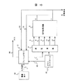
図1は、本発明になる画像信号処理装置のブロック図である。この画像信号処理装置は、フレームメモリと(1/n)H分の容量のラインメモリをm個用いて現データ信号〜mライン遅延データ信号を生成する回路構成のものである。ここで、Hは、水平方向1ライン分の画像データ(画素)数である。
【0026】
図1において、1は入力データ信号、2はフレームメモリ、3は前記フレームメモリ3から出力されるデータ信号、4は信号遅延回路、5は前記信号遅延回路4から出力される現データ信号、6は同1ライン遅延データ信号、7は同2ライン遅延データ信号、8は同nライン遅延データ信号、9は信号処理回路、10は前記信号処理回路9で処理して出力されたデータ信号、82は前記フレームメモリ2のアドレス信号、83は前記アドレス82を発生するメモリコントロール部である。
【0027】
フレームメモリ2は、1フレーム分の入力データ信号1を記憶する。フレームメモリ2に記憶した画像データ信号は、メモリコントロール部83により制御されるアドレス信号82により、画面を水平方向にn等分して区分した各ブロック毎に読み出される。読み出された画像データ信号は、水平方向の長さが(1/n)Hとなるので、(1/n)Hの容量のメモリで1ライン遅延データ信号を生成することができる。信号遅延回路4は、フレームメモリ2から読み出したデータ信号3から現データ信号5,1ライン遅延データ信号6,2ライン遅延データ信号7…mライン遅延データ信号8までのデータ信号を生成し、信号処理回路9に出力する。
【0028】
信号処理回路9は、信号遅延回路4で生成した現データ信号5〜mライン遅延データ信号8を処理した処理結果を出力データ信号10として出力する。出力データ信号10は、再びフレームメモリ2の前記読み出したデータ上に書き込むか、または、他の記憶装置に出力される。このような処理を1画面にわたりn回繰り返すことで、処理された1画面分の画像データ信号をフレームメモリ2に得ることができる。フレームメモリ2に記憶した画像データ信号(処理結果)は、外部出力データ信号94として外部に出力される。
【0029】
ここで、フレームメモリ2からのデータ読み出し方法について、図7を参照して説明する。同図において、2はフレームメモリ、11はフレームメモリ内の画像データ信号をn等分したうちの最初の1ブロック、12は次の1ブロック、13は最後の1ブロック、3は該フレームメモリ2から読み出されるデータ信号である。
【0030】
フレームメモリ2に記憶された1画面分の画像データは、図7に示すように、水平方向にn等分した状態で、メモリコントロール部83により制御されたアドレス信号82により、最初の1ブロック11から読み出される。読み出したデータ信号3は、信号遅延回路4に送られる。信号遅延回路4で生成した現データ信号5〜mライン遅延データ信号8に対しては信号処理回路9で所定の信号処理を行ない、処理した結果を再びフレームメモリ2のブロック11に上書きする。次に、ブロック12のデータを同様に読み出し、処理した結果をブロック12に上書きする。この処理を最後のブロック13まで繰り返せば、1フレーム全体の画像データに対する処理が完了し、この処理結果がフレームメモリ2に記憶されることになる。
【0031】
次に、前記信号遅延回路4による現データ信号5〜mライン遅延データ信号8の生成について、図8を参照して説明する。同図において、1は入力データ信号、2はフレームメモリ、3は前記フレームメモリ2から出力されるデータ信号、4は信号遅延回路、14は1ライン遅延データ信号を生成するための(1/n)Hの容量をもつラインメモリ、6は前記ラインメモリ14により生成した1ライン遅延データ信号、15は2ライン遅延データ信号を生成するための(1/n)Hの容量をもつラインメモリ、6は前記ラインメモリ15により生成した2ライン遅延データ信号、16はmライン遅延データ信号を生成するための(1/n)Hの容量をもつラインメモリ、8は前記ラインメモリ16により生成したmライン遅延データ信号、82は前記フレームメモリ2に対するアドレス信号、83は前記アドレス信号82を発生するメモリコントロール部である。
【0032】
フレームメモリ2からは、図7に示すように、画面を水平方向にn等分して区分した各ブロック毎にデータを読み出す。これはメモリコントロール部83によりフレームメモリ2のアドレス信号82を制御して行なう。読み出したデータは、水平方向の長さが(1/n)Hであるので、(1/n)Hの容量のラインメモリで1ライン(H/nライン長)分の遅延データ信号を生成できる。信号遅延回路4では、フレームメモリ2から読み出したデータ信号3を現データ信号5として出力すると共に(1/n)Hラインメモリ14に記憶する。次の1ライン(H/nライン長)分のデータ信号3がフレームメモリ2から入力されると、(1/n)Hラインメモリ14からは1ライン遅延データ信号6が出力され、同データ信号6が(1/n)Hラインメモリ15に記憶される。以下、同様の遅延処理を行なってnライン目のデータ信号が信号遅延回路4に入力したとき、(1/n)Hラインメモリ16からmライン遅延データ信号8が出力される。このように、フレームメモリ2内部のデータを水平方向にn分割して各ブロック毎に処理すれば、1H分のメモリ容量で現データ信号5〜mライン遅延データ信号8を生成することができ、遅延データ信号生成のためのラインメモリの容量を軽減することができる。
【0033】
次に、前記信号遅延回路4によりリアルタイムで1ライン遅延データ信号を生成するための遅延処理について、図9を参照して説明する。同図において、1は入力データ信号、4は信号遅延回路、14,15…16は(1/n)Hの容量をもつラインメモリ、17は1ライン遅延データ信号である。
【0034】
信号遅延回路4に入力される入力データ信号1のうちの最初の(1/n)H分がラインメモリ14に記憶される。次に新たな(1/n)H分のデータ信号1が入力されると、ラインメモリ14の内容(記憶データ)が押し出されて後段のラインメモリ15に記憶(移動)され、新たに入力した入力データ信号1は前段のラインメモリ14に記憶される。以下同様に、更に新たなデータが前段のラインメモリ14に入力されると、ラインメモリ14,15に記憶されているデータは、順次に後段のラインメモリに記憶(移動)されていき、m/nH分のデータ信号が入力されたときには、信号遅延回路4内部のラインメモリ14〜16がデータ信号で満ちてリアルタイムで1ライン遅延データ信号17が生成される。
【0035】
図10は、本発明になる画像信号処理装置を使用したビデオカメラ等においてフレーム静止画を生成,記録するときの信号処理方式を示している。同図において、18は画素混合方式の撮像素子、2はデータ信号を1フレーム分記憶するためのフレームメモリ、82は前記フレームメモリ2のアドレス信号、83は前記アドレス信号82を生成するメモリコントロール部、3は前記フレームメモリ2から読み出した0.5H分のデータ信号、4は現データ信号〜4ライン遅延データ信号を生成するための信号遅延回路、5は前記信号遅延回路4で生成した現データ信号、6は同1ライン遅延データ信号、7は同2ライン遅延データ信号、19は同3ライン遅延データ信号、20は同4ライン遅延データ信号、9は色信号及び輝度信号を生成するための信号処理回路、21は前記信号処理回路9で生成した色信号、22は同輝度信号である。
【0036】
画素混合方式の撮像素子18からフレーム読み出しにより得た入力データ信号1は、1フレーム分をフレームメモリ2に書き込む。このとき、水平方向のアドレスには数画素分のオフセットをもたせて書き込むようにする。これは、画面中央部の処理を連続した状態で行なえるようにするためである。次に、メモリコントロール部83によりフレームメモリ2へのアドレス信号82を制御して、このフレームメモリ2から左半画面分のデータ(1水平走査あたり0.5H分)を順次に読み出して信号遅延回路4に入力する。信号遅延回路4に入力したデータ信号3は、図11に示す遅延方式で遅延することにより、現データ信号5,1ライン遅延データ信号6,2ライン遅延データ信号7、3ライン遅延データ信号19、4ライン遅延データ信号20を生成する。遅延回路4で生成した現データ信号5〜4ライン遅延データ信号20は、信号処理回路9に送り、色信号21及び輝度信号22を生成する。生成した色信号21及び輝度信号22は、外部の記憶装置に出力されるか、もしくはフレームメモリ2の左半画面分の領域にアドレス0から書き込む。右半画面についても同様の処理を行なえば、2ライン分の容量のメモリで現データ信号〜4ライン遅延データ信号を用いた静止画処理を行なうことができ、高精細のフルフレーム静止画をフレームメモリ2に得ることができる。フレームメモリ2からは外部に画像データ信号94を出力する。
【0037】
図11は、本発明になる画像信号処理装置を使用したデジタルスチルカメラの静止画処理における回路構成を示している。同図において、1は入力データ信号、2はフレームメモリ、3は前記フレームメモリ2から読み出されるデータ信号、5は現データ信号、23は1ライン遅延データ信号生成用ラインメモリ、6は1ライン遅延データ信号、24は2ライン遅延データ信号生成用ラインメモリ、7は2ライン遅延データ信号、25は3ライン遅延データ信号生成用ラインメモリ、19は3ライン遅延データ信号、26は4ライン遅延データ信号生成用ラインメモリ、20は4ライン遅延データ信号、27は各ラインメモリ23〜26に供給するアドレス信号、4は現データ信号〜4ライン遅延データ信号を生成する前記信号遅延回路である。
【0038】
入力されるデータ信号1は、一旦、フレームメモリ2に1画面分記憶する。このとき、水平方向のアドレスには数画素分のオフセットをもたせて書き込むようにする。次に、フレームメモリ2からデータをノンインタレースで左半画面分(0.5H分)だけ読み出して信号遅延回路4に入力する。
【0039】
信号遅延回路4は、入力したデータ信号3を0.5H分の容量の1ライン遅延データ信号生成用ラインメモリ23に送り、1ライン遅延データ信号6を生成する。以下同様に、2ライン遅延データ信号生成用メモリ24,3ライン遅延データ信号生成用メモリ25,4ライン遅延データ信号生成用メモリ26で、それぞれ、2ライン遅延データ信号7,3ライン遅延データ信号19,4ライン遅延データ信号20を生成し、後段の信号処理回路9に送る。
【0040】
図12は、本発明になる画像信号処理装置における前記静止画処理の際に各ラインメモリ23〜26にデータを書き込む場合のアドレス信号及び書き込み信号のタイミングを示している。同図において、28は信号遅延回路4の入力データ信号(3)、27は各ラインメモリ23〜26のアドレス信号、29はラインメモリ23の書き込み信号、30はラインメモリ24の書き込み信号、31はラインメモリ25の書き込み信号、32はラインメモリ26の書き込み信号、33はラインメモリ23に記憶したデータ、34はラインメモリ24に記憶したデータ、35はラインメモリ25に記憶したデータ、36はラインメモリ26に記憶したデータである。なお、各ラインメモリ23〜26は、図11における各ラインメモリ23〜26に対応する。
【0041】
入力データ信号28及びアドレス信号27は、同じ周期でラインメモリ23に入力する。入力データ信号28は、書き込み信号29によってラインメモリ23におけるアドレス信号27の番地に書き込む。また、ラインメモリ23から出力されるデータ信号は、書き込み信号30によってラインメモリ24におけるアドレス信号27の番地に書き込む。以下同様に、書き込み信号31と書き込み信号32により、ラインメモリ24,25からの出力データをそれぞれラインメモリ25,26に書き込む。
【0042】
図13は、本発明になる画像信号処理装置における前記静止画処理の際に各ラインメモリ23〜26からデータを読み出す場合のアドレス信号及び読み出し信号のタイミングを示している。同図において、27は各ラインメモリ23〜27のアドレス信号、37はラインメモリ23の読み出し信号、38はラインメモリ24の読み出し信号、39はラインメモリ25の読み出し信号、40はラインメモリ26の読み出し信号、41はラインメモリ23から読み出される読み出しデータ信号、42はラインメモリ24から読み出される読み出しデータ信号、43はラインメモリ25から読み出される読み出しデータ信号、44はラインメモリ26から読み出される読み出しデータ信号、45は各ラインメモリ23〜26から読み出される各読み出しデータ信号の位相を揃えるための同期信号、46は読み出しデータ信号41を同期信号45と同相にした出力データ信号、47は読み出しデータ信号42を同期信号45と同相にした出力データ信号、48は読み出しデータ信号43を同期信号45と同相にした出力データ信号、49は読み出しデータ信号44を同期信号45と同相にした出力データ信号を表わしている。なお、各ラインメモリ23〜26は、図11の各ラインメモリ23〜26に対応している。
【0043】
アドレス信号27及びメモリ読み出し信号37は同じ周期でラインメモリ23に入力する。ラインメモリ23に記憶されているデータは、アドレス信号27の番地から読み出し信号37により該ラインメモリ23の読み出しデータ信号41として読み出される。以下同様に、読み出し信号38,読み出し信号39,読み出し信号40により各ラインメモリ24〜26のデータを読み出してデータ信号42〜44を出力する。読み出した各読み出しデータ信号41〜44は、同期信号45により同期化してそれぞれ出力データ信号46〜49とし、該信号遅延回路4から出力する。
【0044】
図14は、本発明になる画像信号処理装置による動画処理のための遅延処理回路構成を示している。同図において、4は信号遅延回路、3はこの信号遅延回路4の入力データ信号、23,24は1ライン遅延データ信号生成用ラインメモリ、50,51は2系統のデータ信号を同時化するための選択器、53は1ライン遅延データ信号、25,26は2ライン遅延データ信号生成用ラインメモリ、54は2ライン遅延データ信号、27は各ラインメモリ23〜26にデータを書き込み、または読み出すためのアドレス信号、52は2系統のデータ信号を同時化するために前記選択器50,51を切り換える切り換え信号である。
【0045】
信号遅延回路4に入力した1H分のデータ信号3は、0.5H分をラインメモリ23に記憶し、残りの0.5H分をラインメモリ24に記憶する。次の1H分の処理では、ラインメモリ23から出力されるデータ信号をラインメモリ25に記憶し、ラインメモリ24から出力されるデータ信号をラインメモリ26に記憶する。
【0046】
また、ラインメモリ23,24から出力されたデータ信号は、選択器50で同時化して1ライン遅延データ信号53を生成する。そして、ラインメモリ25,26から出力されたデータ信号は、選択器51で同時化して2ライン遅延データ信号54を生成する。
【0047】
図15は、本発明になる画像信号処理装置による前記動画処理の際にラインメモリ23〜26にデータを書き込む場合のアドレス信号と書き込み信号のタイミングを示している。同図において、55は入力データ信号(3)、27は各ラインメモリ23〜26に供給するアドレス信号、29はラインメモリ23に対する書き込み信号、30はラインメモリ24に対する書き込み信号、31はラインメモリ25に対する書き込み信号、32はラインメモリ26に対する書き込み信号、56はラインメモリ23に記憶された0.5H分のデータ信号、57はラインメモリ24に記憶された0.5H分のデータ信号、58はラインメモリ25に記憶された0.5H分のデータ信号、59はラインメモリ26に記憶された0.5H分のデータ信号である。なお、各ラインメモリ23〜26は、図14の各ラインメモリ23〜26に対応する。
【0048】
撮像素子からサンプリング周波数fs(周期1/fs)で読み出された入力データ信号55は、その2倍の周期(2/fs)のアドレス信号27でラインメモリ23,24に書き込まれる。
【0049】
ラインメモリ23に対する書き込み信号29は、入力データ信号55の奇数番目のデータ信号(図中でD11,D13,D15…)に同期した形で該ラインメモリ23に入力する。その結果、図に示すように、ラインメモリ23のアドレス0にはデータ信号D11が、アドレス1にはデータ信号D13が、アドレス2にはデータ信号D15がそれぞれ書き込まれることになる。
【0050】
ラインメモリ24に対する書き込み信号30は、入力データ信号55の偶数番目の信号(図中でD12,D14,D16…)に同期した形で該ラインメモリ24に入力する。その結果、図に示すように、ラインメモリ24のアドレス0にはデータ信号D12が、アドレス1にはデータ信号D14が、アドレス2には信号D16がそれぞれ書き込まれることになる。このように、0.5Hの容量をもつ2つのラインメモリ23,24に対して1ライン目の1H分のデータ信号を記憶する。2ライン目の1H分のデータ信号55が入力されたときは、入力した2ライン目のデータ信号55は、ラインメモリ23,24にそれぞれ0.5H分記憶される。そして、ラインメモリ23から出力される1ライン目の0.5H分のデータ信号はラインメモリ25に、ラインメモリ24から出力される残りの0.5H分のデータ信号はメモリ6にそれぞれ記憶される。
【0051】
図16は、本発明になる画像信号処理装置による前記動画処理の際にラインメモリ23〜26からデータを読み出す場合のアドレス信号と読み出し信号のタイミングを示している。同図において、27はラインメモリ23〜26からデータを読み出す際のアドレスを示すアドレス信号、37はラインメモリ23からデータを読み出すための読み出し信号、38はラインメモリ24からデータを読み出すための読み出し信号、39はラインメモリ25からデータを読み出すための読み出し信号、40はラインメモリ26からデータを読み出すための読み出し信号、60はラインメモリ23から読み出した読み出しデータ信号、61はラインメモリ24から読み出した読み出しデータ信号、62はラインメモリ25から読み出した読み出しデータ信号、63はラインメモリ26から読み出した読み出しデータ信号、45は、ラインメモリ23,24からの読み出しデータ信号60,61の位相を揃え、ラインメモリ25からの読み出しデータ信号62,63の位相を揃えるための同期信号、64は読み出しデータ信号60を同期信号45と同相にした読み出しデータ信号、65は読み出しデータ信号61を同期信号45と同相にした読み出しデータ信号、66は読み出しデータ信号62を同期信号45と同相にした読み出しデータ信号、67は読み出しデータ信号63を同期信号45と同相にした読み出しデータ信号である。なお、各ラインメモリ23〜26は、図14の各ラインメモリ23〜26に対応する。
【0052】
アドレス信号27とラインメモリ23に対する読み出し信号37,ラインメモリ24に対する読み出し信号38,ラインメモリ25に対する読み出し信号39及びラインメモリ25に対する読み出し信号40は、メモリにデータを書き込むときと同じ周期(2/fs)で、各ラインメモリ23〜26に入力される。ラインメモリ23では、入力したアドレス信号27の番地に記憶しているデータを読み出し信号37により読み出す。また、ラインメモリ24〜26でも同様に、入力したアドレス信号27の番地に記憶しているデータを各読み出し信号38〜40により読み出す。その結果、各ラインメモリ23〜26の各読み出しデータ信号60〜63は、各読み出し信号37〜40と同じ周期(2/fs)で読み出される。
【0053】
そして、各読み出しデータ信号60〜63は、同期信号45により位相が揃えられ、出力データ信号64〜67として出力される。
【0054】
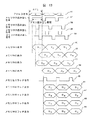
図17は、本発明になる前記画像信号処理装置による前記動画処理において、各ラインメモリ23〜26から読み出した出力データ信号64〜67を選択器50,51により同時化する方法を示している。同図において、64はラインメモリ23からの出力データ信号、65はラインメモリ24からの出力データ信号、66はラインメモリ25からの出力データ信号、67はラインメモリ26からの出力データ信号、50はデータ信号64とデータ信号65を同時化するための選択器、51はデータ信号66とデータ信号67を同時化するための選択器、52はこれらの選択器50,51の入力を切り換える切り換え信号、68はデータ信号64とデータ信号65を同時化した出力データ信号、69はデータ信号66とデータ信号67を同時化した出力データ信号を表わしている。
【0055】
選択器50,51は、切り換え信号52がハイレベルのときに上側の入力データ信号を選択し、切り換え信号52がローレベルのときに下側の入力データ信号を選択する。切り換え信号52のレベルの変化と選択器50,51の各出力データ信号68,69の関係は、図示のようになる。
【0056】
図18は、本発明になる画像信号処理装置において入力される画像(入力データ信号)をフレームメモリ2に記録する際の記録方式を示している。同図において、2はフレームメモリ、70はこのフレームメモリ2に記憶した1画面分の入力データのうちの左半画面分のデータ、71は残りの右半画面分のデータ、72は処理して再記憶した左半画面分の画像データ信号、73は最初に記憶したデータ信号70,71を処理た画像データ信号72をフレームメモリ2に再書き込みする際のアドレスの差分、74は最初に記憶したデータ信号70のうちで処理済みデータ信号72により上書きされずに残ったデータ信号70のアドレスの差分である。
【0057】
図10に示した方式で静止画を処理する場合、最初に、撮像素子18から出力される1フレーム分の入力データ信号1をフレームメモリ2に記憶する。このときは、水平方向にn画素分ずらした位置(水平方向のアドレスnの場所)からデータ信号70,71を書き始めるようにする。次に、記憶したデータのうち左半画面分のデータ信号70を読み出して信号処理を行ない、処理結果を処理済みデータ信号72として水平方向のアドレスが0の位置より書き始める。これによって、中央部より左のn画素が上書きされずに残るため、次に右半画面分のデータ信号71に対して水平方向の信号処理を行なうとき、中央部のデータ(左半画面のデータ70と右半画面のデータ71の境目)に対し連続的な処理が行なえるようになる。従って、画像に歪を生じることなくフルフレームの静止画を生成できるようになる。なお、この処理は、画面を水平方向にn分割し、現データ信号〜nライン遅延データ信号を生成し、処理する場合にも適用すると有効である。
【0058】
図19は、本発明になる画像信号処理装置における静止画処理のための遅延データ信号と動画処理のための遅延データ信号と共通の回路で生成するようにした信号遅延回路4の実施例を示している。同図において、1は入力データ信号、2はフレームメモリ、82はこのフレームメモリ2のアドレス信号、83はこのアドレス信号82を生成するメモリコントロール部、3は前記フレームメモリ2から出力したデータ信号、75は静止画処理と動画処理のときに該信号遅延回路4に入力するデータ信号を切り換える選択器、4はこの信号遅延回路、23は0.5Hの容量をもつ第1のラインメモリ、6は第1のラインメモリ23から出力されるデータ信号、24は0.5Hの容量をもつ第2のラインメモリ、7は第2のラインメモリ24から出力されるデータ信号、25は0.5Hの容量をもつ第3のラインメモリ、19は第3のラインメモリ25から出力されるデータ信号、26は0.5Hの容量をもつ第4のラインメモリ、20は第4のラインメモリ26から出力される手データ信号、50は第1のラインメモリ23から出力されたデータ信号6と第2のラインメモリ24から出力されたデータ信号7を切り換える選択器、53は選択器50から出力されるデータ信号、51は第3のラインメモリ24から出力されたデータ信号19と第4のラインメモリ26から出力されたデータ信号20を切り換える選択器、54は選択器51から出力されるデータ信号、27は前記各ラインメモリ23〜26に供給するアドレス信号、52は2系統のデータ信号を同時化するための切り換え信号、76は静止画処理と動画処理のときに第2のラインメモリ24の入力データ信号を切り換える選択器、77は静止画処理と動画処理のときに1ライン遅延データ信号の出力データを切り換える選択器、78は選択器77からの出力データ信号、79は静止画処理と動画処理のときに2ライン遅延データ信号の出力出たを切り換える選択器、80は選択器79からの出力データ信号、81は静止画処理と動画処理を切り換える切り換え信号を示している。
【0059】
静止画処理を行なう場合は、静止画処理/動画処理切り換え信号81をローレベルにする。そのとき、この信号遅延回路4の構成は、図11に示す信号遅延回路と等価になる。入力データ信号1は、フレームメモリ2に1画面分記憶する。このとき、水平方向のアドレスに数画素分のオフセットをもたせて書き込むようにする。次に、フレームメモリ2から、メモリコントロール部83によりノンインタレースで左半画面分(0.5H分)だけデータを読み出す。選択器75は、このとき、フレームメモリ2から出力されるデータ信号3を選択するので、信号遅延回路4にはこのデータ信号3が入力する。
【0060】
信号遅延回路4は、入力した現データ信号3を第1のラインメモリ23に送り、1ライン分遅延したデータ信号6を生成する。以下同様に、第2のラインメモリ24,第3のラインメモリ25,第4のラインメモリ26で、それぞれ、2ライン遅延デー信号7,3ライン遅延データ信号19,4ライン遅延データ信号20を生成する。選択器77では第1のラインメモリ23から出力されるデータ信号6を選択し、選択器79では第3のラインメモリ25から出力されるデータ信号19を選択することにより、該信号遅延回路4から1ライン遅延データ信号78と2ライン遅延データ信号80として出力する。選択器76では第3のラインメモリ25から出力されるデータ信号19を選択することにより、第2のラインメモリ24には第3のラインメモリ25から出力されるデータ信号19が入力して3ライン遅延データ信号7を生成する。また、第4のラインメモリ26には第2のラインメモリ24から出力されるデータ信号7が入力して4ライン遅延データ信号20を生成する。
【0061】
動画処理をする場合は、静止画処理/動画処理切り換え信号81をハイレベルにする。そのとき、この信号遅延回路4の構成は、図14に示す信号処理回路と等価になる。選択器75は、このとき、入力データ信号1を選択するので、信号遅延回路4にはこの入力データ信号1が入力する。信号遅延回路4に入力した入力データ信号1は、現データ信号21となる。この現データ信号21は、1H分のうちの0.5H分をラインメモリ23に記憶する。選択器76は現データ信号21を選択して、残りの0.5H分をラインメモリ24に記憶する。次の1H分の信号処理では、ラインメモリ23から出力されるデータ信号6をラインメモリ25に、ラインメモリ24から出力されるデータ信号7をラインメモリ26にそれぞれ記憶する。このときの入力データ信号,アドレス信号及びメモリ書き込み信号のタイミングは、図15に示すとおりである。
【0062】
また、ラインメモリ23,24から出力したデータ信号6,7は、選択器50で同時化して1ライン遅延データ信号53を生成する。そして、ラインメモリ25,26から出力したデータ信号19,20は、選択器51で同時化して2ライン遅延データ信号54を生成する。
【0063】
選択器77は1ライン遅延データ信号53を選択し、選択器79は2ライン遅延データ信号54を選択するので、この信号遅延回路4は、1ライン遅延データ信号78としてデータ信号53を出力し、2ライン遅延データ信号80としてデータ信号54を出力する。
【0064】
なお、各メモリに供給する書き込み信号,読み出し信号,アドレス信号は、図12,図13,図15,図16からわかるように、静止画処理と動画処理とで共通になり、同じタイミングで静止画/動画の信号処理ができるので回路規模を少なくすることができる。
【0065】
この結果、この処理回路によれば、フレームメモリ2及び2H分の容量のラインメモリ23〜26で、現データ信号〜4ライン遅延データ信号を使用する静止画処理と、現データ信号〜2ライン遅延データ信号を使用する動画処理とに対応することができ、回路規模とメモリ容量の削減を実現することができる。
【0066】
図20は、本発明になる画像信号処理装置における信号処理回路9のブロック図である。同図において、5は信号遅延回路4から出力される現データ信号、6は1ライン遅延データ信号、7は2ライン遅延データ信号、19は3ライン遅延データ信号、20は4ライン遅延データ信号、84は色信号生成回路、85は補色信号を分離及び補間する色分離回路、86は補色信号からRGB原色信号を生成するマトリクス回路、87はホワイトバランス回路、88はγ補正回路、89はRGB原色信号から色差信号を生成する色差マトリクス回路、21は色差信号、90は輝度信号生成回路、91は低域輝度信号生成回路、92は垂直エンハンサ信号生成回路、93は加算回路、22は輝度信号である。
【0067】
信号遅延回路4から出力される現データ信号5〜4ライン遅延データ信号20のうち、1ライン遅延データ信号6,2ライン遅延データ信号7,3ライン遅延データ信号19は、色分離回路85に入力する。色分離回路85は、入力した3ラインのデータ信号6,7,19から補色信号を分離及び補間し、マトリクス回路86に送る。マトリクス回路86は、入力した補色信号に対してマトリクス演算を行なってRGB原色信号を生成し、ホワイトバランス回路87に送る。ホワイトバランス回路87は、光源の明るさに応じてRGB原色信号のゲインを調節してγ補正回路88に送る。γ補正回路88は、入力したRGB原色信号にγ補正を施して色差マトリクス回路89に送る。色差マトリクス回路89は、入力したRGB原色信号に対してマトリクス演算を施して、R−Y,B−Yの色差信号21を生成する。
【0068】
輝度信号生成回路90は、現データ信号5〜4ライン遅延データ信号20を入力する。低域輝度信号生成回路91は、入力した2ライン遅延データ信号に対して、水平方向のフィルタ処理と輪郭補正を施して低域輝度信号を生成する。垂直エンハンサ信号生成回路92は、現データ信号5〜4ライン遅延データ信号20から垂直輪郭補正信号を生成する。加算回路93は、前記低域輝度信号と垂直輪郭補正信号を加算して輝度信号22を生成する。
【0069】
【発明の効果】
本発明によれば、1H分のメモリ容量があれば現データ信号〜nライン遅延データ信号を生成できるので、映像機器等において多数ラインによる垂直方向のフィルタリング等を行なうときなどに少ない容量のメモリで高画質な画像を得ることができる。
【0070】
また、デジタルカメにおける信号処理では、2H分の容量のメモリにより、現データ信号〜4ライン遅延データ信号を用いた静止画処理と現データ信号〜2ライン遅延データ信号を用いた動画処理を実現するることができ、高精細のフレーム静止画及びフィールド画(動画)を得ることができる。
【図面の簡単な説明】
【図1】本発明になる画像信号処理装置のブロック図である。
【図2】CCD撮像素子における画素混合読み出しの説明図である。
【図3】画素混合読み出しによる現データ信号,1ライン遅延データ信号,2ライン遅延データ信号の信号成分を示す説明図である。
【図4】CCD撮像素子におけるフレーム読み出しの説明図である。
【図5】フレーム読み出しによる現データ信号,1ライン遅延データ信号,2ライン遅延データ信号の信号成分を示す説明図である。
【図6】動画処理及び静止画処理における遅延データ信号を示す説明図である。
【図7】フレームメモリからデータを読み出す方法の説明図である。
【図8】本発明になる画像信号処理装置における信号遅延回路で現データ信号〜mライン遅延データ信号を得るための回路構成を詳述したブロック図である。
【図9】本発明になる画像信号処理装置における信号遅延回路で1ライン遅延データ信号を得るための回路構成を詳述したブロック図である。
【図10】本発明になる画像信号処理装置によりビデオカメラでフレーム静止画を生成及び記録するときの信号処理方式を説明するブロック図である。
【図11】本発明になる画像信号処理装置によりデジタルスチルカメラにおける静止画処理を行なうときのブロック図である。
【図12】静止画処理の際にメモリにデータを書き込むときのアドレス信号及び書き込み信号のタイミングを示すタイムチャートである。
【図13】静止画処理の際にメモリからデータを読み出すときのアドレス信号及び書き込み信号のタイミングを示すタイムチャートである。
【図14】本発明になる画像信号処理装置により動画処理を行なうときのブロック図である。
【図15】動画処理の際にメモリにデータを書き込むときのアドレス信号及び書き込み信号のタイミングを示すタイムチャートである。
【図16】動画処理の際にメモリからデータを読み出すときのアドレス信号及び書き込み信号のタイミングを示すタイムチャートである。
【図17】動画処理の際にメモリから読み出したデータを同時化するタイミングを示すタイムチャートである。
【図18】画面中央部の処理を連続した状態で行なうためにフレームメモリに対するデータの書き込みと読み出し方法を示す説明図である。
【図19】本発明になる画像信号処理装置により静止画処理なおけるデータ遅延と動画処理におけるデータ遅延と行なうためのブロック図である。
【図20】本発明になる画像信号処理装置における信号処理回路の詳細を示すブロック図である。
【符号の説明】
1…入力データ信号、 2…フレームメモリ、 4…信号処理回路、 3…読み出しデータ信号、 9…信号処理回路、 18…画素混合方式の撮像素子、 83…メモリコントロール部、23〜26…ラインメモリ。[0001]
[Industrial application fields]
The present invention relates to an image signal processing apparatus that generates moving image data and still image data in a video camera or the like.
[0002]
[Prior art]
With the spread of multimedia, a digital still camera has attracted attention as an interface for taking moving image data and still image data into a computer, a workstation or the like. When capturing a large amount of images, a still camera has advantages such as immediacy and economic efficiency compared to conventional scanners, and can be easily used because it can be reduced in size and weight. . For details about this process, see Television Society Vol. 46, no. 7 (1992) pp. 827-828.
[0003]
As an image sensor used to realize a digital still camera, a pixel mixture type image sensor generally used in current video cameras from the viewpoints of versatility and application of conventional video camera technology. It is desirable to use Further, in the case of using a pixel-mixing type image pickup device, there is an advantage that it can be used not only for moving image shooting but also for still image shooting by changing the readout method. Next, the explanation will be given.
[0004]
In moving image shooting using a pixel mixing type image sensor, field accumulation reading is performed. Field accumulation readout is a pixel mixing type CCD image pickup device in which data of upper and lower two pixels are mixed and read out in the device, and a typical filter arrangement is shown in FIG. In the first field, as shown in FIG. 2, the upper and lower lines are added for each horizontal scan, and signals are sequentially read out in the order of A1 and A2. Similarly, in the next field, the upper and lower lines are added for each horizontal scan, and are sequentially read out in the order of B1 and B2. As a result, (Mg + Ye), (G + Cy) and (G + Ye), (Mg + Cy) are alternately output from the sensor for each horizontal scan. Here, if Wr = Mg + Ye, Gb = G + Cy, Gr = G + Ye, and Wb = Mg + Cy, the data signal from the image sensor is the current data signal S. L 1 line delayed data signal S L-1 The data signal delayed by 2 lines is converted to S L-2 As shown in FIG.
[0005]
For still image recording using a pixel-mixing type image sensor, a frame-still image recording method for recording an image of one frame by interleaving the output data signal of each pixel-mixed field, and recording only an image of one field Field still image recording system. For the field still image recording method,
(1) Matrix correction as described in JP-A-1-143482 cannot be performed, and vertical color moire increases.
(2) The resolution in the vertical direction is insufficient and sufficient image quality cannot be obtained as a still image.
There is a problem. Accordingly, the frame still image recording method is desirable for still image recording. However, in the case of the frame still image recording method, there is a problem that a subject with a large amount of movement is blurred and a double image is formed.
[0006]
In order to solve such a problem, as shown in FIG. 4, in the first field, the data signal is read out without mixing the pixel data in the image sensor by one line every horizontal scanning, and in the next field. Similarly, a method has been developed in which a still image is recorded by reading out a data signal line by line for each horizontal scan. The data signal read in this way is as shown in FIG. According to this method, it is possible to obtain a still image that is free from blurring and does not deteriorate in resolution. This reading method is called a frame accumulation reading method, and this still image recording method is named a full frame still image recording method. Details of this are described in JP-A-4-274036 and JP-A-4-331393. The method will be described below.
[0007]
Reading a data signal from a pixel mixing type image sensor without pixel mixing can be realized by controlling the drive pulse of the image sensor. In order to realize the full frame still image recording method, it is necessary to sequentially read out image data signals by 1H (lines) in the order of filter arrangement arranged on the image sensor. However, since image data constituting one frame image is output from the image sensor every other line, one field at a time, and signal processing cannot be performed as it is. As a result of examination, a frame memory capable of storing image data for two fields (one frame) output from the image sensor was used, and one frame of the data signal output from the image sensor was stored in the frame memory. It was concluded that full frame still image recording would be possible if non-interlaced reading was performed later from the memory. As a result of examination by image simulation, it has been found that even with full-frame still image recording using a pixel-mixing type image sensor, recording with sufficient image quality can be obtained as a still image.
[0008]
When moving image processing is performed by performing field accumulation reading from the image sensor, both a color signal and a luminance signal are generated from data signals for three lines of a current data signal, a one-line delayed data signal, and a two-line delayed data signal. When still image processing is performed by performing frame accumulation and readout, the color signal is generated from the data signals for three lines of the 1-line delayed data signal, the 2-line delayed data signal, and the 3-line delayed data signal, and the luminance signal Are generated from the data signals for five lines of the current data signal, the 1-line delayed data signal, the 2-line delayed data signal, the 3-line delayed data signal, and the 4-line delayed data signal. FIG. 6 shows this state.
[0009]
In order to perform such image signal processing, it is understood that a delay circuit for generating a delay signal of an image data signal is indispensable for a video camera and other video equipment.
[0010]
[Problems to be solved by the invention]
In conventional digital signal processing, a memory is used as a delay circuit. However, when all the signal processing circuits are made into one chip in one IC, the specific gravity of the memory in the chip area and power consumption increases. When still image signal processing is performed, a line memory for 4H (lines) for generating a current data signal to a 4-line delayed data signal is required. If these line memories are to be built in an IC, the chip of the IC is used. Problems such as increased area and increased power consumption occur.
[0011]
Accordingly, an object of the present invention is to provide an image signal processing apparatus capable of reducing the memory used for delaying the image data signal.
[0012]
[Means for Solving the Problems]
In order to achieve this object, the present invention provides a frame memory for storing data for one screen, and a memory control for controlling the frame memory so as to read out data for each block by dividing one screen into n portions in the horizontal direction. , A first (1 / n) H line memory that stores data for one line ((1 / n) H) read from the frame memory, and data output from the first line memory A second (1 / n) H line memory for storing signals, a third (1 / n) H line memory for storing data signals output from the second line memory, and (m−1) The (m) (1 / n) H line memory for storing data signals output from the line memory and a memory control unit for controlling these memories are provided.
[0013]
[Action]
When a still image is taken with a pixel mixing type imaging device, the output data signal is in field units. The data signal is read and processed after being stored non-interlaced in the frame memory. In the case of a still image, unlike a moving image, real-time processing is not required, so that the screen can be divided and processed in the horizontal direction. Hereinafter, a procedure in the case of performing image processing by dividing into two in the horizontal direction will be described.
[0014]
(1) The data written in the frame memory is processed by reading the left half screen by (1/2) H.
[0015]
(2) The processing data for the left half screen is written again into the frame memory.
[0016]
(3) The remaining right half screen data is read and processed.
[0017]
(4) The processing data for the right half screen is written again into the frame memory.
[0018]
When still image processing is performed by this method, a memory of (1/2) H capacity is sufficient to delay data for one line. Therefore, the delayed data signal for 4 lines
(1/2) H × 4 = 2H min
It is possible to generate with the memory of capacity. In the case of moving image processing, real-time processing using a memory with a capacity of 2H is performed as usual, so that both moving images and still images can be processed with the memory for 2H.
[0019]
If a single screen is divided into a left half screen and a right half screen, if the signal processing is completely independent on the left half and the right half, discontinuous parts will appear at the boundary between the left and right screens. Resulting in distortion on the screen. This is because horizontal filtering is performed in signal processing, and the following measures are taken to prevent this discontinuity.
[0020]
When data is written from the image sensor to the frame memory, an offset for several pixels is previously given to the address in the horizontal direction. Next, when the processing result for the left half screen is written again into the frame memory, if the writing is started from
[0021]
As described above, the signal delay processing for generating the current data signal to the 4-line delayed data signal in the line memory having a capacity of 2H has been described for the signal processing of the digital camera. However, when still image processing is performed using the frame memory. More delayed data signals can be obtained by increasing the number of horizontal divisions.
[0022]
Here, a method of generating the current data signal to m line delayed data signal from the frame memory and the line memory for 1H will be described. When the data for one screen stored in the frame memory is output to the delay circuit, the data is read out for each block obtained by dividing one screen into n equal parts in the horizontal direction. The read data is stored in the first (1 / n) H line memory, and a one-line delayed data signal is generated. Next, a data signal output from the first line memory is stored in the second (1 / n) H line memory to generate a two-line delayed data signal. Similarly, the m-th (1 / n) ) The m line delayed data signal can be generated by the H line memory.
[0023]
In this manner, since a memory having a capacity of (1 / n) H is sufficient to generate a delayed data signal for one line, the current data signal to m-line delayed data signal are converted to (1 / n) H ×. It can be generated with a memory having a capacity of m = (m / n) H, and the amount of memory can be reduced when a large number of lines are used for vertical filtering or the like. Further, when performing real-time processing of a moving image, it can be used as an (m / n) H line memory.
[0024]
【Example】
Embodiments of the present invention will be described below with reference to the drawings.
[0025]
FIG. 1 is a block diagram of an image signal processing apparatus according to the present invention. This image signal processing apparatus has a circuit configuration that generates a current data signal to an m-line delayed data signal using m frame memories and m line memories having a capacity of (1 / n) H. Here, H is the number of image data (pixels) for one line in the horizontal direction.
[0026]
In FIG. 1, 1 is an input data signal, 2 is a frame memory, 3 is a data signal output from the
[0027]
The
[0028]
The
[0029]
Here, a method of reading data from the
[0030]
As shown in FIG. 7, the image data for one screen stored in the
[0031]
Next, generation of the current data signal 5 to m-line delayed data signal 8 by the
[0032]
As shown in FIG. 7, data is read from the
[0033]
Next, delay processing for generating a one-line delayed data signal in real time by the
[0034]
The first (1 / n) H portion of the input data signal 1 input to the
[0035]
FIG. 10 shows a signal processing method when a frame still image is generated and recorded in a video camera or the like using the image signal processing apparatus according to the present invention. In the figure,
[0036]
The input data signal 1 obtained by frame reading from the pixel-mixing
[0037]
FIG. 11 shows a circuit configuration in still image processing of a digital still camera using the image signal processing apparatus according to the present invention. In the figure, 1 is an input data signal, 2 is a frame memory, 3 is a data signal read from the
[0038]
The input data signal 1 is temporarily stored in the
[0039]
The
[0040]
FIG. 12 shows the timing of the address signal and the write signal when data is written to each of the
[0041]
The input data signal 28 and the
[0042]
FIG. 13 shows the timing of the address signal and read signal when reading data from each of the
[0043]
The
[0044]
FIG. 14 shows a delay processing circuit configuration for moving image processing by the image signal processing apparatus according to the present invention. In the figure, 4 is a signal delay circuit, 3 is an input data signal of the
[0045]
The data signal 3 for 1H input to the
[0046]
The data signals output from the
[0047]
FIG. 15 shows the timing of the address signal and write signal when data is written to the
[0048]
The input data signal 55 read from the image sensor at the sampling frequency fs (
[0049]
The
[0050]
The
[0051]
FIG. 16 shows the timing of the address signal and read signal when data is read from the
[0052]
The
[0053]
The read data signals 60 to 63 are aligned in phase by the
[0054]
FIG. 17 shows a method of synchronizing the output data signals 64 to 67 read from the
[0055]
The
[0056]
FIG. 18 shows a recording method when an image (input data signal) input in the image signal processing apparatus according to the present invention is recorded in the
[0057]
When a still image is processed by the method shown in FIG. 10, first, the input data signal 1 for one frame output from the
[0058]
FIG. 19 shows an embodiment of the
[0059]
When performing still image processing, the still image processing / moving image processing switching signal 81 is set to a low level. At that time, the configuration of the
[0060]
The
[0061]
When performing moving image processing, the still image processing / moving image processing switching signal 81 is set to the high level. At that time, the configuration of the
[0062]
The data signals 6 and 7 output from the
[0063]
Since the
[0064]
As can be seen from FIGS. 12, 13, 15, and 16, the write signal, read signal, and address signal supplied to each memory are common to the still image processing and the moving image processing. / Because video signal processing can be performed, the circuit scale can be reduced.
[0065]
As a result, according to this processing circuit, still image processing using the current data signal to the 4-line delayed data signal and the current data signal to the 2-line delay in the
[0066]
FIG. 20 is a block diagram of the
[0067]
Of the current data signal 5 to 4 line delay data signal 20 output from the
[0068]
The luminance signal generation circuit 90 inputs the current data signal 5 to 4 line delayed data signal 20. The low-frequency luminance signal generation circuit 91 generates a low-frequency luminance signal by performing horizontal filtering and contour correction on the input two-line delayed data signal. The vertical enhancer signal generation circuit 92 generates a vertical contour correction signal from the current data signal 5 to 4 line delayed data signal 20. The adder circuit 93 adds the low-frequency luminance signal and the vertical contour correction signal to generate a luminance signal 22.
[0069]
【The invention's effect】
According to the present invention, a current data signal to an n-line delayed data signal can be generated if there is a memory capacity for 1H, so that a memory with a small capacity can be used when performing vertical filtering by a large number of lines in video equipment or the like. A high-quality image can be obtained.
[0070]
In the signal processing in the digital camera, a still image processing using the current data signal to the 4-line delayed data signal and a moving image processing using the current data signal to the 2-line delayed data signal are realized by a memory having a capacity of 2H. High-definition frame still images and field images (moving images) can be obtained.
[Brief description of the drawings]
FIG. 1 is a block diagram of an image signal processing apparatus according to the present invention.
FIG. 2 is an explanatory diagram of pixel mixture readout in a CCD image sensor.
FIG. 3 is an explanatory diagram showing signal components of a current data signal, a one-line delayed data signal, and a two-line delayed data signal by pixel mixed readout.
FIG. 4 is an explanatory diagram of frame readout in a CCD image sensor.
FIG. 5 is an explanatory diagram showing signal components of a current data signal, a 1-line delayed data signal, and a 2-line delayed data signal by frame reading.
FIG. 6 is an explanatory diagram showing delayed data signals in moving image processing and still image processing.
FIG. 7 is an explanatory diagram of a method for reading data from a frame memory.
FIG. 8 is a block diagram detailing a circuit configuration for obtaining a current data signal to m-line delayed data signal by a signal delay circuit in the image signal processing apparatus according to the present invention;
FIG. 9 is a block diagram detailing a circuit configuration for obtaining a one-line delayed data signal by the signal delay circuit in the image signal processing apparatus according to the present invention;
FIG. 10 is a block diagram for explaining a signal processing method when a frame still image is generated and recorded by a video camera by the image signal processing apparatus according to the present invention.
FIG. 11 is a block diagram when still image processing is performed in a digital still camera by the image signal processing apparatus according to the present invention.
FIG. 12 is a time chart showing the timing of an address signal and a write signal when data is written to a memory during still image processing.
FIG. 13 is a time chart showing timings of an address signal and a write signal when data is read from the memory during still image processing.
FIG. 14 is a block diagram when moving image processing is performed by the image signal processing apparatus according to the present invention;
FIG. 15 is a time chart showing the timing of an address signal and a write signal when data is written to a memory during moving image processing.
FIG. 16 is a time chart showing the timing of an address signal and a write signal when reading data from a memory during moving image processing.
FIG. 17 is a time chart showing timing for synchronizing data read from a memory during moving image processing;
FIG. 18 is an explanatory diagram showing a method for writing and reading data to and from the frame memory in order to perform processing at the center of the screen in a continuous state.
FIG. 19 is a block diagram for performing data delay in still image processing and data delay in moving image processing by the image signal processing apparatus according to the present invention.
FIG. 20 is a block diagram showing details of a signal processing circuit in the image signal processing apparatus according to the present invention.
[Explanation of symbols]
DESCRIPTION OF
Claims (5)
前記メモリコントロール部(83)は、入力データ信号(1)を前記フレームメモリ(2)に記憶するように該フレームメモリ(2)を制御する第1の制御と、前記フレームメモリ(2)に記憶したデータを、画面を水平方向にn個のブロックに分割して分割したブロック毎に水平方向のデータ数が(1/n)H分のデータ信号(3)をライン順に読み出すようにフレームメモリ(2)のアドレス(82)を制御する第2の制御と、前記信号処理回路(9)の処理結果を再び前記フレームメモリ(2)の読み出したデータに上書きするか他の記憶媒体に記憶し、同様の処理をn個の全水平ブロックについて繰り返し行うことで、1画面分の信号処理を完了するように該フレームメモリ(2)または他の記憶媒体を制御し、処理結果の画像を出力する第3の制御を実行し、
前記信号遅延回路(4)は、(1/n)H分の容量のm個のラインメモリ(14〜16)を備え、前記第2の制御によりフレームメモリ(2)から読み出した画面を水平方向にn個のブロックに分割して該分割したブロック毎に水平方向のデータ数が(1/n)H分のデータ信号(3)をmライン分記憶することで、順次、各ブロック毎に現データ信号(5)〜mライン遅延データ信号(8)を生成することができる構成であって、静止画処理モードにおいては、前記フレームメモリ(2)から読み出したデータ信号(3)をmライン分記憶することで、順次、現データ信号(5)〜mライン遅延データ信号(8)を生成し、動画処理モードにおいては、前記入力データ信号(1)は、該フレームメモリ(2)を介在せず該信号遅延回路(4)に導びいて前記m個のラインメモリ(14〜16)をH分の記憶装置として使用し、
前記信号処理回路(9)は、各ブロック毎に、前記信号遅延回路(4)で生成した各遅延データ信号から画像信号を生成することを特徴とする画像信号処理装置。A frame memory (2), a memory control unit (83), a signal delay circuit (4), a signal processing circuit (9), and means for switching between two types of processing modes, a still image processing mode and a moving image processing mode (75) , 76) ,
The memory control unit (83) stores in the frame memory (2) a first control for controlling the frame memory (2) so as to store the input data signal (1) in the frame memory (2). The frame memory (1) reads the data signal (3) corresponding to the number of data in the horizontal direction (1 / n) H for each block obtained by dividing the screen into n blocks in the horizontal direction. 2) the second control for controlling the address (82) and the processing result of the signal processing circuit (9) are overwritten again on the data read from the frame memory (2) or stored in another storage medium, By repeating the same process for all n horizontal blocks, the frame memory (2) or other storage medium is controlled so that the signal processing for one screen is completed, and an image of the processing result is output. Run the third control that,
The signal delay circuit (4) includes m line memories (14 to 16) having a capacity of (1 / n) H, and the screen read from the frame memory (2) by the second control is horizontally By dividing the block into n blocks and storing the data signal (3) corresponding to (1 / n) H in the horizontal direction for each divided block for m lines, each block is The data signal (5) to the m-line delayed data signal (8) can be generated . In the still image processing mode, the data signal (3) read from the frame memory (2) is output for m lines. The current data signal (5) to m-line delayed data signal (8) are sequentially generated by storing, and in the moving image processing mode, the input data signal (1) is interposed in the frame memory (2). The signal delay circuit (4 Using the Te Shirubebii m pieces of line memories (14-16) as H min of the storage device,
The image signal processing apparatus, wherein the signal processing circuit (9) generates an image signal from each delayed data signal generated by the signal delay circuit (4) for each block.
この画像信号処理装置は、静止画処理モードと動画処理モードの2種の処理モードを切り替える手段を備え、
静止画処理モードにおいては、
前記撮像素子(18)から出力したデータ信号(1)をフレームメモリ(2)に1フレーム分記憶し、記憶したデータを左半画面ブロックと右半画面ブロックとに分けて各ブロック毎に前記データを1ラインづつライン順に出力するようにフレームメモリ(2)を制御するメモリコントロール部(82)と、
前記フレームメモリ(2)から出力した1/2H分の現データ信号(3)と、該現データ信号(3)を1ライン遅延した1ライン遅延データ信号(6)と、該1ライン遅延データ信号(6)を1ライン遅延した2ライン遅延データ信号(7)と、該2ライン遅延データ信号(7)を1ライン遅延した3ライン遅延データ信号(19)と、該3ライン遅延データ信号(19)を1ライン遅延した4ライン遅延データ信号(20)とを生成する信号遅延回路(4)と、
前記信号遅延回路(4)で生成した前記現データ信号(5)と1ライン遅延データ信号(6)と2ライン遅延データ信号(7)と3ライン遅延データ信号(19)と4ライン遅延データ信号(20)から映像の色信号(21)と輝度信号(22)を生成する信号処理回路(9)とを有効にして、
前記メモリコントロール部(82)により前記フレームメモリ(2)を制御し、前記信号処理回路(9)で生成した前記色信号(21)と輝度信号(21)を前記フレームメモリ(2)から読み出したデータ信号(3)上に上書きするか他の記憶媒体に出力することで静止画を得、
動画処理モードにおいては、
前記撮像素子(18)から出力されたデータ信号(1)より、1H分の現データ信号(3)と、該現データ信号(3)を1ライン遅延した1ライン遅延データ信号(53)と、該1ライン遅延データ信号(53)を1ライン遅延した2ライン遅延データ信号(54)とを生成する信号遅延回路(4)と、
前記信号遅延回路(4)で生成した前記現データ信号(3)と1ライン遅延データ信号(53)と2ライン遅延データ信号(54)から映像の色信号(21)と輝度信号(22)を生成する信号処理回路(9)とを有効にして動画を得ることを特徴とする画像信号処理装置。A plurality of color filters having different spectral sensitivities are provided, and in one horizontal line, a data signal generated from a photoelectric conversion element having a color filter corresponding to the first color and the second color is output, and the next horizontal line , An image sensor (18) that outputs a data signal generated from a photoelectric conversion element having color filters corresponding to the third color and the fourth color, a frame memory (2), and a memory control unit (83) ), A signal delay circuit (4), and a signal processing circuit (9),
The image signal processing apparatus includes means for switching between two processing modes, a still image processing mode and a moving image processing mode,
In still image processing mode,
The data signal (1) output from the image sensor (18) is stored in the frame memory (2) for one frame, and the stored data is divided into a left half screen block and a right half screen block, and the data for each block. A memory control unit (82) for controlling the frame memory (2) so as to output in order line by line,
The current data signal (3) for 1 / 2H output from the frame memory (2), a one-line delayed data signal (6) obtained by delaying the current data signal (3) by one line, and the one-line delayed data signal A two-line delayed data signal (7) obtained by delaying (6) by one line, a three-line delayed data signal (19) obtained by delaying the two-line delayed data signal (7) by one line, and the three-line delayed data signal (19) A signal delay circuit (4) for generating a 4-line delayed data signal (20) delayed by 1 line;
The current data signal (5), 1-line delayed data signal (6), 2-line delayed data signal (7), 3-line delayed data signal (19), and 4-line delayed data signal generated by the signal delay circuit (4). The signal processing circuit (9) that generates the color signal (21) and the luminance signal (22) of the video from (20) is enabled,
The frame controller (82) is controlled by the memory control unit (82), and the color signal (21) and the luminance signal (21) generated by the signal processing circuit (9) are read from the frame memory (2). A still image is obtained by overwriting on the data signal (3) or outputting to another storage medium,
In the video processing mode,
From the data signal (1) output from the image sensor (18), a current data signal (3) for 1H, a one-line delayed data signal (53) obtained by delaying the current data signal (3) by one line, A signal delay circuit (4) for generating a two-line delayed data signal (54) obtained by delaying the one-line delayed data signal (53) by one line;
An image color signal (21) and a luminance signal (22) are generated from the current data signal (3), the one-line delayed data signal (53), and the two-line delayed data signal (54) generated by the signal delay circuit (4). An image signal processing apparatus characterized in that a moving image is obtained by enabling a signal processing circuit (9) to be generated.
静止画処理モードにおいては、
前記フレームメモリ(2)より出力される半画面分のデータ信号を前記第1のラインメモリ(23)に1ライン((1/2)H)分記憶して1ライン遅延データ信号(6)を生成し、第1のラインメモリ(23)より出力されるデータ信号を前記第2のラインメモリ(24)に1ライン分記憶して2ライン遅延データ信号(7)を生成し、
前記第2のラインメモリ(24)より出力されるデータ信号を前記第3のラインメモリ(25)に1ライン分記憶して3ライン遅延データ信号(19)を生成し、
前記第3のラインメモリ(25)より出力されるデータ信号を前記第4のラインメモリ(25)に1ライン分記憶して4ライン遅延データ信号(20)を生成し、
動画処理モードにおいては、
1Hづつ入力される入力データ信号(1)に対して、該入力データ信号(1)を、前記第1のラインメモリ(23)と第2のラインメモリ(24)に記憶し、
前記第1のラインメモリ(23)から読み出されるデータ信号を前記第3のラインメモリ(25)に記憶し、
前記第2のラインメモリ(24)から読み出されるデータ信号を前記第4のラインメモリ(26)に記憶し、
前記第1のラインメモリ(23)と第2のラインメモリ(24)から出力されるデータ信号を第1の選択器(50)により切り換えることで1ライン遅延データ信号(6)をリアルタイムで生成し、
前記第3のラインメモリ(25)と第4のラインメモリ(26)から出力されるデータ信号を第2の選択器(51)により切り換えることで2ライン遅延データ信号(7)をリアルタイムで生成することを特徴とする画像信号処理装置。4. The signal delay circuit (4) according to claim 3 , wherein the signal delay circuit (4) includes a first line memory (23) having a capacity of (1/2) H and a second line having a capacity of (1/2) H. A memory (24), a third line memory (25) having a capacity of (1/2) H, and a fourth line memory (26) having a capacity of (1/2) H, The signal delay circuit (4) includes two processing modes, a still image processing mode and a moving image processing mode, and means for switching between them.
In still image processing mode,
A half-screen data signal output from the frame memory (2) is stored in the first line memory (23) for one line ((1/2) H), and a one-line delayed data signal (6) is stored. Generating a data signal output from the first line memory (23) for one line in the second line memory (24) to generate a two-line delayed data signal (7);
A data signal output from the second line memory (24) is stored for one line in the third line memory (25) to generate a three-line delayed data signal (19),
A data signal output from the third line memory (25) is stored for one line in the fourth line memory (25) to generate a four-line delayed data signal (20),
In the video processing mode,
With respect to the input data signal (1) inputted in 1H increments, the input data signal (1) is stored in the first line memory (23) and the second line memory (24),
Storing a data signal read from the first line memory (23) in the third line memory (25);
Storing the data signal read from the second line memory (24) in the fourth line memory (26);
By switching the data signals output from the first line memory (23) and the second line memory (24) by the first selector (50), a one-line delayed data signal (6) is generated in real time. ,
A data signal output from the third line memory (25) and the fourth line memory (26) is switched by a second selector (51) to generate a two-line delayed data signal (7) in real time. An image signal processing apparatus.
前記入力データ信号(1)を前記フレームメモリ(2)に1フレーム分記憶し、記憶したデータを左半画面ブロックと右半画面ブロックとに分けて各ブロック毎に読み出すように前記フレームメモリ(2)を制御するメモリコントロール部(82)と、
(1/2)H分の容量をもち、前記第1の選択器(75)から出力されるデータ信号を(1/2)H分記憶する第1のラインメモリ(23)と、
(1/2)H分の容量をもち、前記第1のラインメモリ(23)から出力されるデータ信号(6)を(1/2)H分記憶する第2のラインメモリ(25)と、
前記入力データ信号(1)とラインメモリ(25)から出力されるデータ(19)を切り換える第2の選択器(76)と、
(1/2)H分の容量をもち、前記第2の選択器(76)から出力されるデータ信号を(1/2)H分記憶する第3のラインメモリ(24)と、
(1/2)H分の容量をもち、前記第3のラインメモリ(24)から出力されるデータ信号を(1/2)H分記憶する第4のラインメモリ(26)と、
前記第1のラインメモリ(23)と第3のラインメモリ(24)から出力されるデータ信号を切り換えて1ライン遅延データ信号を生成するする第3の選択器(50)と、
前記第2のラインメモリ(25)と第4のラインメモリ(26)から出力されるデータ信号を切り換えて2ライン遅延データ信号を生成する第4の選択器(51)と、
前記第1のラインメモリ(23)から出力されるデータ信号(6)と第3の選択器(50)から出力されるデータ信号(53)を切り換える第5の選択器(78)と、
前記第2のラインメモリ(25)から出力されるデータ信号(19)と第4の選択器(51)から出力されるデータ信号(54)を切り換える第6の選択器(79)とを備え、
前記第1の選択器(75)と第2の選択器(76)と第5の選択器(77)と第6の選択器(79)を同時に切り換えることで、
静止画処理の場合は、前記フレームメモリ(2)から出力されるデータ信号(3)を前記ラインメモリ(23)に記憶し、該ラインメモリ(23)から出力されるデータ信号は前記ラインメモリ(25)に記憶し、前記ラインメモリ(25)から出力されるデータ信号はラインメモリ(24)に記憶し、前記ラインメモリ(24)から出力されるデータ信号はラインメモリ(26)に記憶し、
前記フレームメモリ(2)から入力した現データ信号(3)と、該第1のラインメモリ(23)で生成した1ライン遅延データ信号(6)と、該第2のラインメモリ(24)で生成した2ライン遅延データ信号(7)と、該第3のラインメモリ(25)で生成した3ライン遅延データ信号(19)と、該第4のラインメモリ(26)で生成した4ライン遅延データ信号(20)とを出力し、
動画処理の場合は、入力データ信号(1)を第1のラインメモリ(23)と第2のラインメモリ(24)に記憶し、
前記第1のラインメモリ(23)から読み出されるデータ信号を第3のラインメモリ(25)記憶し、前記第2のラインメモリ(24)から読み出されるデータ信号を第4のラインメモリ(26)に記憶し、
前記第1のラインメモリ(23)と第2のラインメモリ(24)から出力されるデータ信号から第1の選択器(50)で1ライン遅延データ信号(6)を生成し、
前記第3のラインメモリ(25)と第4のラインメモリ(26)から出力されるデータ信号から第2の選択器(51)で2ライン遅延データ信号(7)を生成することを特徴とする画像信号処理装置。A frame memory (2) for storing the input data signal (1) for one frame, and a first selector (75) for switching between the input data signal (1) and the data (3) output from the frame memory (2) )When,
The input data signal (1) is stored in the frame memory (2) for one frame, and the stored data is divided into a left half screen block and a right half screen block, and the frame memory (2 A memory control unit (82) for controlling
A first line memory (23) having a capacity of (1/2) H and storing the data signal output from the first selector (75) for (1/2) H;
A second line memory (25) having a capacity of (1/2) H and storing the data signal (6) output from the first line memory (23) for (1/2) H;
A second selector (76) for switching the input data signal (1) and the data (19) output from the line memory (25);
A third line memory (24) having a capacity of (1/2) H and storing a data signal output from the second selector (76) for (1/2) H;
A fourth line memory (26) having a capacity of (1/2) H and storing the data signal output from the third line memory (24) for (1/2) H;
A third selector (50) for generating a one-line delayed data signal by switching data signals output from the first line memory (23) and the third line memory (24);
A fourth selector (51) for switching data signals output from the second line memory (25) and the fourth line memory (26) to generate a two-line delayed data signal;
A fifth selector (78) for switching the data signal (6) output from the first line memory (23) and the data signal (53) output from the third selector (50);
A sixth selector (79) for switching a data signal (19) output from the second line memory (25) and a data signal (54) output from the fourth selector (51);
By simultaneously switching the first selector (75), the second selector (76), the fifth selector (77), and the sixth selector (79),
In the case of still image processing, the data signal (3) output from the frame memory (2) is stored in the line memory (23), and the data signal output from the line memory (23) is stored in the line memory (23). 25), the data signal output from the line memory (25) is stored in the line memory (24), the data signal output from the line memory (24) is stored in the line memory (26),
Generated by the current data signal (3) input from the frame memory (2), the one-line delayed data signal (6) generated by the first line memory (23), and the second line memory (24) 2-line delayed data signal (7), 3-line delayed data signal (19) generated by the third line memory (25), and 4-line delayed data signal generated by the fourth line memory (26) (20) is output,
In the case of moving image processing, the input data signal (1) is stored in the first line memory (23) and the second line memory (24),
A data signal read from the first line memory (23) is stored in a third line memory (25), and a data signal read from the second line memory (24) is stored in a fourth line memory (26). Remember,
A 1-line delayed data signal (6) is generated by a first selector (50) from data signals output from the first line memory (23) and the second line memory (24),
A two-line delayed data signal (7) is generated by a second selector (51) from data signals output from the third line memory (25) and the fourth line memory (26). Image signal processing device.
Priority Applications (1)
| Application Number | Priority Date | Filing Date | Title |
|---|---|---|---|
| JP02290795A JP3671448B2 (en) | 1995-02-10 | 1995-02-10 | Image signal processing device |
Applications Claiming Priority (1)
| Application Number | Priority Date | Filing Date | Title |
|---|---|---|---|
| JP02290795A JP3671448B2 (en) | 1995-02-10 | 1995-02-10 | Image signal processing device |
Publications (2)
| Publication Number | Publication Date |
|---|---|
| JPH08221562A JPH08221562A (en) | 1996-08-30 |
| JP3671448B2 true JP3671448B2 (en) | 2005-07-13 |
Family
ID=12095717
Family Applications (1)
| Application Number | Title | Priority Date | Filing Date |
|---|---|---|---|
| JP02290795A Expired - Fee Related JP3671448B2 (en) | 1995-02-10 | 1995-02-10 | Image signal processing device |
Country Status (1)
| Country | Link |
|---|---|
| JP (1) | JP3671448B2 (en) |
Families Citing this family (1)
| Publication number | Priority date | Publication date | Assignee | Title |
|---|---|---|---|---|
| JP3932006B2 (en) | 1998-12-02 | 2007-06-20 | 株式会社日立製作所 | Imaging device |
-
1995
- 1995-02-10 JP JP02290795A patent/JP3671448B2/en not_active Expired - Fee Related
Also Published As
| Publication number | Publication date |
|---|---|
| JPH08221562A (en) | 1996-08-30 |
Similar Documents
| Publication | Publication Date | Title |
|---|---|---|
| US7034868B2 (en) | Image processing circuit | |
| US6342921B1 (en) | Lattice-type solid state image pickup device | |
| JP2000092376A (en) | Image pickup device | |
| JP2000092361A (en) | Image pickup device | |
| US20020196349A1 (en) | Image processing of video signal for display | |
| US6762792B1 (en) | Digital still camera | |
| JP2000092375A (en) | Signal processing unit and its control method | |
| JP3962928B2 (en) | Image data conversion method, conversion circuit, and imaging apparatus | |
| JP3671448B2 (en) | Image signal processing device | |
| JP2004260265A (en) | Pixel extracting circuit having pixel turning over function, and image pickup apparatus | |
| JP4260769B2 (en) | Image processing circuit | |
| JP2000092365A (en) | Signal processing unit | |
| US6266101B1 (en) | Y/C separator | |
| JP3489852B2 (en) | High-definition imaging device | |
| JP2002258814A (en) | Liquid crystal drive device | |
| JP2002359856A (en) | Data conversion circuit and digital camera | |
| JPH08149361A (en) | Digital camera | |
| JP2000092349A (en) | Image processor | |
| JP3615154B2 (en) | Image conversion apparatus and image conversion method | |
| JP2000228774A (en) | Image signal processing unit and electronic still camera provided with the same | |
| JP2007243819A (en) | Image processing apparatus | |
| JP4249909B2 (en) | Signal processing apparatus and signal processing method | |
| JP3603683B2 (en) | Video encoder circuit and television system conversion method | |
| JP3400649B2 (en) | Image synthesizing method in monitor device and monitoring camera device | |
| JP2005006078A (en) | Image pickup device |
Legal Events
| Date | Code | Title | Description |
|---|---|---|---|
| A131 | Notification of reasons for refusal |
Free format text: JAPANESE INTERMEDIATE CODE: A131 Effective date: 20040518 |
|
| A521 | Request for written amendment filed |
Free format text: JAPANESE INTERMEDIATE CODE: A523 Effective date: 20040712 |
|
| A02 | Decision of refusal |
Free format text: JAPANESE INTERMEDIATE CODE: A02 Effective date: 20041116 |
|
| A521 | Request for written amendment filed |
Free format text: JAPANESE INTERMEDIATE CODE: A523 Effective date: 20041216 |
|
| A911 | Transfer to examiner for re-examination before appeal (zenchi) |
Free format text: JAPANESE INTERMEDIATE CODE: A911 Effective date: 20050131 |
|
| TRDD | Decision of grant or rejection written | ||
| A01 | Written decision to grant a patent or to grant a registration (utility model) |
Free format text: JAPANESE INTERMEDIATE CODE: A01 Effective date: 20050329 |
|
| A61 | First payment of annual fees (during grant procedure) |
Free format text: JAPANESE INTERMEDIATE CODE: A61 Effective date: 20050411 |
|
| R150 | Certificate of patent or registration of utility model |
Free format text: JAPANESE INTERMEDIATE CODE: R150 |
|
| FPAY | Renewal fee payment (event date is renewal date of database) |
Free format text: PAYMENT UNTIL: 20090428 Year of fee payment: 4 |
|
| FPAY | Renewal fee payment (event date is renewal date of database) |
Free format text: PAYMENT UNTIL: 20090428 Year of fee payment: 4 |
|
| FPAY | Renewal fee payment (event date is renewal date of database) |
Free format text: PAYMENT UNTIL: 20100428 Year of fee payment: 5 |
|
| FPAY | Renewal fee payment (event date is renewal date of database) |
Free format text: PAYMENT UNTIL: 20110428 Year of fee payment: 6 |
|
| FPAY | Renewal fee payment (event date is renewal date of database) |
Free format text: PAYMENT UNTIL: 20120428 Year of fee payment: 7 |
|
| FPAY | Renewal fee payment (event date is renewal date of database) |
Free format text: PAYMENT UNTIL: 20120428 Year of fee payment: 7 |
|
| FPAY | Renewal fee payment (event date is renewal date of database) |
Free format text: PAYMENT UNTIL: 20130428 Year of fee payment: 8 |
|
| FPAY | Renewal fee payment (event date is renewal date of database) |
Free format text: PAYMENT UNTIL: 20140428 Year of fee payment: 9 |
|
| S111 | Request for change of ownership or part of ownership |
Free format text: JAPANESE INTERMEDIATE CODE: R313115 |
|
| R350 | Written notification of registration of transfer |
Free format text: JAPANESE INTERMEDIATE CODE: R350 |
|
| LAPS | Cancellation because of no payment of annual fees |