JP3671233B2 - Light emitting display element - Google Patents
Light emitting display element Download PDFInfo
- Publication number
- JP3671233B2 JP3671233B2 JP19520396A JP19520396A JP3671233B2 JP 3671233 B2 JP3671233 B2 JP 3671233B2 JP 19520396 A JP19520396 A JP 19520396A JP 19520396 A JP19520396 A JP 19520396A JP 3671233 B2 JP3671233 B2 JP 3671233B2
- Authority
- JP
- Japan
- Prior art keywords
- yttrium oxide
- film
- cathode electrode
- light
- yttrium
- Prior art date
- Legal status (The legal status is an assumption and is not a legal conclusion. Google has not performed a legal analysis and makes no representation as to the accuracy of the status listed.)
- Expired - Fee Related
Links
- SIWVEOZUMHYXCS-UHFFFAOYSA-N oxo(oxoyttriooxy)yttrium Chemical compound O=[Y]O[Y]=O SIWVEOZUMHYXCS-UHFFFAOYSA-N 0.000 claims description 151
- 229910052727 yttrium Inorganic materials 0.000 claims description 50
- VWQVUPCCIRVNHF-UHFFFAOYSA-N yttrium atom Chemical group [Y] VWQVUPCCIRVNHF-UHFFFAOYSA-N 0.000 claims description 49
- 230000005525 hole transport Effects 0.000 claims description 30
- 239000013078 crystal Substances 0.000 claims description 24
- 229910001404 rare earth metal oxide Inorganic materials 0.000 claims description 20
- 229910052761 rare earth metal Inorganic materials 0.000 claims description 13
- 239000004020 conductor Substances 0.000 claims description 10
- 239000010408 film Substances 0.000 description 207
- 239000010410 layer Substances 0.000 description 111
- QVGXLLKOCUKJST-UHFFFAOYSA-N atomic oxygen Chemical compound [O] QVGXLLKOCUKJST-UHFFFAOYSA-N 0.000 description 66
- 239000001301 oxygen Substances 0.000 description 66
- 229910052760 oxygen Inorganic materials 0.000 description 66
- 239000000758 substrate Substances 0.000 description 54
- 239000001257 hydrogen Substances 0.000 description 39
- 229910052739 hydrogen Inorganic materials 0.000 description 39
- 239000000463 material Substances 0.000 description 39
- UFHFLCQGNIYNRP-UHFFFAOYSA-N Hydrogen Chemical compound [H][H] UFHFLCQGNIYNRP-UHFFFAOYSA-N 0.000 description 37
- 239000007789 gas Substances 0.000 description 34
- 238000004519 manufacturing process Methods 0.000 description 33
- 239000012298 atmosphere Substances 0.000 description 31
- 238000000034 method Methods 0.000 description 30
- OAICVXFJPJFONN-UHFFFAOYSA-N Phosphorus Chemical compound [P] OAICVXFJPJFONN-UHFFFAOYSA-N 0.000 description 16
- 238000010438 heat treatment Methods 0.000 description 16
- 238000002441 X-ray diffraction Methods 0.000 description 14
- 230000003647 oxidation Effects 0.000 description 14
- 238000007254 oxidation reaction Methods 0.000 description 14
- 239000002585 base Substances 0.000 description 13
- XKRFYHLGVUSROY-UHFFFAOYSA-N Argon Chemical compound [Ar] XKRFYHLGVUSROY-UHFFFAOYSA-N 0.000 description 12
- 239000000126 substance Substances 0.000 description 12
- PXHVJJICTQNCMI-UHFFFAOYSA-N nickel Substances [Ni] PXHVJJICTQNCMI-UHFFFAOYSA-N 0.000 description 11
- 230000001590 oxidative effect Effects 0.000 description 11
- VYPSYNLAJGMNEJ-UHFFFAOYSA-N Silicium dioxide Chemical compound O=[Si]=O VYPSYNLAJGMNEJ-UHFFFAOYSA-N 0.000 description 9
- 229910021417 amorphous silicon Inorganic materials 0.000 description 9
- 230000015572 biosynthetic process Effects 0.000 description 9
- XLYOFNOQVPJJNP-UHFFFAOYSA-N water Chemical compound O XLYOFNOQVPJJNP-UHFFFAOYSA-N 0.000 description 9
- 229910052782 aluminium Inorganic materials 0.000 description 8
- 238000004544 sputter deposition Methods 0.000 description 8
- 238000002834 transmittance Methods 0.000 description 8
- TVIVIEFSHFOWTE-UHFFFAOYSA-K tri(quinolin-8-yloxy)alumane Chemical compound [Al+3].C1=CN=C2C([O-])=CC=CC2=C1.C1=CN=C2C([O-])=CC=CC2=C1.C1=CN=C2C([O-])=CC=CC2=C1 TVIVIEFSHFOWTE-UHFFFAOYSA-K 0.000 description 8
- 238000010521 absorption reaction Methods 0.000 description 7
- 238000006243 chemical reaction Methods 0.000 description 7
- 238000006356 dehydrogenation reaction Methods 0.000 description 7
- 229910052786 argon Inorganic materials 0.000 description 6
- 230000004888 barrier function Effects 0.000 description 6
- 238000007733 ion plating Methods 0.000 description 6
- 239000000203 mixture Substances 0.000 description 6
- 229910052759 nickel Inorganic materials 0.000 description 6
- 239000010453 quartz Substances 0.000 description 6
- XAGFODPZIPBFFR-UHFFFAOYSA-N aluminium Chemical compound [Al] XAGFODPZIPBFFR-UHFFFAOYSA-N 0.000 description 5
- 239000012300 argon atmosphere Substances 0.000 description 5
- 230000005540 biological transmission Effects 0.000 description 5
- 239000011651 chromium Substances 0.000 description 5
- 230000007423 decrease Effects 0.000 description 5
- 150000002431 hydrogen Chemical class 0.000 description 5
- 238000002347 injection Methods 0.000 description 5
- 239000007924 injection Substances 0.000 description 5
- 229910052688 Gadolinium Inorganic materials 0.000 description 4
- XLOMVQKBTHCTTD-UHFFFAOYSA-N Zinc monoxide Chemical compound [Zn]=O XLOMVQKBTHCTTD-UHFFFAOYSA-N 0.000 description 4
- 229910052804 chromium Inorganic materials 0.000 description 4
- 238000010894 electron beam technology Methods 0.000 description 4
- 230000003287 optical effect Effects 0.000 description 4
- 230000006798 recombination Effects 0.000 description 4
- 238000005215 recombination Methods 0.000 description 4
- 229910052684 Cerium Inorganic materials 0.000 description 3
- 229910052692 Dysprosium Inorganic materials 0.000 description 3
- 229910052691 Erbium Inorganic materials 0.000 description 3
- 229910052693 Europium Inorganic materials 0.000 description 3
- 229910052689 Holmium Inorganic materials 0.000 description 3
- 229910052765 Lutetium Inorganic materials 0.000 description 3
- 229910052779 Neodymium Inorganic materials 0.000 description 3
- 229910052777 Praseodymium Inorganic materials 0.000 description 3
- 229910052773 Promethium Inorganic materials 0.000 description 3
- 229910052772 Samarium Inorganic materials 0.000 description 3
- 229910052771 Terbium Inorganic materials 0.000 description 3
- 229910052775 Thulium Inorganic materials 0.000 description 3
- 229910052769 Ytterbium Inorganic materials 0.000 description 3
- 229910052783 alkali metal Inorganic materials 0.000 description 3
- 150000001340 alkali metals Chemical class 0.000 description 3
- 229910052784 alkaline earth metal Inorganic materials 0.000 description 3
- 150000001342 alkaline earth metals Chemical class 0.000 description 3
- GWXLDORMOJMVQZ-UHFFFAOYSA-N cerium Chemical compound [Ce] GWXLDORMOJMVQZ-UHFFFAOYSA-N 0.000 description 3
- VBVAVBCYMYWNOU-UHFFFAOYSA-N coumarin 6 Chemical compound C1=CC=C2SC(C3=CC4=CC=C(C=C4OC3=O)N(CC)CC)=NC2=C1 VBVAVBCYMYWNOU-UHFFFAOYSA-N 0.000 description 3
- KBQHZAAAGSGFKK-UHFFFAOYSA-N dysprosium atom Chemical compound [Dy] KBQHZAAAGSGFKK-UHFFFAOYSA-N 0.000 description 3
- 230000000694 effects Effects 0.000 description 3
- 239000007772 electrode material Substances 0.000 description 3
- UYAHIZSMUZPPFV-UHFFFAOYSA-N erbium Chemical compound [Er] UYAHIZSMUZPPFV-UHFFFAOYSA-N 0.000 description 3
- OGPBJKLSAFTDLK-UHFFFAOYSA-N europium atom Chemical compound [Eu] OGPBJKLSAFTDLK-UHFFFAOYSA-N 0.000 description 3
- UIWYJDYFSGRHKR-UHFFFAOYSA-N gadolinium atom Chemical compound [Gd] UIWYJDYFSGRHKR-UHFFFAOYSA-N 0.000 description 3
- KJZYNXUDTRRSPN-UHFFFAOYSA-N holmium atom Chemical compound [Ho] KJZYNXUDTRRSPN-UHFFFAOYSA-N 0.000 description 3
- 239000012535 impurity Substances 0.000 description 3
- OHSVLFRHMCKCQY-UHFFFAOYSA-N lutetium atom Chemical compound [Lu] OHSVLFRHMCKCQY-UHFFFAOYSA-N 0.000 description 3
- 239000011572 manganese Substances 0.000 description 3
- 229910052751 metal Inorganic materials 0.000 description 3
- 239000002184 metal Substances 0.000 description 3
- 229910052750 molybdenum Inorganic materials 0.000 description 3
- QEFYFXOXNSNQGX-UHFFFAOYSA-N neodymium atom Chemical compound [Nd] QEFYFXOXNSNQGX-UHFFFAOYSA-N 0.000 description 3
- RUDFQVOCFDJEEF-UHFFFAOYSA-N oxygen(2-);yttrium(3+) Chemical class [O-2].[O-2].[O-2].[Y+3].[Y+3] RUDFQVOCFDJEEF-UHFFFAOYSA-N 0.000 description 3
- PUDIUYLPXJFUGB-UHFFFAOYSA-N praseodymium atom Chemical compound [Pr] PUDIUYLPXJFUGB-UHFFFAOYSA-N 0.000 description 3
- VQMWBBYLQSCNPO-UHFFFAOYSA-N promethium atom Chemical compound [Pm] VQMWBBYLQSCNPO-UHFFFAOYSA-N 0.000 description 3
- 150000002910 rare earth metals Chemical class 0.000 description 3
- KZUNJOHGWZRPMI-UHFFFAOYSA-N samarium atom Chemical compound [Sm] KZUNJOHGWZRPMI-UHFFFAOYSA-N 0.000 description 3
- GZCRRIHWUXGPOV-UHFFFAOYSA-N terbium atom Chemical compound [Tb] GZCRRIHWUXGPOV-UHFFFAOYSA-N 0.000 description 3
- FRNOGLGSGLTDKL-UHFFFAOYSA-N thulium atom Chemical compound [Tm] FRNOGLGSGLTDKL-UHFFFAOYSA-N 0.000 description 3
- NAWDYIZEMPQZHO-UHFFFAOYSA-N ytterbium Chemical compound [Yb] NAWDYIZEMPQZHO-UHFFFAOYSA-N 0.000 description 3
- 238000011109 contamination Methods 0.000 description 2
- 238000003618 dip coating Methods 0.000 description 2
- 238000005566 electron beam evaporation Methods 0.000 description 2
- 229910052746 lanthanum Inorganic materials 0.000 description 2
- FZLIPJUXYLNCLC-UHFFFAOYSA-N lanthanum atom Chemical compound [La] FZLIPJUXYLNCLC-UHFFFAOYSA-N 0.000 description 2
- 239000012528 membrane Substances 0.000 description 2
- 229910052706 scandium Inorganic materials 0.000 description 2
- SIXSYDAISGFNSX-UHFFFAOYSA-N scandium atom Chemical compound [Sc] SIXSYDAISGFNSX-UHFFFAOYSA-N 0.000 description 2
- 238000004528 spin coating Methods 0.000 description 2
- 239000002344 surface layer Substances 0.000 description 2
- 229920003002 synthetic resin Polymers 0.000 description 2
- 239000000057 synthetic resin Substances 0.000 description 2
- 239000011787 zinc oxide Substances 0.000 description 2
- KHNQNTMBFPJRLA-UHFFFAOYSA-N CCN(CC)C(C1)=CC=CC1(CC=C1c2nc(cccc3)c3[s]2)OC1=O Chemical compound CCN(CC)C(C1)=CC=CC1(CC=C1c2nc(cccc3)c3[s]2)OC1=O KHNQNTMBFPJRLA-UHFFFAOYSA-N 0.000 description 1
- VYZAMTAEIAYCRO-UHFFFAOYSA-N Chromium Chemical compound [Cr] VYZAMTAEIAYCRO-UHFFFAOYSA-N 0.000 description 1
- 208000016169 Fish-eye disease Diseases 0.000 description 1
- PWHULOQIROXLJO-UHFFFAOYSA-N Manganese Chemical compound [Mn] PWHULOQIROXLJO-UHFFFAOYSA-N 0.000 description 1
- 229910052581 Si3N4 Inorganic materials 0.000 description 1
- 239000007983 Tris buffer Substances 0.000 description 1
- 238000000862 absorption spectrum Methods 0.000 description 1
- 230000015556 catabolic process Effects 0.000 description 1
- 150000001768 cations Chemical class 0.000 description 1
- 230000000052 comparative effect Effects 0.000 description 1
- 238000011161 development Methods 0.000 description 1
- 230000005684 electric field Effects 0.000 description 1
- 238000010292 electrical insulation Methods 0.000 description 1
- 238000005401 electroluminescence Methods 0.000 description 1
- 238000005530 etching Methods 0.000 description 1
- 238000002474 experimental method Methods 0.000 description 1
- 239000007850 fluorescent dye Substances 0.000 description 1
- 239000001307 helium Substances 0.000 description 1
- 229910052734 helium Inorganic materials 0.000 description 1
- SWQJXJOGLNCZEY-UHFFFAOYSA-N helium atom Chemical compound [He] SWQJXJOGLNCZEY-UHFFFAOYSA-N 0.000 description 1
- AMGQUBHHOARCQH-UHFFFAOYSA-N indium;oxotin Chemical compound [In].[Sn]=O AMGQUBHHOARCQH-UHFFFAOYSA-N 0.000 description 1
- 230000007257 malfunction Effects 0.000 description 1
- 229910052748 manganese Inorganic materials 0.000 description 1
- 239000011159 matrix material Substances 0.000 description 1
- 238000005259 measurement Methods 0.000 description 1
- QSHDDOUJBYECFT-UHFFFAOYSA-N mercury Chemical compound [Hg] QSHDDOUJBYECFT-UHFFFAOYSA-N 0.000 description 1
- 229910052753 mercury Inorganic materials 0.000 description 1
- 239000007769 metal material Substances 0.000 description 1
- 125000001624 naphthyl group Chemical group 0.000 description 1
- 238000001579 optical reflectometry Methods 0.000 description 1
- WCPAKWJPBJAGKN-UHFFFAOYSA-N oxadiazole Chemical compound C1=CON=N1 WCPAKWJPBJAGKN-UHFFFAOYSA-N 0.000 description 1
- 238000000059 patterning Methods 0.000 description 1
- 229910052698 phosphorus Inorganic materials 0.000 description 1
- 239000011574 phosphorus Substances 0.000 description 1
- 229920002120 photoresistant polymer Polymers 0.000 description 1
- 229920003227 poly(N-vinyl carbazole) Polymers 0.000 description 1
- HQVNEWCFYHHQES-UHFFFAOYSA-N silicon nitride Chemical compound N12[Si]34N5[Si]62N3[Si]51N64 HQVNEWCFYHHQES-UHFFFAOYSA-N 0.000 description 1
- 229910052814 silicon oxide Inorganic materials 0.000 description 1
- 239000000243 solution Substances 0.000 description 1
- 238000001228 spectrum Methods 0.000 description 1
- 238000012360 testing method Methods 0.000 description 1
- 239000010409 thin film Substances 0.000 description 1
- 238000012546 transfer Methods 0.000 description 1
- 238000007740 vapor deposition Methods 0.000 description 1
- 229910052844 willemite Inorganic materials 0.000 description 1
- 229910052724 xenon Inorganic materials 0.000 description 1
- FHNFHKCVQCLJFQ-UHFFFAOYSA-N xenon atom Chemical compound [Xe] FHNFHKCVQCLJFQ-UHFFFAOYSA-N 0.000 description 1
Images


Description
【0001】
【発明の属する技術分野】
この発明は、発光表示素子に関し、さらに詳しくは、EL(electro luminescence)表示素子、フィールドエミッションディスプレイ(以下、FEDという)、プラズマディスプレイパネル(以下、PDPという)などの自発光を行う表示素子に関する。
【0002】
【従来の技術】
従来、自発光を行う表示素子としては、CRT(cathode-ray tube)、EL表示素子、FED、PDPなどがある。なかでも、EL表示素子、FED、PDPに関しては、薄型・軽量・低消費電力化を達成させる可能性があるため、その改良が盛んに行われている。特に、EL表示素子においては、近年、電荷注入型の発光寿命の長い有機EL材料が開発されて注目を浴びている。このEL表示素子は、有機EL層をカソード電極とアノード電極とで挟んだ構成となっている。カソード電極には仕事関数の小さいアルカリ金属、アルカリ土類金属などの金属材料が使われている。また、アノード電極には透明なITO(indium tin oxide)が使われている。
【0003】
FEDは、アノード電極とカソード電極との間に蛍光体が配置された構成であり、カソード電極から放出された冷電子が蛍光体に入射して発光を起こす仕組みになっている。PDPは、アノード電極とカソード電極との間に希ガスが封止された構成である。このPDPにおいては、カソード電極から放出された冷電子が、電界で加速されてガス分子と衝突し、励起したり電離を起こさせたりしながらアノード電極に進み、発生された陽イオンもカソード電極と衝突して二次電子放出を起こし、絶縁破壊である放電を始める。このとき、励起された電子は、そのエネルギーを光として放出する仕組みになっている。この光のスペクトルは、封止されたガスの種類によってことなるが、それ自体を表示光とするか或いはこの光を蛍光体やカラーフィルタに入射させて、色表示を行うことができる。
【0004】
【発明が解決しようとする課題】
上記したEL表示素子においては、アノード電極が化学的に安定な材料であるのに対し、カソード電極を構成するアルカリ金属やアルカリ土類金属が非常に酸化されやすいため、素子寿命を縮める原因となっている。このため、アルカリ金属やアルカリ土類金属と同等もしくはそれ以上の電子放出性を有し、かつ化学的安定性の高いカソード電極材料の開発が望まれている。FEDおよびPDPのカソード電極においては、電極材料自体が電子放出にともなってスパッタしてしまい、輝度が低下してしまうという問題があった。
【0005】
この発明の解決しようとする課題は、カソード電極の安定性と電子放出性の向上を図り、長寿命で低消費電力な発光表示素子を得るにはどのような手段を講じればよいかという点にある。
【0006】
【課題を解決するための手段】
請求項1記載の発明は、カソード電極とアノード電極と、前記カソード電極の表面と前記アノード電極との間に挟まれている有機EL層と、を備え、前記カソード電極から電子が放出される発光表示素子において、前記カソード電極の少なくとも前記表面に、結晶系が単純立方格子又は体心立方格子と指数付けられた酸化イットリウムからなる希土類酸化物層が形成されていることを特徴としている。請求項1記載の発明においては、電子放出性の高い希土類酸化物層がカソード電極の表面に形成されているため、アノード電極から有機EL層へ正孔が注入され、カソード電極から有機EL層へ電子が注入されて発光を起こす。このとき、カソード電極から有機EL層への電子注入性(放出性)が高いため、低電圧で電子注入を行うことができ、EL発光素子の低消費電力化を達成することが可能となる。また、化学的安定性の高い希土類酸化物を用いることにより、カソード電極の耐久性を高めることができ、ひいては発光表示素子の長寿命化を達成することができる。
【0007】
請求項2記載の発明は、前記カソード電極が、導電性材料層上に希土類元素膜が形成され、かつ前記希土類元素膜の表面に前記希土類酸化物層が形成されてなることを特徴としている。請求項2記載の発明においては、導電性の高い導電性材料層上に比較的導電性の高い希土類元素が形成され、希土類元素膜の表面に電子放出性の高い希土類酸化物層が形成されているため、カソード電極から効率的に電子を放出させることができる。このため、発光表示素子の低消費電力化を達成することができる。
【0008】
請求項3記載の発明は、前記カソード電極が、導電性材料層上に希土類酸化物層が成膜された構成であることを特徴としている。請求項3記載の発明においては、希土類酸化物を、膜厚制御性の良好な、例えばイオンプレーティングや蒸着法などを用いて、導電性材料層上に直接形成することができるため均一性の高いカソード電極を形成することができる。このため、面方向に画素が複数配置された発光表示素子とした場合に、面内均一性の高い表示を行うことが可能となる。
【0009】
請求項4記載の発明は、前記希土類酸化物が、Y 2O3-x(Yは希土類元素、xは0.0以上1.0以下)で表されることを特徴としている。請求項4記載の発明においては、電子放出性の高い希土類酸化物(Y 2O3-x)層がカソード電極の表面に形成されているため、低電圧で電子放出を行うことができ、発光表示素子の低消費電力化を達成することができる。また、化学的安定性の高い希土類酸化物を用いることにより、カソード電極の耐久性を高めることができ、ひいては発光表示素子の長寿命化を達成することができる。
【0012】
請求項5記載の発明は、前記有機EL層が、前記カソード電極に接合する電子輸送層と、前記アノード電極に接合する正孔輸送層と、を備えた積層構造であることを特徴としている。有機EL層としては、例えばアルミニウム錯体であるトリス(8−キノリレート)アルミニウム錯体(以下、Alq3という)でなる電子輸送層と、例えばポリビニルカルバゾール(以下、PVCzという)と2,5−ビス(1−ナフチル)オキサジアゾール(以下、BNDという)とを混合してなる正孔輸送層と、を積層して構成する。請求項5記載の発明においては、アノード電極から正孔輸送層へ正孔が注入され、カソード電極から電子輸送層へ電子が注入され、正孔輸送層と電子輸送層との界面近傍で電子と正孔とが再結合して発光を起こす。特に、この発明によれば、発光表示素子の長寿命化に加え、カソード電極が電子輸送層への電子注入性の向上に起因して、有機EL発光素子の低消費電力化を進めることができる。
【0015】
【発明の実施の形態】
以下、この発明に係る発光表示素子の詳細を図面に示す実施形態に基づいて説明する。
(実施形態1)
図1はこの発明に係る発光表示素子の実施形態1を示す断面図である。同図中1は発光表示素子としての電荷注入型の有機EL発光素子であり、耐熱性を有する例えばシリカガラスまたは、合成樹脂でなる絶縁性の基板2の上に、順次、導電性材料層としてのアルミニウム(Al)膜3、希土類元素膜としてのイットリウム膜4A、希土類酸化物層としての酸化イットリウム膜4B、電子輸送層6、正孔輸送層7、およびアノード電極8が積層されて構成されている。Al膜3とイットリウム膜4Aと酸化イットリウム膜4Bとは、カソード電極5を構成している。電子輸送層6は、Alq3で形成されている。正孔輸送層7は、PVCzとBNDと蛍光色素としてのクマリン6;(3-(2′-Benzothiazolyl)-7-diethylaminocoumarin)との混合物で形成されている。これら電子輸送層6と正孔輸送層7は、有機EL層を構成している。アノード電極8は、ITOで形成されている。以下に、Alq3、PVCz、BNDおよびクマリン6の構造式を示す。
【化1】

上記した酸化イットリウム膜4Bは、その結晶格子として単純立方格子、面心立方格子、体心立方格子、体心立方格子と単純立方格子との中間型、単純立方格子と面心立方格子との中間型があり、いずれも良好な電子放出性を有する。また、これら各種の結晶格子を有する酸化イットリウム膜4Bをカソード電極表面に用いることにより、安定的に電子放出を行うカソード電極となる。
【0017】
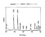
ここで、各結晶系の酸化イットリウムについて説明する。図2はイットリウムが大気酸化されてなる酸化イットリウムの結晶格子のX線回折パターンを、図3はイットリウムが主に水素雰囲気中で酸化されてなる酸化イットリウムの結晶格子の状態を示すX線回折パターンを示している。図2に示した酸化イットリウムは、その格子定数が10.60Åであり、その結晶系は体心立方格子(以下、I型格子という)と指数づけられた。図3に示した酸化イットリウムは、その格子定数が14.85Åであり、その結晶系は単純立方格子(以下、II型格子という)と指数づけられた。図10に示した酸化イットリウムは、その格子定数が5.21Åであり、その結晶系は面心立方格子(以下、III型格子という)と指数付けされた。他に結晶系がI型格子とII型格子との中間型のI−II型格子やII型格子とIII型格子の中間型のII−III型格子があり、これら異なる結晶系の酸化イットリウム膜の厚さ方向の電気抵抗を調べたところ、いずれも電気伝導性が確認された。
【0018】
放電特性では、II型格子の酸化イットリウム膜、II−III型格子の酸化イットリウム膜、III型格子の酸化イットリウム膜を用いた電極が相対的に最も放電電圧が低く、次いでI−II型格子、I型格子の順に低い。このような酸化イットリウムは仕事関数が低く、極めて良好な電子放出特性を有しているため、低電流で効率よく電子を電子輸送層または電子輸送性の発光層に注入することができるので、有機EL素子のカソード電極として用いることにより高い発光効率を実現することができる。また、3000時間以上連続放電を行うことができ、カソード電極の長寿命化を可能にした。
【0019】
上記実施形態では、カソード電極5およびアノード電極8を互いに直交する複数のストライプ形状にした高時分割駆動のドットマトリクス表示にしてもよいし、カソード電極5あるいはアノード電極8の一方を、それぞれ薄膜トランジスタに接続された複数の画素電極とし、他方を共通電極としたアクティブ駆動でもよく、また、カソード電極5およびアノード電極8の少なくとも一方を、文字、図形の形状にして表示を行ってもよい。
【0020】
次に、本実施形態のEL発光素子1の製造方法1〜4について説明する。
(製造方法1)
以下、本実施形態1のEL発光素子1の製造方法1について説明する。この方法によって、電極表面にY2O3-x(xは0.0以上1.0以下である)でなる電子放出性を有する膜が形成できる。まず、基板2を洗浄する。次いで、基板2の表面に、Al膜3をスパッタ法により形成し、その上にイットリウムを例えば抵抗加熱や電子ビームなどの手法を用いて蒸着またはスパッタして、膜厚が500Å〜5000Å程度のイットリウム膜を成膜する。
【0021】
その後、基板2を反応炉内に搬入し、イットリウム膜の表面を酸化処理する。この反応炉は、気体導入路と気体排出路とを備え、所定の流量で水素(H2)ガスが気体導入路から導入され、常に炉内が水素ガスで満たされるように設定されている。なお、この反応炉内には、酸素(O2)および/または酸素含有物の濃度が1体積%以下、望ましくは1000ppm以下、さらに望ましくは100ppm以下存在するように制御されている。酸素含有物としては、例えば水蒸気を用いることができる。なお、酸素および/または酸素含有物の濃度は、気体導入路と気体排出路とに繋がっている酸素を吸着するフィルタおよび水を吸着するフィルタと、炉内に導入される水素濃度を制御することにより予め制御することができる。
【0022】
次に、炉内の温度を常温から600℃程度の温度まで100℃/15分〜100℃/5分の割合で昇温し、600℃程度で10〜60分間加熱する。この酸化処理工程は、300℃以上1000℃以下の範囲、望ましくは500℃以上700℃以下の範囲で行えばよい。また、昇温の割合は、100℃/20分〜100℃/5分の割合であればよい。このようにして、基板2上のイットリウム膜4A表面に酸化イットリウム膜4Bを形成することができる。
【0023】
この後は、脱水素処理工程を行う。すなわち、基板2を減圧雰囲気(1×10⁻³Torr以下、望ましくは1×10⁻⁶Torr以下)中で、350℃以上、望ましくは450℃以上800℃以下で15分間加熱し、イットリウム膜4Aおよび酸化イットリウム膜4B中に含まれている水素を除去する。
【0024】
次に、酸化イットリウム膜4B上にAlq3をディップコートもしくはスピンコートなどの湿式成膜により塗布して電子輸送層6を形成する。その後、電子輸送層6上に、PVCzとBNDとクマリン6との混合物を同じくディップコートもしくはスピンコートなどの湿式成膜により塗布して正孔輸送層7を形成する。その後、正孔輸送層7上にITOでなるアノード電極8を、スパッタ法により形成する。なお、カソード電極5とアノード電極8とは、対向する部分に駆動電圧が印加されることにより発光する領域が形成される訳であるが、この発光領域を画素単位に形成する際には、カソード電極5とアノード電極8とが互いに平面的に見て交差するようなパターン、すなわちカソード電極5とアノード電極8とをそれぞれストライプ状に形成する場合には、両電極が互いに異なる方向に延在されるようにパターニングする工程が必要となることは言うまでもない。また、両電極のうち一方が表示領域全面に亙って形成された平板状の電極で、他方の電極が各画素毎に矩形状または円形状にパターニングされた構成としてもよい。
【0025】
以上、製造方法1について説明したが、上記方法において酸素および/または酸素含有物の濃度を変えると以下に説明するような特徴を有する酸化イットリウムとなる。
【0026】
まず、酸素および/または酸素含有物の濃度が100ppmオーダを越える水素雰囲気下で膜厚3000Å程度のイットリウム膜を加熱酸化すると、図4のX線回折パターンに示されるような4500Å程度のI型格子(体心立方格子)に指数付けされた酸化イットリウム膜が形成される。このI型格子の酸化イットリウム膜は、格子定数が10.60Åであり、図5に示すように29°近傍の強度ピークに特徴がある。
【0027】
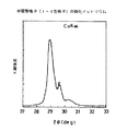
上記製造方法において、酸素および/または酸素含有物の濃度が10ppmオーダ程度の水素雰囲気下で膜厚3000Å程度のイットリウム膜を加熱酸化すると図6のX線回折パターンに示されるような4500Å程度のII型格子と指数付けされた酸化イットリウム膜が形成される。このII型格子の酸化イットリウム膜は、格子定数が14.85Åであり、図7に示すように29°近傍に大きい強度ピークが1つと29.6°近傍に大きい強度ピークが1つあるのが特徴である。
【0028】
上記製造方法において、酸素および/または酸素含有物の濃度が100ppmオーダ程度(II型格子のみの酸化イットリウム膜が形成されるより薄い程度)の水素雰囲気下で膜厚3000Å程度のイットリウム膜を加熱酸化すると、図8のX線回折パターンに示されるような4500Å程度のI型格子とII型格子(単純立方格子)との中間型(I-II型)と指数付けされた酸化イットリウム膜が形成される。このI-II型格子の酸化イットリウム膜は、図9に示すように29°近傍に大きい強度ピークが1つと、その右肩(29.6近傍)に小さい強度ピークが1つあるのが特徴である。
【0029】
上記製造方法において、酸素および/または酸素含有物の濃度が1ppmオーダ程度の水素雰囲気下で膜厚3000Å程度のイットリウム膜を加熱酸化すると、図10のX線回折パターンに示されるような4500Å程度の面心立方格子(以下、III型格子という)と指数付けされた酸化イットリウム膜が形成される。このIII型格子の酸化イットリウム膜は、格子定数が5.21Åであり、図11に示すように29.6°近傍に大きい強度ピークが1つあるのが特徴である。
【0030】
上記製造方法において、酸素および/または酸素含有物の濃度が、III型格子のみの酸化イットリウム膜が形成される濃度より濃く、II型格子のみの酸化イットリウム膜が形成されるより薄い程度の水素雰囲気下で膜厚3000Å程度のイットリウム膜を加熱酸化すると、図12のX線回折パターンに示されるような4500Å程度の、II型格子とIII型格子との中間型(以下、II-III型格子という)と指数付けされた酸化イットリウム膜が形成される。このII-III型格子の酸化イットリウム膜は、29.6°近傍に大きい強度ピークが1つと、その左肩(29°近傍)に小さい強度ピークが1つあるのが特徴である。
【0031】
上記したように、水素雰囲気内の酸素濃度を制御することにより、酸化イットリウム膜の結晶系を制御することができる。上記製造方法により形成された酸化イットリウムからなる電極を、希ガスと水銀が封入された、管径2.6φ、長さ63.5mmの管内に対向して配置して定電流下での放電試験を行なった。III型格子、II-III型格子の管は、いずれも放電電圧が167V、II型格子の管は、172V、I−II型格子、I型格子の管は、それぞれ176V、182Vであった。比較実験としてNi電極を用いた管では、225Vであった。ニッケル電極より大幅に放電電圧が低いということは、これら結晶系の酸化イットリウムのほうが大幅に電子放出性が高いことを示している。因に、ニッケルの仕事関数は5.15eVであるが、これらの結晶系の酸化イットリウムの仕事関数はこの値より大幅に小さいということが確認できる。このため、上記した実施形態1のように、上記結晶系の酸化イットリウム膜をEL発光素子のカソード電極として用いれば、図1に示した電子輸送層6への電子を注入し易くなり、EL発光素子の低消費電力化を達成することができる。また、これらの酸化イットリウムは、放電によるスパッタが少なく、表面を覆うことにより下地である金属のスパッタを抑制できることが確認された。
【0032】
なお、本実施形態では、希土類酸化物を構成する希土類元素としてしては、イットリウムを用いたが、この他に、スカンジウム(Sc)、ランタン(La)、セリウム(Ce)、プラセオジム(Pr)、ネオジム(Nd)、プロメチウム(Pm)、サマリウム(Sm)、ユウロピウム(Eu)、ガドリニウム(Gd)、テルビウム(Tb)、ジスプロシウム(Dy)、ホルミウム(Ho)、エルビウム(Er)、ツリウム(Tm)、イッテルビウム(Yb)、ルテチウム(Lu)の中から選択することができる。また、希土類酸化物は、アノード電極材料より低仕事関数の材料であれば、上記材料に限定されるものではない。
(製造方法2)
以下、本実施形態のEL発光素子1の製造方法2を説明する。この方法においても、電極表面にY2O3-x(xは0.0以上1.0以下である)でなる電子放出性を有する膜が形成できる。
【0033】
まず、基板2を洗浄する。次いで、基板2の表面に、Al膜3をスパッタ法により形成し、その上にイットリウムを例えば抵抗加熱や電子ビームなどの手法を用いて蒸着またはスパッタして、膜厚が500Å〜5000Å程度のイットリウム膜を成膜する。
【0034】
その後、基板2を反応炉内に搬入し、イットリウム膜の表面を酸化処理する。この反応炉は、気体導入路と気体排出路とを備え、所定の流量でアルゴン(Ar)が気体導入路から導入され、常に炉内がアルゴンで満たされるように設定されている。なお、この反応炉内には、酸素(O2)および/または酸素含有物の濃度が1体積%以下、望ましくは1000ppm以下、さらに望ましくは100ppm以下存在するように制御されている。酸素含有物としては、例えば水蒸気が炉内に存在し、また極微量の水素が存在する。なお、酸素および/または酸素含有物の濃度は、気体導入路と気体排出路とに繋がっている酸素を吸着するフィルタおよび水を吸着するフィルタと、炉内に導入されるアルゴン濃度を制御することにより予め制御することができる。
【0035】
次に、アルゴン雰囲気で炉内の温度を常温から600℃程度の温度まで100℃/15分〜100℃/5分の割合で昇温し、600℃程度で10〜60分加熱する。この酸化処理工程は、300℃以上1000℃以下の範囲、望ましくは500℃以上700℃以下の範囲で行えばよい。また、昇温の割合は、100℃/20分〜100℃/5分の割合であればよい。このようにして、基板2上のイットリウム膜4A表面に酸化イットリウム膜4Bを形成することができる。
【0036】
このように形成された酸化イットリウム膜の結晶系は、実質的に上記した製造方法1と同様であり、酸素および/または酸素含有物の濃度に応じて制御することができ、I型格子、I-II型格子、II型格子の酸化イットリウム膜の生成が確認できた。この製造方法2では、上記製造方法1が水素雰囲気でイットリウム膜を参加しているのに対し、アルゴン雰囲気下で酸化が行われている点で異なる。また、この製造方法2では、アルゴン雰囲気下で酸化が行われているので基板2、Al膜3、イットリウム膜内に水素が実質的に混入されていなければ、生成された酸化イットリウム膜内に水素がほとんど混入されず、脱水素処理を施す必要がない。このため、上記製造方法1に比較して工程数が少なくてすむ。ただし、基板2、Al膜3、イットリウム膜のいずれかに水素が含まれている場合は、脱水素処理を必要とする。また、電子輸送層6、正孔輸送層7、アノード電極8などの形成方法は、上記した製造方法1と同様である。
【0037】
(製造方法3)
以下、本実施形態のEL発光素子1の製造方法3を説明する。この方法においても、電極表面にY2O3-x(xは0.0以上1.0以下である)でなる電子放出性を有する膜が形成できる。
【0038】
まず、基板2を洗浄する。次いで、基板2の表面に、Al膜3をスパッタ法により形成し、その上にイットリウムを例えば抵抗加熱や電子ビームなどの手法を用いて蒸着またはスパッタして、膜厚が20000Å〜40000Å程度のイットリウム膜を成膜する。次に、イットリウム膜の上に、アモルファス状の酸化イットリウム膜を、イオンプレーティング法により500〜2000Å程度の膜厚に成膜する。
【0039】
その後、基板2を反応炉内に搬入し、イットリウム膜の表面を酸化処理する。この反応炉は、気体導入路と気体排出路とを備え、所定の流量で水素(H2)ガスが気体導入路から導入され、常に炉内が水素ガスで満たされるように設定されている。なお、この反応炉内には、酸素(O2)および/または酸素含有物の濃度が1体積%以下、望ましくは1000ppm以下、さらに望ましくは100ppm以下存在するように制御されている。なお、酸素含有物としては、例えば水蒸気を用いることができる。なお、酸素および/または酸素含有物の濃度は、気体導入路と気体排出路とに繋がっている酸素を吸着するフィルタおよび水を吸着するフィルタと、炉内に導入される水素濃度を制御することにより予め制御することができる。
【0040】
次に、炉内の温度を常温から600℃程度の温度まで100℃/15分〜100℃/5分の割合で昇温させ、600℃程度で10〜60分間加熱する。この酸化処理工程は、300℃以上1000℃以下の範囲、望ましくは500℃以上700℃以下の範囲で行えばよい。また、昇温の割合は、100℃/20分〜100℃/5分の割合であればよい。このようにして、基板2上のイットリウム膜4A表面に酸化イットリウム膜4Bを形成することができる。
【0041】
この後は、脱水素処理工程を行う。すなわち、基板2を減圧雰囲気(1×10⁻³Torr以下、望ましくは1×10⁻⁶Torr以下)中で、350℃以上、望ましくは450℃以上800℃以下で15分間加熱し、酸化イットリウム膜4B内に含まれている水素を除去する。また、電子輸送層6、正孔輸送層7、アノード電極8などの形成方法は、上記した製造方法1と同様である。
【0042】
このような製造方法3によって、I型格子、I-II型格子、II型格子の酸化イットリウム膜の生成が確認された。
【0043】
(製造方法4)
以下、本実施形態のEL発光素子1の製造方法4を説明する。この方法においても、電極表面にY2O3-x(xは0.0以上1.0以下である)でなる電子放出性を有する膜が形成できる。
【0044】
まず、基板2を洗浄する。次いで、基板2の表面に、Al膜3をスパッタ法により形成し、その上にイットリウムを例えば抵抗加熱や電子ビームなどの手法を用いて蒸着またはスパッタして、膜厚が20000Å〜40000Å程度のイットリウム膜を成膜する。次に、イットリウム膜の上に、アモルファス状の酸化イットリウム膜を、イオンプレーティング法により500〜2000Å程度の膜厚に成膜する。
【0045】
その後、基板2を反応炉内に搬入し、酸化処理を施す。この反応炉は、気体導入路と気体排出路とを備え、所定の流量でアルゴン(Ar)が気体導入路から導入され、常に炉内がアルゴンで満たされるように設定されている。なお、この反応炉内には、酸素(O2)および/または酸素含有物の濃度が1体積%以下、望ましくは1000ppm以下、さらに望ましくは100ppm以下存在するように制御されている。酸素含有物としては、例えば水蒸気が炉内に存在する。なお、酸素および/または酸素含有物の濃度は、気体導入路と気体排出路とに繋がっている酸素を吸着するフィルタおよび水を吸着するフィルタと、炉内に導入されるアルゴン濃度を制御することにより予め制御することができる。
【0046】
次に、アルゴン雰囲気で炉内の温度を常温から600℃程度の温度まで100℃/15分〜100℃/5分の割合で昇温し、600℃程度で10〜60分間加熱する。この酸化処理工程は、300℃以上1000℃以下の範囲、望ましくは500℃以上700℃以下の範囲で行えばよい。また、昇温の割合は、100℃/20分〜100℃/5分の割合であればよい。このようにして、基板2上のイットリウム膜4A表面に所定結晶系の酸化イットリウム膜4Bを形成することができる。なお、電子輸送層6、正孔輸送層7、アノード電極8などの形成方法は、上記した製造方法1と同様である。
【0047】
なお、この製造方法4では、アルゴン雰囲気下で酸化を行っているため、基板2、Al膜3、イットリウム膜内に水素が実質的に混入されていなければ、生成された酸化イットリウム膜内に水素がほとんど混入されない。このため、脱水素処理を施す必要がなく、工程数を製造方法1に比較して少なくすることができる。ただし、基板2、Al膜、イットリウム膜のいずれかに水素が含まれている場合は、脱水素処理を行うことが望ましい。このように形成された酸化イットリウム膜の結晶系は、酸素および/または酸素含有物の濃度に応じて制御することができ、I型格子、I-II型格子、II型格子の酸化イットリウム膜の生成が確認できた。なお、イオンプレーティング法で成膜された酸化イットリウム膜の酸化前の膜厚が1000Å程度の場合、酸素濃度が100ppmオーダでI型格子、10ppmオーダでII型格子の酸化イットリウムの生成が確認された。
【0048】
本実施形態のEL発光素子1では、カソード電極5の表面に形成された酸化イットリウム膜4Bの電気抵抗が、数十Ω以下と小さく、電気伝導性を示している。これに加えて、酸化イットリウムは、その仕事関数が小さく、高い電子放出性を有する。酸化イットリウムは、このような特性を持つため良好なカソード電極として用いることができる。このため、本実施形態のEL発光素子は、発光電圧の低い低消費電力な駆動を行うことができる。また、酸化イットリウム自体が、化学的に安定な物質であるため、電極の寿命を長くすると共に、素子自体の寿命を長くすることができる。なお、本実施形態では、電子輸送層としてAlq3を、正孔輸送層としてPVCzとBNDを混合したものを用いたが、この他各種のEL材料を適用することができる。また、EL層の構造も2層構造に限定されるものではなく、電子輸送層と正孔輸送層との間に発光層を設けた3層構造でもよい。
【0049】
図17に示すように、4500Å程度のI型格子の酸化イットリウム膜では可視光波長域での透過性は概ね50%を超えており、基板2、Al膜3、イットリウム膜4Aの厚さ等を制御して可視光波長域において透過性を持たせれば、I型格子のEL発光素子1の発光を基板2側から出射することができる。
【0050】
イットリウム膜4Aは、酸化イットリウム4Bを生成する際にAl膜3の酸化による電気的絶縁を防止するとともに各層間の接合性を良好にするものであるが、このような中間層はイットリウムに限ることなく、所定の仕事関数であれば他の導電性材料でもよい。
【0051】
以上、実施形態1に係るEL発光素子とその製造方法1〜4について説明したが、次に、実施形態2に係るEL発光素子について以下に説明する。
【0052】
(実施形態2)
図13は、本発明をEL発光素子に適用した実施形態2の断面図である。本実施形態においては、基板2上にAl膜3が形成され、このAl膜3の上に酸化イットリウム膜4Bが形成され、酸化イットリウム膜4Bの上に順次、電子輸送層6、正孔輸送層7、アノード電極8が形成された構成となっている。なお、他の構成は、上記した実施形態1と同様である。
【0053】
次に、本実施形態のEL発光素子1の製造方法を説明する。この方法においても、電極表面にY2O3-x(xは0.0以上1.0以下である)でなる電子放出性を有する膜が形成できる点では、上記した製造方法1および2と同様であるが、この製造方法ではAl膜3上に直接、酸化イットリウム膜を形成する点で異なる。
【0054】
まず、基板2を洗浄する。次いで、基板2の表面にAl膜3をスパッタ法により形成し、その上にイオンプレーティングによりアモルファス状の酸化イットリウム膜を、膜厚が1000Å〜5000Å程度になるように成膜する。
【0055】
その後、基板2を反応炉内に搬入する。この反応炉は、気体導入路と気体排出路とを備え、所定の流量で水素(H2)ガスが気体導入路から導入され、常に炉内が水素ガスで満たされるように設定されている。なお、この反応炉内には、酸素(O2)および/または酸素含有物の濃度が1体積%以下、望ましくは1000ppm以下、さらに望ましくは100ppm以下存在するように制御されている。酸素含有物としては、例えば水蒸気を用いることができる。なお、酸素および/または酸素含有物の濃度は、気体導入路と気体排出路とに繋がっている酸素を吸着するフィルタおよび水を吸着するフィルタと、炉内に導入される水素濃度を制御することにより予め制御することができる。
【0056】
次に、炉内の温度を常温から600℃程度の温度まで100℃/15分〜100℃/5分の割合で昇温し、600℃程度で10〜60分加熱する。この酸化処理工程は、300℃以上1000℃以下の範囲、望ましくは500℃以上700℃以下の範囲で行えばよい。また、昇温の割合は、100℃/20分〜100℃/5分の割合であればよい。このようにして、基板2表面に酸化イットリウム膜を形成することができる。
【0057】
この後は、脱水素処理工程を行う。すなわち、基板2を減圧雰囲気(1×10⁻³Torr以下、望ましくは1×10⁻⁶Torr以下)中で、350℃以上、望ましくは450℃以上800℃以下で15分間加熱し、酸化イットリウム膜中に含まれている水素を除去する。また、電子輸送層6、正孔輸送層7、アノード電極8などの形成方法は、上記した製造方法1と同様である。
【0058】
このような製造方法によって、I型格子、I-II型格子、II型格子の酸化イットリウム膜の生成が確認された。本実施形態のEL発光素子においても、上記した実施形態1のEL発光素子と同様に、カソード電極5の表面に形成された、上記の結晶系をもつ酸化イットリウム膜4Bの電気抵抗が、数十Ω以下と小さく、電気伝導性を示している。これに加えて、酸化イットリウムは、その仕事関数が小さく、高い電子放出性を有する。酸化イットリウムは、このような特性を持つため良好なカソード電極として用いることができる。このため、本実施形態のEL発光素子は、発光電圧を低い低消費電力な駆動を行うことができる。また、酸化イットリウム自体が、化学的に安定な物質であるため、電極の寿命を長くすると共に、素子自体の寿命を長くすることができる。
【0059】
(実施形態3)
図14は、本発明をEL発光素子に適用した実施形態3の断面図である。本実施形態においては、上記実施形態1のカソード電極5を構成するAl膜3を、ITO膜9に代えたものであり、他の構成、作用、効果は上記実施形態1と同様である。また、ITO膜9上にイットリウム膜4Aと酸化イットリウム膜4Bとを形成する方法も上記実施形態1と同様である。
【0060】
(実施形態4)
以下、アドレス信号光を発生させるアドレス発光部と、表示光を発生させる表示部と、を有する発光表示素子に、本発明を適用した実施形態4について説明する。図15は、実施形態4の発光表示素子の断面図である。同図中11は、発光表示素子である。この発光表示素子11は、表示部12と、アドレス発光部13と、から大略構成されている。
【0061】
表示部12は、例えばシリカガラス或いは合成樹脂などの透明基板14の裏面に、表示領域全面に亙って、順次ITO膜15、酸化イットリウム膜16が積層されている。これらITO膜15と酸化イットリウム膜16とが、表示駆動用カソード電極17を構成している。この表示駆動用カソード電極17の形成方法は、透明基板14上にITO膜15を形成した後、上記した実施形態2と同様の方法を用いて形成することができる。なお、本実施形態において酸化イットリウム膜16の結晶系は、特に光透過性の良好な上記したI型格子(体心立方格子)のものを用いる。
【0062】
次に、酸化イットリウム膜16上(裏面)には、表示領域全面に亙って、順次、Alq3でなる電子輸送層18、PVCzとBNDとを混合してなる正孔輸送層19が周知の方法で形成されている。なお、発光領域である正孔輸送層19の各ドット部分には、電子と正孔の再結合により発光する光を吸収し、それぞれR(レッド)、G(グリーン)、B(ブルー)に発光する蛍光材料を含有するように形成すれば、多色表示が可能となる。正孔輸送層19の上(裏面)には、アモルファスシリコン(a−Si)にn型不純物(例えば、リン)をドープしてなるドープ層20が表示領域全面に亙って形成されている。また、ドープ層20の上(裏面)には、アモルファスシリコンでなる光導電層21が表示領域全面に亙って形成されている。なお、ドープ層20と光導電層21は、後記するアドレス発光部13側から照射される白色光(アドレス光)が入射した部分だけに内部に電子−正孔対を生成し、導電性を示すようになる。そして、光導電層21の上(裏面)には、所定方向に平行に並ぶ複数の表示駆動用アノード電極22がストライプ状に形成されている。なお、この表示駆動用アノード電極22の材料としては、後記するアドレス光に対して透明性をもつITOが用いられている。上記したITO膜15から表示駆動用アノード電極22までの部材により、表示部12が構成されている。
【0063】
表示駆動用アノード電極22が形成された光導電層21の上(裏面)には、例えばシリコン窒化膜やシリコン酸化膜でなる、平坦化絶縁膜23が周知の平坦化技術を用いて形成されている。そして、この平坦化絶縁膜23の上(裏面)には、表示駆動用アノード電極22と対向して平面的に重なるように、表示駆動用アノード電極22と同じ本数のアドレス駆動用カソード電極24が形成されている。このアドレス駆動用カソード電極24は、ITOでなる電極基体25の表面に薄い膜厚の酸化イットリウム膜26が形成されて構成されている。なお、酸化イットリウム膜26の結晶系は、上記した表示駆動用カソード電極17の酸化イットリウム膜16と同様に、光透過性の良好なI型格子(体心立方格子)のものを用いる。
【0064】
そして、アドレス駆動用カソード電極24が形成された平坦化絶縁膜23の上(裏面)にはAlq3でなる電子輸送層27、PVCzとBNDと白色発光材料とを混合してなる正孔輸送層28が周知の技術で順次積層するように形成されている。さらに、正孔輸送層28の裏面には、ITOでなる、複数のアドレス駆動用アノード電極29が、上記したアドレス駆動用カソード電極24と平面的に見て交差するように、ストライプ状に形成されている。
【0065】
以下、本実施形態の発光表示素子11の作用・動作を説明する。
まず、アドレス発光部13において、線順次走査により選択されたアドレス駆動用カソード電極24とアドレス駆動用アノード電極29との間に所定電圧が印加されると、電子輸送層27と正孔輸送層28との界面近傍で電子と正孔との再結合が起こり、図15に示すようにアドレス光(白色光)aが光導電層21およびドープ層20に向けて出射する。なお、このとき、電子輸送層27と正孔輸送層28との界面と、光導電層21およびドープ層20と、の距離は、実際には十分に近い距離(アドレス光が空間周波数を維持して入射し得る距離)であるため、対応する領域の光導電層21およびドープ層20のみに入射する。このため、所定のアドレスから発光するアドレス光が、隣接するドット部分の光導電層21およびドープ層20に入射してその領域に電子−正孔対を生成することはない。電子−正孔対が生成された光導電層21およびドープ層20を介することにより、表示駆動用アノード電極22から正孔輸送層19へ正孔を注入することが可能となる。これによって、表示駆動用アノード電極22と表示駆動用カソード電極17との間に印加されていた表示駆動電圧は、正孔輸送層19と電子輸送層18とでなる有機EL層の対応するドット部分に印加される。なお、表示駆動用の電極間には、直流駆動電圧、パルス電圧、交流電圧などを用いることができる。この結果、表示部12の発光により図15に示すように表示光bが前方に向けて照射され、表示を行うことができる。
【0066】
特に、本実施形態の発光表示素子11においては、上記したように、表示駆動用カソード電極17およびアドレス駆動用カソード電極24の表面層が酸化イットリウム膜16、26で構成されている。酸化イットリウム膜は、その電気抵抗が、上記したように数十Ω以下と小さく電気伝導性をもち、これに加えて、仕事関数が十分小さいため、高い電子放出性を有する。このため、本実施形態の発光表示素子11は、表示部12およびアドレス発光部13において、発光電圧を低くすることができ、低消費電力な駆動を行うことができる。また、酸化イットリウム自体が、化学的に安定な物質であるため、従来からの課題であるカソード電極の寿命を長くすると共に、素子自体の寿命を長くすることができる。
【0067】
次に、上記した発光表示素子11における各構成部材の光透過性について説明する。透明基板14、ITO膜15、電子輸送層18は、表示光(可視光)bに対して良好な光透過性をもつ。また、表示駆動用アノード電極22、平坦化絶縁膜23、電極基体25、電子輸送層27は、アドレス光(可視光)に対して透過性をもつ。そこで、酸化イットリウム膜16の表示光bに対する透過性と、酸化イットリウム膜26のアドレス光aに対する透過性が重要となる。
【0068】
ここで、酸化イットリウムの光学的特性について説明する。まず、石英基板上に電子ビーム蒸着により成膜された膜厚3000Å程度のイットリウム膜を所定濃度の水素雰囲気下で600℃程度の温度で15分間加熱して得られた酸化イットリウム膜と、石英基板上に電子ビーム蒸着により成膜された膜厚3000Å程度のイットリウム膜を大気中で700℃程度の温度で30分間加熱して得られた酸化イットリウム膜を用意した。
【0069】
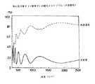
上記した所定濃度の水素雰囲気下で酸化された酸化イットリウムは、上記したII型格子であり、石英基板上の酸化イットリウムの光透過特性を図16に示す。光透過率は、石英および酸化イットリウムのいずれも介さない光の光量を100とした場合の、石英および酸化イットリウムを透過した光の光量の相対的な割合である。光反射率は、所定の光量の光に対して表面が平滑なアルミニウム(Al)板の反射光量を100とした場合の、石英および酸化イットリウムで反射された光の光量の相対的な割合ある。
【0070】
大気酸化された酸化イットリウムはI型格子であり、その光透過特性を図17に示す。図17に示すI型格子の酸化イットリウム膜の場合は、光透過率が波長が500nm〜2500nmの範囲において常に50%を越えている。これに対して、図16に示したII型格子の酸化イットリウム膜の場合は、光透過率が波長500nm〜2500nmの範囲において常に20%より低い。また、I型格子の酸化イットリウム膜の場合には、光反射率が波長500nm〜2500nmの範囲で常に40%以下である。これに対しII型格子の酸化イットリウム膜の場合には、光反射率が波長500nm〜2500nmの範囲において数%〜75%の間で変化しており、最大反射率は60%を越えている。このように異なる結晶系の酸化イットリウムどうしは、光学的特性が大きく異なることがわかる。このことから、本実施形態の発光表示素子11のカソードとしては、I型格子の酸化イットリウムを用いることで、アドレス光aや表示光bの光利用効率を向上できることがわかる。
【0071】
次に、物質固有の光学的指標の1つとして吸収端(absorption edge)について、上記I型格子およびII型格子の酸化イットリウムについて調べてみた。吸収端は、一般的にX線または光の連続吸収スペクトルにおいて、波長がこれ以上長くなると吸収率が急激に減少するようになる部分またはその端のことをいう。ここでは、吸収端を光透過率が測定不可となる値まで落ち込んだところと定義する。図18は、所定濃度の水素雰囲気下で酸化されたII型格子の酸化イットリウムの吸収端を示している。図19は、大気中で酸化されたI型格子の酸化イットリウムの吸収端を示している。図19に示した酸化イットリウムでは、約5.9eVであるのに対し、図18に示した酸化イットリウムでは、4.0eV以下になっている。このことからII型格子の酸化イットリウムがI型格子の酸化イットリウムに比べ低エネルギー側にシフトしていることがわかる。以上のことから、酸化イットリウムでは、その結晶系に応じて様々な光学的特性が異なることがわかる。
【0072】
上記各実施形態では、正孔輸送層および電子輸送層で再結合による発光を表示光として用いてもよいし、再結合による発光を吸収してより長波長域の可視光を発光してもよい。
【0073】
また実施形態4では、光導電層21に、可視光に光吸収性がなく紫外線に光吸収性があるZnO(酸化亜鉛)を用い、正孔輸送層19にはPVCzとBNDとの混合物、電子輸送層18にはAlq3を用いれば、アドレス発光部13から紫外線の発光させ、紫外線が照射されない状態では絶縁性であった光導電層21がアドレス発光部13からの紫外線の波長域の光を吸収することにより厚さ方向に導電性をもたらすことができる。この作用に従って、予め表示駆動用カソード電極17および表示駆動用アノード電極22間に印加される電圧により、表示駆動用アノード電極22から光導電層21およびドープ層20を介して正孔輸送層19に正孔が注入され、表示駆動用カソード電極17から電子輸送層18に電子が注入され、表示部12で再結合を行ない、表示光bが照射される。このように光導電層21が紫外線の波長域のみで導電性をもたらすよう設定されているので、表示部12にアドレス光以外の可視光が入射したとしても誤動作が発生することはない。
【0074】
(実施形態5)
図20は、本発明をPDPに適用した実施形態5を示す断面図である。本実施形態のPDPは、直流駆動のカラーPDPである。同図中91はPDPであり、それぞれ赤色、緑色、青色を表示する複数の画素から構成されている。各画素は、透明な上基板92と下基板93との間に設けられた格子状あるいはストライプ状の障壁101により区分けされている。下基板93上には、補助カソード電極94が各画素の中央に配置されている。補助カソード電極94は、ニッケル(Ni)、クロム(Cr)、アルミニウム(Al)、マンガン(Mo)の中から少なくとも1つ選択される導体からなる基体95と、基体95上に形成された希土類酸化物層としての酸化イットリウム膜96と、から構成されている。補助カソード電極94の周囲には、データ電極97が電極94と離間して配置されている。補助カソード電極94を中心としたデータ電極97の外側方向にはアモルファスシリコンなどでなる電流制御膜98が配置されている。また、電流制御膜98のさらに外側にはカソード電極102が配置されている。カソード電極102は、Ni、Cr、Al、Moの中から少なくとも1つ選択される導体からなる基体103と、基体103上に形成された希土類酸化物層としての酸化イットリウム膜104と、から構成されている。この電流制御膜98は、データ電極97からの電流のふらつきを抑制している。電流制御膜98の抵抗は、膜厚、長さ、アモルファスシリコン中に添加される不純物などにより設定することができる。
【0075】
また、下基板93上には、補助カソード電極94の酸化イットリウム膜96とカソード電極102の酸化イットリウム膜104を除く全面に絶縁膜105が設けられている。補助カソード電極94の周囲の絶縁膜105上には、補助障壁106が形成されている。障壁101および補助障壁106は、各画素毎に、赤色に発光する蛍光体107R、緑色に発光する蛍光体107G、青色に発光する蛍光体107Bがそれぞれ設けられている。蛍光体107Rとしては、(Y,Gd)BO3:Eu3+:Y2O3:Eu3+があり、蛍光体107Gとしては、Zn2SiO4:Mn,BaAl12O19:Mnがあり、蛍光体107Bとしては、BaMgAl14O23:Eu2+,SrMg(SiO4)2:Eu2+がある。
【0076】
上基板92には、各画素に応じて、赤色に分光するカラーフィルタ111R、緑色に分光するカラーフィルタ111G、青色に分光するカラーフィルタ111Bが設けられている。カラーフィルタ111R、111G、111Bの表面には、ITOからなる透明電極112が設けられている。また、上基板92と下基板93と障壁101に囲まれた空間には、ヘリウム(He)、キセノン(Xe)を含む希ガス113が封入されている。
【0077】
上記した構成のPDP91においては、カソード側の表面層に酸化イットリウム膜104が形成されているため、電子放出性を大幅に向上させ、PDPの低消費電力化を達成することができる。酸化イットリウム膜96、104は、結晶系として、I型格子、I−II型格子、II型格子、II−III型格子、III型格子があるが、放電特性の観点からは、II−III型格子、III型格子が最も好ましく、次いでII型格子、I−II型格子、I型格子の順によく、いずれも発光輝度の高い表示を行なうことができる。また、本実施形態では、カソード電極の一部として耐スパッタ性に優れている酸化イットリウムが電極94、102の基体95、103を覆うように形成されているので酸化イットリウム膜128のみならず基体95、103のスパッタも抑制することができ、画素内のスパッタによる汚染や電子放出性の経時的な逓減にともなう発光輝度の低下を抑制することができる。
【0078】
次に、上記したPDP91の駆動方法について説明する。第1に、透明電極112と補助カソード電極94との間に所定の電圧を印加することにより補助プラズマを発生させる。第2に、各画素には表示に応じたデータ電圧がデータ電極97に印加され、電流制御膜98から制御された電流がカソード電極102に流れる。カソード電極102と透明電極112との間には、補助プラズマの補助により、プラズマがすばやく発生する。このプラズマにより希ガスからの紫外線が発生し、紫外線が各画素の蛍光体に当たり、所定の波長域の光を発光し、上基板92を透過して表示される。
【0078】
また、外光がPDP91に入射すると、カラーフィルタ111R、111G、111Bにより各色に分光されて上基板92から出射されるので、蛍光体107R、107G、107Bの発光に加え、より色相の濃い色で表示することができる。また、カラーフィルタ111R、111G、111Bは分光しているので、外光の反射によるちらつきを抑制することができ、見やすい表示が可能となる。
【0079】
なお、上記したPDP91は、蛍光体を用いたカラー発光であったが、蛍光体を用いずにプラズマ発光による橙色を表示色に用いるPDPにも本発明をできることは言うまでもない。
【0080】
上記PDP91に用いる希土類酸化物を構成する希土類元素としてしては、イットリウムの他に、スカンジウム(Sc)、ランタン(La)、セリウム(Ce)、プラセオジム(Pr)、ネオジム(Nd)、プロメチウム(Pm)、サマリウム(Sm)、ユウロピウム(Eu)、ガドリニウム(Gd)、テルビウム(Tb)、ジスプロシウム(Dy)、ホルミウム(Ho)、エルビウム(Er)、ツリウム(Tm)、イッテルビウム(Yb)、ルテチウム(Lu)の中から選択することができる。また、基体95、103は、アノード電極である透明電極112より低仕事関数の材料であれば、上記材料に限定されるものではない。
【0081】
(実施形態6)
図21は、本発明をFEDに適用した実施形態6の断面図である。同図中121はFEDであり、それぞれ赤色、緑色、青色を表示する複数の画素から構成され、各画素は、互いに離間して配置された透明な上基板122と下基板123との間に格子状あるいはストライプ状の障壁により区分けされている。下基板123上には、輝度データ電圧が印加されるデータ電極124が設けられ、そのデータ電極124の上には、アモルファスシリコンからなる電流制御膜125が形成されている。電流制御膜125の上には、1画素につき、約2000程度の数の円錐状のカソード電極126が設けられている。カソード電極126は、円錐状のNi、Cr、Al、Moの中から少なくとも1つ選択される基体127と、その表面に形成された酸化イットリウム膜128と、から構成されている。各カソード電極126は、隣接するカソード電極126と絶縁膜129を介している。絶縁膜129上には、カソード電極126上が解放しているゲート電極130が設けられている。この電流制御膜125は、データ電極124からの電流のふらつきを抑制するため、電流を制限している。電流制御膜125の抵抗は、膜厚、長さ、アモルファスシリコン中に添加される不純物などにより設定することができる。
【0082】
上基板122には、カソード電極126と対向面にITOからなるアノード電極の透明電極131が設けられており、透明電極131の表面には、赤色に発光する蛍光体132R、緑色に発光する蛍光体132G、青色に発光する蛍光体132Bがそれぞれ設けられている。
【0083】
次に、本実施形態のFEDの駆動方法について説明する。
まず、透明電極131おデータ電極124との間に各画素の応じたデータ電圧が印加される。データ電極124からは、電流制御膜125を介して制御された電流がカソード電極126の基体127に流れる。色表示する画素のゲート電極130には選択電圧が印加され、ゲート電極130により選択されたカソード電極126は、データ電圧に応じてカソード電極126の先端の酸化イットリウム膜128から電子が放出される。
【0084】
放出された電子は、所定の電圧が印加された透明電極131の方に寄せられている。このため、電子は透明電極131の表面にある蛍光体132R、132G、132Bに当たり、蛍光体132R、132G、132Bが可視光を発光して、可視光が透明基板122を透過してカラー表示される。なお、本実施形態ではカラー表示を行うFEDの構成について説明したが、単色表示を行う構成としても勿論よい。
酸化イットリウム膜128は、結晶系として、I型格子、I−II型格子、II型格子、II−III型格子、III型格子があるが、放電特性の観点からは、II−III型格子、III型格子が最も好ましく、次いでII型格子、I−II型格子、I型格子の順によく、いずれも発光輝度の高い表示を行なうことができる。また、FED121は、上基板122と下基板123との間の空間は電子の授受を良好に行なうために減圧雰囲気下にあり、このため放電による電極のスパッタが著しい装置であるが、本実施形態では、カソード電極の一部として耐スパッタ性に優れている酸化イットリウムが基体127を覆うように形成されているので酸化イットリウム膜128のみならず基体127のスパッタも抑制することができ、画素内のスパッタによる汚染や電子放出性の経時的な逓減にともなう発光輝度の低下を抑制することができる。
【0085】
以上、本実施形態では酸化イットリウム膜を用いて電子放出性の向上を図ったFEDについて説明したが、希土類酸化物を構成する希土類元素としてイットリウムの他に、スカンジウム(Sc)、ランタン(La)、セリウム(Ce)、プラセオジム(Pr)、ネオジム(Nd)、プロメチウム(Pm)、サマリウム(Sm)、ユウロピウム(Eu)、ガドリニウム(Gd)、テルビウム(Tb)、ジスプロシウム(Dy)、ホルミウム(Ho)、エルビウム(Er)、ツリウム(Tm)、イッテルビウム(Yb)、ルテチウム(Lu)の中から選択することができる。
【0086】
また、上記した実施形態6においては、円錐状のNi、Cr、Al、Moの中から少なくとも1つ選択される材料でなる基体127の表面に酸化イットリウム膜128を形成した構成であるが、円錐状の酸化イットリウムのみを電流制御膜125の上に直接形成しても同様の効果を得ることが可能である。このような構成のカソード電極126を形成するには、図22に示すような形成方法を用いればよい。すなわち、図22(a)に示すように、下基板123の上にメタルでなるデータ電極124をパターニングする。さらに、データ電極124の上にアモルファスシリコン膜でなる電流制御膜125を形成する。その後、全面に酸化イットリウム膜128を形成する。なお、酸化イットリウム膜の形成方法は、例えばイオンプレーティングによりアモルファス状の酸化イットリウム膜を形成して水素雰囲気下で酸化処理を行う。その後、酸化イットリウム膜128上にフォトレジスト140を塗布して、露光・現像を行って図22(a)に示すようなパターンを形成する。次に、下地のアモルファスシリコン膜と選択比のとれるエッチング液を用いて酸化イットリウム膜128を等方性エッチングする。すると、図22(b)に示すように略円錐状の酸化イットリウム膜128が形成できる。これを用いて下基板123側を形成することができる。
【0087】
なお、上記した本実施形態においては、メタルでなる基体127の表面に酸化イットリウム膜128を形成した構成であるが、基体127の表面に、順次イットリウム膜、酸化イットリウム膜を形成した構成としても勿論よい。
【0088】
以上、実施形態1〜6について説明したが、希土類酸化物としては、上記したもの他に、希土類を含むペロブスカイト酸化物をカソード電極の表面に用いることができる。希土類を含むペロブスカイト酸化物としては、例えば、La1-xSrxMnO3-y、Nd1-xSrxMnO3-y、La1-xCaxMnO3-y、Nd1-xCaxMnO3-y、Nd1-xPdxMnO3-y、(LaNd)1-xSrxMnO3-y、(LaNd)1-xCaxMnO3-y、(0≦x<0.5、y≧0)などを用いることができる。
【0089】
【発明の効果】
以上の説明から明らかなように、この発明によれば、カソード電極の電子放出性が向上すると共に、耐久性を向上させることができる。このため、低消費電力で寿命の長い発光表示素子を実現することができる。
【図面の簡単な説明】
【図1】本発明をEL発光素子に適用した実施形態1を示す断面図。
【図2】イットリウムが大気酸化されてなる酸化イットリウムの結晶格子のX線回折パターンを示すグラフ。
【図3】イットリウムが主に水素雰囲気中で酸化されてなる酸化イットリウムの結晶格子の状態を示すX線回折パターンを示すグラフ。
【図4】酸素および/または酸素含有物の濃度が100ppmオーダを越える水素雰囲気下でイットリウム膜を加熱酸化して形成された酸化イットリウムのX線回折パターンを示すグラフ。
【図5】酸素および/または酸素含有物の濃度が100ppmオーダを越える水素雰囲気下でイットリウム膜を加熱酸化して形成された酸化イットリウムのX線強度を示すグラフ。
【図6】酸素および/または酸素含有物の濃度が10ppmオーダ程度の水素雰囲気下でイットリウム膜を加熱酸化して形成された酸化イットリウムのX線回折パターンを示すグラフ。
【図7】酸素および/または酸素含有物の濃度が10ppmオーダ程度の水素雰囲気下でイットリウム膜を加熱酸化して形成された酸化イットリウムのX線強度を示すグラフ。
【図8】酸素および/または酸素含有物の濃度が100ppmオーダ程度の水素雰囲気下でイットリウム膜を加熱酸化して形成された酸化イットリウムのX線回折パターンを示すグラフ。
【図9】酸素および/または酸素含有物の濃度が100ppmオーダ程度の水素雰囲気下でイットリウム膜を加熱酸化して形成された酸化イットリウムのX線強度を示すグラフ。
【図10】酸素および/または酸素含有物の濃度が1ppmオーダ程度の水素雰囲気下でイットリウム膜を加熱酸化して形成された酸化イットリウムのX線回折パターンを示すグラフ。
【図11】酸素および/または酸素含有物の濃度が1ppmオーダ程度の水素雰囲気下でイットリウム膜を加熱酸化して形成された酸化イットリウムのX線強度を示すグラフ。
【図12】酸素および/または酸素含有物の濃度が、III型格子のみの酸化イットリウム膜が形成される濃度より濃く、II型格子のみの酸化イットリウム膜が形成されるより薄い程度の水素雰囲気下でイットリウム膜を加熱酸化して形成された酸化イットリウムのX線回折パターンを示すグラフ。
【図13】本発明をEL発光素子に適用した実施形態2を示す断面図。
【図14】本発明をEL発光素子に適用した実施形態3を示す断面図。
【図15】本発明に係る発光表示素子の実施形態4を示す断面図。
【図16】 II型格子の結晶系をもつ酸化イットリウムの光透過特性を示すグラフ。
【図17】I型格子の結晶系をもつ酸化イットリウムの光透過特性を示すグラフ。
【図18】水素雰囲気下で酸化されたII型格子の酸化イットリウムの吸収端を示すグラフ。
【図19】大気中で酸化されたI型格子の酸化イットリウムの吸収端を示すグラフ。
【図20】本発明をPDPに適用した実施形態5を示す断面図。
【図21】本発明をFEDに適用した実施形態6を示す断面図。
【図22】(a)および(b)はFEDのカソード電極の形成方法を示す工程断面図。
【符号の説明】
1 EL発光素子
3 Al膜
4A イットリウム膜
4B 酸化イットリウム膜
5 カソード電極
6 電子輸送層
7 正孔輸送層
8 アノード電極
9 ITO膜
11 発光表示素子
16 酸化イットリウム膜
26 酸化イットリウム膜
104 酸化イットリウム膜
128 酸化イットリウム膜[0001]
BACKGROUND OF THE INVENTION
The present invention relates to a light-emitting display element, and more particularly to a display element that performs self-emission, such as an EL (electroluminescence) display element, a field emission display (hereinafter referred to as FED), and a plasma display panel (hereinafter referred to as PDP).
[0002]
[Prior art]
Conventionally, display elements that emit light include CRT (cathode-ray tube), EL display elements, FED, and PDP. In particular, EL display elements, FEDs, and PDPs have been actively improved because they may achieve thinness, light weight, and low power consumption. In particular, in the EL display element, in recent years, an organic EL material having a long charge life of a charge injection type has been developed and attracts attention. This EL display element has a configuration in which an organic EL layer is sandwiched between a cathode electrode and an anode electrode. The cathode electrode is made of a metal material such as an alkali metal or alkaline earth metal having a low work function. In addition, transparent ITO (indium tin oxide) is used for the anode electrode.
[0003]
The FED has a configuration in which a phosphor is disposed between an anode electrode and a cathode electrode, and has a mechanism in which cold electrons emitted from the cathode electrode enter the phosphor and emit light. The PDP has a configuration in which a rare gas is sealed between an anode electrode and a cathode electrode. In this PDP, cold electrons emitted from the cathode electrode are accelerated by an electric field and collide with gas molecules, proceed to the anode electrode while being excited or ionized, and the generated cations are also emitted from the cathode electrode. Collision causes secondary electron emission, and discharge that is dielectric breakdown starts. At this time, the excited electrons are released as light. Although the spectrum of this light varies depending on the type of gas sealed, color display can be performed by using the light itself as display light or by making this light incident on a phosphor or a color filter.
[0004]
[Problems to be solved by the invention]
In the above-described EL display element, the anode electrode is a chemically stable material, whereas the alkali metal or alkaline earth metal constituting the cathode electrode is very easily oxidized, which causes the element life to be shortened. ing. For this reason, it is desired to develop a cathode electrode material having an electron emission property equal to or higher than that of alkali metal or alkaline earth metal and having high chemical stability. In the cathode electrodes of FED and PDP, there has been a problem that the electrode material itself is sputtered with the emission of electrons and the luminance is lowered.
[0005]
The problem to be solved by the present invention is that what measures should be taken to improve the stability and electron emission of the cathode electrode and to obtain a light-emitting display element having a long life and low power consumption. is there.
[0006]
[Means for Solving the Problems]
The invention according to
[0007]
The invention according to
[0008]
The invention according to
[0009]
The invention according to
[0012]
Claim5The described invention is characterized in that the organic EL layer has a laminated structure including an electron transport layer bonded to the cathode electrode and a hole transport layer bonded to the anode electrode. As the organic EL layer, for example, an electron transport layer made of a tris (8-quinolylate) aluminum complex (hereinafter referred to as Alq3) which is an aluminum complex, for example, polyvinyl carbazole (hereinafter referred to as PVCz) and 2,5-bis (1- A hole transport layer formed by mixing naphthyl) oxadiazole (hereinafter referred to as BND) is laminated. Claim5In the described invention, holes are injected from the anode electrode into the hole transport layer, electrons are injected from the cathode electrode into the electron transport layer, and electrons and holes are formed in the vicinity of the interface between the hole transport layer and the electron transport layer. Recombine to cause light emission. In particular, according to the present invention, in addition to extending the life of the light-emitting display element, the cathode electrode can improve the electron injection property into the electron transport layer, and thus the power consumption of the organic EL light-emitting element can be reduced. .
[0015]
DETAILED DESCRIPTION OF THE INVENTION
Hereinafter, details of the light-emitting display element according to the present invention will be described based on embodiments shown in the drawings.
(Embodiment 1)
FIG. 1 is a sectional
[Chemical 1]
The yttrium oxide film 4B has a simple cubic lattice, a face-centered cubic lattice, a body-centered cubic lattice, an intermediate type between the body-centered cubic lattice and the simple cubic lattice, and an intermediate between the simple cubic lattice and the face-centered cubic lattice. There are molds, all of which have good electron emission properties. Further, by using the yttrium oxide film 4B having these various crystal lattices on the surface of the cathode electrode, it becomes a cathode electrode that stably emits electrons.
[0017]
Here, each crystalline yttrium oxide will be described. FIG. 2 shows an X-ray diffraction pattern of a crystal lattice of yttrium oxide obtained by oxidizing yttrium to the atmosphere, and FIG. 3 shows an X-ray diffraction pattern showing a state of the crystal lattice of yttrium oxide obtained by oxidizing yttrium mainly in a hydrogen atmosphere. Is shown. The yttrium oxide shown in FIG. 2 has a lattice constant of 10.60Å, and its crystal system is indexed as a body-centered cubic lattice (hereinafter referred to as an I-type lattice). The yttrium oxide shown in FIG. 3 has a lattice constant of 14.85%, and its crystal system is indexed as a simple cubic lattice (hereinafter referred to as a II-type lattice). The yttrium oxide shown in FIG. 10 has a lattice constant of 5.21 、, and its crystal system is indexed as a face-centered cubic lattice (hereinafter referred to as a type III lattice). In addition, there are I-II type lattices in which the crystal system is an intermediate type between I type and II type lattices, and II-III type lattices in which an intermediate type is between II type and III type lattices. When the electrical resistance in the thickness direction was examined, electrical conductivity was confirmed in all cases.
[0018]
In terms of discharge characteristics, an electrode using an yttrium oxide film of type II lattice, an yttrium oxide film of type II-III lattice, an yttrium oxide film of type III lattice has the lowest discharge voltage, and then an I-II type lattice, Lower in order of type I lattice. Since such yttrium oxide has a low work function and extremely good electron emission characteristics, it can efficiently inject electrons into the electron transport layer or the electron transporting light-emitting layer at a low current. By using it as a cathode electrode of an EL element, high luminous efficiency can be realized. Moreover, continuous discharge can be performed for 3000 hours or more, and the life of the cathode electrode can be extended.
[0019]
In the above embodiment, the
[0020]
Next,
(Manufacturing method 1)
Hereinafter, the
[0021]
Thereafter, the
[0022]
Next, the temperature in the furnace is raised from room temperature to a temperature of about 600 ° C. at a rate of 100 ° C./15 minutes to 100 ° C./5 minutes, and heated at about 600 ° C. for 10 to 60 minutes. This oxidation treatment step may be performed in the range of 300 ° C. or higher and 1000 ° C. or lower, preferably 500 ° C. or higher and 700 ° C. or lower. In addition, the rate of temperature increase may be a rate of 100 ° C./20 minutes to 100 ° C./5 minutes. In this way, the yttrium oxide film 4B can be formed on the surface of the
[0023]
Thereafter, a dehydrogenation process is performed. That is, the
[0024]
Next, Alq3 is applied on the yttrium oxide film 4B by wet film formation such as dip coating or spin coating to form the
[0025]
The
[0026]
First, when an yttrium film having a thickness of about 3000 mm is heated and oxidized in a hydrogen atmosphere in which the concentration of oxygen and / or an oxygen-containing material exceeds 100 ppm order, an I-type lattice of about 4500 mm as shown in the X-ray diffraction pattern of FIG. An yttrium oxide film indexed to (body-centered cubic lattice) is formed. This I-type lattice yttrium oxide film has a lattice constant of 10.60 、 and is characterized by an intensity peak near 29 ° as shown in FIG.
[0027]
In the above manufacturing method, when an yttrium film having a thickness of about 3000 mm is heated and oxidized in a hydrogen atmosphere having a concentration of oxygen and / or an oxygen-containing substance on the order of 10 ppm, II of about 4500 mm as shown in the X-ray diffraction pattern of FIG. An yttrium oxide film indexed with the mold lattice is formed. This II-type lattice yttrium oxide film has a lattice constant of 14.85Å, and as shown in FIG. 7, there is one large intensity peak near 29 ° and one large intensity peak near 29.6 °. It is a feature.
[0028]
In the above manufacturing method, the yttrium film having a film thickness of about 3000 mm is heated and oxidized in a hydrogen atmosphere in which the concentration of oxygen and / or oxygen-containing material is on the order of 100 ppm (which is thinner than the case where an yttrium oxide film having only a type II lattice is formed). Then, as shown in the X-ray diffraction pattern of FIG. 8, an intermediate type (I-II type) between an I-type lattice and a II-type lattice (simple cubic lattice) and an indexed yttrium oxide film are formed. The The yttrium oxide film of the I-II type lattice is characterized by one large intensity peak near 29 ° and one small intensity peak on the right shoulder (near 29.6) as shown in FIG. is there.
[0029]
In the above manufacturing method, when an yttrium film having a film thickness of about 3000 mm is heated and oxidized in a hydrogen atmosphere having a concentration of oxygen and / or oxygen-containing substances on the order of 1 ppm, it is about 4500 mm as shown in the X-ray diffraction pattern of FIG. An indexed yttrium oxide film is formed as a face-centered cubic lattice (hereinafter referred to as a III-type lattice). This III-type lattice yttrium oxide film has a lattice constant of 5.21 Å and is characterized by one large intensity peak in the vicinity of 29.6 ° as shown in FIG.
[0030]
In the above manufacturing method, a hydrogen atmosphere in which the concentration of oxygen and / or oxygen-containing material is higher than the concentration at which an yttrium oxide film having only a type III lattice is formed, and is thinner than the concentration at which an yttrium oxide film having only a type II lattice is formed When an yttrium film having a thickness of about 3000 mm is heated and oxidized below, an intermediate type (hereinafter referred to as an II-III type lattice) of about 4500 mm as shown in the X-ray diffraction pattern of FIG. ) Is formed as an indexed yttrium oxide film. This II-III type yttrium oxide film is characterized by one large intensity peak near 29.6 ° and one small intensity peak on the left shoulder (near 29 °).
[0031]
As described above, the crystal system of the yttrium oxide film can be controlled by controlling the oxygen concentration in the hydrogen atmosphere. An electrode made of yttrium oxide formed by the above manufacturing method is placed opposite to a tube having a tube diameter of 2.6φ and a length of 63.5 mm in which a rare gas and mercury are sealed, and a discharge test under a constant current. Was done. The discharge voltage of the III-type and II-III-type tubes was 167 V, the II-type tube was 172 V, the I-II type and the I-type tubes were 176 V and 182 V, respectively. As a comparative experiment, the voltage using a Ni electrode was 225V. The fact that the discharge voltage is significantly lower than that of the nickel electrode indicates that these crystalline yttrium oxides have significantly higher electron emission properties. Incidentally, although the work function of nickel is 5.15 eV, it can be confirmed that the work function of yttrium oxide of these crystal systems is significantly smaller than this value. For this reason, if the crystalline yttrium oxide film is used as the cathode electrode of the EL light emitting element as in the first embodiment, it becomes easier to inject electrons into the
[0032]
In this embodiment, yttrium is used as the rare earth element constituting the rare earth oxide, but in addition to this, scandium (Sc), lanthanum (La), cerium (Ce), praseodymium (Pr), Neodymium (Nd), promethium (Pm), samarium (Sm), europium (Eu), gadolinium (Gd), terbium (Tb), dysprosium (Dy), holmium (Ho), erbium (Er), thulium (Tm), It can be selected from ytterbium (Yb) and lutetium (Lu). The rare earth oxide is not limited to the above material as long as it has a lower work function than the anode electrode material.
(Manufacturing method 2)
Hereinafter, the
[0033]
First, the
[0034]
Thereafter, the
[0035]
Next, the temperature in the furnace is raised from normal temperature to a temperature of about 600 ° C. at a rate of 100 ° C./15 minutes to 100 ° C./5 minutes in an argon atmosphere, and heated at about 600 ° C. for 10 to 60 minutes. This oxidation treatment step may be performed in the range of 300 ° C. or higher and 1000 ° C. or lower, preferably 500 ° C. or higher and 700 ° C. or lower. In addition, the rate of temperature increase may be a rate of 100 ° C./20 minutes to 100 ° C./5 minutes. In this way, the yttrium oxide film 4B can be formed on the surface of the
[0036]
The crystal system of the yttrium oxide film thus formed is substantially the same as that of the
[0037]
(Manufacturing method 3)
Hereinafter, the
[0038]
First, the
[0039]
Thereafter, the
[0040]
Next, the temperature in the furnace is raised from room temperature to a temperature of about 600 ° C. at a rate of 100 ° C./15 minutes to 100 ° C./5 minutes, and heated at about 600 ° C. for 10 to 60 minutes. This oxidation treatment step may be performed in the range of 300 ° C. or higher and 1000 ° C. or lower, preferably 500 ° C. or higher and 700 ° C. or lower. In addition, the rate of temperature increase may be a rate of 100 ° C./20 minutes to 100 ° C./5 minutes. In this way, the yttrium oxide film 4B can be formed on the surface of the
[0041]
Thereafter, a dehydrogenation process is performed. That is, the
[0042]
[0043]
(Manufacturing method 4)
Hereinafter, the
[0044]
First, the
[0045]
Thereafter, the
[0046]
Next, the temperature in the furnace is raised from room temperature to about 600 ° C. in an argon atmosphere at a rate of 100 ° C./15 minutes to 100 ° C./5 minutes, and heated at about 600 ° C. for 10 to 60 minutes. This oxidation treatment step may be performed in the range of 300 ° C. or higher and 1000 ° C. or lower, preferably 500 ° C. or higher and 700 ° C. or lower. In addition, the rate of temperature increase may be a rate of 100 ° C./20 minutes to 100 ° C./5 minutes. In this manner, a predetermined crystalline yttrium oxide film 4B can be formed on the surface of the
[0047]
In this
[0048]
In the EL
[0049]
As shown in FIG. 17, in the yttrium oxide film having an I-type lattice of about 4500 mm, the transmittance in the visible light wavelength region is generally over 50%. The thickness of the
[0050]
The
[0051]
The EL light emitting device according to the first embodiment and the
[0052]
(Embodiment 2)
FIG. 13 is a cross-sectional view of
[0053]
Next, a method for manufacturing the EL
[0054]
First, the
[0055]
Thereafter, the
[0056]
Next, the temperature in the furnace is raised from room temperature to a temperature of about 600 ° C. at a rate of 100 ° C./15 minutes to 100 ° C./5 minutes, and heated at about 600 ° C. for 10 to 60 minutes. This oxidation treatment step may be performed in the range of 300 ° C. or higher and 1000 ° C. or lower, preferably 500 ° C. or higher and 700 ° C. or lower. In addition, the rate of temperature increase may be a rate of 100 ° C./20 minutes to 100 ° C./5 minutes. In this way, an yttrium oxide film can be formed on the surface of the
[0057]
Thereafter, a dehydrogenation process is performed. That is, the
[0058]
The production of yttrium oxide films having an I-type lattice, an I-II-type lattice, and an II-type lattice was confirmed by such a manufacturing method. Also in the EL light emitting device of the present embodiment, the electrical resistance of the yttrium oxide film 4B having the above crystal system formed on the surface of the
[0059]
(Embodiment 3)
FIG. 14 is a cross-sectional view of
[0060]
(Embodiment 4)
Hereinafter, a fourth embodiment in which the present invention is applied to a light-emitting display element having an address light-emitting unit that generates address signal light and a display unit that generates display light will be described. FIG. 15 is a cross-sectional view of the light-emitting display element of
[0061]
In the display unit 12, for example, an
[0062]
Next, on the yttrium oxide film 16 (back surface), an
[0063]
A planarization insulating film 23 made of, for example, a silicon nitride film or a silicon oxide film is formed on the photoconductive layer 21 on which the display driving anode electrode 22 is formed using a known planarization technique. Yes. The same number of address driving
[0064]
An
[0065]
Hereinafter, the operation and operation of the light emitting display element 11 of the present embodiment will be described.
First, in the address light emitting unit 13, when a predetermined voltage is applied between the address driving
[0066]
In particular, in the light emitting display element 11 of the present embodiment, as described above, the surface layers of the display driving
[0067]
Next, the light transmittance of each component in the light emitting display element 11 will be described. The transparent substrate 14, the
[0068]
Here, the optical characteristics of yttrium oxide will be described. First, an yttrium oxide film obtained by heating an yttrium film having a thickness of about 3000 mm formed on a quartz substrate by electron beam evaporation at a temperature of about 600 ° C. for 15 minutes in a hydrogen atmosphere of a predetermined concentration, and a quartz substrate An yttrium oxide film obtained by heating an yttrium film having a thickness of about 3000 mm formed on the top by electron beam evaporation in the atmosphere at a temperature of about 700 ° C. for 30 minutes was prepared.
[0069]
The yttrium oxide oxidized in the above-mentioned predetermined concentration hydrogen atmosphere is the above-mentioned II type lattice, and the light transmission characteristics of yttrium oxide on the quartz substrate are shown in FIG. The light transmittance is a relative ratio of the amount of light transmitted through quartz and yttrium oxide, where the amount of light that passes through neither quartz nor yttrium oxide is defined as 100. The light reflectivity is a relative ratio of the amount of light reflected by quartz and yttrium oxide when the reflected light amount of an aluminum (Al) plate having a smooth surface is defined as 100 with respect to a predetermined amount of light.
[0070]
Air-oxidized yttrium oxide is an I-type lattice, and its light transmission characteristics are shown in FIG. In the case of the yttrium oxide film having the I-type lattice shown in FIG. 17, the light transmittance always exceeds 50% in the wavelength range of 500 nm to 2500 nm. On the other hand, in the case of the yttrium oxide film having the II-type lattice shown in FIG. 16, the light transmittance is always lower than 20% in the wavelength range of 500 nm to 2500 nm. In the case of an yttrium oxide film having an I-type lattice, the light reflectance is always 40% or less in the wavelength range of 500 nm to 2500 nm. On the other hand, in the case of an yttrium oxide film having a II-type lattice, the light reflectance changes between several% and 75% in the wavelength range of 500 nm to 2500 nm, and the maximum reflectance exceeds 60%. Thus, it can be seen that yttrium oxides of different crystal systems have greatly different optical characteristics. From this, it can be seen that the light utilization efficiency of the address light a and the display light b can be improved by using yttrium oxide having an I-type lattice as the cathode of the light emitting display element 11 of the present embodiment.
[0071]
Next, as one of the optical indices specific to the substance, the absorption edge was examined with respect to the yttrium oxide of the above-mentioned type I lattice and type II lattice. The absorption edge generally refers to a portion or an end of the X-ray or light continuous absorption spectrum where the absorptance rapidly decreases as the wavelength becomes longer. Here, the absorption edge is defined as a point where the light transmittance falls to a value at which measurement is impossible. FIG. 18 shows the absorption edge of yttrium oxide having a II-type lattice oxidized in a hydrogen atmosphere of a predetermined concentration. FIG. 19 shows the absorption edge of the yttrium oxide of the I-type lattice oxidized in the atmosphere. The yttrium oxide shown in FIG. 19 has a voltage of about 5.9 eV, whereas the yttrium oxide shown in FIG. 18 has a voltage of 4.0 eV or less. This shows that the yttrium oxide of the II type lattice is shifted to the lower energy side compared with the yttrium oxide of the I type lattice. From the above, it can be seen that yttrium oxide has different optical characteristics depending on its crystal system.
[0072]
In each of the above embodiments, light emission by recombination in the hole transport layer and the electron transport layer may be used as display light, or light emitted by recombination may be absorbed to emit longer wavelength visible light. .
[0073]
In
[0074]
(Embodiment 5)
FIG. 20 is a sectional
[0075]
An insulating
[0076]
The
[0077]
In the
[0078]
Next, a method for driving the above-described
[0078]
Further, when external light is incident on the
[0079]
Although the above-described
[0080]
As the rare earth element constituting the rare earth oxide used in the
[0081]
(Embodiment 6)
FIG. 21 is a cross-sectional view of
[0082]
The
[0083]
Next, a method for driving the FED of this embodiment will be described.
First, a data voltage corresponding to each pixel is applied between the
[0084]
The emitted electrons are drawn toward the
The
[0085]
As described above, in the present embodiment, the FED has been described in which the electron emission property is improved by using the yttrium oxide film. Cerium (Ce), praseodymium (Pr), neodymium (Nd), promethium (Pm), samarium (Sm), europium (Eu), gadolinium (Gd), terbium (Tb), dysprosium (Dy), holmium (Ho), It can be selected from erbium (Er), thulium (Tm), ytterbium (Yb), and lutetium (Lu).
[0086]
In the sixth embodiment, the
[0087]
In the above-described embodiment, the
[0088]
Although
[0089]
【The invention's effect】
As is clear from the above description, according to the present invention, the electron emission property of the cathode electrode can be improved and the durability can be improved. Therefore, a light-emitting display element with low power consumption and long life can be realized.
[Brief description of the drawings]
FIG. 1 is a cross-sectional
FIG. 2 is a graph showing an X-ray diffraction pattern of a crystal lattice of yttrium oxide formed by atmospheric oxidation of yttrium.
FIG. 3 is a graph showing an X-ray diffraction pattern showing a state of a crystal lattice of yttrium oxide obtained by oxidizing yttrium mainly in a hydrogen atmosphere.
FIG. 4 is a graph showing an X-ray diffraction pattern of yttrium oxide formed by heating and oxidizing an yttrium film in a hydrogen atmosphere in which the concentration of oxygen and / or oxygen-containing material exceeds 100 ppm.
FIG. 5 is a graph showing the X-ray intensity of yttrium oxide formed by heating and oxidizing an yttrium film in a hydrogen atmosphere in which the concentration of oxygen and / or oxygen-containing material exceeds 100 ppm.
FIG. 6 is a graph showing an X-ray diffraction pattern of yttrium oxide formed by heating and oxidizing an yttrium film in a hydrogen atmosphere in which the concentration of oxygen and / or oxygen-containing material is on the order of 10 ppm.
FIG. 7 is a graph showing the X-ray intensity of yttrium oxide formed by heating and oxidizing an yttrium film in a hydrogen atmosphere in which the concentration of oxygen and / or oxygen-containing material is on the order of 10 ppm.
FIG. 8 is a graph showing an X-ray diffraction pattern of yttrium oxide formed by heating and oxidizing an yttrium film in a hydrogen atmosphere in which the concentration of oxygen and / or oxygen-containing material is on the order of 100 ppm.
FIG. 9 is a graph showing the X-ray intensity of yttrium oxide formed by heating and oxidizing an yttrium film in a hydrogen atmosphere where the concentration of oxygen and / or oxygen-containing material is on the order of 100 ppm.
FIG. 10 is a graph showing an X-ray diffraction pattern of yttrium oxide formed by heating and oxidizing an yttrium film in a hydrogen atmosphere in which the concentration of oxygen and / or oxygen-containing material is on the order of 1 ppm.
FIG. 11 is a graph showing the X-ray intensity of yttrium oxide formed by heating and oxidizing an yttrium film in a hydrogen atmosphere in which the concentration of oxygen and / or oxygen-containing material is on the order of 1 ppm.
FIG. 12 shows a hydrogen atmosphere in which the concentration of oxygen and / or oxygen-containing material is higher than the concentration at which an yttrium oxide film having only a type III lattice is formed and thinner than the concentration at which an yttrium oxide film having only a type II lattice is formed The graph which shows the X-ray-diffraction pattern of the yttrium oxide formed by heat-oxidizing an yttrium film | membrane in FIG.
13 is a cross-sectional
14 is a cross-sectional
15 is a cross-sectional
FIG. 16 is a graph showing the light transmission characteristics of yttrium oxide having a crystal system of type II lattice.
FIG. 17 is a graph showing light transmission characteristics of yttrium oxide having a crystal system with an I-type lattice.
FIG. 18 is a graph showing the absorption edge of yttrium oxide having a type II lattice oxidized in a hydrogen atmosphere.
FIG. 19 is a graph showing the absorption edge of yttrium oxide of an I-type lattice oxidized in the atmosphere.
FIG. 20 is a sectional
FIG. 21 is a sectional
FIGS. 22A and 22B are process cross-sectional views illustrating a method for forming a cathode electrode of an FED.
[Explanation of symbols]
1 EL light emitting device
3 Al film
4A Yttrium membrane
4B Yttrium oxide film
5 Cathode electrode
6 Electron transport layer
7 Hole transport layer
8 Anode electrode
9 ITO film
11 Light-emitting display element
16 Yttrium oxide film
26 Yttrium oxide film
104 Yttrium oxide film
128 Yttrium oxide film
Claims (5)
前記カソード電極の少なくとも前記表面に、結晶系が単純立方格子又は体心立方格子と指数付けられた酸化イットリウムからなる希土類酸化物層が形成されていることを特徴とする発光表示素子。In a light emitting display element comprising: a cathode electrode ; an anode electrode; and an organic EL layer sandwiched between the surface of the cathode electrode and the anode electrode , wherein electrons are emitted from the cathode electrode.
Luminous display element, characterized in that said at least the surface of the cathode electrode, a rare earth oxide layer crystal system consists of a simple cubic lattice, or a body-centered cubic lattice and index Tagged yttrium oxide is formed.
Priority Applications (1)
| Application Number | Priority Date | Filing Date | Title |
|---|---|---|---|
| JP19520396A JP3671233B2 (en) | 1996-07-08 | 1996-07-08 | Light emitting display element |
Applications Claiming Priority (1)
| Application Number | Priority Date | Filing Date | Title |
|---|---|---|---|
| JP19520396A JP3671233B2 (en) | 1996-07-08 | 1996-07-08 | Light emitting display element |
Publications (2)
| Publication Number | Publication Date |
|---|---|
| JPH1020819A JPH1020819A (en) | 1998-01-23 |
| JP3671233B2 true JP3671233B2 (en) | 2005-07-13 |
Family
ID=16337179
Family Applications (1)
| Application Number | Title | Priority Date | Filing Date |
|---|---|---|---|
| JP19520396A Expired - Fee Related JP3671233B2 (en) | 1996-07-08 | 1996-07-08 | Light emitting display element |
Country Status (1)
| Country | Link |
|---|---|
| JP (1) | JP3671233B2 (en) |
Families Citing this family (5)
| Publication number | Priority date | Publication date | Assignee | Title |
|---|---|---|---|---|
| GB9903251D0 (en) | 1999-02-12 | 1999-04-07 | Cambridge Display Tech Ltd | Opto-electric devices |
| JP2002289360A (en) * | 2001-03-27 | 2002-10-04 | Univ Toyama | Organic electric field light emitting device |
| US7270894B2 (en) * | 2004-06-22 | 2007-09-18 | General Electric Company | Metal compound-metal multilayer electrodes for organic electronic devices |
| JP2006179583A (en) * | 2004-12-21 | 2006-07-06 | Ushio Inc | Flash radiator |
| JP4254823B2 (en) | 2006-08-30 | 2009-04-15 | カシオ計算機株式会社 | Reaction apparatus and electronic equipment |
-
1996
- 1996-07-08 JP JP19520396A patent/JP3671233B2/en not_active Expired - Fee Related
Also Published As
| Publication number | Publication date |
|---|---|
| JPH1020819A (en) | 1998-01-23 |
Similar Documents
| Publication | Publication Date | Title |
|---|---|---|
| JP3107743B2 (en) | Electron-emitting electrode, method of manufacturing the same, and cold cathode fluorescent tube and plasma display using the same | |
| JP3937907B2 (en) | Cold cathode field emission display | |
| US6933674B2 (en) | Plasma display panel utilizing carbon nanotubes and method of manufacturing the front panel of the plasma display panel | |
| WO2003100813A1 (en) | Cold cathode electric field electron emission display device | |
| JP2002289104A (en) | Plasma switch type photoluminescence display element and display device | |
| US20080012467A1 (en) | Method for Treating a Cathode Panel, Cold Cathode Field Emission Display Device, and Method for Producing the Same | |
| US20040075375A1 (en) | Plasma display panel and its manufacturing method | |
| JP3671233B2 (en) | Light emitting display element | |
| KR20020094711A (en) | Composition Of Getter And Field Emission Display Using The Same | |
| US20060049742A1 (en) | Field emission display with integrated triode structure and method for manufacturing the same | |
| JP2005116469A (en) | Cold-cathode field electron emission element and manufacturing method of the same | |
| US6000982A (en) | Method of manufacturing a cold-cathode for a discharge device | |
| US7667233B2 (en) | Display device, flat lamp and method of fabricating the display device and flat lamp | |
| JP2000173775A (en) | Ultraviolet emission electroluminescent element and its manufacture | |
| US7489080B2 (en) | Direct current plasma panel (DC-PDP) and method of manufacturing the same | |
| Komoda et al. | 39.3: Development of a Low Temperature Process of Ballistic Electron Surface‐Emitting Display (BSD) on a Glass Substrate | |
| WO2002077119A1 (en) | Phosphor particles and method for preparation thereof, display panel and method for manufacture thereof, and plane display device and method for manufacture thereof | |
| JP4586394B2 (en) | Method for inspecting cathode panel for cold cathode field emission display, and method for manufacturing cold cathode field emission display | |
| JP4224225B2 (en) | Display element, display device, and display device manufacturing method | |
| JP2003007200A (en) | Manufacturing method of electron emission device, manufacturing method of field electron emission element with cold cathode and manufacturing method of field electron emission display device with cold cathode | |
| JP4622145B2 (en) | Method for manufacturing electron emission device, method for manufacturing cold cathode field emission device, and method for manufacturing cold cathode field emission display | |
| KR100751377B1 (en) | Display apparatus and the fabrication method thereof | |
| JP4228968B2 (en) | Cathode panel for cold cathode field emission display and cold cathode field emission display | |
| KR100711051B1 (en) | Protection layer making method of display panel using discharge | |
| JP2005141926A (en) | Cold cathode field electron emission display device |
Legal Events
| Date | Code | Title | Description |
|---|---|---|---|
| A977 | Report on retrieval |
Free format text: JAPANESE INTERMEDIATE CODE: A971007 Effective date: 20040227 |
|
| A131 | Notification of reasons for refusal |
Free format text: JAPANESE INTERMEDIATE CODE: A131 Effective date: 20041026 |
|
| A521 | Request for written amendment filed |
Free format text: JAPANESE INTERMEDIATE CODE: A523 Effective date: 20041224 |
|
| TRDD | Decision of grant or rejection written | ||
| A01 | Written decision to grant a patent or to grant a registration (utility model) |
Free format text: JAPANESE INTERMEDIATE CODE: A01 Effective date: 20050315 |
|
| A61 | First payment of annual fees (during grant procedure) |
Free format text: JAPANESE INTERMEDIATE CODE: A61 Effective date: 20050328 |
|
| R150 | Certificate of patent or registration of utility model |
Free format text: JAPANESE INTERMEDIATE CODE: R150 |
|
| FPAY | Renewal fee payment (event date is renewal date of database) |
Free format text: PAYMENT UNTIL: 20090428 Year of fee payment: 4 |
|
| FPAY | Renewal fee payment (event date is renewal date of database) |
Free format text: PAYMENT UNTIL: 20090428 Year of fee payment: 4 |
|
| FPAY | Renewal fee payment (event date is renewal date of database) |
Free format text: PAYMENT UNTIL: 20100428 Year of fee payment: 5 |
|
| FPAY | Renewal fee payment (event date is renewal date of database) |
Free format text: PAYMENT UNTIL: 20110428 Year of fee payment: 6 |
|
| FPAY | Renewal fee payment (event date is renewal date of database) |
Free format text: PAYMENT UNTIL: 20120428 Year of fee payment: 7 |
|
| LAPS | Cancellation because of no payment of annual fees |