JP3661850B2 - Semiconductor device and manufacturing method thereof - Google Patents
Semiconductor device and manufacturing method thereof Download PDFInfo
- Publication number
- JP3661850B2 JP3661850B2 JP2001128373A JP2001128373A JP3661850B2 JP 3661850 B2 JP3661850 B2 JP 3661850B2 JP 2001128373 A JP2001128373 A JP 2001128373A JP 2001128373 A JP2001128373 A JP 2001128373A JP 3661850 B2 JP3661850 B2 JP 3661850B2
- Authority
- JP
- Japan
- Prior art keywords
- film
- layer
- ferroelectric
- semiconductor device
- irox
- Prior art date
- Legal status (The legal status is an assumption and is not a legal conclusion. Google has not performed a legal analysis and makes no representation as to the accuracy of the status listed.)
- Expired - Fee Related
Links
Images


Classifications
-
- H—ELECTRICITY
- H10—SEMICONDUCTOR DEVICES; ELECTRIC SOLID-STATE DEVICES NOT OTHERWISE PROVIDED FOR
- H10D—INORGANIC ELECTRIC SEMICONDUCTOR DEVICES
- H10D84/00—Integrated devices formed in or on semiconductor substrates that comprise only semiconducting layers, e.g. on Si wafers or on GaAs-on-Si wafers
- H10D84/80—Integrated devices formed in or on semiconductor substrates that comprise only semiconducting layers, e.g. on Si wafers or on GaAs-on-Si wafers characterised by the integration of at least one component covered by groups H10D12/00 or H10D30/00, e.g. integration of IGFETs
-
- H—ELECTRICITY
- H10—SEMICONDUCTOR DEVICES; ELECTRIC SOLID-STATE DEVICES NOT OTHERWISE PROVIDED FOR
- H10D—INORGANIC ELECTRIC SEMICONDUCTOR DEVICES
- H10D1/00—Resistors, capacitors or inductors
- H10D1/60—Capacitors
- H10D1/68—Capacitors having no potential barriers
- H10D1/692—Electrodes
- H10D1/696—Electrodes comprising multiple layers, e.g. comprising a barrier layer and a metal layer
-
- H—ELECTRICITY
- H10—SEMICONDUCTOR DEVICES; ELECTRIC SOLID-STATE DEVICES NOT OTHERWISE PROVIDED FOR
- H10D—INORGANIC ELECTRIC SEMICONDUCTOR DEVICES
- H10D1/00—Resistors, capacitors or inductors
- H10D1/60—Capacitors
- H10D1/68—Capacitors having no potential barriers
- H10D1/682—Capacitors having no potential barriers having dielectrics comprising perovskite structures
Landscapes
- Semiconductor Memories (AREA)
- Semiconductor Integrated Circuits (AREA)
Description
【0001】
【発明の属する技術分野】
本発明は一般に半導体装置に係り、特に強誘電体膜を有する半導体装置およびその製造方法に関する。
【0002】
強誘電体メモリ装置(FeRAM)は、電源を切っても記憶した情報を保持することのできる不揮発性半導体記憶装置である。FeRAMでは、情報の記憶を、強誘電体のヒステリシス特性を利用して行う。
【0003】
典型的なFeRAMは強誘電体膜を1対の電極により挟持した強誘電体キャパシタを有し、電極間の印加電圧に応じて前記強誘電体キャパシタ中に分極を誘起することにより、情報を記憶する。このように強誘電体膜中に分極の形で書き込まれた情報は、印加電圧を取り去っても保持される。
かかる強誘電体キャパシタでは、印加電圧の極性を反転すれば自発分極の極性も反転する。そこで、この自発分極を検出することにより、書き込まれた情報を読み出すことが出来る。FeRAMはフラッシュメモリに比べ低電圧で動作し、低電力で高速の情報の書き込みが可能である。
【0004】
【従来の技術】
ところで、かかるFeRAMでは、非酸化雰囲気中における処理に伴う強誘電体膜の特性劣化を回復させるためにFeRAMの製造工程において繰り返し酸素雰囲気中での熱処理を行う必要がある。強誘電体キャパシタを構成する強誘電体膜は、非酸化雰囲気中における処理により容易に酸素欠損を生じ、これに伴い反転電荷量やリーク電流値などの強誘電体膜としての特性が劣化してしまう。このため従来より、上部電極としてPt等の酸素雰囲気中でも酸化しにくい金属や、IrOxやRuOx等の導電性酸化物が用いられている。
【0005】
【発明が解決しようとする課題】
ところで、近年ではFeRAMにおいても微細化に対する厳しい要求が課せられており、これに伴い強誘電体キャパシタの微細化および多層配線構造の採用が要求されている。さらに携帯型情報処理装置への適用に関連して、低電圧動作が要求されている。
【0006】
FeRAMが低電圧で動作可能なためには、強誘電体キャパシタを構成する強誘電体膜が大きな反転電荷量QSWを有することが要求されるが、多層配線構造を使用した場合、多層配線構造を形成する過程で使われる還元雰囲気処理あるいは非酸化雰囲気処理により、既に形成されている強誘電体キャパシタの特性が劣化してしまう問題が生じる。
【0007】
より具体的に説明すると、上部電極をPt膜あるいはIr膜などにより形成した場合、多層配線構造中の層間絶縁膜を形成する際に使われる還元雰囲気中の水素がPt膜やIr膜中に侵入してこれらの金属が有する触媒作用により活性化され、活性化された水素により強誘電体キャパシタ中の強誘電体膜が還元されてしまう問題が生じる。強誘電体膜が還元されると強誘電体キャパシタの動作特性は大きく劣化してしまう。かかる強誘電体膜の特性劣化の問題は、強誘電体キャパシタが微細化され、強誘電体キャパシタ中のキャパシタ絶縁膜が微細化された強誘電体膜パターンより構成される場合に特に顕著に現れる。
【0008】
そこで、本発明は上記の課題を解決した新規で有用な半導体装置およびその製造方法を提供することを概括的課題とする。
【0009】
本発明のより具体的な課題は、強誘電体膜の電気特性の劣化を抑制しながら強誘電体キャパシタの微細化を達成でき、さらに前記強誘電体キャパシタ上に多層配線構造の形成をも可能とする半導体装置の製造方法、およびかかる製造方法により製造された半導体装置を提供することにある。
【0010】
【課題を解決するための手段】
本発明は、上記の課題を、基板と、前記基板上に形成された強誘電体キャパシタとよりなる半導体装置において、前記強誘電体キャパシタは、下部電極と、前記下部電極上に形成された強誘電体膜と、前記強誘電体膜上に形成された上部電極とよりなり、前記上部電極は、化学量論組成が組成パラメータx1を使って化学式AOx1で表され実際の組成が組成パラメータx2を使って化学式AOx2で表される酸化物よりなる第1の層と、前記第1の層上に形成され、化学量論組成が組成パラメータy1を使って化学式BOy1で表され実際の組成が組成パラメータy2を使って化学式BOy2で表される酸化物よりなる第2の層とよりなり、さらに、前記第2の層は前記第1の層より酸化の割合が高く構成され、前記組成パラメータx1,x2,y1およびy2の間には、関係y2/y1>x2/x1が成立することを特徴とする半導体装置により解決する。
【0011】
本発明はまた上記の課題を、下部電極を形成する工程と、前記下部電極上に強誘電体膜を堆積する工程と、前記強誘電体膜上に第1の導電性酸化膜を堆積する工程と、前記第1の導電性酸化膜上に第2の導電性酸化膜を堆積する工程とよりなり、前記第1の導電性酸化膜の堆積工程を、前記第2の導電性酸化膜の堆積工程におけるよりもよりAr流量に対するO 2 流量の割合が小さい条件下において実行し、前記第2の導電性酸化膜において、前記第1の導電性酸化膜よりも酸化の割合を高くすることを特徴とする半導体装置の製造方法により、解決する。
[作用]
本発明によれば、前記強誘電体キャパシタのキャパシタ絶縁膜を構成する強誘電体膜に接する下層上部電極層として非化学量論組成を有する第1の導電性酸化膜を使うことにより、前記強誘電体膜からPbが前記下層上部電極層中に拡散し、これに伴って前記強誘電体膜と前記下層上部電極層との間の界面が平坦化し、前記強誘電体キャパシタに電圧を印加した場合、前記強誘電体膜に印加される実効的な電圧の値がより大きくなりキャパシタ特性が向上する。一方、かかる非化学量論組成を有する導電性膜は水素を含む雰囲気中に曝された場合、膜中の金属成分が水素を活性化してしまい、活性化された水素が強誘電体膜の特性を劣化させる。このため、本発明では、前記下層上部電極層の上部に、化学量論組成、あるいはより化学量論組成に近い組成を有する第2の導電性酸化膜よりなる上層上部電極層を形成し、下層上部電極層中への還元雰囲気の侵入を阻止する。
【0012】
【発明の実施の形態】
[第1実施例]
本発明によれば、多層配線構造を有するFeRAMにおいて、強誘電体膜の劣化を抑えながら強誘電体キャパシタの微細化を実現することができる。以下、本発明の第1実施例による強誘電体キャパシタの製造方法を説明する。
【0013】
本発明の発明者等は、本発明の基礎となる実験的研究において、Pt/Ti構造の下部電極上に形成されたPZT膜をキャパシタ絶縁膜として使い、IrOx膜を上部電極として有する強誘電体キャパシタを作製する実験を行い、以下の知見を得た。
【0014】
以下、本発明の発明者等により行われた実験について、本発明の第1実施例による強誘電体キャパシタの製造工程に対応する図1(A)〜図2(F)を参照しながら説明する。
【0015】
図1(A)を参照するに、Si基板11上に形成された厚さ1000nmのSiO2膜12上に、厚さが20nmのTi膜13Aと厚さが175nmのPt膜13Bとをスパッタ法により順次堆積させ、下部電極層13を形成した。
【0016】
次に図1(B)の工程において、前記下部電極13上に強誘電体膜としてPZT膜14を、RFスパッタ法により約200nmの厚さに形成する。さらに図1(C)の工程において、堆積されたPZT膜14をAr/O2雰囲気中において約600°Cの温度で急速加熱処理を行い、前記PZT膜14を部分的に結晶化させる。
【0017】
さらに図2(D)の工程において前記PZT膜14上に第1のIrOx膜15を、表1に示す条件下で反応性スパッタリングを行い、約100nmの厚さに形成する。図2(E)の工程においてO2雰囲気中、約725°Cの温度で第2の急速加熱処理を行った。かかる第2の急速加熱処理により前記PZT膜14は結晶化し、同時に前記PZT膜14中の酸素欠損が補償される。
【0018】
【表1】

【0019】
【表2】
【0020】
【表3】
【0021】
また、本発明者等が行った実験では、前記PZT膜14上に上部電極として、単層のIrOx膜を前記表1に示す条件で200nmの厚さに形成した強誘電体キャパシタ試料と、単層のIrOx膜を前記表2に示す条件で200nmの厚さに形成した強誘電体キャパシタとを、比較対照試料の目的で作製した。以下の説明では、前者の強誘電体キャパシタを「x=1.4」により表記し、後者の強誘電体キャパシタを「x=2.0」により表記する。
【0022】
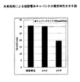
本発明者等は、このようにして形成された強誘電体キャパシタを、50μm×50μmのサイズにパターニングし、キャパシタ特性の測定を行った。図3は、かかるキャパシタ特性の測定結果を示す。
【0023】
図3を参照するに、「積層構造」で示した強誘電体キャパシタ試料および「x=1.4」で示した強誘電体キャパシタ試料では、キャパシタの分極を示す反転電荷量Qswの値が3Vの印加電圧においてで30μC/cm2を超えているのに対し、x=2.0のみの条件ではQSWの値が20μC/cm2程度しかないことがわかる。これは、低電圧動作が要求される状況では、「x=2.0」で示す強誘電体キャパシタ試料は使用することができないことを意味する。またこのことは、強誘電体キャパシタの上部電極として、IrOxの酸化の割合が小さい、酸素欠損を多量に含む膜を使うことにより、キャパシタ特性が向上することを意味する。このような現象が生じるメカニズムについては後で説明する。
【0024】
図4は、図3の実験におけるIrOx膜のスパッタリングの際の雰囲気と、得られたPZT膜の反転電荷量QSWとの関係を示す。ただし図4の実験は図3の試料「x=1.4」および「x=2.0」に対応しており、単層のIrOx膜を50°Cの温度で200nmの厚さに堆積している。
【0025】
図4を参照するに、スパッタリングの際のO2流量を約60SCCMに設定した場合(試料「x=1.4」)、Ar流量が60〜150SCCMの範囲では、PZT膜の反転電荷量QSWの値が25.0μC/cm2以上になるのに対し、前記O2流量を約100SCCMに設定すると(試料「x=2.0」)、前記反転電荷量QSWの値は15〜17μC/cm2程度まで減少することがわかる。
【0026】
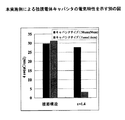
次に、前記強誘電体キャパシタ試料「積層構造」および「x=1.4」について、さらに前記強誘電体キャパシタ上にAlの3層配線構造を形成し、50μm×50μmおよび1.0μm×1.6μmのサイズにパターニングした後、このようにして得られた強誘電体キャパシタについて電気特性を測定した結果を図5に示す。
【0027】
図5を参照するに、キャパシタサイズが50μm×50μmの場合「積層構造」試料と「x=1.4」試料との間に実質的な電気特性の違いは見られない。一方、1.0μm×1.6μmのサイズにパターニングしたキャパシタでは、「積層構造」試料の反転電荷量QSWの値がキャパシタサイズが50μm×50μmサイズの場合と実質的に変わらないが、「x=1.4」の試料では、反転電荷量QSWの値が実質的に0μC/cm2に近い値になっているのがわかる。これは、キャパシタサイズが小さくなることにより、キャパシタ形成後に行われる多層配線構造の形成工程でのダメージによりPZT膜14が劣化し、反転電荷量QSWの値が大きく減少するものと考えられる。
【0028】
図3〜5の結果から、「x=1.4」の試料あるいは「x=2.0」の試料の条件で形成された強誘電体キャパシタは、微細化や多層配線構造との組み合わせが要求される実用的な半導体装置には使えないことがわかる。図5の結果はまた、多層配線構造の形成を含む後工程でのダメージに強い強誘電体キャパシタを実現するには、上部電極を、IrOx層15(x=1.4)上に、x>1.4で、可能ならば化学量論組成x=2に近いIrOx膜16を積層することにより形成するのが望ましいことを示している。
【0029】
このような現象が生じるメカニズムは、以下のようなものであると考えられる。
【0030】
金属状態のIrは水素触媒として作用することが周知である。すなわち、金属状態のIrと接触すると水素は活性化される。一方、前記IrOx膜15(x=1.4)中では、組成パラメータxの値が化学量論組成x=2.0よりも小さいため酸素欠損が生じており、酸化物成分と金属成分が混在している。そのため、前記上部電極の全体がIrOx膜15により形成されている場合、層間絶縁膜形成工程や配線パターン形成工程で生じる水素が活性化されてしまい、かかる活性化された水素によりキャパシタ特性が劣化してしまう。
【0031】
一方、化学量論組成に近いIrOx膜16(x=2)中には、酸素欠損が少なく金属Ir成分がほとんど含まれていないため水素が活性化されにくく、強誘電体キャパシタ上に多層配線構造を形成した後でも、キャパシタ特性が劣化せずに維持されると考えられる。
【0032】
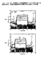
図6(A)、(B)は、このようにして形成された積層構造を有する強誘電体キャパシタの断面構造を示すSEM写真である。ただし図6(B)は図6(A)の一部を拡大して示している。また図7に、図6(B)の写真をスケッチした図を示す。
【0033】
図6(A),(B)および図7を参照するに、前記PZT膜14上の上部電極は、厚さが約100nmのIrOx層15(x=1.4)と、厚さが同じく約100nmのIrOx層16とより構成されているのが認められ、前記IrOx層15は粒径が100nm程度の粒状結晶の配列よりグラニュラー構造を有するのがわかる。これに対し、前記IrOx膜16は、粒径20〜50nm程度の柱状結晶より構成される柱状微構造を有するのがわかる。
【0034】
先にも説明したように、一般的にIrOxは、水素雰囲気中で金属状態のIrに還元しやすい性質を持っており、金属状態のIrに還元されてしまうと触媒作用により水素が活性化されてしまいキャパシタ特性が劣化する。これに対し、IrOx層16を構成する柱状結晶は他構造に比べてエネルギー的に安定な構造であると考えられ、柱状構造を有するIrOx層16は還元されにくく、このためキャパシタへの還元雰囲気によるダメージを抑制することができるものと考えられる。
【0035】
図8(A),(B)は、図6(B)の積層構造上部電極において、IrOx膜15とIrOx膜16の膜厚比を変化させた場合の断面SEM写真を示す。ただし図8(A)は図6(A),(B)の構造に対応し、IrOx膜15を100nmの厚さに形成した後で急速加熱処理を725°Cで20秒間行い、その後で前記IrOx膜15上にIrOx膜16を100nmの厚さに形成した場合を示すのに対し、図8(B)は前記IrOx膜15を約150nmの厚さに形成した後前記725°C,20秒間の急速加熱処理を行い、その後で前記IrOx膜16を50nmの厚さに形成した場合を示す。
【0036】
図8(A),(B)を参照するに、図8(A)の構造ではPZT膜14が柱状微構造を有し、大きな空孔などの欠陥は認められない。これに対し、図8(B)の構造では前記PZT膜14は柱状構造を有してはいるものの、大きな空孔が生じているのが観察される。このような大きな空孔を強誘電体膜中に含む強誘電体キャパシタは不良であり、FeRAMとして使用することはできない。
【0037】
図8(A),(B)の結果より、前記IrOx層15の膜厚は100nm以下であるのが望ましい。
【0038】
図6(A),(B)あるいは図8(A),(B)において、前記PZT膜14とその上のIrOx膜15との界面は実質的に平坦であり、結晶粒界に対応するような凹凸が見られないが、これは図1(C)の工程においてPZT膜をより低い第1の温度での急速熱処理により部分的に結晶化させ、さらに図2(E)の工程で前記IrOx膜15により前記PZT膜14を覆った後、図2(F)の工程でより高い第2の温度で急速熱処理を行い、前記PZT膜14を結晶化させた場合に特徴的に得られる構造である。
【0039】
図9(A)は、前記積層構造上部電極を有する強誘電体キャパシタ(先の「積層構造」試料)に関して行ったSIMS分析の結果を、また図9(B)は前記上部電極としてx=1.4のIrOx膜のみを使った強誘電体キャパシタ(先の「x=1.4」試料)についてのSIMS分析の結果を示す。
【0040】
図9(A)を参照するに、「積層構造」の試料では、下層のIrOx膜15中にはPZT膜14からのPbの拡散が生じているのが確認されるが、上層のIrOx膜16中におけるPbの濃度は検出限界以下であり、前記IrOx膜16中にはPbの拡散が生じていないと結論される。なお、図9(A)では上層IrOx膜16と下層IrOx膜15との界面にPbの濃集が観察されるが、これは前記膜15と16との界面における急激な膜質変化に伴う分析上のみかけだけの効果であり、実際にかかるPbの濃集が生じているわけではない。
【0041】
一方、図9(B)に示す「x=1.4」の試料では、Pbは上層のIrOx膜16の表面まで達しているのがわかる。また先に図3で説明した「x=2.0」の試料の場合、図9(A)のIrOx膜16中におけるPbの濃度が検出限界以下であることから、前記x=2.0の組成を有するIrOx膜よりなる上部電極中には、Pbは侵入していないものと考えられる。
【0042】
このように、先に示した図3の結果は、前記PZT膜14からIrOx膜15へのPbの実質的な拡散が生じているにもかかわらず強誘電体キャパシタの特性が、Pbの拡散が生じない場合よりも向上することを示しているが、そのメカニズムは次のように考えられる。
【0043】
先に述べたようにIrOx膜15(x=1.4)は酸素欠損を高濃度で含んでいる。そのため、かかるIrOx膜15では、酸素欠損により形成された空孔を伝わってPbが容易に拡散する。その結果、前記PZT膜14中に導入されている過剰なPbが前記IrOx膜15中に拡散し、その結果として前記PZT膜14と接するIrOx膜15の界面が平坦になるものと考えられる。前記IrOx膜15とPZT膜14との界面が平坦化された結果、前記強誘電体キャパシタに電圧を印加した場合、前記PZT膜14に印加される実効的な電圧が大きくなり、キャパシタ特性が向上するものと考えられる。
【0044】
次に、図2(F)の強誘電体キャパシタを有するFeRAMにおいて、多層配線構造を設ける場合に前記IrOx膜15および16に課せられる制約について検討する。
【0045】
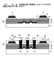
図10は、前記Si基板11上に図2(F)の強誘電体キャパシタを覆うように層間絶縁膜17を形成し、平坦化した後前記層間絶縁膜17中に前記IrOx膜16を露出するコンタクトホール17Aを形成し、さらに前記層間絶縁膜17上に前記コンタクトホール17Aにおいて前記IrOx膜16とコンタクトするようにAl等の配線パターン18を形成した状態を示す。
【0046】
多数の強誘電体キャパシタがSi基板11上に形成されたFeRAM集積回路装置においてこのように前記層間絶縁膜17中にコンタクトホール17Aを形成する場合、前記層間絶縁膜17の膜厚変化や個々の強誘電体キャパシタの高さのばらつきを考慮して、前記コンタクトホール17Aを形成するドライエッチング工程は、前記IrOx膜16の表面を露出するに必要な時間よりも多少長く継続される。その結果、前記IrOx膜16中には、図11に示すように、前記コンタクトホール17Aの底部に対応して凹部が形成され、かかる凹部において前記Al配線パターンが前記IrOx膜16とコンタクトさせられる。なお図10の写真では、前記Al配線パターン18が前記IrOx膜16とコンタクトする部分にTiNバリア層17Aが形成されているのが見える。
【0047】
このような多層配線構造とのコンタクト構造を形成する場合、前記IrOx膜16中の凹部の深さは一般に数十ナノメートルになる。図示の例では、前記凹部の深さは約50nmとなっている。従って、前記IrOx膜16の厚さが50nm以下であると、前記凹部において前記IrOx膜15が露出してしまい、その結果かかるコンタクトホールを介して水素などの還元性成分がIrOx膜15に侵入してしまい、PZT膜14の特性を劣化させる問題が生じる。このため、前記IrOx膜16の厚さは数十ナノメートル以上であることが必要であることがわかる。
【0048】
このように上層のIrOx膜16において多層配線構造とのコンタクトを行うことにより、前記IrOx膜16のプロセスダメージ耐性により、多層配線構造形成プロセスあるいはコンタクトホール形成プロセスの際の非酸化雰囲気の影響が強誘電体キャパシタ中の強誘電体膜に及ぶのを抑制することができる。
【0049】
なお、上記の説明は、下部電極13として前記Pt/Ti積層構造を使ったが、前記下部電極としてIrやRu、RuO2あるいはSrRuO3などの導電性酸化物もしくはそれらの積層構造でも構わない。
【0050】
さらに、前記下層上部電極15としてはIrOx膜以外にも、RuOx膜やSrRuOx膜などの非化学量論組成を有する導電性酸化物膜を使うことが可能で、一方前記上層上部電極16として、より化学量論組成に近い組成を有するIrOx膜以外にRuOx膜やSrRuOx膜などの導電性酸化物膜で、前記下層上部電極膜15より化学量論組成に近い組成を有する膜を使うことも可能である。
【0051】
また、本実施例において、前記PZT膜14の代わりに、PLZT膜、SBT(SrBi2(Ta,Nb)2O9)膜、あるいはBi層状化合物を使うことも可能である。
[第2実施例]
図12(A)〜図13(E)は、本発明の第2実施例によるFeRAMの製造工程を示す。
【0052】
図12(A)を参照するに、Si基板21上には素子分離膜22により活性領域が画成されており、前記活性領域中においては前記Si基板上にゲート絶縁膜23を介してゲート電極24A,24Bが、FeRAMのワード線の一部として形成される。各々のゲート電極24Aおよび24Bはシリサイド低抵抗層24Cを担持し、前記Si基板21中には、前記ゲート電極24Aの両側にLDD領域21Aおよび21Bが形成されている。また前記Si基板21中には前記ゲート電極24Bの両側にLDD拡散21Cおよび21Dが形成されている。
【0053】
前記ゲート電極24A,24Bはそれぞれ側壁面上に側壁絶縁膜24a,24bおよび24c,24dを有し、前記Si基板21中には、前記側壁絶縁膜24aの外縁に略対応して拡散領域21Eが形成されている。同様に、前記Si基板21中には、前記側壁絶縁膜24dの外縁に略対応して拡散領域21Gが形成されており、前記Si基板21中には前記側壁絶縁膜24bの外縁と前記側壁絶縁膜24cの外縁との間に拡散領域21Fが形成されている。
【0054】
前記ゲート電極24A,24Bは前記Si基板21上に前記活性領域および前記素子分離膜22を覆うように形成されたSiON膜25により覆われ、さらに前記SiON膜25上にはSiO2よりなる層間絶縁膜26がCVD法により、約1000nmの厚さに形成される。
【0055】
前記層間絶縁膜26は引き続いてCMP法により平坦化され、さらにN2雰囲気中、600°C、30分間の熱処理により、脱ガスを行う。
【0056】
次に図12(B)の工程において前記層間絶縁膜26上にTi膜およびPt膜をそれぞれ約20nmおよび約175nmの厚さに順次スパッタリングすることにより、Pt/Ti積層構造を有する下部電極膜27を形成する。先にも説明したが、前記下部電極27は前記Pt/Ti積層構造を有するものに限定されることはなく、Ir膜やRu膜、RuO2膜やSrRuO3膜を積層したものでもよい。
【0057】
図12(B)の工程では、引き続きPZTあるいはPLZTなどの強誘電体膜28をRFスパッタリングにより、約200nmの厚さに形成する。このようにして形成された強誘電体膜28は、図12(B)の工程でさらにAr/O2雰囲気中、約600°Cの温度で急速熱処理を施され、部分的に結晶化させられる。
【0058】
かかる強誘電体膜28の熱処理工程の後、図12(B)の工程ではさらに前記表1に示す条件下でIrOx膜の反応性スパッタリングを行い、下層上部電極となるIrOx膜29を前記強誘電体膜28上に形成する。このようにして形成されたIrOx膜29は、x≒1.4程度の非化学量論組成を有している。
【0059】
図12(B)の工程では、さらに前記IrOx膜29の形成工程の後、O2雰囲気中、725°Cにおいて急速熱処理が施され、前記強誘電体膜28が結晶化させられる。
【0060】
次に図12(C)の工程において前記IrOx膜29上に別のIrOx膜30を、先に表2で説明した条件下で堆積する。このようにして形成されたIrOx膜30は、化学量論組成IrO2、あるいは前記IrOx膜29よりも前記化学量論組成に近い組成を有する。
【0061】
次に図13(D)の工程において前記膜27〜30はパターニングされ、その結果、前記層間絶縁膜26上に強誘電体キャパシタC1,C2が形成される。
【0062】
さらに図13(E)の工程において前記層間絶縁膜26上に別の層間絶縁膜31が形成され、前記別の層間絶縁膜31中には前記拡散領域21E,21Fおよび21Gを露出するコンタクトホール31A〜31Cが形成され、前記コンタクトホール31A〜31Cは前記拡散領域21E〜21GとそれぞれコンタクトするW等の導電性プラグ31a〜31cにより充填される。
【0063】
また前記層間絶縁膜31中には前記キャパシタC1の上層IrOx電極層30を露出するコンタクトホール30Dと前記キャパシタC2の上層IrOx電極層30を露出するコンタクトホール30Eとが形成されており、前記層間絶縁膜31上には、前記コンタクトホール30Dにおいて前記キャパシタC1の前記上層IrOx電極層30とコンタクトし前記コンタクトホール31Aにおいて前記導電性プラグ31aとコンタクトするAl配線パターン32Aと、前記コンタクトホール31Bにおいて前記導電性プラグ31bとコンタクトするAl配線パターン32Bと、前記コンタクトホール31Cにおいて前記導電性プラグ31cとコンタクトし前記コンタクトホール30Eにおいて前記キャパシタC2のIrOx電極層とコンタクトするAl配線パターン32Cとが形成されている。
【0064】
前記IrOx電極層29上に、前記電極層29よりも化学量論組成に近いIrOx電極層30を形成することにより、前記コンタクトホール30Dあるいは30E形成時に使われる非酸化雰囲気あるいは前記Al配線パターン32A〜32Cの形成時に使われる非酸化雰囲気が前記IrOxないしIrO2電極層30により阻止され、前記キャパシタC1およびC2中において前記強誘電体膜28の電気特性の劣化が回避される。
【0065】
また前記強誘電体膜28に接する下層IrOx電極層29として、例えば組成パラメータxが1.4の非化学量論組成のIrOx膜を使うことにより、前記強誘電体膜28からPbが前記IrOx膜29に拡散し、前記強誘電体膜28とIrOx膜29との界面が平坦化する。その結果、前記強誘電体キャパシタC1,C2は優れた電気的特性を示す。先にも図9(A),(B)で説明したように、このように前記IrOx膜29中に前記強誘電体膜28から拡散したPbは、その上のIrOx膜30中には拡散しない。
【0066】
なお、以上の説明ではIrOxを上部電極層29,30として用いたが、本発明はIrOxに限定されるものではなく、前記上部電極層29,30としてRuOxやSrRuOx等の導電性酸化物を使うことも可能である。その際、前記上部電極層29,30として酸化の割合の異なる異種の酸化物を組み合わせて使うことも可能である。
【0067】
以下、異種の酸化物を上部電極層上層部30と上部電極層下層部29に使う場合について説明する。
【0068】
例えば上部電極層下層部29を先に述べた表1の条件で形成した場合、上部電極層上層部30としてSrRuOx膜を使うことが可能である。この場合、前記SrRuOx膜30の形成は、表面モフォロジーの劣化を回避するため、酸素雰囲気中での反応性スパッタリングではなくAr雰囲気中でのスパッタ法により行うのが好ましい。
【0069】
このようにして上部電極層上層部30を形成した後、O2雰囲気中、725°C,20秒間の急速加熱処理を行い、前記強誘電体膜28を結晶化させた後、さらに酸素雰囲気中650°Cで60分間アニール処理を行い、前記SrRuOx電極層30を酸化させる。SrRuOx膜は、いきなり炉アニールを行うと表面異常が生じてしまうため、本発明では最初に表面異常が生じない急速加熱処理を行い、それから前記急速加熱処理よりも低い温度で長時間、炉による熱処理を行うことにより、表面異常を発生させずに十分に酸化したSrRuOx膜を得ることができる。一方、このような長時間の熱処理を行っても、前記IrOx膜の酸化が進行することはない。Irの酸化には、1000°Cを超える高い温度が必要であり、前記IrOx電極層29における金属状態のIrの割合は、このような熱処理によっては変化しない。このようにして、先に示した実施例と同様に、上部電極の下層部よりも上層部の方が酸素の割合が高い構造を形成することができる。
【0070】
このような上部電極の上層部30と下層部29とで酸化の割合を変化させ、さらに図6(A)および(B)で示したような組織構造を得るには、上層部30の形成時と下層部29の形成時においてAr/O2の流量比を表1および表2あるいは図4に従って変化させればよいが、前記表1および表2に従ってスパッタパワーあるいは基板温度を変化させてもよい。一般にスパッタパワーが大きくなると、形成されるIrOx膜中での金属状態のIrの割合が増大する。また基板温度が高くなると、形成されるIrOx膜中での金属状態のIrの割合が減少する。
【0071】
また、本実施例において前記上部電極膜29および30の厚さ、および前記電極膜29および30の合計膜厚は、本実施例記載のものに限定されるものではない。
【0072】
さらに図14の変形例に示すように、前記下層IrOx電極層29を成膜後パターニングし、その上に前記上層IrOx電極層30を形成するようにしてもよい。ただし図14中、先に説明した部分には対応する参照符号を付し、説明を省略する。
【0073】
以上、本発明を好ましい実施例について説明したが、本発明はかかる特定の実施例に限定されるものではなく、特許請求の範囲に記載した要旨内において様々な変形・変更が可能である。
【0074】
(付記1) 基板と、
前記基板上に形成された強誘電体キャパシタとよりなる半導体装置において、前記強誘電体キャパシタは、下部電極と、前記下部電極上に形成された強誘電体膜と、前記強誘電体膜上に形成された上部電極とよりなり、
前記上部電極は、化学量論組成が組成パラメータx1を使って化学式AOx1で表され実際の組成が組成パラメータx2を使って化学式AOx2で表される酸化物よりなる第1の層と、前記第1の層上に形成され、化学量論組成が組成パラメータy1を使って化学式BOy1で表され実際の組成が組成パラメータy2を使って化学式BOy2で表される酸化物よりなる第2の層とよりなり、
前記組成パラメータx1,x2,y1およびy2の間には、関係
y2/y1>x2/x1
が成立することを特徴とする半導体装置。
【0075】
(付記2) 第1の層および第2の層の各々は、導電性酸化物よりなることを特徴とする付記1記載の半導体装置。
【0076】
(付記3) 前記第1の層は、前記第2の層を構成する金属元素と同じ金属元素により構成されることを特徴とする付記1または2記載の半導体装置。
【0077】
(付記4) 前記金属元素は、Ir,Ru,Pt,Pd,Os,SrおよびTaより選ばれることを特徴とする付記3記載の半導体装置。
【0078】
(付記5) 前記第1の層はIrOx2(x2<2)で表される組成を有し、前記第2の層はIrOy2(y2>x2)で表される組成を有することを特徴とする付記3記載の半導体装置。
【0079】
(付記6) 前記第1の層を構成する金属元素と前記第2の層を構成する金属元素とは異なっていることを特徴とする付記1または2記載の半導体装置。
【0080】
(付記7) 前記第1の層は化学量論組成がIrO2で実際の組成がIrOx2(x2<2)で表される組成を有し、前記第2の層は化学量論組成がSrRuO3で実際の組成がSrRuOy2で表される組成を有し、y2/3>x2/2であることを特徴とする付記6記載の半導体装置。
【0081】
(付記8) 強誘電体膜は、PZT膜、SBT膜、あるいはBi層状化合物よりなることを特徴とする付記1〜7のうち、いずれか一項記載の半導体装置。
【0082】
(付記9) 前記第1の層はグラニュラー状微構造を有し、前記第2の層は、結晶粒径が20〜50nmの柱状微構造を有することを特徴とする付記1〜8のうち、いずれか一項記載の半導体装置。
【0083】
(付記10) 前記第1の層は100nm以下の膜厚を有することを特徴とする付記1〜9のうち、いずれか一項記載の半導体装置。
【0084】
(付記11) 前記強誘電体膜と前記第1の膜との界面が平坦であることを特徴とする付記1〜10のうち、いずれか一項記載の半導体装置。
【0085】
(付記12) 前記第1の層はPbを含み、前記第2の層は実質的にPbを含まないことを特徴とする付記1〜11のうち、いずれか一項記載の半導体装置。
【0086】
(付記13) さらに前記基板上に、前記強誘電体キャパシタを覆うように多層配線構造が設けられ、前記第2の層が前記多層配線構造中の配線パターンと、コンタクトホールを介して接続されることを特徴とする付記1〜12のうち、いずれか一項記載の半導体装置。
【0087】
(付記14) 下部電極を形成する工程と、
前記下部電極上に強誘電体膜を堆積する工程と、
前記強誘電体膜上に第1の導電性酸化膜を堆積する工程と、
前記第1の導電性酸化膜上に第2の導電性酸化膜を堆積する工程とよりなり、前記第1の導電性酸化膜の堆積工程を、前記第2の導電性酸化膜の堆積工程におけるよりもより酸化性の弱い条件下において実行することを特徴とする半導体装置の製造方法。
【0088】
(付記15) 強誘電体膜を堆積する工程の後、前記第1の導電性酸化膜を堆積する工程の前に、前記強誘電体膜を不活性ガスと酸化性ガスの混合雰囲気中、第1の温度で熱処理する工程を含み、
さらに前記第1の導電性酸化膜を堆積する工程の後、前記強誘電体膜を、酸化雰囲気中、前記第1の温度よりも高い第2の温度で熱処理し、前記強誘電体膜を結晶化する工程を含むことを特徴とする付記14記載の半導体装置の製造方法。
【0089】
(付記16) 前記第1の導電性酸化膜を堆積する工程と前記第2の導電性酸化膜を堆積する工程とは、反応性スパッタリングにより実行されることを特徴とする付記14または15記載の半導体装置の製造方法
(付記17) 前記第2の導電性酸化膜を堆積する工程は、前記第1の導電性酸化膜を堆積する工程におけるスパッタパワーよりも低いスパッタパワーで実行されることを特徴とする付記16記載の半導体装置の製造方法。
【0090】
(付記18) 前記第2の導電性酸化膜を堆積する工程は、前記第1の導電性酸化膜を堆積する工程におけるスパッタ雰囲気よりもより酸化性のスパッタ雰囲気中において実行されることを特徴とする付記16または17記載の半導体装置の製造方法。
【0091】
(付記19) 前記第1の導電性酸化膜を堆積する工程は、Ir,Ru,Pt,Pd,Os,SrRuOx,InTaOx,およびそれらの合金より選択されるターゲットを使って実行され、前記第2の導電性酸化膜を堆積する工程は、Ir,Ru,Pt,Pd,Os,SrRuOx,InTaOx,およびそれらの合金より選択されるターゲットを使って実行されることを特徴とする付記14〜18のうち、いずれか一項記載の半導体装置の製造方法。
【0092】
【発明の効果】
本発明によれば、動作電圧の低減を可能にする強誘電体キャパシタの電気特性の向上と同時に、半導体集積回路装置に要求される微細化や配線多層化に対応する際の強誘電体キャパシタへのダメージが抑制され、優れたFeRAMおよびその集積回路装置を形成することができる。
【図面の簡単な説明】
【図1】(A)〜(C)は、本発明の第1実施例による強誘電体キャパシタの製造工程を示す図(その1)である。
【図2】(D)〜(E)は、本発明の第1実施例による強誘電体キャパシタの製造工程を示す図(その2)である。
【図3】本実施例による強誘電体キャパシタの電気特性を示す図である。
【図4】IrOx上部電極形成時のスパッタ雰囲気と強誘電体キャパシタの電気特性の関係を示す図である。
【図5】本実施例による強誘電体キャパシタの電気特性を示す別の図である。
【図6】(A),(B)は、本実施例による強誘電体キャパシタの断面構造のSEM像を示す図である。
【図7】図6(B)の断面構造を概略的にスケッチした図である。
【図8】(A).(B)は、本発明による強誘電体キャパシタの断面構造のSEM像を、異なった処理条件について比較して示す図である。
【図9】(A),(B)は、本発明による強誘電体キャパシタ中における元素分布を、比較対照試料中の元素分布と比較して示す図である。
【図10】本実施例の強誘電体キャパシタに多層配線構造を設けた場合の構造を示す図である。
【図11】図10の構成においてコンタクトホール近傍を拡大したSEM像を示す図である。
【図12】(A)〜(C)は、本発明の第2実施例によるFeRAMの製造工程を示す図(その1)である。
【図13】(D),(E)は、本発明の第2実施例によるFeRAMの製造工程を示す図(その2)である。
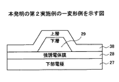
【図14】本発明の第2実施例の一変形例を示す図である。
【符号の説明】
11 Si基板
12 SiO2膜
13 下部電極
13A Ti膜
13B Pt膜
14 PZT膜
15 IrOx下層上部電極膜
16 IrOx上層上部電極膜
17 層間絶縁膜
17A コンタクトホール
18 Al配線パターン
21 Si基板
21A,21B,21C,21D LDD領域
21E,21F 拡散領域
22 素子分離膜
23 ゲート絶縁膜
24A,24B ゲート電極
24C シリサイド層
24a,24b,24c,24d 側壁絶縁膜
25 SiON膜
26 層間絶縁膜
27 下部電極
28 上部電極
29 IrOx上部電極下層部
30 IrOx上部電極上層部
31 層間絶縁膜
31A,31B,31C,31D,31E コンタクトホール
31a,31b,31c 導電性プラグ
32A,32B,32C Al配線パターン[0001]
BACKGROUND OF THE INVENTION
The present invention generally relates to semiconductor devices, and more particularly to a semiconductor device having a ferroelectric film and a method of manufacturing the same.
[0002]
A ferroelectric memory device (FeRAM) is a nonvolatile semiconductor memory device that can retain stored information even when the power is turned off. In FeRAM, information is stored using the hysteresis characteristic of a ferroelectric substance.
[0003]
A typical FeRAM has a ferroelectric capacitor in which a ferroelectric film is sandwiched between a pair of electrodes, and information is stored by inducing polarization in the ferroelectric capacitor according to an applied voltage between the electrodes. To do. Information written in the form of polarization in the ferroelectric film in this way is retained even when the applied voltage is removed.
In such a ferroelectric capacitor, if the polarity of the applied voltage is reversed, the polarity of the spontaneous polarization is also reversed. Therefore, the written information can be read by detecting the spontaneous polarization. FeRAM operates at a lower voltage than a flash memory, and can write information at high speed with low power.
[0004]
[Prior art]
By the way, in such FeRAM, it is necessary to repeatedly perform heat treatment in an oxygen atmosphere in the manufacturing process of FeRAM in order to recover the characteristic deterioration of the ferroelectric film accompanying the processing in the non-oxidizing atmosphere. Ferroelectric films that make up ferroelectric capacitors easily cause oxygen vacancies due to processing in a non-oxidizing atmosphere, and as a result, the characteristics of the ferroelectric film, such as the amount of inversion charge and leakage current, deteriorate. End up. For this reason, conventionally, a metal that is not easily oxidized even in an oxygen atmosphere such as Pt, or a conductive oxide such as IrOx or RuOx is used as the upper electrode.
[0005]
[Problems to be solved by the invention]
Incidentally, in recent years, strict requirements for miniaturization have been imposed on FeRAM, and accordingly, miniaturization of ferroelectric capacitors and the use of a multilayer wiring structure are required. Furthermore, low voltage operation is required in connection with application to a portable information processing apparatus.
[0006]
In order for FeRAM to be able to operate at a low voltage, a ferroelectric film constituting a ferroelectric capacitor has a large inversion charge QSWHowever, when a multilayer wiring structure is used, the characteristics of the already formed ferroelectric capacitor deteriorate due to the reducing atmosphere treatment or non-oxidizing atmosphere treatment used in the process of forming the multilayer wiring structure. Cause problems.
[0007]
More specifically, when the upper electrode is formed of a Pt film or an Ir film, hydrogen in a reducing atmosphere used when forming the interlayer insulating film in the multilayer wiring structure enters the Pt film or the Ir film. Thus, there is a problem that the ferroelectric film in the ferroelectric capacitor is reduced by the activated hydrogen due to the catalytic action of these metals, and the activated hydrogen is reduced. When the ferroelectric film is reduced, the operating characteristics of the ferroelectric capacitor are greatly degraded. Such a problem of deterioration of the characteristics of the ferroelectric film is particularly noticeable when the ferroelectric capacitor is miniaturized and the capacitor insulating film in the ferroelectric capacitor is composed of a miniaturized ferroelectric film pattern. .
[0008]
Accordingly, it is a general object of the present invention to provide a new and useful semiconductor device that solves the above-described problems and a method for manufacturing the same.
[0009]
A more specific problem of the present invention is that miniaturization of a ferroelectric capacitor can be achieved while suppressing deterioration of electrical characteristics of the ferroelectric film, and a multilayer wiring structure can be formed on the ferroelectric capacitor. And a semiconductor device manufactured by the manufacturing method.
[0010]
[Means for Solving the Problems]
The present invention provides a semiconductor device comprising a substrate and a ferroelectric capacitor formed on the substrate, wherein the ferroelectric capacitor includes a lower electrode and a strong electrode formed on the lower electrode. A dielectric film and an upper electrode formed on the ferroelectric film, the stoichiometric composition of the upper electrode being a composition parameter x1Using the chemical formula AOx1Where the actual composition is the composition parameter x2Using the chemical formula AOx2And a stoichiometric composition formed on the first layer, the composition parameter y1Use the chemical formula BOy1The actual composition is expressed by the composition parameter y2Use the chemical formula BOy2A second layer made of an oxide represented byFurthermore, the second layer is configured to have a higher oxidation rate than the first layer,The composition parameter x1, X2, Y1And y2Between the relationship y2/ Y1> X2/ X1This is solved by a semiconductor device characterized in that
[0011]
The present invention also has the above-described problems, a step of forming a lower electrode, a step of depositing a ferroelectric film on the lower electrode, and a step of depositing a first conductive oxide film on the ferroelectric film. And a step of depositing a second conductive oxide film on the first conductive oxide film, and the step of depositing the first conductive oxide film includes the step of depositing the second conductive oxide film. More than in the processO against Ar flow rate 2 Small flow rateRun under conditionsIn the second conductive oxide film, the oxidation rate is higher than that in the first conductive oxide film.This is solved by a method for manufacturing a semiconductor device.
[Action]
According to the present invention, by using the first conductive oxide film having a non-stoichiometric composition as the lower upper electrode layer in contact with the ferroelectric film constituting the capacitor insulating film of the ferroelectric capacitor, Pb diffused from the dielectric film into the lower upper electrode layer, and accordingly, the interface between the ferroelectric film and the lower upper electrode layer was flattened, and a voltage was applied to the ferroelectric capacitor. In this case, the effective voltage value applied to the ferroelectric film becomes larger and the capacitor characteristics are improved. On the other hand, when a conductive film having such a non-stoichiometric composition is exposed to an atmosphere containing hydrogen, the metal component in the film activates hydrogen, and the activated hydrogen is a characteristic of the ferroelectric film. Deteriorate. Therefore, in the present invention, the second conductivity having a stoichiometric composition or a composition closer to the stoichiometric composition is formed on the lower upper electrode layer.Oxide filmAn upper upper electrode layer is formed to prevent a reducing atmosphere from entering the lower upper electrode layer.
[0012]
DETAILED DESCRIPTION OF THE INVENTION
[First embodiment]
According to the present invention, in a FeRAM having a multilayer wiring structure, miniaturization of a ferroelectric capacitor can be realized while suppressing deterioration of the ferroelectric film. Hereinafter, a method for manufacturing a ferroelectric capacitor according to the first embodiment of the present invention will be described.
[0013]
The inventors of the present invention used a PZT film formed on a lower electrode having a Pt / Ti structure as a capacitor insulating film and a ferroelectric having an IrOx film as an upper electrode in the experimental research that is the basis of the present invention. The following knowledge was obtained through experiments to fabricate capacitors.
[0014]
Hereinafter, experiments conducted by the inventors of the present invention will be described with reference to FIGS. 1A to 2F corresponding to the manufacturing process of the ferroelectric capacitor according to the first embodiment of the present invention. .
[0015]
Referring to FIG. 1A, 1000 nm thick SiO 2 formed on the Si substrate 11.2On the
[0016]
Next, in the step of FIG. 1B, a
[0017]
2D, the
[0018]
[Table 1]
[0019]
[Table 2]
[0020]
[Table 3]
[0021]
Further, in an experiment conducted by the present inventors, a ferroelectric capacitor sample in which a single-layer IrOx film was formed as a top electrode on the
[0022]
The inventors of the present invention patterned the ferroelectric capacitor thus formed to a size of 50 μm × 50 μm, and measured the capacitor characteristics. FIG. 3 shows the measurement results of such capacitor characteristics.
[0023]
Referring to FIG. 3, in the ferroelectric capacitor sample indicated by “laminated structure” and the ferroelectric capacitor sample indicated by “x = 1.4”, the inversion charge amount Q indicating the polarization of the capacitor is obtained.swOf 30 μC / cm at an applied voltage of 3V2In the condition of x = 2.0 onlySWValue of 20 μC / cm2You can see that there is only a degree. This means that the ferroelectric capacitor sample indicated by “x = 2.0” cannot be used in a situation where low voltage operation is required. This also means that the capacitor characteristics are improved by using a film containing a small amount of IrOx oxidation and containing a large amount of oxygen vacancies as the upper electrode of the ferroelectric capacitor. The mechanism by which such a phenomenon occurs will be described later.
[0024]
4 shows the atmosphere during sputtering of the IrOx film in the experiment of FIG. 3, and the inversion charge amount Q of the obtained PZT film.SWShows the relationship. However, the experiment of FIG. 4 corresponds to the samples “x = 1.4” and “x = 2.0” of FIG. 3, and a single-layer IrOx film is deposited at a temperature of 50 ° C. to a thickness of 200 nm. ing.
[0025]
Referring to FIG. 4, O during sputtering2When the flow rate is set to about 60 SCCM (sample “x = 1.4”), when the Ar flow rate is in the range of 60 to 150 SCCM, the inversion charge amount Q of the PZT filmSWValue of 25.0 μC / cm2On the other hand, the O2When the flow rate is set to about 100 SCCM (sample “x = 2.0”), the inversion charge amount QSWThe value of 15-17 μC / cm2It can be seen that it decreases to the extent.
[0026]
Next, for the ferroelectric capacitor samples “laminated structure” and “x = 1.4”, an Al three-layer wiring structure is further formed on the ferroelectric capacitor, and 50 μm × 50 μm and 1.0 μm × 1 FIG. 5 shows the result of measuring the electrical characteristics of the ferroelectric capacitor thus obtained after patterning to a size of .6 μm.
[0027]
Referring to FIG. 5, when the capacitor size is 50 μm × 50 μm, there is no substantial difference in electrical characteristics between the “laminated structure” sample and the “x = 1.4” sample. On the other hand, in a capacitor patterned to a size of 1.0 μm × 1.6 μm, the inverted charge amount Q of the “stacked structure” sampleSWIs substantially the same as the case where the capacitor size is 50 μm × 50 μm, but in the sample of “x = 1.4”, the inversion charge amount Q isSWIs substantially 0 μC / cm2You can see that it is close to. This is because the
[0028]
From the results shown in FIGS. 3 to 5, the ferroelectric capacitor formed under the conditions of “x = 1.4” or “x = 2.0” requires the miniaturization and combination with the multilayer wiring structure. It can be seen that it cannot be used for practical semiconductor devices. The result of FIG. 5 also shows that the upper electrode is placed on the IrOx layer 15 (x = 1.4) and x> 1 in order to realize a ferroelectric capacitor that is resistant to damage in the subsequent process including the formation of the multilayer wiring structure. 1.4 indicates that it is desirable to stack the
[0029]
The mechanism by which such a phenomenon occurs is considered as follows.
[0030]
It is well known that Ir in the metal state acts as a hydrogen catalyst. That is, hydrogen is activated upon contact with Ir in the metal state. On the other hand, in the IrOx film 15 (x = 1.4), since the value of the composition parameter x is smaller than the stoichiometric composition x = 2.0, oxygen vacancies occur, and the oxide component and the metal component are mixed. doing. Therefore, when the entire upper electrode is formed of the
[0031]
On the other hand, the IrOx film 16 (x = 2) close to the stoichiometric composition has few oxygen vacancies and hardly contains a metal Ir component, so that hydrogen is hardly activated, and a multilayer wiring structure is formed on the ferroelectric capacitor. Even after forming the capacitor, it is considered that the capacitor characteristics are maintained without deterioration.
[0032]
6A and 6B are SEM photographs showing the cross-sectional structure of the ferroelectric capacitor having the multilayer structure formed as described above. However, FIG. 6B is an enlarged view of a part of FIG. FIG. 7 shows a sketch of the photograph of FIG.
[0033]
Referring to FIGS. 6A, 6B and 7, the upper electrode on the
[0034]
As described above, IrOx generally has a property of being easily reduced to Ir in a metal state in a hydrogen atmosphere, and when reduced to Ir in the metal state, hydrogen is activated by catalytic action. As a result, the capacitor characteristics deteriorate. On the other hand, the columnar crystals constituting the
[0035]
8A and 8B are cross-sectional SEM photographs in the case where the thickness ratio of the
[0036]
8A and 8B, in the structure of FIG. 8A, the
[0037]
From the results shown in FIGS. 8A and 8B, the film thickness of the
[0038]
In FIGS. 6A and 6B or FIGS. 8A and 8B, the interface between the
[0039]
FIG. 9A shows the results of SIMS analysis performed on a ferroelectric capacitor having the multilayer structure upper electrode (the previous “laminate structure” sample), and FIG. 9B shows x = 1 as the upper electrode. 4 shows the results of SIMS analysis of a ferroelectric capacitor using only an IrOx film of .4 (the previous “x = 1.4” sample).
[0040]
Referring to FIG. 9A, in the “laminated structure” sample, it is confirmed that Pb diffusion from the
[0041]
On the other hand, in the sample of “x = 1.4” shown in FIG. 9B, it can be seen that Pb reaches the surface of the
[0042]
As described above, the result of FIG. 3 shown above shows that the characteristics of the ferroelectric capacitor are substantially the same as the Pb diffusion although the substantial diffusion of Pb from the
[0043]
As described above, the IrOx film 15 (x = 1.4) contains oxygen vacancies at a high concentration. Therefore, in such an
[0044]
Next, the restrictions imposed on the
[0045]
In FIG. 10, an
[0046]
In the FeRAM integrated circuit device in which a large number of ferroelectric capacitors are formed on the
[0047]
When a contact structure with such a multilayer wiring structure is formed, the depth of the recess in the
[0048]
By making contact with the multilayer wiring structure in the
[0049]
In the above description, the Pt / Ti laminated structure is used as the
[0050]
In addition to the IrOx film, it is possible to use a conductive oxide film having a non-stoichiometric composition such as a RuOx film or a SrRuOx film as the lower layer
[0051]
In this embodiment, a PLZT film, SBT (SrBi) is used instead of the PZT film 14.2(Ta, Nb)2O9It is also possible to use membranes or Bi layered compounds.
[Second Embodiment]
FIGS. 12A to 13E show the manufacturing process of FeRAM according to the second embodiment of the present invention.
[0052]
Referring to FIG. 12A, an active region is defined on an
[0053]
The
[0054]
The
[0055]
The
[0056]
Next, in the step of FIG. 12B, a Ti film and a Pt film are sequentially sputtered on the
[0057]
In the step of FIG. 12B, a
[0058]
After the heat treatment process of the
[0059]
In the step of FIG. 12B, after the formation step of the
[0060]
Next, in the step of FIG. 12C, another
[0061]
Next, in the step of FIG. 13D, the
[0062]
Further, in the step of FIG. 13E, another
[0063]
In the
[0064]
By forming an
[0065]
Further, as the lower
[0066]
In the above description, IrOx is used as the upper electrode layers 29 and 30, but the present invention is not limited to IrOx, and conductive oxides such as RuOx and SrRuOx are used as the upper electrode layers 29 and 30. It is also possible. At this time, different types of oxides having different oxidation rates may be used in combination as the upper electrode layers 29 and 30.
[0067]
Hereinafter, a case where different kinds of oxides are used for the upper electrode layer
[0068]
For example, when the upper electrode layer
[0069]
After forming the upper electrode layer
[0070]
In order to change the rate of oxidation between the
[0071]
In the present embodiment, the thicknesses of the
[0072]
Further, as shown in the modification of FIG. 14, the lower
[0073]
Although the present invention has been described with reference to the preferred embodiments, the present invention is not limited to such specific embodiments, and various modifications and changes can be made within the scope described in the claims.
[0074]
(Appendix 1) a substrate,
In the semiconductor device including the ferroelectric capacitor formed on the substrate, the ferroelectric capacitor includes a lower electrode, a ferroelectric film formed on the lower electrode, and the ferroelectric film. It consists of the upper electrode formed,
The upper electrode has a stoichiometric composition parameter x1Using the chemical formula AOx1Where the actual composition is the composition parameter x2Using the chemical formula AOx2And a stoichiometric composition formed on the first layer, the composition parameter y1Use the chemical formula BOy1The actual composition is expressed by the composition parameter y2Use the chemical formula BOy2A second layer made of an oxide represented by
The composition parameter x1, X2, Y1And y2The relationship between
y2/ Y1> X2/ X1
A semiconductor device, wherein
[0075]
(Supplementary note 2) The semiconductor device according to supplementary note 1, wherein each of the first layer and the second layer is made of a conductive oxide.
[0076]
(Additional remark 3) The said 1st layer is comprised with the same metal element as the metallic element which comprises said 2nd layer, The semiconductor device of Additional remark 1 or 2 characterized by the above-mentioned.
[0077]
(Supplementary note 4) The semiconductor device according to supplementary note 3, wherein the metal element is selected from Ir, Ru, Pt, Pd, Os, Sr and Ta.
[0078]
(Supplementary Note 5) The first layer is made of IrOx.2(X2<2) and the second layer is IrOy2(Y2> X2The semiconductor device according to appendix 3, wherein the semiconductor device has a composition represented by:
[0079]
(Supplementary note 6) The semiconductor device according to Supplementary note 1 or 2, wherein the metal element constituting the first layer and the metal element constituting the second layer are different.
[0080]
(Supplementary Note 7) The first layer has a stoichiometric composition of IrO.2And the actual composition is IrOx2(X2<2) and the second layer has a stoichiometric composition of SrRuO.ThreeAnd the actual composition is SrRuOy2And having a composition represented by y2/ 3> x2The semiconductor device according to appendix 6, wherein the semiconductor device is / 2.
[0081]
(Supplementary note 8) The semiconductor device according to any one of supplementary notes 1 to 7, wherein the ferroelectric film is made of a PZT film, an SBT film, or a Bi layered compound.
[0082]
(Supplementary note 9) Of the supplementary notes 1 to 8, wherein the first layer has a granular microstructure, and the second layer has a columnar microstructure with a crystal grain size of 20 to 50 nm. The semiconductor device according to any one of claims.
[0083]
(Supplementary note 10) The semiconductor device according to any one of supplementary notes 1 to 9, wherein the first layer has a thickness of 100 nm or less.
[0084]
(Supplementary Note 11) The semiconductor device according to any one of Supplementary notes 1 to 10, wherein an interface between the ferroelectric film and the first film is flat.
[0085]
(Supplementary note 12) The semiconductor device according to any one of Supplementary notes 1 to 11, wherein the first layer includes Pb, and the second layer substantially does not include Pb.
[0086]
(Additional remark 13) Furthermore, a multilayer wiring structure is provided on the substrate so as to cover the ferroelectric capacitor, and the second layer is connected to a wiring pattern in the multilayer wiring structure via a contact hole. 14. The semiconductor device according to any one of appendices 1 to 12, characterized in that:
[0087]
(Additional remark 14) The process of forming a lower electrode,
Depositing a ferroelectric film on the lower electrode;
Depositing a first conductive oxide film on the ferroelectric film;
A step of depositing a second conductive oxide film on the first conductive oxide film, and the step of depositing the first conductive oxide film in the step of depositing the second conductive oxide film. A method for manufacturing a semiconductor device, which is performed under a condition that is less oxidizable than the semiconductor device.
[0088]
(Supplementary Note 15) After the step of depositing the ferroelectric film, the step of depositing the ferroelectric film in a mixed atmosphere of an inert gas and an oxidizing gas before the step of depositing the first conductive oxide film. Including a step of heat treatment at a temperature of 1,
Further, after the step of depositing the first conductive oxide film, the ferroelectric film is heat-treated in an oxidizing atmosphere at a second temperature higher than the first temperature, and the ferroelectric film is crystallized. 15. The method of manufacturing a semiconductor device according to
[0089]
(Supplementary Note 16) The
(Supplementary note 17) The
[0090]
(Supplementary Note 18) The step of depositing the second conductive oxide film is performed in a sputtering atmosphere that is more oxidizing than the sputtering atmosphere in the step of depositing the first conductive oxide film. 18. A method for manufacturing a semiconductor device according to
[0091]
(Supplementary Note 19) The step of depositing the first conductive oxide film is performed using a target selected from Ir, Ru, Pt, Pd, Os, SrRuOx, InTaOx, and alloys thereof, and The step of depositing the conductive oxide film is performed using a target selected from Ir, Ru, Pt, Pd, Os, SrRuOx, InTaOx, and alloys thereof. A method for manufacturing a semiconductor device according to any one of the above.
[0092]
【The invention's effect】
According to the present invention, the ferroelectric capacitor that can reduce the operating voltage is improved, and at the same time, the ferroelectric capacitor can be used for miniaturization and multilayer wiring required for a semiconductor integrated circuit device. Therefore, an excellent FeRAM and its integrated circuit device can be formed.
[Brief description of the drawings]
FIGS. 1A to 1C are views (No. 1) showing a manufacturing process of a ferroelectric capacitor according to a first embodiment of the invention; FIGS.
FIGS. 2D to 2E are views (No. 2) showing the manufacturing process of the ferroelectric capacitor according to the first embodiment of the invention; FIGS.
FIG. 3 is a diagram showing the electrical characteristics of the ferroelectric capacitor according to this example.
FIG. 4 is a diagram showing the relationship between the sputtering atmosphere when forming an IrOx upper electrode and the electrical characteristics of a ferroelectric capacitor.
FIG. 5 is another diagram showing electrical characteristics of the ferroelectric capacitor according to this example.
FIGS. 6A and 6B are SEM images of a cross-sectional structure of a ferroelectric capacitor according to this example.
7 is a schematic sketch of the cross-sectional structure of FIG. 6 (B).
FIG. 8 (A). (B) is a diagram showing an SEM image of a cross-sectional structure of a ferroelectric capacitor according to the present invention in comparison with different processing conditions.
FIGS. 9A and 9B are diagrams showing the element distribution in the ferroelectric capacitor according to the present invention in comparison with the element distribution in the comparative sample. FIGS.
FIG. 10 is a diagram showing a structure when a multilayer wiring structure is provided in the ferroelectric capacitor of this example.
11 is a view showing an SEM image in which the vicinity of a contact hole is enlarged in the configuration of FIG.
FIGS. 12A to 12C are views (No. 1) showing the manufacturing process of FeRAM according to the second embodiment of the present invention; FIGS.
FIGS. 13D and 13E are views (No. 2) showing the manufacturing process of FeRAM according to the second embodiment of the present invention; FIGS.
FIG. 14 is a view showing a modification of the second embodiment of the present invention.
[Explanation of symbols]
11 Si substrate
12 SiO2film
13 Lower electrode
13A Ti film
13B Pt film
14 PZT film
15 IrOx lower layer upper electrode film
16 IrOx upper layer upper electrode film
17 Interlayer insulation film
17A contact hole
18 Al wiring pattern
21 Si substrate
21A, 21B, 21C, 21D LDD region
21E, 21F Diffusion region
22 Device isolation membrane
23 Gate insulation film
24A, 24B Gate electrode
24C silicide layer
24a, 24b, 24c, 24d Side wall insulating film
25 SiON film
26 Interlayer insulation film
27 Lower electrode
28 Upper electrode
29 IrOx upper electrode lower layer
30 IrOx upper electrode upper layer
31 Interlayer insulation film
31A, 31B, 31C, 31D, 31E Contact hole
31a, 31b, 31c conductive plug
32A, 32B, 32C Al wiring pattern
Claims (9)
前記基板上に形成された強誘電体キャパシタとよりなる半導体装置において、
前記強誘電体キャパシタは、下部電極と、前記下部電極上に形成された強誘電体膜と、前記強誘電体膜上に形成された上部電極とよりなり、
前記上部電極は、化学量論組成が組成パラメータx1を使って化学式AOx1で表され実際の組成が組成パラメータx2を使って化学式AOx2で表される酸化物よりなる第1の層と、前記第1の層上に形成され、化学量論組成が組成パラメータy1を使って化学式BOy1で表され実際の組成が組成パラメータy2を使って化学式BOy2で表される酸化物よりなる第2の層とよりなり、さらに、前記第2の層は前記第1の層より酸化の割合が高く構成され、
前記組成パラメータx1,x2,y1およびy2の間には、関係
y2/y1>x2/x1
が成立することを特徴とする半導体装置。A substrate,
In a semiconductor device comprising a ferroelectric capacitor formed on the substrate,
The ferroelectric capacitor includes a lower electrode, a ferroelectric film formed on the lower electrode, and an upper electrode formed on the ferroelectric film,
The upper electrode includes a first layer made of an oxide having a stoichiometric composition represented by the chemical formula AOx 1 using the composition parameter x 1 and an actual composition represented by the chemical formula AOx 2 using the composition parameter x 2. The oxide is formed on the first layer, the stoichiometric composition is represented by the chemical formula BOy 1 using the composition parameter y 1 , and the actual composition is represented by the chemical formula BOy 2 using the composition parameter y 2. The second layer is configured to have a higher oxidation rate than the first layer,
Between the composition parameters x 1 , x 2 , y 1 and y 2 , the relationship y 2 / y 1 > x 2 / x 1
A semiconductor device, wherein
前記下部電極上に強誘電体膜を堆積する工程と、
前記強誘電体膜上に第1の導電性酸化膜を堆積する工程と、
前記第1の導電性酸化膜上に第2の導電性酸化膜を堆積する工程とよりなり、
前記第1の導電性酸化膜の堆積工程を、前記第2の導電性酸化膜の堆積工程におけるよりもよりAr流量に対するO 2 流量の割合が小さい条件下において実行し、前記第2の導電性酸化膜において、前記第1の導電性酸化膜よりも酸化の割合を高くすることを特徴とする半導体装置の製造方法。Forming a lower electrode;
Depositing a ferroelectric film on the lower electrode;
Depositing a first conductive oxide film on the ferroelectric film;
Depositing a second conductive oxide film on the first conductive oxide film,
The step of depositing said first conductive oxide film, run under conditions ratio of O 2 flow rate is less for a more Ar flow rate than in the step of depositing said second conductive oxide film, said second conductive A method of manufacturing a semiconductor device, characterized in that an oxidation rate of the oxide film is higher than that of the first conductive oxide film .
さらに前記第1の導電性酸化膜を堆積する工程の後、前記強誘電体膜を、酸化雰囲気中、前記第1の温度よりも高い第2の温度で熱処理し、前記強誘電体膜を結晶化する工程を含むことを特徴とする請求項7記載の半導体装置の製造方法。After the step of depositing the ferroelectric film and before the step of depositing the first conductive oxide film, the ferroelectric film is placed in a mixed atmosphere of an inert gas and an oxidizing gas at a first temperature. Including a step of heat treatment,
Further, after the step of depositing the first conductive oxide film, the ferroelectric film is heat-treated at a second temperature higher than the first temperature in an oxidizing atmosphere, and the ferroelectric film is crystallized. The method of manufacturing a semiconductor device according to claim 7, further comprising a step of forming the semiconductor device.
Priority Applications (6)
| Application Number | Priority Date | Filing Date | Title |
|---|---|---|---|
| JP2001128373A JP3661850B2 (en) | 2001-04-25 | 2001-04-25 | Semiconductor device and manufacturing method thereof |
| EP01122797A EP1253627B1 (en) | 2001-04-25 | 2001-09-21 | Semiconductordevice having a ferroelectric capacitor and fabrication process thereof |
| US09/962,452 US6624458B2 (en) | 2001-04-25 | 2001-09-26 | Semiconductor device having a ferroelectric capacitor and fabrication process thereof |
| TW090123950A TW560047B (en) | 2001-04-25 | 2001-09-27 | Semiconductor device having a ferroelectric capacitor and fabrication process thereof |
| KR1020010066778A KR100857699B1 (en) | 2001-04-25 | 2001-10-29 | Semiconductor Device Having a Ferroelectric Capacitor and Fabrication Process Thereof |
| US10/465,546 US6740533B2 (en) | 2001-04-25 | 2003-06-20 | Semiconductor device having a ferroelectric capacitor and fabrication process thereof |
Applications Claiming Priority (1)
| Application Number | Priority Date | Filing Date | Title |
|---|---|---|---|
| JP2001128373A JP3661850B2 (en) | 2001-04-25 | 2001-04-25 | Semiconductor device and manufacturing method thereof |
Publications (2)
| Publication Number | Publication Date |
|---|---|
| JP2002324894A JP2002324894A (en) | 2002-11-08 |
| JP3661850B2 true JP3661850B2 (en) | 2005-06-22 |
Family
ID=18977076
Family Applications (1)
| Application Number | Title | Priority Date | Filing Date |
|---|---|---|---|
| JP2001128373A Expired - Fee Related JP3661850B2 (en) | 2001-04-25 | 2001-04-25 | Semiconductor device and manufacturing method thereof |
Country Status (5)
| Country | Link |
|---|---|
| US (2) | US6624458B2 (en) |
| EP (1) | EP1253627B1 (en) |
| JP (1) | JP3661850B2 (en) |
| KR (1) | KR100857699B1 (en) |
| TW (1) | TW560047B (en) |
Cited By (3)
| Publication number | Priority date | Publication date | Assignee | Title |
|---|---|---|---|---|
| US7605007B2 (en) * | 2007-03-09 | 2009-10-20 | Fujitsu Microelectronics Limited | Semiconductor device and method of manufacturing the same |
| US8390045B2 (en) | 2007-03-20 | 2013-03-05 | Fujitsu Semiconductor Limited | Semiconductor device and method of manufacturing same |
| US8405188B2 (en) | 2007-02-28 | 2013-03-26 | Fujitsu Semiconductor Limited | Semiconductor device and method of manufacturing the semiconductor device |
Families Citing this family (32)
| Publication number | Priority date | Publication date | Assignee | Title |
|---|---|---|---|---|
| US7473949B2 (en) | 2002-12-10 | 2009-01-06 | Fujitsu Limited | Ferroelectric capacitor and method of manufacturing the same |
| CN100369255C (en) * | 2002-12-10 | 2008-02-13 | 富士通株式会社 | Ferroelectric capacitor and method for manufacturing the same |
| US20040163233A1 (en) * | 2003-02-26 | 2004-08-26 | Stefan Gernhardt | Methods of forming electrical connections within ferroelectric devices |
| JP2004296929A (en) * | 2003-03-27 | 2004-10-21 | Seiko Epson Corp | Manufacturing method of ferroelectric capacitor, ferroelectric capacitor, storage element, electronic element, memory device, and electronic equipment |
| JP2004296923A (en) * | 2003-03-27 | 2004-10-21 | Seiko Epson Corp | Manufacturing method of ferroelectric capacitor, ferroelectric capacitor, storage element, electronic element, memory device, and electronic equipment |
| JP2005183842A (en) * | 2003-12-22 | 2005-07-07 | Fujitsu Ltd | Manufacturing method of semiconductor device |
| JP2005183841A (en) * | 2003-12-22 | 2005-07-07 | Fujitsu Ltd | Manufacturing method of semiconductor device |
| WO2005074032A1 (en) * | 2004-01-28 | 2005-08-11 | Fujitsu Limited | Semiconductor device and its manufacturing method |
| JP3910209B2 (en) * | 2004-03-05 | 2007-04-25 | 松下電器産業株式会社 | Piezoelectric element, inkjet head, angular velocity sensor, manufacturing method thereof, and inkjet recording apparatus |
| JP4528943B2 (en) * | 2004-04-27 | 2010-08-25 | 独立行政法人産業技術総合研究所 | Capacitance temperature sensor and temperature measuring device |
| US20060011129A1 (en) * | 2004-07-14 | 2006-01-19 | Atomic Energy Council - Institute Of Nuclear Energy Research | Method for fabricating a compound semiconductor epitaxial wafer |
| JP4913994B2 (en) * | 2004-08-09 | 2012-04-11 | セイコーエプソン株式会社 | Ferroelectric capacitor, ferroelectric memory, ferroelectric capacitor manufacturing method, and ferroelectric memory manufacturing method |
| JP2006073648A (en) * | 2004-08-31 | 2006-03-16 | Fujitsu Ltd | Semiconductor device and manufacturing method thereof |
| JP4589092B2 (en) * | 2004-12-03 | 2010-12-01 | 富士通セミコンダクター株式会社 | Manufacturing method of semiconductor device |
| JP2006302975A (en) * | 2005-04-15 | 2006-11-02 | Toshiba Corp | Semiconductor device and manufacturing method thereof |
| JP4887827B2 (en) * | 2006-02-20 | 2012-02-29 | 富士通セミコンダクター株式会社 | Method for forming ferroelectric capacitor and method for manufacturing semiconductor device |
| JP5140935B2 (en) * | 2006-03-28 | 2013-02-13 | 富士通セミコンダクター株式会社 | Magnetron sputtering film forming apparatus and semiconductor device manufacturing method |
| JP2007266429A (en) * | 2006-03-29 | 2007-10-11 | Fujitsu Ltd | Semiconductor device and manufacturing method thereof |
| JP4690234B2 (en) * | 2006-03-31 | 2011-06-01 | 富士通セミコンダクター株式会社 | Semiconductor device and manufacturing method thereof |
| JP4882548B2 (en) * | 2006-06-30 | 2012-02-22 | 富士通セミコンダクター株式会社 | Semiconductor device and manufacturing method thereof |
| JP4827653B2 (en) | 2006-08-10 | 2011-11-30 | 富士通セミコンダクター株式会社 | Semiconductor device and manufacturing method thereof |
| JP4983172B2 (en) * | 2006-09-12 | 2012-07-25 | 富士通セミコンダクター株式会社 | Semiconductor device and manufacturing method thereof |
| JP5104850B2 (en) * | 2007-02-28 | 2012-12-19 | 富士通セミコンダクター株式会社 | Manufacturing method of semiconductor device |
| CN101627470B (en) | 2007-03-14 | 2011-12-28 | 富士通半导体股份有限公司 | Semiconductor device and process for producing the same |
| JP5380784B2 (en) | 2007-04-12 | 2014-01-08 | ソニー株式会社 | Autofocus device, imaging device, and autofocus method |
| JP2008270596A (en) * | 2007-04-23 | 2008-11-06 | Toshiba Corp | Ferroelectric memory and manufacturing method of ferroelectric memory |
| US7812425B2 (en) * | 2007-10-05 | 2010-10-12 | Kabushiki Kaisha Toshiba | Semiconductor device with lower capacitor electrode that includes islands of conductive oxide films arranged on a noble metal film |
| US8124528B2 (en) * | 2008-04-10 | 2012-02-28 | Micron Technology, Inc. | Method for forming a ruthenium film |
| JP2010278074A (en) * | 2009-05-26 | 2010-12-09 | Fujitsu Semiconductor Ltd | Electronic device and manufacturing method thereof |
| JP5593935B2 (en) | 2010-08-04 | 2014-09-24 | 富士通セミコンダクター株式会社 | Ferroelectric capacitor manufacturing method and ferroelectric capacitor |
| JP5360161B2 (en) * | 2011-08-17 | 2013-12-04 | 富士通セミコンダクター株式会社 | Semiconductor device and manufacturing method thereof |
| JP5561300B2 (en) * | 2012-03-26 | 2014-07-30 | 富士通セミコンダクター株式会社 | Manufacturing method of semiconductor device |
Family Cites Families (13)
| Publication number | Priority date | Publication date | Assignee | Title |
|---|---|---|---|---|
| US5554564A (en) * | 1994-08-01 | 1996-09-10 | Texas Instruments Incorporated | Pre-oxidizing high-dielectric-constant material electrodes |
| JP3171110B2 (en) | 1996-06-19 | 2001-05-28 | ソニー株式会社 | Method of manufacturing ferroelectric capacitor structure |
| US5790366A (en) * | 1996-12-06 | 1998-08-04 | Sharp Kabushiki Kaisha | High temperature electrode-barriers for ferroelectric and other capacitor structures |
| JP3183243B2 (en) * | 1998-02-25 | 2001-07-09 | 日本電気株式会社 | Thin film capacitor and method of manufacturing the same |
| US6541375B1 (en) * | 1998-06-30 | 2003-04-01 | Matsushita Electric Industrial Co., Ltd. | DC sputtering process for making smooth electrodes and thin film ferroelectric capacitors having improved memory retention |
| JP2000091539A (en) * | 1998-07-16 | 2000-03-31 | Fujitsu Ltd | Semiconductor device and manufacturing method thereof |
| KR100268424B1 (en) * | 1998-08-07 | 2000-10-16 | 윤종용 | A method of fabricating interconnect of semiconductor device |
| JP3159255B2 (en) * | 1998-09-16 | 2001-04-23 | 日本電気株式会社 | Sputter growth method for electrodes used in ferroelectric capacitors |
| JP3468706B2 (en) * | 1998-09-17 | 2003-11-17 | 富士通株式会社 | Semiconductor device and manufacturing method thereof |
| JP2000157471A (en) | 1998-11-27 | 2000-06-13 | Toto Ltd | Dish washer |
| KR100329774B1 (en) * | 1998-12-22 | 2002-05-09 | 박종섭 | Method for forming capacitor of ferroelectric random access memory device |
| US6388285B1 (en) * | 1999-06-04 | 2002-05-14 | International Business Machines Corporation | Feram cell with internal oxygen source and method of oxygen release |
| US20020117700A1 (en) * | 2001-02-28 | 2002-08-29 | Glex Fox | Amorphous iridium oxide barrier layer and electrodes in ferroelectric capacitors |
-
2001
- 2001-04-25 JP JP2001128373A patent/JP3661850B2/en not_active Expired - Fee Related
- 2001-09-21 EP EP01122797A patent/EP1253627B1/en not_active Expired - Lifetime
- 2001-09-26 US US09/962,452 patent/US6624458B2/en not_active Expired - Lifetime
- 2001-09-27 TW TW090123950A patent/TW560047B/en not_active IP Right Cessation
- 2001-10-29 KR KR1020010066778A patent/KR100857699B1/en not_active Expired - Fee Related
-
2003
- 2003-06-20 US US10/465,546 patent/US6740533B2/en not_active Expired - Lifetime
Cited By (6)
| Publication number | Priority date | Publication date | Assignee | Title |
|---|---|---|---|---|
| US8405188B2 (en) | 2007-02-28 | 2013-03-26 | Fujitsu Semiconductor Limited | Semiconductor device and method of manufacturing the semiconductor device |
| US8664011B2 (en) | 2007-02-28 | 2014-03-04 | Fujitsu Limited | Semiconductor device and method of manufacturing the semiconductor device |
| US7605007B2 (en) * | 2007-03-09 | 2009-10-20 | Fujitsu Microelectronics Limited | Semiconductor device and method of manufacturing the same |
| US8390045B2 (en) | 2007-03-20 | 2013-03-05 | Fujitsu Semiconductor Limited | Semiconductor device and method of manufacturing same |
| US8609440B2 (en) | 2007-03-20 | 2013-12-17 | Fujitsu Semiconductor Limited | Semiconductor device and method of manufacturing same |
| US8629487B2 (en) | 2007-03-20 | 2014-01-14 | Fujitsu Semiconductor Limited | Semiconductor device and method of manufacturing same |
Also Published As
| Publication number | Publication date |
|---|---|
| US6624458B2 (en) | 2003-09-23 |
| TW560047B (en) | 2003-11-01 |
| US20030213986A1 (en) | 2003-11-20 |
| US6740533B2 (en) | 2004-05-25 |
| EP1253627A3 (en) | 2003-10-22 |
| US20020185668A1 (en) | 2002-12-12 |
| JP2002324894A (en) | 2002-11-08 |
| KR20020083104A (en) | 2002-11-01 |
| KR100857699B1 (en) | 2008-09-08 |
| EP1253627A2 (en) | 2002-10-30 |
| EP1253627B1 (en) | 2012-06-13 |
Similar Documents
| Publication | Publication Date | Title |
|---|---|---|
| JP3661850B2 (en) | Semiconductor device and manufacturing method thereof | |
| US6590252B2 (en) | Semiconductor device with oxygen diffusion barrier layer termed from composite nitride | |
| JP2005150688A (en) | Semiconductor device and manufacturing method thereof | |
| JP2004296929A (en) | Manufacturing method of ferroelectric capacitor, ferroelectric capacitor, storage element, electronic element, memory device, and electronic equipment | |
| CN101203957B (en) | Manufacturing method of semiconductor device | |
| JP4421814B2 (en) | Capacitor element manufacturing method | |
| KR100668881B1 (en) | Capacitor and manufacturing method thereof | |
| JP4392336B2 (en) | Method for manufacturing ferroelectric capacitor | |
| JP2002203948A (en) | Semiconductor device | |
| JP2004193176A (en) | Semiconductor device and method of manufacturing the same | |
| WO2005081317A1 (en) | Process for fabricating semiconductor device | |
| JP2006059968A (en) | Semiconductor device and manufacturing method thereof, ferroelectric capacitor structure | |
| JP2003243628A (en) | Ferroelectric thin film, ferroelectric capacitor, and method of manufacturing ferroelectric memory element | |
| KR100943011B1 (en) | Semiconductor device and manufacturing method thereof | |
| JPH07273220A (en) | Capacitor formation method | |
| JP4267589B2 (en) | Wiring and manufacturing method thereof | |
| JP2007184440A (en) | Ferroelectric capacitor and manufacturing method thereof | |
| JP2007035947A (en) | Semiconductor device and manufacturing method thereof | |
| JP2001210796A (en) | Dielectric element | |
| JP2000357782A (en) | Semiconductor storage device and method of manufacturing the same | |
| WO2008004297A1 (en) | Semiconductor device comprising capacitor and method for manufacturing same | |
| JP2004296923A (en) | Manufacturing method of ferroelectric capacitor, ferroelectric capacitor, storage element, electronic element, memory device, and electronic equipment | |
| JP2007158366A (en) | Dielectric capacitor | |
| JP2004304015A (en) | Dielectric capacitor and method of manufacturing the same |
Legal Events
| Date | Code | Title | Description |
|---|---|---|---|
| A977 | Report on retrieval |
Free format text: JAPANESE INTERMEDIATE CODE: A971007 Effective date: 20041201 |
|
| A131 | Notification of reasons for refusal |
Free format text: JAPANESE INTERMEDIATE CODE: A131 Effective date: 20041221 |
|
| A521 | Request for written amendment filed |
Free format text: JAPANESE INTERMEDIATE CODE: A523 Effective date: 20050221 |
|
| TRDD | Decision of grant or rejection written | ||
| A01 | Written decision to grant a patent or to grant a registration (utility model) |
Free format text: JAPANESE INTERMEDIATE CODE: A01 Effective date: 20050315 |
|
| A61 | First payment of annual fees (during grant procedure) |
Free format text: JAPANESE INTERMEDIATE CODE: A61 Effective date: 20050316 |
|
| R150 | Certificate of patent or registration of utility model |
Free format text: JAPANESE INTERMEDIATE CODE: R150 |
|
| FPAY | Renewal fee payment (event date is renewal date of database) |
Free format text: PAYMENT UNTIL: 20080401 Year of fee payment: 3 |
|
| FPAY | Renewal fee payment (event date is renewal date of database) |
Free format text: PAYMENT UNTIL: 20090401 Year of fee payment: 4 |
|
| S111 | Request for change of ownership or part of ownership |
Free format text: JAPANESE INTERMEDIATE CODE: R313111 |
|
| FPAY | Renewal fee payment (event date is renewal date of database) |
Free format text: PAYMENT UNTIL: 20090401 Year of fee payment: 4 |
|
| R350 | Written notification of registration of transfer |
Free format text: JAPANESE INTERMEDIATE CODE: R350 |
|
| FPAY | Renewal fee payment (event date is renewal date of database) |
Free format text: PAYMENT UNTIL: 20090401 Year of fee payment: 4 |
|
| FPAY | Renewal fee payment (event date is renewal date of database) |
Free format text: PAYMENT UNTIL: 20100401 Year of fee payment: 5 |
|
| FPAY | Renewal fee payment (event date is renewal date of database) |
Free format text: PAYMENT UNTIL: 20110401 Year of fee payment: 6 |
|
| FPAY | Renewal fee payment (event date is renewal date of database) |
Free format text: PAYMENT UNTIL: 20110401 Year of fee payment: 6 |
|
| S531 | Written request for registration of change of domicile |
Free format text: JAPANESE INTERMEDIATE CODE: R313531 |
|
| S533 | Written request for registration of change of name |
Free format text: JAPANESE INTERMEDIATE CODE: R313533 |
|
| FPAY | Renewal fee payment (event date is renewal date of database) |
Free format text: PAYMENT UNTIL: 20110401 Year of fee payment: 6 |
|
| R350 | Written notification of registration of transfer |
Free format text: JAPANESE INTERMEDIATE CODE: R350 |
|
| FPAY | Renewal fee payment (event date is renewal date of database) |
Free format text: PAYMENT UNTIL: 20120401 Year of fee payment: 7 |
|
| FPAY | Renewal fee payment (event date is renewal date of database) |
Free format text: PAYMENT UNTIL: 20130401 Year of fee payment: 8 |
|
| FPAY | Renewal fee payment (event date is renewal date of database) |
Free format text: PAYMENT UNTIL: 20130401 Year of fee payment: 8 |
|
| FPAY | Renewal fee payment (event date is renewal date of database) |
Free format text: PAYMENT UNTIL: 20140401 Year of fee payment: 9 |
|
| S531 | Written request for registration of change of domicile |
Free format text: JAPANESE INTERMEDIATE CODE: R313531 |
|
| R350 | Written notification of registration of transfer |
Free format text: JAPANESE INTERMEDIATE CODE: R350 |
|
| LAPS | Cancellation because of no payment of annual fees |