JP3660650B2 - Manufacturing method of semiconductor device - Google Patents
Manufacturing method of semiconductor device Download PDFInfo
- Publication number
- JP3660650B2 JP3660650B2 JP2002172628A JP2002172628A JP3660650B2 JP 3660650 B2 JP3660650 B2 JP 3660650B2 JP 2002172628 A JP2002172628 A JP 2002172628A JP 2002172628 A JP2002172628 A JP 2002172628A JP 3660650 B2 JP3660650 B2 JP 3660650B2
- Authority
- JP
- Japan
- Prior art keywords
- dram
- memory
- region
- area
- wafer
- Prior art date
- Legal status (The legal status is an assumption and is not a legal conclusion. Google has not performed a legal analysis and makes no representation as to the accuracy of the status listed.)
- Expired - Lifetime
Links
- 238000004519 manufacturing process Methods 0.000 title claims description 60
- 239000004065 semiconductor Substances 0.000 title claims description 12
- 238000000034 method Methods 0.000 claims description 92
- 230000008569 process Effects 0.000 claims description 83
- 235000012431 wafers Nutrition 0.000 claims description 66
- 239000003990 capacitor Substances 0.000 claims description 36
- 230000015572 biosynthetic process Effects 0.000 claims description 32
- 238000003860 storage Methods 0.000 claims description 16
- 230000006870 function Effects 0.000 claims description 15
- 230000002093 peripheral effect Effects 0.000 claims description 10
- 238000005520 cutting process Methods 0.000 claims description 4
- 239000010410 layer Substances 0.000 description 20
- 238000002955 isolation Methods 0.000 description 16
- 239000011521 glass Substances 0.000 description 10
- 229910052751 metal Inorganic materials 0.000 description 10
- 239000002184 metal Substances 0.000 description 10
- 229920002120 photoresistant polymer Polymers 0.000 description 10
- 229910052785 arsenic Inorganic materials 0.000 description 9
- RQNWIZPPADIBDY-UHFFFAOYSA-N arsenic atom Chemical compound [As] RQNWIZPPADIBDY-UHFFFAOYSA-N 0.000 description 9
- 239000000758 substrate Substances 0.000 description 9
- 239000011229 interlayer Substances 0.000 description 8
- 229910021420 polycrystalline silicon Inorganic materials 0.000 description 8
- 239000000047 product Substances 0.000 description 8
- 238000013461 design Methods 0.000 description 7
- 230000000694 effects Effects 0.000 description 6
- 238000005530 etching Methods 0.000 description 6
- XUIMIQQOPSSXEZ-UHFFFAOYSA-N Silicon Chemical compound [Si] XUIMIQQOPSSXEZ-UHFFFAOYSA-N 0.000 description 5
- 238000001020 plasma etching Methods 0.000 description 5
- 229910021332 silicide Inorganic materials 0.000 description 5
- FVBUAEGBCNSCDD-UHFFFAOYSA-N silicide(4-) Chemical compound [Si-4] FVBUAEGBCNSCDD-UHFFFAOYSA-N 0.000 description 5
- 229910052710 silicon Inorganic materials 0.000 description 5
- 239000010703 silicon Substances 0.000 description 5
- 229910052581 Si3N4 Inorganic materials 0.000 description 4
- 239000000470 constituent Substances 0.000 description 4
- 238000010276 construction Methods 0.000 description 4
- 238000010586 diagram Methods 0.000 description 4
- 238000009792 diffusion process Methods 0.000 description 4
- 239000012535 impurity Substances 0.000 description 4
- 230000010354 integration Effects 0.000 description 4
- 238000004904 shortening Methods 0.000 description 4
- HQVNEWCFYHHQES-UHFFFAOYSA-N silicon nitride Chemical compound N12[Si]34N5[Si]62N3[Si]51N64 HQVNEWCFYHHQES-UHFFFAOYSA-N 0.000 description 4
- 238000007796 conventional method Methods 0.000 description 3
- 239000000463 material Substances 0.000 description 3
- WQJQOUPTWCFRMM-UHFFFAOYSA-N tungsten disilicide Chemical compound [Si]#[W]#[Si] WQJQOUPTWCFRMM-UHFFFAOYSA-N 0.000 description 3
- 229910021342 tungsten silicide Inorganic materials 0.000 description 3
- 238000003491 array Methods 0.000 description 2
- 230000008859 change Effects 0.000 description 2
- 230000006866 deterioration Effects 0.000 description 2
- 238000011156 evaluation Methods 0.000 description 2
- 239000003870 refractory metal Substances 0.000 description 2
- 238000000926 separation method Methods 0.000 description 2
- 229910004298 SiO 2 Inorganic materials 0.000 description 1
- VYPSYNLAJGMNEJ-UHFFFAOYSA-N Silicium dioxide Chemical compound O=[Si]=O VYPSYNLAJGMNEJ-UHFFFAOYSA-N 0.000 description 1
- RTAQQCXQSZGOHL-UHFFFAOYSA-N Titanium Chemical compound [Ti] RTAQQCXQSZGOHL-UHFFFAOYSA-N 0.000 description 1
- 229910052782 aluminium Inorganic materials 0.000 description 1
- XAGFODPZIPBFFR-UHFFFAOYSA-N aluminium Chemical compound [Al] XAGFODPZIPBFFR-UHFFFAOYSA-N 0.000 description 1
- 238000000137 annealing Methods 0.000 description 1
- 238000010923 batch production Methods 0.000 description 1
- 230000015556 catabolic process Effects 0.000 description 1
- 239000010941 cobalt Substances 0.000 description 1
- 229910017052 cobalt Inorganic materials 0.000 description 1
- GUTLYIVDDKVIGB-UHFFFAOYSA-N cobalt atom Chemical compound [Co] GUTLYIVDDKVIGB-UHFFFAOYSA-N 0.000 description 1
- 230000005684 electric field Effects 0.000 description 1
- 239000012467 final product Substances 0.000 description 1
- 238000010438 heat treatment Methods 0.000 description 1
- 238000005468 ion implantation Methods 0.000 description 1
- 230000014759 maintenance of location Effects 0.000 description 1
- 238000012986 modification Methods 0.000 description 1
- 230000004048 modification Effects 0.000 description 1
- 238000000206 photolithography Methods 0.000 description 1
- 238000012545 processing Methods 0.000 description 1
- 230000009467 reduction Effects 0.000 description 1
- 229910052814 silicon oxide Inorganic materials 0.000 description 1
- 239000010936 titanium Substances 0.000 description 1
- 229910052719 titanium Inorganic materials 0.000 description 1
- WFKWXMTUELFFGS-UHFFFAOYSA-N tungsten Chemical compound [W] WFKWXMTUELFFGS-UHFFFAOYSA-N 0.000 description 1
- 229910052721 tungsten Inorganic materials 0.000 description 1
- 239000010937 tungsten Substances 0.000 description 1
Images


Classifications
-
- H—ELECTRICITY
- H10—SEMICONDUCTOR DEVICES; ELECTRIC SOLID-STATE DEVICES NOT OTHERWISE PROVIDED FOR
- H10B—ELECTRONIC MEMORY DEVICES
- H10B12/00—Dynamic random access memory [DRAM] devices
- H10B12/30—DRAM devices comprising one-transistor - one-capacitor [1T-1C] memory cells
- H10B12/37—DRAM devices comprising one-transistor - one-capacitor [1T-1C] memory cells the capacitor being at least partially in a trench in the substrate
-
- H—ELECTRICITY
- H10—SEMICONDUCTOR DEVICES; ELECTRIC SOLID-STATE DEVICES NOT OTHERWISE PROVIDED FOR
- H10B—ELECTRONIC MEMORY DEVICES
- H10B12/00—Dynamic random access memory [DRAM] devices
- H10B12/01—Manufacture or treatment
- H10B12/09—Manufacture or treatment with simultaneous manufacture of the peripheral circuit region and memory cells
-
- H—ELECTRICITY
- H10—SEMICONDUCTOR DEVICES; ELECTRIC SOLID-STATE DEVICES NOT OTHERWISE PROVIDED FOR
- H10B—ELECTRONIC MEMORY DEVICES
- H10B12/00—Dynamic random access memory [DRAM] devices
- H10B12/50—Peripheral circuit region structures
-
- H—ELECTRICITY
- H10—SEMICONDUCTOR DEVICES; ELECTRIC SOLID-STATE DEVICES NOT OTHERWISE PROVIDED FOR
- H10B—ELECTRONIC MEMORY DEVICES
- H10B12/00—Dynamic random access memory [DRAM] devices
- H10B12/30—DRAM devices comprising one-transistor - one-capacitor [1T-1C] memory cells
- H10B12/48—Data lines or contacts therefor
- H10B12/482—Bit lines
Landscapes
- Engineering & Computer Science (AREA)
- Manufacturing & Machinery (AREA)
- Semiconductor Memories (AREA)
- Design And Manufacture Of Integrated Circuits (AREA)
- Semiconductor Integrated Circuits (AREA)
Description
【0001】
【発明の属する技術分野】
本発明は、メモリ領域およびメモリとは異なる機能を有する機能領域を含む半導体装置の製造方法に関し、特にメモリセルにトレンチキャパシタを使用したDRAM混載LSIの製造方法に使用されるものである。
【0002】
【従来の技術】
LSIは、DRAMやロジックLSIといったように、機能毎に異なったチップとして以前より製造されている。しかし、近年、LSIの高性能化への要請から、異なった機能を有するLSIをワンチップ化した、システムLSIあるいは混載LSIと称されるLSIとして製造されるようになってきている。
【0003】
この種のLSIは、従来の一品種で大量の需要の見込まれた汎用DRAMやロジックLSIとは異なり、少量多品種生産の製品であるとともに、製造の短期化が必要とされる製品である。
【0004】
ところが、DRAMとロジックLSIとのシステムLSI(DRAM混載LSI)においては、その製造工程を考えると、少量生産で品種毎にマスクが異なるためにマスク費用にコストがかかる。そのため、汎用DRAMやロジックLSI等のLSIに比べて、製造コストが高くなるという問題がある。
【0005】
さらに、品種毎に仕様に合わせたマスクを作製するために、マスクの作製に時間がかかり、製造期間の短期化が困難になるという問題がある。
【0006】
さらにまた、DRAMのメモリセルを構成するキャパシタとしてトレンチキャパシタを使用した場合、トレンチキャパシタの合計面積(占有面積)が品種毎に異なるために、エッチングの条件出しが品種毎に必要になる。
【0007】
すなわち、メモリセルを構成するトレンチキャパシタの深さおよびアスペクトが同じでも、メモリセル内のトレンチキャパシタの合計面積が異なると、トレンチのエッチング条件も変わってしまう。そのため、エッチングの条件出しが必要となり、製造期間の短期化がさらに困難になるという問題がある。
【0008】
【発明が解決しようとする課題】
上述の如く、DRAM混載LSIは少量多品種生産であることから、汎用DRAMやロジックLSI等のLSIに比べて、製造コストが高くなったり、製造期間の短期化が困難であるという問題がある。特に、DRAMのメモリセルにトレンチキャパシタを使用した場合、エッチングの条件出しが品種毎に必要になるため、製造期間の短期化がさらに困難になるという問題がある。
【0009】
本発明は、上記事情を考慮してなされたもので、その目的とするところは、製造期間の短縮化および製造コストの削減化を図れる、メモリ領域およびメモリとは異なる機能を有する機能領域を含む半導体装置の製造方法を提供することにある。
【0010】
【課題を解決するための手段】
本願において開示される発明のうち、代表的なものの概要を簡単に説明すれば下記の通りである。
【0012】
本発明に係る半導体装置の製造方法は、メモリ形成プロセスの所定の工程までが済んだ複数の同一構成のメモリ領域を有するウェハを用意する工程と、前記ウェハ内の前記複数の同一構成のメモリ領域の中から、作製しようとするメモリが必要とする記憶容量に対応した数が選択されたメモリ領域を含む前記ウェハ内の1つの領域について、前記メモリ形成プロセスの前記所定の工程よりも後の工程を行うとともに、前記1つの領域内に、メモリとは異なる機能を有する機能領域を形成する工程と、前記1つの領域を前記ウェハから切り出す工程とを有することを特徴とする。
【0013】
また、本発明に係る他の半導体装置の製造方法は、メモリ形成プロセスの所定の工程までが済んだ複数のメモリ領域を有する複数のウェハを用意する工程であって、同一ウェハ内の複数のメモリ領域は同一構成を有し、かつ前記メモリ領域の記憶容量はウェハ毎に異なる工程と、前記複数のウェハの中から1つのウェハを選択する工程と、前記選択したウェハ内の前記複数の同一構成のメモリ領域の中から、作製しようとするメモリが必要とする記憶容量に対応した数が選択されたメモリ領域を含む前記ウェハ内の1つの領域について、前記メモリ形成プロセスの前記所定の工程よりも後の工程を行うとともに、前記1つの領域内に、メモリとは異なる機能を有する機能領域を形成する工程と、前記1つの領域を前記ウェハから切り出す工程とを有することを特徴とする。
【0015】
すなわち、メモリ形成プロセスの所定の工程までが済んだ複数の同一構成のメモリ領域を有するウェハを用意しておき、上記複数のメモリ領域のうち実際に必要となる記憶容量に対応した数のメモリ領域を使用することにより、メモリを最初から形成する従来の方法に比べて、実質的な製造期間(受注から製造が終了するまでの期間)を短縮することができる。
【0016】
また、ウェハに形成するシステムLSIの品種に関係なく、上記複数の同一構成のメモリ領域は同じマスクを用いて形成されるものなので、マスク費用のコストを削減化でき、その結果として製造コストの削減化を図れるようになる。
【0017】
本発明の上記ならびにその他の目的と新規な特徴は、本明細書の記載および添付図面によって明らかになるであろう。
【0018】
【発明の実施の形態】
以下、図面を参照しながら本発明の実施形態を説明する。
【0019】
(第1の実施形態)
本実施形態では、本発明をDRAM混載LSIに適用した場合について説明する。
【0020】
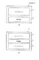
まず、図1に示すように、チップ領域1中に占めるDRAM領域21 〜24 の面積比率がそれぞれ5%、20%、50%、75%のウェハ31 〜34 を予め準備しておく(ステップS1)。
【0021】
記憶容量はDRAM領域21 〜24 の順で多くなる。DRAM領域21 〜24 の面積比率を同じにして、DRAM領域21 〜24 毎に記憶容量を変えることも可能である。
【0022】
DRAM領域21 〜24 内には、それぞれ、図2に示すように、メモリセルアレイ4とそれを駆動するための周辺回路5とを含むDRAMコア6が形成されている。DRAMコア6にはいくつかのタイプがあるが、図2には代表的な二つのタイプが示されている。図2(a)には一対のメモリセルアレイ4と周辺回路5とで構成されたタイプ、図2(b)には周辺回路5の上下にそれぞれメモリセルアレイ4が配置されたタイプが示されている。
【0023】
メモリセルアレイ4は、1つのトレンチキャパシタと1つのMOSトランジスタとで構成された所謂1Tr/1Cのメモリセルが集積化されたものである。ここでは、メモリセルアレイ4は、図3のトレンチキャパシタ形成に係わる工程までが済んだものとする。
【0024】
図3のトレンチキャパシタ形成に係わる工程について説明すると、まず、図3(a)に示すように、(100)面方位を有するn型のシリコン基板11上にトレンチ形成用のマスクパターン12を形成し、これをマスクに用いてシリコン基板11の表面をRIE(Reactive Ion Etching)プロセスによりエッチングし、トレンチ13を形成する。
【0025】
マスクパターン12は、シリコン酸化膜とその上に形成されたシリコン窒化膜とからなる積層絶縁膜をフォトリソグラフィおよびエッチングを用いて加工することにより形成する。
【0026】
次に、図3(b)に示すように、トレンチ13の側面および底面を被覆するように砒素ドープガラス膜14を全面に形成した後、トレンチ13内をその途中の深さまでフォトレジスト15で埋め込む。
【0027】
フォトレジスト15は、以下のようにして形成する。すなわち、ポジ型のフォトレジストを全面に塗布し、次にトレンチ13の中央部よりも上の部分のフォトレジストだけを露光し、最後にフォトレジストを現像して、その上部だけを除去することで、フォトレジスト15が得られる。
【0028】
次に、図3(c)に示すように、フォトレジスト15をマスクにして砒素ドープガラス膜14をエッチングして、フォトレジスト15よりも上の部分のトレンチ13の側面を露出させ、その後図示しないCVD酸化膜を全面に形成してから、熱処理により砒素ドープガラス膜14中の砒素(n型不純物)を基板中に拡散させ、n型の拡散層(プレート電極)16を形成する。CVD酸化膜は、砒素ドープガラス膜14中の砒素の気相への拡散を防止し、所望濃度の拡散層16を容易に形成するためのものである。
【0029】
この後、マスクパターン12、砒素ドープガラス膜14、フォトレジスト15およびCVD酸化膜を除去する。
【0030】
次に、図3(d)に示すように、キャパシタ絶縁膜17をトレンチ13の側面および底面を被覆するように全面に形成し、その後トレンチ13の内部を充填するように、第1ストレージノード電極となる砒素等の不純物を含む第1多結晶シリコン膜18を全面に堆積する。
【0031】
次に、図3(e)に示すように、第1多結晶シリコン膜18をRIEプロセスによってエッチバックして第1ストレージノード電極18を形成し、その後第1ストレージノード電極18をマスクにしてキャパシタ絶縁膜17をエッチングすることによって、第1ストレージノード電極18より上の部分のトレンチ13の側面を露出させる。
【0032】
そして、図3(f)に示すように、露出させたトレンチ13の側壁にカラー酸化膜(SiO2 膜)19をいわゆる側壁残しによって形成し、さらにトレンチ13内に砒素等の不純物を含む第2多結晶シリコン膜からなる第2ストレージノード電極20を埋め込み形成することで、トレンチキャパシタが得られる。
【0033】
次に、作製しようとするDRAM混載LSIの回路設計の結果に基づき、該DRAM混載LSIのチップ全体に占めるDRAM領域の面積を求める。次に、予め準備したウェハの中から、上記求めた面積に対応した面積比率のDRAM領域を有するものを選択する(ステップS2)。
【0034】
具体的には、図1に示した予め準備したウェハ3の中から、DRAM領域の面積が上記求めた面積と同じもの、同じものが無い場合にはそれよりも大きいものを選択する。後者の場合、通常は、DRAM領域の面積が上記求めた面積に最も近いものを選択する。
【0035】
このように本実施形態では、DRAM領域のレイアウトやパターン等が予め決められている複数種のウェハの中から、作製しようとするDRAM混載LSIのDRAM領域の面積に対応したものを選択することにより、DRAM混載LSIの品種毎に異なったDRAM領域のレイアウト等の設計を行う必要がなくなり、DRAM領域の設計期間の短縮化が可能になる。
【0036】
選択したウェハ3のDRAM領域は、上述したように、トレンチキャパシタ形成に係わる工程までが予め済んでいるので、メモリセルアレイのMOSトランジスタ形成工程等の残りの周知の工程(図4、図5)を行って、DRAM領域内のDRAMコアを完成させ、さらにロジック領域等の残りの領域内にロジック回路等の回路を形成し、DRAM混載LSIを完成させる(ステップS3)。
【0037】
このように本実施形態では、ロジック領域のレイアウト等が決まるよりも以前に、トレンチキャパシタ形成に係わる工程までが予め済んでいるので、ロジック領域のレイアウト等を含むレイアウト全体が完全に決定してからの製造工程は、トレンチキャパシタ形成に係わる工程を含まないものとなる。
【0038】
したがって、DRAM領域の実質的な工程期間を短縮することができ、DRAM混載LSIの実質的な製造期間、すなわち仕様に合わせたマスクが出来上がってから製造工程が終了するまでの期間の短縮化を図れるようになる。この点については後でさらに詳細に説明する。
【0039】
なお、図4は素子分離の形成の工程、図5はMOSトランジスタおよび配線層の形成の工程をそれぞれ示している。これらの工程を簡単に説明する。
【0040】
まず、図4(g)に示すように、シリコン基板11上にn型半導体層21を例えばエピタキシャル成長法を用いて形成し、その後、図4(h)に示すように、浅い溝内に絶縁膜22を埋め込み、STI(Shallow Trench Isolation)による素子分離を行う。図には、トレンチキャパシタ領域の素子分離が示されているが、実際には他の領域の素子分離も同時または別途行われる。
【0041】
次に、図5(i)に示すMOSトランジスタの形成工程に進む。まず、n型半導体層21およびシリコン基板11にp型不純物をイオン注入し、しかる後、アニールを行ってp型ウェル23を形成する。次に、ゲート酸化膜24、ポリサイドゲート電極(多結晶シリコン膜25、タングステンシリサイド膜26)、絶縁膜27(シリコン窒化膜)を形成する。
【0042】
ここで、DRAM領域およびロジック領域のゲート電極部(ゲート酸化膜24、ポリサイドゲート電極25,26、絶縁膜27)は共通の工程で形成される。DRAM領域およびロジック領域のゲート電極部の形成工程を共通にすることにより、工程数の削減化を図れる。
【0043】
次に、図5(i)に示すように、ゲート電極部をマスクに用いたイオン注入およびアニールによりソース/ドレイン領域28を形成する。続いて、ゲートの側壁を覆う絶縁膜29となるシリコン窒化膜を全面に形成し、その後RIEプロセスにより上記シリコン窒化膜をエッチングすることにより、絶縁膜29を形成する。ここで、DRAM領域の隣り合うゲート電極部間の基板表面(ソース/ドレイン領域)が絶縁膜29で覆われるように形成する。
【0044】
次に、チタン膜やコバルト膜等の高融点金属膜を全面に堆積し、その後該高融点金属膜とロジック領域のソース/ドレイン領域28の表面とを反応させ、金属シリサイド膜30を形成する。
【0045】
このとき、DRAM領域のソース/ドレイン領域28は絶縁膜29で覆われているので、金属シリサイド膜30は形成されない。また、ポリサイドゲート電極25,26の側壁および上部はそれぞれ絶縁膜29および絶縁膜27で覆われているので、金属シリサイド膜30は形成されない。
【0046】
次に、図5(j)に示す配線層の形成工程に進む。まず、層間絶縁膜31を全面に形成し、DRAM領域にビット線コンタクト(SAC)32、ロジック領域にプラグ33をそれぞれ形成する。次に、層間絶縁膜34を全面に形成し、DRAM領域にビット線35、ロジック領域に金属配線36をそれぞれ形成する。ビット線35および金属配線36の材料は例えばタングステンである。次に、層間絶縁膜37を形成し、ロジック領域にプラグ38を形成する。その後、層間絶縁膜39を全面に形成し、金属配線40を形成する。金属配線40の材料は例えばアルミニウムである。
【0047】
その後、選択したウェハから完成したDRAM混載LSIを切り出す(ステップS4)。
【0048】
ここで、図1に示したDRAM領域21 〜24 は、例えばいずれも6mm×10mmのチップ領域1に一つのトレンチキャパシタ領域が形成されているというものであり、作製しようとするDRAM混載LSIのチップ面積が上記値ものであれば、DRAM混載LSIが形成された1つのチップ領域1をウェハから切り出せばよい。
【0049】
図6(a)に、5%のDRAM領域21 を含むウェハ3を選択した場合において、1つのチップ領域1(基本チップ)を用いて製造されたDRAM混載LSI9をウェハ3から切り出した様子を示す。本実施形態の場合、半導体基板上に4つの同一構成のDRAM領域21 (複数の同一構成のメモリ領域)が設けられることになる。
【0050】
4つのDRAM領域21 は同じプロセスで形成されたものであり、基本的には同じ構成を有するものであるが、プロセスばらつきによって多少は構成が異なる可能性がある。したがって、本発明においては、4つのDRAM領域21 の構成に差異があっても、それがプロセスばらつきによって生じる範囲内のものであれば、同じであると解釈する。また、ここでは、4つのDRAM領域21 を選択したが、当然、2つ、3つ、あるいは5つ以上であっても構わない。
【0051】
なお、図6(a)において、71 〜73 はDRAM以外の機能を有する領域(機能領域)を示しており、例えば72 はロジック回路を含むロジック領域を示している。
【0052】
一方、DRAM混載LSIのチップとしてこれよりも広い面積を必要とする場合には、DRAM混載LSIが形成された複数の6mm×10mmのチップ領域1をウェハから切り出せばよい。
【0053】
図6(b)に、5%のDRAM領域21 を含むウェハ3を選択した場合において、4つのチップ領域1(基本チップ)を用いて製造されたDRAM混載LSI9をウェハ3から切り出した様子を示す。なお、図6(b)において、81 〜810はDRAM以外の機能を有する領域(機能領域)を示しており、例えば810はロジック回路を含むロジック領域を示している。
【0054】
なお、各チップ領域1上には図示しない位置合わせマークが同じ位置に形成されており、上記位置合わせマークは最終製品まで残る。したがって、複数のチップ領域1を用いた場合、各チップ領域1の同じ位置に同じ位置合わせマークが見られ、これにより本実施形態の方法で形成された製品であることが確認できる。
【0055】
このようにDRAM混載LSIの製造工程において、トレンチキャパシタ形成に係わる工程までが済んだ、複数の種類のDRAM領域2が予め形成されたウェハを予め準備しておき、そしてレイアウト等が完全に決定した後、トレンチキャパシタ形成に係わる工程よりも後の工程、すなわち素子分離工程以降を行うことで、工期、コスト等に関して、以下のような効果が得られる。
【0056】
代表的なDRAM混載LSIの製造においては、工期全体で450時間程度のRPT(Raw Process Time)を必要とする。このうち約150時間がトレンチキャパシタの形成に費やされる。
【0057】
RPT短縮の方法として常套的なやり方に、小バッチ化がある。これは、例えばウェハ24枚で1ロットを構成していたものを、ウェハ12枚で1ロットとすることで、各工程の時間を短し、RPTを短くする方法である。
【0058】
この方法は、枚葉装置を用いて行われるプロセスの場合にはRPTを十分に短縮できるが、バッチ装置を用いて行われるプロセスの場合にはRPTはそれほど短縮されない。そのため、DRAM混載LSIの各工程が全て枚葉装置を用いて行われるのであれば、小バッチ化によりRPTを十分に短くすることが可能となる。
【0059】
しかし、実際にはバッチ装置を用いて行われる工程がある。例えば、トレンチ13内に砒素ドープガラス膜14や第1多結晶シリコン膜18を形成する工程(トレンチ埋め込み工程)がある。トレンチ13内に砒素ドープガラス膜14等を良好なステップカバレッジでもって形成するためには、トレンチ側壁に付着する原料の付着確率をできるだけ下げる必要がある。そのため、砒素ドープガラス膜14等の成膜プロセスは反応律速領域で行われ、プロセス温度が低温化されている。
【0060】
このような低プロセス温度での成膜の場合、ウェハ一枚あたりに要する成膜時間が長くなるため、バッチ式の成膜装置で行われる。しかし、バッチ装置を用いて行われるプロセスの場合、多数枚のウェハが同時に処理されるが、上述したようにRPTはそれほど短縮されない。
【0061】
したがって、従来のDRAM混載LSIの製造方法では、小バッチ化の手法を取り入れても、トレンチキャパシタ形成に係わる工程中に枚葉化が困難なトレンチ埋め込み工程等があるかぎり、DRAM固有部分のRPTの短縮化は困難であり、その結果として従来のDRAM混載LSIのRPTはDRAM固有部分のRPTによって支配されいる(図7)。
【0062】
これに対して本実施形態のDRAM混載LSIの製造方法の場合、受注し、レイアウト設計まで完了した後の製造工程は、トレンチキャパシタ形成に係わる工程以降の工程(ここでは素子分離工程)からであり、通常のロジックLSIで必要とされる工程のみで済む。そのため、製造工期はRPTが約300時間(通常は450時間程度)で見積もられ、大幅な短縮が可能となる。
【0063】
また、素子分離以降の工程はバッチ式装置を用いずに枚葉式装置で行うことが可能なので、小バッチ化の手法を取り入れることにより、RPTを効果的に低減することが可能となり、さらなる製造工期の短縮が可能となる。
【0064】
トレンチキャパシタ形成プロセスは、RIEプロセスによるトレンチ13の形成工程、砒素ドープガラス膜14の形成工程、第1多結晶シリコン膜18の埋め込み工程等を含む。これらの工程のプロセス条件出しは、ウェハ全面に占めるトレンチキャパシタのレイアウト等を考慮して行う必要がある。
【0065】
通常のDRAM混載LSIは、一般に、品種毎にDRAM領域のレイアウトが異なる。そのため、レイアウト毎に、上記トレンチの形成工程等のプロセス条件出しを行うことになる。すなわち、DRAM混載LSIを実際に製造する前に行う、条件出し等のプロセス確立に時間がかかることになる。これは、DRAM混載LSIの製造にかかるトータルの時間を長くする原因となる。
【0066】
これに対して本実施形態のDRAM混載LSIの製造方法では、上記品種毎のプロセス条件出しが不要となるため、通常のDRAM混載LSIの製造方法に比べて、トータルのプロセス時間を短縮することができる(図8)。
【0067】
一方、製造コストの点では、DRAM領域のレイアウト毎に必要とされているマスクのうち、トレンチキャパシタに関わる部分を共通化できるため、マスクコストを削減することができる。また、上述したようなプロセス条件出しを省略できるため、これに伴う製造コストも削減できる。したがって、本実施形態によれば、通常のDRAM混載LSIの製造方法に比べて、トータルの製造コストを削減できるようになる。
【0068】
また、DRAM混載LSIは一般に品種毎の生産量が少なく、さらにトレンチキャパシタ形成プロセスのうち、トレンチの形成工程等は一般に品種毎に異なっている、そのため、異なる品種のDRAM混載LSIのトレンチキャパシタ形成プロセスは一般にそれぞれ別のバッチ処理で行われている。
【0069】
この場合、従来のDRAM混載LSIのプロセスでは、品種毎に小ロットでウェハを流すことになるので、バッチ装置の1バッチ当たりのウェハの処理枚数は装置の製造能力よりもはるかに少なく、装置の使用効率は低いものとなる。
【0070】
それに対して本実施形態の製造方法の場合、異なる品種のDRAM混載LSIを製造する場合であっても、トレンチキャパシタ形成プロセスの種類は少数しかないため(図2の場合であれば4種類)、異なる品種でも同一バッチでトレンチキャパシタ形成プロセスを行えるようになる。その結果、バッチ装置での1バッチ当たりのウェハの処理枚数を非常に多くすることができ、装置の使用効率を上げることが可能となる。
【0071】
なお、本実施形態では、予め準備しておくウェハ上のDRAM領域のレイアウトとして、図1に示したようなものとしたが、製造する予定のあるDRAM混載LSIのレイアウトに合わせて、使いやすいレイアウトのものを何種類か準備しておくことが望ましい。
【0072】
ここで、レイアウトの種類が少なすぎると汎用性がなくなり、逆に、種類が多すぎると結局は使われないウェハを多数準備しておかねばならなくなり、無駄な時間やコストを増やすことになるので、適切な種類のものを必要最小限だけ準備しておくのが最も望ましい。
【0073】
また、予め準備されたウェハ内のDRAM領域の評価は予め行っておくので、完成したDRAM混載LSIの評価は従来よりも簡易に行える。特に、DRAM領域のトレンチキャパシタについては、時間を要する電荷保持機能の評価も予め行っておくので、実質的な評価時間を短縮することが可能となる。
【0074】
(第2の実施形態)
本実施形態では、本発明をDRAM混載LSIに適用した場合について説明する。
【0075】
まず、第1の実施形態と同様に、チップ領域に占めるDRAM領域の面積比率がそれぞれ5%、20%、50%、75%のウェハを予め準備しておく(ステップS1)。
【0076】
ここで、第1の実施形態と異なる点は、図9に示すように、DRAM領域のトレンチキャパシタ形成に係わる工程以外に、DRAM領域の素子分離の形成工程およびMOSトランジスタの形成工程までもが済んだウェハを予め準備することである。
【0077】
図9に示した構造は、周知のプロセスにより得られるが、簡単に説明すると以下の通りである。
【0078】
まず、図3(a)〜図3(f)および図4(g)〜図4(h)に示した工程を行い、続いてDRAM領域外の領域を例えばレジストで覆って、DRAM領域内に、ゲート酸化膜24、ポリサイドゲート電極(多結晶シリコン膜25、タングステンシリサイド膜26)、絶縁膜27、ソース/ドレイン領域28、絶縁膜29を選択的に形成する。その後、上記レジストを除去して、図9に示した構造が得られる。
【0079】
次に、作製しようとするDRAM混載LSIの回路設計の結果に基づき、該DRAM混載LSIのチップ全体に占めるDRAM領域の面積を求める。次に、予め準備したウェハの中から、上記求めた面積に対応した面積比率のDRAM領域2を有するものを選択する(ステップS2)。
【0080】
このように本実施形態では、DRAM領域のレイアウトやパターン等が予め決められているウェハの中から、作製しようとするDRAM混載LSIのDRAM領域の面積に対応したものを選択することにより、DRAM混載LSIの品種ごとに異なったDRAM領域のレイアウト等の設計を行う必要がなくなり、DRAM領域の設計期間の短縮化が可能になる。
【0081】
次に、ロジック領域のMOSトランジスタの形成工程、素子分離領域の形成工程等の残りの周知の工程(図10)を行って、DRAM混載LSIを完成させる(ステップS3)。なお、図10(a)はロジック領域のMOSトランジスタの形成後の断面図、図10(b)は配線層の形成後の断面図をそれぞれ示している。
【0082】
その後、選択したウェハから完成したDRAM混載LSIを切り出す(ステップS4)。
【0083】
本実施形態のMOSトランジスタのプロセスは、DRAM混載LSIにおいて一般的に用いられているプロセスよりもトータルの工程数は多い。一般的には、第1の実施形態のように、DRAM領域およびロジック領域のゲート電極部24〜27等は共通の工程で形成される。これは、工程数を少なくすることで工期短縮、コスト削減を実現することを目的としているためである。
【0084】
しかしながら、工程を共通化する場合、サリサイドブロック等のプロセス上の配慮が必要となる。これは、ロジック領域のMOSトランジスタでは必須とされるサリサイドが、DRAM領域のMOSトランジスタでは電界保持特性の劣化を引き起こすからである。そこで、例えば、第1の実施形態のように、DRAM領域にシリサイドが形成されないように、DRAM領域のソース/ドレイン領域28等を絶縁膜29等で覆うプロセス上の配慮が必要となる。
【0085】
この種の配慮は、DRAM領域のレイアウト、絶縁膜29(ゲート側壁絶縁膜)等のプロセス組み立て等に制約を与えるものであり、プロセスインテグレーションに困難を与えるものとなる。
【0086】
これに対して本実施形態の場合、DRAM領域のトレンチキャパシタおよびゲート電極が形成されたウェハを予め準備しておくことで、上述したようなプロセス上の配慮が不要になり、DRAM領域とロジック領域とでそれぞれに最適化されたプロセスインテグレーションが可能となる。例えば、DRAM領域のMOSトランジスタの電荷保持の劣化を防止できるとともに、ロジック領域の動作速度を高くできるプロセスを実現することが可能となる。
【0087】
また、上記DRAM領域のゲート電極は、メモリセルアレイおよび周辺回路のMOSトランジスタのゲート電極であっても構わないが、メモリセルアレイのMOSトランジスタのゲート電極のみとすることにより、以下のような効果が得られる。
【0088】
すなわち、周辺回路のMOSトランジスタをロジック領域のMOSトランジスタと同じプロセスで形成することが可能となり、これにより周辺回路の動作速度を高められ、DRAMの高性能化を図れるようになる。
【0089】
このように、周辺回路のMOSトランジスタをロジック領域のMOSトランジスタと同じプロセスで形成する場合には、ステップS3において、DRAM領域の周辺回路領域の素子分離を形成する工程を行う。
【0090】
また、本実施形態の製造方法であれば、以下に述べるように、従来の製造方法では問題とされている製造工期の増大も抑制できる。
【0091】
第1の実施形態で述べたように、代表的なDRAM混載LSIのRPTは約450時間である。しかし、DRAM領域とロジック領域とで素子分離用の絶縁膜とゲート電極部を別々に作ると500時間程度となり、RPTは増大する。そこで、このようなRPTの増大を避けるために、上述したように、素子分離の形成工程とゲート電極部の形成工程とを共通化することが行われている。
【0092】
一方、本実施形態の場合、DRAM領域とロジック領域とで素子分離用の絶縁膜とゲート電極部を別々に作製するので、トータルの製造にかかる時間は増大する。
【0093】
しかし、レイアウトが決定された後に実際に行わねばならない工程はロジック領域のプロセスに必要な工程のみであるため、受注時から納期までに要する期間を製造工期として考えると、ロジック領域内にロジック回路を製造するのに必要な期間と全く変わらず、RPTで約300時間となる。したがって、実質的な工程期間を短縮することができ、製造期間の短縮化を図れるようになる。
【0094】
なお、本実施形態では、DRAM領域のゲート電極まで形成したところを品種によらない共通工程としたが、この区切りは適宜変えることができる。
【0095】
例えば、DRAM領域の素子分離用の絶縁膜まで作製しておき、レイアウト全体が決まった段階で、ロジック領域の素子分離用の絶縁膜を形成し、その後DRAM領域およびロジック領域のゲート電極を共通に形成することもできる。この方法によれば、STIのための素子分離溝の深さを各領域で変えることができ、素子分離耐圧を各領域毎で変えることができる。これにより、各領域毎に適切な素子分離耐圧を与えることができる。その他、第1の実施形態と同様な変形例が可能である。また、ここでは述べていない第1の実施形態と同様な効果が得られる。
【0096】
以上、本発明の実施形態について説明したが、本発明はこれに限定されるものではない。例えば、上記実施形態では、メモリセルにnチャネルタイプのMOSトランジスタを用いた場合について説明したが、pチャネルタイプのMOSトランジスタを用いた場合にも同様な効果が得られる。
【0097】
また、上記実施形態では、DRAM混載LSIの場合について説明したが、本発明は他のメモリを有するメモリ混載LSIにも適用可能である。また、メモリセルにトレンチキャパシタを使用しないメモリには適用可能である。
【0098】
また、本発明は、DRAM以外の領域の少なくとも一部(前記メモリとは異なる機能を有する機能領域の少なくとも一部)が、SOI領域となるような構造に対しても適用できる。このような構造は、例えば、SOI基板(第1Si層/絶縁層/第2Si層)のうちSOI領域としない部分の第1Si層および絶縁層を除去し、続いて第1Si層および絶縁層を除去して露出した第2Si層をシードとしてSiをエピタキシャル成長させ、第1Si層および絶縁層を除去して生じた凹部をエピタキシャルSi層で埋め込むことにより実現できる。そして、このような構造とすることで、DRAMの性能、集積度を変えることなく、ロジック領域の性能向上を実現することができるようになる。
【0099】
また、上記実施形態には種々の段階の発明が含まれており、開示される複数の構成要件における適宜な組み合わせにより種々の発明が抽出され得る。例えば、実施形態に示される全構成要件から幾つかの構成要件が削除されても、発明が解決しようとする課題の欄で述べた課題を解決できる場合には、この構成要件が削除された構成が発明として抽出され得る。
【0100】
その他、本発明の要旨を逸脱しない範囲で、種々変形して実施できる。
【0101】
【発明の効果】
以上詳説したように本発明によれば、製造期間の短縮化および製造コストの削減化を図れる、メモリ領域およびメモリとは異なる機能を有する機能領域を含む半導体装置の製造方法を実現できるようになる。
【図面の簡単な説明】
【図1】実施形態のウェハを示す平面図
【図2】実施形態のDRAM領域の構成を示す図
【図3】実施形態のDRAM混載LSIの製造工程を示す断面図
【図4】図3に続く同DRAM混載LSIの製造工程を示す断面図
【図5】図4に続く同DRAM混載LSIの製造工程を示す断面図
【図6】実施形態のウェハからDRAM混載LSIを切り出した様子を示す図
【図7】従来のDRAM混載LSIの製造プロセスの問題点を説明するための図
【図8】実施形態のDRAM混載LSIの製造プロセスの効果を説明するための図
【図9】実施形態のウェハに予め形成されているDRAM構造を示す断面図
【図10】実施形態のDRAM混載LSIの製造工程を示す断面図
【符号の説明】
1…チップ領域
2…DRAM領域
3…ウェハ
4…メモリセルアレイ
5…周辺回路
6…DRAMコア
71 〜73 ,81 〜810…機能領域
9…DRAM混載LSI
11…シリコン基板
12…マスクパターン
13…トレンチ
14…砒素ドープガラス膜
15…フォトレジスト
16…拡散層(プレート電極)
17…キャパシタ絶縁膜
18…第1ストレージノード電極
19…カラー酸化膜
20…第2ストレージノード電極
21…n型半導体層
22…絶縁膜
23…p型ウェル
24…ゲート酸化膜
25…多結晶シリコン膜(ゲート電極)
26…タングステンシリサイド膜(ゲート電極)
27…絶縁膜
28…ソース/ドレイン領域
29…絶縁膜
30…金属シリサイド膜
31…層間絶縁膜
32…ビット線コンタクト
33…プラグ
34…層間絶縁膜
35…ビット線
36…金属配線
37…層間絶縁膜
38…プラグ
39…層間絶縁膜
40…金属配線[0001]
BACKGROUND OF THE INVENTION
The present invention relates to a semiconductor device including a memory region and a functional region having a function different from that of the memory. Manufacturing method In particular, a DRAM-embedded LSI using a trench capacitor in a memory cell Manufacturing method Is used.
[0002]
[Prior art]
LSIs have been manufactured as chips different for each function, such as DRAM and logic LSI. However, in recent years, due to the demand for higher performance of LSIs, LSIs having different functions are integrated into one chip, and are manufactured as LSIs called system LSIs or embedded LSIs.
[0003]
Unlike general-purpose DRAMs and logic LSIs, which are expected to have a large amount of demand for a single type of this type of LSI, this type of LSI is a product that is produced in a small quantity and a variety of types, and that requires a short manufacturing time.
[0004]
However, in the system LSI of DRAM and logic LSI (DRAM-embedded LSI), considering the manufacturing process, the mask cost is high because the mask is different for each product type in small-scale production. Therefore, there is a problem that the manufacturing cost is higher than that of an LSI such as a general-purpose DRAM or a logic LSI.
[0005]
Furthermore, in order to manufacture a mask according to the specification for each product type, there is a problem that it takes time to manufacture the mask and it is difficult to shorten the manufacturing period.
[0006]
Furthermore, when a trench capacitor is used as a capacitor constituting a DRAM memory cell, the total area (occupied area) of the trench capacitor is different for each type, so that etching conditions are required for each type.
[0007]
That is, even if the depth and aspect of the trench capacitor constituting the memory cell are the same, if the total area of the trench capacitor in the memory cell is different, the etching conditions of the trench also change. Therefore, it is necessary to determine the etching conditions, and there is a problem that it is further difficult to shorten the manufacturing period.
[0008]
[Problems to be solved by the invention]
As described above, since the DRAM-embedded LSI is produced in a small quantity and a variety of products, there are problems that the manufacturing cost is high and it is difficult to shorten the manufacturing period compared to LSIs such as general-purpose DRAM and logic LSI. In particular, when a trench capacitor is used for a memory cell of a DRAM, there is a problem that it becomes more difficult to shorten the manufacturing period because the condition for etching is required for each product type.
[0009]
The present invention has been made in view of the above circumstances, and its object is to include a memory area and a functional area having a function different from that of the memory, which can shorten the manufacturing period and the manufacturing cost. Semiconductor device Manufacturing method Is to provide.
[0010]
[Means for Solving the Problems]
Of the inventions disclosed in this application, the outline of typical ones will be briefly described as follows.
[0012]
The present invention The method for manufacturing a semiconductor device according to the present invention includes a step of preparing a wafer having a plurality of memory regions having the same configuration, up to a predetermined step of the memory formation process, A memory area in which the number corresponding to the storage capacity required by the memory to be manufactured is selected from the plurality of memory areas having the same configuration in the wafer. A step of performing a step subsequent to the predetermined step of the memory formation process for one region in the wafer including: forming a functional region having a function different from that of the memory in the one region; And cutting out the one region from the wafer.
[0013]
In addition, according to another method of manufacturing a semiconductor device according to the present invention, a plurality of processes up to a predetermined process of a memory forming process are completed Memory area Preparing a plurality of wafers having: A plurality of memory areas in the same wafer have the same configuration, and the storage capacity of the memory area varies from wafer to wafer. Selecting a wafer from the plurality of wafers; and A memory area in which the number corresponding to the storage capacity required by the memory to be manufactured is selected from the plurality of memory areas having the same configuration in the selected wafer. A step of performing a step subsequent to the predetermined step of the memory formation process for one region in the wafer including: forming a functional region having a function different from that of the memory in the one region; And cutting out the one region from the wafer.
[0015]
That is, a wafer having a plurality of memory areas having the same configuration that have been processed up to a predetermined step of the memory formation process is prepared, and the number of memory areas corresponding to the storage capacity actually required among the plurality of memory areas. By using this, the substantial manufacturing period (period from the order receipt to the end of manufacturing) can be shortened compared with the conventional method of forming the memory from the beginning.
[0016]
In addition, regardless of the type of system LSI formed on the wafer, the memory areas having the same configuration are formed using the same mask, so the cost of the mask can be reduced, resulting in a reduction in manufacturing cost. It becomes possible to plan.
[0017]
The above and other objects and novel features of the present invention will become apparent from the description of the present specification and the accompanying drawings.
[0018]
DETAILED DESCRIPTION OF THE INVENTION
Hereinafter, embodiments of the present invention will be described with reference to the drawings.
[0019]
(First embodiment)
In this embodiment, a case where the present invention is applied to a DRAM-embedded LSI will be described.
[0020]
First, as shown in FIG. 1, a
[0021]
Storage capacity is
[0022]
[0023]
The
[0024]
The steps involved in forming the trench capacitor of FIG. 3 will be described. First, as shown in FIG. 3A, a
[0025]
The
[0026]
Next, as shown in FIG. 3B, an arsenic-doped glass film 14 is formed on the entire surface so as to cover the side surface and bottom surface of the
[0027]
The
[0028]
Next, as shown in FIG. 3C, the arsenic doped glass film 14 is etched using the
[0029]
Thereafter, the
[0030]
Next, as shown in FIG. 3D, a
[0031]
Next, as shown in FIG. 3E, the first
[0032]
Then, as shown in FIG. 3F, a collar oxide film (SiO 2) is formed on the exposed side wall of the
[0033]
Next, based on the circuit design result of the DRAM-embedded LSI to be manufactured, the area of the DRAM region occupying the entire chip of the DRAM-embedded LSI is obtained. Next, a wafer having a DRAM area with an area ratio corresponding to the obtained area is selected from the wafers prepared in advance (step S2).
[0034]
More specifically, the
[0035]
As described above, in the present embodiment, by selecting a DRAM area corresponding to the area of the DRAM area of the DRAM-embedded LSI to be manufactured from a plurality of types of wafers whose layout and pattern are determined in advance. Therefore, it is not necessary to design a DRAM area layout or the like which is different for each type of DRAM-embedded LSI, and the design period of the DRAM area can be shortened.
[0036]
As described above, the DRAM region of the selected
[0037]
As described above, in this embodiment, the process related to the formation of the trench capacitor is completed in advance before the layout of the logic area is determined, and therefore, the entire layout including the layout of the logic area is completely determined. This manufacturing process does not include a process related to trench capacitor formation.
[0038]
Accordingly, the substantial process period in the DRAM region can be shortened, and the substantial manufacturing period of the DRAM-embedded LSI, that is, the period from the completion of the mask to the specification to the end of the manufacturing process can be shortened. It becomes like this. This point will be described in more detail later.
[0039]
4 shows a process for forming element isolation, and FIG. 5 shows a process for forming a MOS transistor and a wiring layer. These steps will be briefly described.
[0040]
First, as shown in FIG. 4G, an n-
[0041]
Next, the process proceeds to the MOS transistor forming step shown in FIG. First, p-type impurities are ion-implanted into the n-
[0042]
Here, the gate electrode portions (the
[0043]
Next, as shown in FIG. 5I, source /
[0044]
Next, a refractory metal film such as a titanium film or a cobalt film is deposited on the entire surface, and then the refractory metal film is reacted with the surface of the source /
[0045]
At this time, since the source /
[0046]
Next, the process proceeds to the wiring layer forming step shown in FIG. First, an
[0047]
Thereafter, the completed DRAM-embedded LSI is cut out from the selected wafer (step S4).
[0048]
Here, the
[0049]
FIG. 6A shows a 5
[0050]
4
[0051]
In FIG. 6A, 7 1 ~ 7 Three Indicates an area (function area) having a function other than DRAM, for example, 7 2 Indicates a logic region including a logic circuit.
[0052]
On the other hand, if a larger area than this is required as a DRAM-embedded LSI chip, a plurality of 6 mm × 10
[0053]
FIG. 6B shows a 5
[0054]
Note that alignment marks (not shown) are formed at the same position on each
[0055]
As described above, in the manufacturing process of the DRAM-embedded LSI, a wafer in which a plurality of types of
[0056]
In manufacturing a typical DRAM-embedded LSI, an RPT (Raw Process Time) of about 450 hours is required for the entire construction period. Of these, about 150 hours are spent forming trench capacitors.
[0057]
A conventional method for shortening the RPT is a small batch. This is a method of shortening the RPT by shortening the time of each process by making one lot with 24 wafers instead of one lot with 24 wafers, for example.
[0058]
This method can sufficiently shorten the RPT in the case of a process performed using a single wafer apparatus, but the RPT is not so shortened in the case of a process performed using a batch apparatus. Therefore, if all the steps of the DRAM-embedded LSI are performed using a single-wafer device, it is possible to sufficiently shorten the RPT by making a small batch.
[0059]
However, there are actually steps that are performed using a batch apparatus. For example, there is a step of forming the arsenic doped glass film 14 and the first
[0060]
In the case of film formation at such a low process temperature, the film formation time required for one wafer becomes long, and therefore, it is performed by a batch type film formation apparatus. However, in the case of a process performed using a batch apparatus, a large number of wafers are processed at the same time, but as described above, the RPT is not shortened so much.
[0061]
Therefore, in the conventional method for manufacturing a DRAM-embedded LSI, even if a small batch method is adopted, as long as there is a trench embedding process that is difficult to form into a single wafer during the process related to trench capacitor formation, the RPT of the DRAM-specific part is performed. Shortening is difficult, and as a result, the RPT of the conventional DRAM-embedded LSI is dominated by the RPT inherent to the DRAM (FIG. 7).
[0062]
On the other hand, in the manufacturing method of the DRAM-embedded LSI of this embodiment, the manufacturing process after receiving the order and completing the layout design is from the process related to the trench capacitor formation (here, the element isolation process). Only the steps required for a normal logic LSI are required. For this reason, the RPT is estimated to be about 300 hours (usually about 450 hours) in the manufacturing period, and can be greatly shortened.
[0063]
In addition, since the process after element separation can be performed by a single wafer type apparatus without using a batch type apparatus, it is possible to effectively reduce RPT by adopting a small batch method, and further manufacturing. The construction period can be shortened.
[0064]
The trench capacitor formation process includes a
[0065]
Ordinary DRAM-embedded LSIs generally have different DRAM area layouts for each product type. Therefore, process conditions such as the trench formation process are determined for each layout. That is, it takes time to establish a process such as condition setting, which is performed before actually manufacturing a DRAM-embedded LSI. This becomes a cause of lengthening the total time required for manufacturing the DRAM embedded LSI.
[0066]
In contrast, in the method for manufacturing a DRAM-embedded LSI according to the present embodiment, it is not necessary to determine the process conditions for each of the above-mentioned types. Yes (Fig. 8).
[0067]
On the other hand, in terms of manufacturing cost, the mask cost can be reduced because the portion related to the trench capacitor can be shared among the masks required for each layout of the DRAM region. In addition, since the process condition determination as described above can be omitted, the manufacturing cost associated therewith can be reduced. Therefore, according to the present embodiment, the total manufacturing cost can be reduced as compared with the manufacturing method of a normal DRAM-embedded LSI.
[0068]
In addition, DRAM-mixed LSIs generally have a small production amount for each type, and among the trench capacitor formation processes, the trench formation process and the like are generally different for each type. Therefore, the trench capacitor formation process for different types of DRAM-mixed LSIs Are generally performed in separate batch processes.
[0069]
In this case, in the conventional DRAM-embedded LSI process, wafers are flowed in a small lot for each type, so the number of wafers processed per batch in the batch apparatus is far less than the manufacturing capacity of the apparatus, Usage efficiency is low.
[0070]
On the other hand, in the manufacturing method according to the present embodiment, even when manufacturing different types of DRAM-embedded LSIs, there are only a few types of trench capacitor formation processes (four in the case of FIG. 2). Different types of trench capacitors can be formed in the same batch. As a result, the number of wafers processed per batch in the batch apparatus can be greatly increased, and the use efficiency of the apparatus can be increased.
[0071]
In the present embodiment, the layout of the DRAM area on the wafer prepared in advance is as shown in FIG. 1, but the layout is easy to use according to the layout of the DRAM embedded LSI that is scheduled to be manufactured. It is desirable to prepare several kinds of things.
[0072]
Here, if there are too few types of layout, the versatility will be lost, and conversely, if there are too many types, it will be necessary to prepare many wafers that will not be used in the end, which will increase wasted time and costs. It ’s most desirable to have the right type of equipment available.
[0073]
In addition, since the DRAM area in the wafer prepared in advance is evaluated in advance, the evaluation of the completed DRAM-embedded LSI can be performed more easily than in the past. In particular, with respect to the trench capacitor in the DRAM region, since the time-consuming charge holding function is evaluated in advance, the substantial evaluation time can be shortened.
[0074]
(Second Embodiment)
In this embodiment, a case where the present invention is applied to a DRAM-embedded LSI will be described.
[0075]
First, similarly to the first embodiment, wafers having an area ratio of the DRAM region occupying the chip region of 5%, 20%, 50%, and 75% are prepared in advance (step S1).
[0076]
Here, the difference from the first embodiment is that, as shown in FIG. 9, in addition to the process related to the formation of the trench capacitor in the DRAM area, the process of forming the element isolation in the DRAM area and the process of forming the MOS transistor are completed. It is to prepare a wafer in advance.
[0077]
The structure shown in FIG. 9 can be obtained by a well-known process, but briefly described as follows.
[0078]
First, the steps shown in FIG. 3A to FIG. 3F and FIG. 4G to FIG. 4H are performed. Subsequently, the region outside the DRAM region is covered with, for example, a resist, and the DRAM region is formed. Then, a
[0079]
Next, based on the circuit design result of the DRAM-embedded LSI to be manufactured, the area of the DRAM region occupying the entire chip of the DRAM-embedded LSI is obtained. Next, a wafer having a
[0080]
As described above, in this embodiment, the DRAM mixed mounting is selected by selecting a DRAM region corresponding to the area of the DRAM region of the DRAM embedded LSI to be manufactured from the wafers in which the layout and pattern of the DRAM region are determined in advance. There is no need to design a layout or the like of a different DRAM area for each type of LSI, and the design period of the DRAM area can be shortened.
[0081]
Next, the remaining well-known processes (FIG. 10) such as the process for forming the MOS transistor in the logic area and the process for forming the element isolation area are performed to complete the DRAM-embedded LSI (step S3). 10A shows a cross-sectional view after the formation of the MOS transistor in the logic region, and FIG. 10B shows a cross-sectional view after the formation of the wiring layer.
[0082]
Thereafter, the completed DRAM-embedded LSI is cut out from the selected wafer (step S4).
[0083]
The MOS transistor process of this embodiment has a larger total number of processes than the process generally used in a DRAM-embedded LSI. Generally, as in the first embodiment, the gate electrode portions 24-27 and the like in the DRAM region and the logic region are formed in a common process. This is because the purpose is to reduce the construction period and cost by reducing the number of steps.
[0084]
However, when the process is shared, it is necessary to consider a process such as a salicide block. This is because salicide, which is essential in the logic region MOS transistor, causes deterioration of the electric field holding characteristics in the DRAM region MOS transistor. Therefore, for example, as in the first embodiment, consideration must be given to the process of covering the source /
[0085]
This kind of consideration imposes restrictions on the layout of the DRAM region, process assembly of the insulating film 29 (gate side wall insulating film), and the like, and makes process integration difficult.
[0086]
On the other hand, in the case of the present embodiment, by preparing in advance a wafer on which the trench capacitor and the gate electrode in the DRAM region are formed, the above-mentioned process considerations are unnecessary, and the DRAM region and the logic region are eliminated. And process integration optimized for each becomes possible. For example, it is possible to realize a process capable of preventing deterioration of charge retention of a MOS transistor in the DRAM region and increasing the operation speed of the logic region.
[0087]
Further, the gate electrode of the DRAM region may be the gate electrode of the MOS transistor of the memory cell array and the peripheral circuit. However, by using only the gate electrode of the MOS transistor of the memory cell array, the following effects can be obtained. It is done.
[0088]
That is, the peripheral circuit MOS transistor can be formed in the same process as the logic region MOS transistor, thereby increasing the operation speed of the peripheral circuit and increasing the performance of the DRAM.
[0089]
As described above, when the MOS transistors in the peripheral circuit are formed by the same process as the MOS transistors in the logic area, a step of forming element isolation in the peripheral circuit area in the DRAM area is performed in step S3.
[0090]
Moreover, if it is the manufacturing method of this embodiment, the increase in the manufacturing period which is a problem with the conventional manufacturing method can also be suppressed as described below.
[0091]
As described in the first embodiment, the RPT of a typical DRAM-embedded LSI is about 450 hours. However, if an insulating film for element isolation and a gate electrode portion are separately formed in the DRAM region and the logic region, it takes about 500 hours, and the RPT increases. Therefore, in order to avoid such an increase in RPT, as described above, the element isolation forming step and the gate electrode portion forming step are commonly used.
[0092]
On the other hand, in the case of this embodiment, since the insulating film for element isolation and the gate electrode portion are separately manufactured in the DRAM region and the logic region, the total manufacturing time increases.
[0093]
However, the only steps that must actually be performed after the layout is determined are the steps required for the logic area process. The time required for manufacturing is completely the same, and RPT is about 300 hours. Therefore, the substantial process period can be shortened, and the manufacturing period can be shortened.
[0094]
In the present embodiment, the process up to the formation of the gate electrode in the DRAM region is a common process regardless of the product type, but this separation can be changed as appropriate.
[0095]
For example, an insulating film for isolating elements in the DRAM area is manufactured, and an insulating film for isolating elements in the logic area is formed at the stage when the entire layout is determined, and then the gate electrodes in the DRAM area and the logic area are shared. It can also be formed. According to this method, the depth of the element isolation trench for STI can be changed in each region, and the element isolation breakdown voltage can be changed for each region. Thereby, an appropriate element isolation withstand voltage can be given to each region. Other variations similar to those of the first embodiment are possible. Further, the same effects as those of the first embodiment not described here can be obtained.
[0096]
As mentioned above, although embodiment of this invention was described, this invention is not limited to this. For example, although the case where an n-channel type MOS transistor is used for a memory cell has been described in the above embodiment, the same effect can be obtained when a p-channel type MOS transistor is used.
[0097]
In the above-described embodiment, the case of a DRAM-embedded LSI has been described. However, the present invention can also be applied to a memory-embedded LSI having another memory. Further, the present invention can be applied to a memory that does not use a trench capacitor in the memory cell.
[0098]
The present invention can also be applied to a structure in which at least a part of a region other than the DRAM (at least a part of a functional region having a function different from that of the memory) is an SOI region. Such a structure, for example, removes the first Si layer and the insulating layer of the SOI substrate (first Si layer / insulating layer / second Si layer) that are not the SOI region, and then removes the first Si layer and the insulating layer. This can be realized by epitaxially growing Si using the exposed second Si layer as a seed, and embedding a recess formed by removing the first Si layer and the insulating layer with the epitaxial Si layer. With such a structure, it is possible to improve the performance of the logic region without changing the performance and integration degree of the DRAM.
[0099]
Further, the above embodiments include inventions at various stages, and various inventions can be extracted by appropriately combining a plurality of disclosed constituent elements. For example, even if some constituent requirements are deleted from all the constituent requirements shown in the embodiment, if the problem described in the column of the problem to be solved by the invention can be solved, the configuration in which this constituent requirement is deleted Can be extracted as an invention.
[0100]
In addition, various modifications can be made without departing from the scope of the present invention.
[0101]
【The invention's effect】
As described above in detail, according to the present invention, a semiconductor device including a memory region and a functional region having a function different from that of the memory, which can shorten the manufacturing period and the manufacturing cost. Manufacturing method Can be realized.
[Brief description of the drawings]
FIG. 1 is a plan view showing a wafer according to an embodiment;
FIG. 2 is a diagram showing a configuration of a DRAM area according to the embodiment;
FIG. 3 is a cross-sectional view showing a manufacturing process of the DRAM embedded LSI according to the embodiment;
4 is a cross-sectional view showing the manufacturing process of the DRAM embedded LSI continued from FIG. 3;
FIG. 5 is a cross-sectional view showing the manufacturing process of the LSI embedded with DRAM following FIG. 4;
FIG. 6 is a diagram showing a state where a DRAM-embedded LSI is cut out from the wafer according to the embodiment;
FIG. 7 is a diagram for explaining problems in a conventional DRAM mixed LSI manufacturing process;
FIG. 8 is a diagram for explaining an effect of a manufacturing process of the DRAM embedded LSI according to the embodiment;
FIG. 9 is a sectional view showing a DRAM structure formed in advance on the wafer according to the embodiment;
FIG. 10 is a sectional view showing a manufacturing process of the DRAM embedded LSI according to the embodiment;
[Explanation of symbols]
1 ... Chip area
2 ... DRAM area
3 ... Wafer
4 ... Memory cell array
5. Peripheral circuit
6 ... DRAM core
7 1 ~ 7 Three , 8 1 ~ 8 Ten ... Functional area
9 ... DRAM embedded LSI
11 ... Silicon substrate
12 ... Mask pattern
13 ... trench
14 ... Arsenic doped glass film
15 ... Photoresist
16 ... diffusion layer (plate electrode)
17 ... Capacitor insulating film
18: First storage node electrode
19 ... Color oxide film
20 ... Second storage node electrode
21 ... n-type semiconductor layer
22 ... Insulating film
23 ... p-type well
24. Gate oxide film
25 ... Polycrystalline silicon film (gate electrode)
26 ... Tungsten silicide film (gate electrode)
27. Insulating film
28: Source / drain region
29. Insulating film
30 ... Metal silicide film
31 ... Interlayer insulating film
32 ... Bit line contact
33 ... Plug
34. Interlayer insulating film
35 ... Bit line
36 ... Metal wiring
37 ... Interlayer insulating film
38 ... Plug
39. Interlayer insulating film
40 ... Metal wiring
Claims (4)
前記ウェハ内の前記複数の同一構成のメモリ領域の中から、作製しようとするメモリが必要とする記憶容量に対応した数が選択されたメモリ領域を含む前記ウェハ内の1つの領域について、前記メモリ形成プロセスの前記所定の工程よりも後の工程を行うとともに、前記1つの領域内に、メモリとは異なる機能を有する機能領域を形成する工程と、
前記1つの領域を前記ウェハから切り出す工程と
を有することを特徴とする半導体装置の製造方法。Preparing a wafer having a plurality of memory regions having the same configuration after the predetermined steps of the memory forming process are completed;
For one area in the wafer including a memory area selected from among the plurality of memory areas having the same configuration in the wafer, the number corresponding to the storage capacity required by the memory to be manufactured. Performing a step after the predetermined step of the formation process, and forming a functional region having a function different from that of the memory in the one region;
And a step of cutting out the one region from the wafer.
前記複数のウェハの中から1つのウェハを選択する工程と、
前記選択したウェハ内の前記複数の同一構成のメモリ領域の中から、作製しようとするメモリが必要とする記憶容量に対応した数が選択されたメモリ領域を含む前記ウェハ内の1つの領域について、前記メモリ形成プロセスの前記所定の工程よりも後の工程を行うとともに、前記1つの領域内に、メモリとは異なる機能を有する機能領域を形成する工程と、
前記1つの領域を前記ウェハから切り出す工程と
を有することを特徴とする半導体装置の製造方法。A step of preparing a plurality of wafers having a plurality of memory areas after a predetermined process of the memory formation process, wherein the plurality of memory areas in the same wafer have the same configuration, and the storage capacity of the memory area Are different processes for each wafer ,
Selecting one wafer from the plurality of wafers;
About one area in the wafer including a memory area in which the number corresponding to the storage capacity required by the memory to be manufactured is selected from the plurality of memory areas having the same configuration in the selected wafer. Performing a step after the predetermined step of the memory formation process, and forming a functional region having a function different from that of the memory in the one region;
And a step of cutting out the one region from the wafer.
Priority Applications (4)
| Application Number | Priority Date | Filing Date | Title |
|---|---|---|---|
| JP2002172628A JP3660650B2 (en) | 2002-06-13 | 2002-06-13 | Manufacturing method of semiconductor device |
| US10/459,532 US20040016951A1 (en) | 2002-06-13 | 2003-06-12 | Semiconductor device and manufacturing method thereof |
| US11/081,581 US20050162966A1 (en) | 2002-06-13 | 2005-03-17 | Semiconductor device and manufacturing method thereof |
| US11/319,534 US20060097287A1 (en) | 2002-06-13 | 2005-12-29 | Semiconductor device and manufacturing method thereof |
Applications Claiming Priority (1)
| Application Number | Priority Date | Filing Date | Title |
|---|---|---|---|
| JP2002172628A JP3660650B2 (en) | 2002-06-13 | 2002-06-13 | Manufacturing method of semiconductor device |
Publications (3)
| Publication Number | Publication Date |
|---|---|
| JP2004022641A JP2004022641A (en) | 2004-01-22 |
| JP2004022641A5 JP2004022641A5 (en) | 2005-03-17 |
| JP3660650B2 true JP3660650B2 (en) | 2005-06-15 |
Family
ID=30767640
Family Applications (1)
| Application Number | Title | Priority Date | Filing Date |
|---|---|---|---|
| JP2002172628A Expired - Lifetime JP3660650B2 (en) | 2002-06-13 | 2002-06-13 | Manufacturing method of semiconductor device |
Country Status (2)
| Country | Link |
|---|---|
| US (3) | US20040016951A1 (en) |
| JP (1) | JP3660650B2 (en) |
Cited By (1)
| Publication number | Priority date | Publication date | Assignee | Title |
|---|---|---|---|---|
| WO2007136067A1 (en) | 2006-05-23 | 2007-11-29 | Shiseido Company Ltd. | External preparation for skin |
Families Citing this family (9)
| Publication number | Priority date | Publication date | Assignee | Title |
|---|---|---|---|---|
| US7232718B2 (en) * | 2003-09-17 | 2007-06-19 | Nanya Technology Corp. | Method for forming a deep trench capacitor buried plate |
| KR100532509B1 (en) * | 2004-03-26 | 2005-11-30 | 삼성전자주식회사 | Trench capacitor using SiGe layer and method of fabricating the same |
| US7229877B2 (en) * | 2004-11-17 | 2007-06-12 | International Business Machines Corporation | Trench capacitor with hybrid surface orientation substrate |
| JP2006294751A (en) * | 2005-04-07 | 2006-10-26 | Toshiba Corp | Semiconductor integrated circuit and its manufacturing method |
| TWI362723B (en) * | 2007-07-30 | 2012-04-21 | Nanya Technology Corp | Volatile memory and manufacturing method thereof |
| US9368502B2 (en) | 2011-10-17 | 2016-06-14 | GlogalFoundries, Inc. | Replacement gate multigate transistor for embedded DRAM |
| US9935633B2 (en) * | 2015-06-30 | 2018-04-03 | Semiconductor Energy Laboratory Co., Ltd. | Logic circuit, semiconductor device, electronic component, and electronic device |
| DE102015009701A1 (en) | 2015-07-30 | 2016-01-28 | Daimler Ag | Compensation circuit for a battery or battery management systems |
| KR102293120B1 (en) * | 2017-07-21 | 2021-08-26 | 삼성전자주식회사 | Semiconductor devices |
Family Cites Families (11)
| Publication number | Priority date | Publication date | Assignee | Title |
|---|---|---|---|---|
| KR970001894B1 (en) * | 1991-09-13 | 1997-02-18 | Nippon Electric Kk | Semiconductor memory device |
| US5292677A (en) * | 1992-09-18 | 1994-03-08 | Micron Technology, Inc. | Reduced mask CMOS process for fabricating stacked capacitor multi-megabit dynamic random access memories utilizing single etch stop layer for contacts |
| US5593972A (en) * | 1993-01-26 | 1997-01-14 | The Wistar Institute | Genetic immunization |
| JP3368002B2 (en) * | 1993-08-31 | 2003-01-20 | 三菱電機株式会社 | Semiconductor storage device |
| US5914510A (en) * | 1996-12-13 | 1999-06-22 | Kabushiki Kaisha Toshiba | Semiconductor memory device and method of manufacturing the same |
| US5930618A (en) * | 1997-08-04 | 1999-07-27 | United Microelectronics Corp. | Method of Making High-K Dielectrics for embedded DRAMS |
| US6229161B1 (en) * | 1998-06-05 | 2001-05-08 | Stanford University | Semiconductor capacitively-coupled NDR device and its applications in high-density high-speed memories and in power switches |
| US6559055B2 (en) * | 2000-08-15 | 2003-05-06 | Mosel Vitelic, Inc. | Dummy structures that protect circuit elements during polishing |
| DE50112209D1 (en) * | 2001-09-18 | 2007-04-26 | Abbott Lab Vascular Entpr Ltd | stent |
| JP4322453B2 (en) * | 2001-09-27 | 2009-09-02 | 株式会社東芝 | Semiconductor device and manufacturing method thereof |
| US7073139B2 (en) * | 2003-06-03 | 2006-07-04 | International Business Machines Corporation | Method for determining cell body and biasing plate contact locations for embedded dram in SOI |
-
2002
- 2002-06-13 JP JP2002172628A patent/JP3660650B2/en not_active Expired - Lifetime
-
2003
- 2003-06-12 US US10/459,532 patent/US20040016951A1/en not_active Abandoned
-
2005
- 2005-03-17 US US11/081,581 patent/US20050162966A1/en not_active Abandoned
- 2005-12-29 US US11/319,534 patent/US20060097287A1/en not_active Abandoned
Cited By (1)
| Publication number | Priority date | Publication date | Assignee | Title |
|---|---|---|---|---|
| WO2007136067A1 (en) | 2006-05-23 | 2007-11-29 | Shiseido Company Ltd. | External preparation for skin |
Also Published As
| Publication number | Publication date |
|---|---|
| US20050162966A1 (en) | 2005-07-28 |
| JP2004022641A (en) | 2004-01-22 |
| US20060097287A1 (en) | 2006-05-11 |
| US20040016951A1 (en) | 2004-01-29 |
Similar Documents
| Publication | Publication Date | Title |
|---|---|---|
| JP4074451B2 (en) | Manufacturing method of semiconductor device | |
| US6235574B1 (en) | High performance DRAM and method of manufacture | |
| US5320975A (en) | Method of forming thin film pseudo-planar FET devices and structures resulting therefrom | |
| CN101714518B (en) | Method for fabricating semiconductor device | |
| JP3434488B2 (en) | Manufacturing method of DRAM cell | |
| US7157731B2 (en) | Semiconductor device and its manufacture | |
| US20060097287A1 (en) | Semiconductor device and manufacturing method thereof | |
| KR19990030194A (en) | Reduced Parasitic Leakage in Semiconductor Devices | |
| US6251726B1 (en) | Method for making an enlarged DRAM capacitor using an additional polysilicon plug as a center pillar | |
| US20060281302A1 (en) | Semiconductor damascene trench and methods thereof | |
| US6087241A (en) | Method of forming side dielectrically isolated semiconductor devices and MOS semiconductor devices fabricated by this method | |
| JPH10189770A (en) | Semiconductor device | |
| US20050167700A1 (en) | Conductive structure for microelectronic devices and methods of fabricating such structures | |
| US20020076895A1 (en) | Fabrication method for an embedded dynamic random access memory (DRAM) | |
| US6441456B1 (en) | Semiconductor device and a process for manufacturing the same | |
| US20090087956A1 (en) | Dummy Contact Fill to Improve Post Contact Chemical Mechanical Polish Topography | |
| JP2004165197A (en) | Semiconductor integrated circuit device and method of manufacturing the same | |
| US20040132263A1 (en) | Method for forming shallow well of semiconductor device using low-energy ion implantation | |
| JP2023097349A (en) | Device and method for fabricating semiconductor device (backside power rails and power distribution network for density scaling) | |
| US7037776B2 (en) | Single polysilicon process for DRAM | |
| JP2004022642A (en) | Semiconductor device and method of manufacturing the same | |
| KR20000045456A (en) | Method for manufacturing semiconductor device | |
| CN118431304B (en) | Semiconductor capacitor structure and manufacturing method thereof | |
| JPH11317458A (en) | Manufacture of semiconductor integrated circuit device and semiconductor integrated circuit device | |
| JP2001196556A (en) | Semiconductor device and manufacturing method therefor |
Legal Events
| Date | Code | Title | Description |
|---|---|---|---|
| A521 | Request for written amendment filed |
Free format text: JAPANESE INTERMEDIATE CODE: A523 Effective date: 20040412 |
|
| A621 | Written request for application examination |
Free format text: JAPANESE INTERMEDIATE CODE: A621 Effective date: 20040412 |
|
| A977 | Report on retrieval |
Free format text: JAPANESE INTERMEDIATE CODE: A971007 Effective date: 20041209 |
|
| A131 | Notification of reasons for refusal |
Free format text: JAPANESE INTERMEDIATE CODE: A131 Effective date: 20041214 |
|
| A521 | Request for written amendment filed |
Free format text: JAPANESE INTERMEDIATE CODE: A523 Effective date: 20050214 |
|
| TRDD | Decision of grant or rejection written | ||
| A01 | Written decision to grant a patent or to grant a registration (utility model) |
Free format text: JAPANESE INTERMEDIATE CODE: A01 Effective date: 20050315 |
|
| A61 | First payment of annual fees (during grant procedure) |
Free format text: JAPANESE INTERMEDIATE CODE: A61 Effective date: 20050317 |
|
| FPAY | Renewal fee payment (event date is renewal date of database) |
Free format text: PAYMENT UNTIL: 20080325 Year of fee payment: 3 |
|
| FPAY | Renewal fee payment (event date is renewal date of database) |
Free format text: PAYMENT UNTIL: 20090325 Year of fee payment: 4 |
|
| FPAY | Renewal fee payment (event date is renewal date of database) |
Free format text: PAYMENT UNTIL: 20100325 Year of fee payment: 5 |
|
| FPAY | Renewal fee payment (event date is renewal date of database) |
Free format text: PAYMENT UNTIL: 20100325 Year of fee payment: 5 |
|
| FPAY | Renewal fee payment (event date is renewal date of database) |
Free format text: PAYMENT UNTIL: 20110325 Year of fee payment: 6 |
|
| FPAY | Renewal fee payment (event date is renewal date of database) |
Free format text: PAYMENT UNTIL: 20120325 Year of fee payment: 7 |
|
| FPAY | Renewal fee payment (event date is renewal date of database) |
Free format text: PAYMENT UNTIL: 20130325 Year of fee payment: 8 |