JP3654635B2 - Thermoelectric power generation control device - Google Patents
Thermoelectric power generation control device Download PDFInfo
- Publication number
- JP3654635B2 JP3654635B2 JP2001324618A JP2001324618A JP3654635B2 JP 3654635 B2 JP3654635 B2 JP 3654635B2 JP 2001324618 A JP2001324618 A JP 2001324618A JP 2001324618 A JP2001324618 A JP 2001324618A JP 3654635 B2 JP3654635 B2 JP 3654635B2
- Authority
- JP
- Japan
- Prior art keywords
- voltage
- motor
- load
- circuit
- power
- Prior art date
- Legal status (The legal status is an assumption and is not a legal conclusion. Google has not performed a legal analysis and makes no representation as to the accuracy of the status listed.)
- Expired - Fee Related
Links
Images


Description
【0001】
【発明の属する技術分野】
本発明は熱電対等の熱発電素子からの起電力を昇圧制御する熱発電制御装置に関する。
【0002】
【従来の技術】
従来から、バーナにより加熱された熱電対の起電力を昇圧回路で昇圧させ、昇圧された出力電圧でファンモータ等のアクチュエータを駆動する熱発電制御装置が知られている。
こうした熱発電制御装置の赤外線ストーブへの適用の一例として、赤熱プレート式のガスバーナからの輻射熱に加え、熱発電により駆動する送風ファンによる温風によっても暖房を行うファン付き赤外線ストーブが知られている。
【0003】
【発明が解決しようとする課題】
しかしながら、熱電対が発電するエネルギーが不安定であるため、昇圧される電圧もまた不安定であった。しかも、昇圧された出力電圧は、負荷の大きさにも影響され、出力が安定しなかった。このため、送風ファン等の負荷の安定した動作が得られなかった。
本発明の熱発電制御装置は上記課題を解決し、熱発電素子が発電した電力を制御して安定して負荷へ供給することを目的とする。
【0004】
【課題を解決するための手段】
上記課題を解決する本発明の請求項1記載の熱発電制御装置は、
熱により発電する熱発電素子と、
スイッチング素子のオンオフによりコイルに電圧を誘起させて、上記熱発電素子から入力された起電力を昇圧させる昇圧回路と、
昇圧された電力を電源として負荷に通電する負荷通電回路と、
上記負荷の電源電圧を検出する電圧検出手段と、
上記電圧検出手段の検出電圧である上記昇圧回路の出力電圧が最大となるように上記スイッチング素子を制御して昇圧効率を調整する昇圧効率制御回路と、
上記昇圧回路で昇圧された出力電圧を更に昇圧させる第2昇圧回路と
を備え、上記第2昇圧回路で昇圧された電力を上記昇圧効率制御回路の電源として用いることを要旨とする。
【0005】
また、本発明の請求項2記載の熱発電制御装置は、上記請求項1記載の熱発電制御装置において、
上記負荷をモータとし、
上記起電力を昇圧した電力を上記モータの代わりに消費する疑似負荷を設け、該モータを駆動する前に、該疑似負荷に通電して該疑似負荷の電源電圧が最大となるように昇圧効率を仮調整するようにしたことを要旨とする。
【0006】
また、本発明の請求項3記載の熱発電制御装置は、
熱により発電する熱発電素子と、
スイッチング素子のオンオフによりコイルに電圧を誘起させて、上記熱発電素子から入力された起電力を昇圧させる昇圧回路と、
昇圧された電力を電源としてモータに通電する負荷通電回路と、
上記モータの電源電圧を検出する電圧検出手段と、
上記電圧検出手段の検出電圧である上記昇圧回路の出力電圧が最大となるように上記スイッチング素子を制御して昇圧効率を調整する昇圧効率制御回路と、
上記起電力を昇圧した電力を上記モータの代わりに消費する疑似負荷と
を備え、上記モータを駆動する前に、上記疑似負荷に通電して該疑似負荷の電源電圧が最大となるように昇圧効率を仮調整するようにしたことを要旨とする。
【0011】
上記構成を有する本発明の請求項1記載の熱発電制御装置は、昇圧回路のスイッチング素子のオンオフによりコイルに電圧を誘起させて、熱発電素子が発生した起電力を昇圧させ、この昇圧された電圧を検出し、この検出電圧が最大になるようにスイッチング素子を制御して、この昇圧された電力を負荷へ安定して供給する。この検出電圧つまり昇圧回路の出力電圧が最大の時、昇圧効率も最大になる。
昇圧効率とは、電源(例えば3V,1Aで3W)から昇圧した時に得られる電力(例えば6V,0.4Aで2.4W)の割合(この場合では、2.4W/3W=80%)である。
さらに、起電力を昇圧回路で昇圧し負荷の電源として使用すると共に、昇圧回路で昇圧された出力電圧を第2昇圧回路で更に昇圧させて昇圧効率制御回路の電源として使用する。
例えば、1Vから3Vへ昇圧したい場合には、一気に1Vから3Vへ昇圧させる場合に、昇圧差が大き過ぎて2.7V程度までしか昇圧できないことが起こり得る。これに対して、先ず昇圧回路が、1Vから2.6Vまで余裕を持って昇圧し、次に第2昇圧回路が、昇圧された2.6Vを3Vまで昇圧する場合には、確実に所望の電圧まで昇圧することができる。
ところで、昇圧効率制御回路からの制御信号の電圧と昇圧回路のオン抵抗とは反比例関係にあり、信号電圧が大きいほどオン抵抗が小さく、昇圧時のエネルギー損失が少なくなって昇圧効率が高くなる。従って、昇圧効率制御回路の電源電圧を第2昇圧回路により高くすることによって、昇圧効率制御回路の作動が安定して、確実に昇圧効率を調整できる。
【0012】
また、本発明の請求項2記載の熱発電制御装置は、モータの駆動前は、昇圧した電力をモータの代わりに抵抗等の疑似負荷に印加する。この間に、疑似負荷での電源電圧が最大となるように昇圧効率を仮調整しておくことで、疑似負荷への通電を停止してモータを駆動させても、昇圧効率がある程度調整されているため、モータへの通電と同時に出力電圧が急激に低下することがなく、モータが回転しなくなってしまうという不具合を防止する。
【0013】
また、本発明の請求項3記載の熱発電制御装置は、昇圧回路のスイッチング素子のオンオフによりコイルに電圧を誘起させて、熱発電素子が発生した起電力を昇圧させ、この昇圧された電圧を検出し、この検出電圧が最大になるようにスイッチング素子を制御して、この昇圧された電力を負荷へ安定して供給する。この検出電圧つまり昇圧回路の出力電圧が最大の時、昇圧効率も最大になる。
昇圧効率とは、電源(例えば3V,1Aで3W)から昇圧した時に得られる電力(例えば6V,0.4Aで2.4W)の割合(この場合では、2.4W/3W=80%)である。
さらに、モータの駆動前は、昇圧した電力をモータの代わりに抵抗等の疑似負荷に印加する。この間に、疑似負荷での電源電圧が最大となるように昇圧効率を仮調整しておくことで、疑似負荷への通電を停止してモータを駆動させても、昇圧効率がある程度調整されているため、モータへの通電と同時に出力電圧が急激に低下することがなく、モータが回転しなくなってしまうという不具合を防止する。
【0018】
【発明の実施の形態】
以上説明した本発明の構成・作用を一層明らかにするために、以下本発明の熱発電制御装置の好適な実施形態について説明する。
【0019】
本発明の一実施形態としての熱発電制御装置について図1〜図7を用いて説明する。
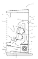
図2は、ファン付赤外線ストーブ1(以下、単にストーブ1と略称する)の断面概略図である。
ストーブ1は、前面に輻射開口2が設けられた本体ケース3内に、この輻射開口2に対向させて赤熱プレート式のバーナ4を備える。
【0020】
バーナ4は、燃料ガスと一次空気との混合室を形成するバーナ本体6と、バーナ本体6に装着される多数の炎孔が設けられたセラミックス製の燃焼プレート7とを備えた全一次空気式バーナであり、図示しない吸入孔から吸入された燃料ガスと一次空気とがバーナ本体6内で良好に混合され、その混合気が燃焼プレート7の炎孔から噴出して、燃焼プレート7上で表面燃焼する。
【0021】
また、バーナ本体6は、上バーナ本体13と下バーナ本体15とに上下二段で分割形成される。そして、燃焼プレート7は、上バーナ本体13と下バーナ本体15とにそれぞれ二枚ずつ設けられる構成であり、全面で燃焼する強火力設定と下バーナ本体15に設けられた二面のみで燃焼する弱火力設定の二種類の火力切替が行える。
【0022】
本体ケース3内の底部には、バーナ4の燃焼ガスを本体ケース3前面下部に設けられた温風吹出口8から送出するファン9が設けられる。バーナ4の後方には、バーナ4の上方近傍に燃焼ガス吸込口10を有し、ファン9に燃焼ガスと常温空気との混合気(温風)を導く温風吸気通路11が設けられる。そして、ファン9と温風吹出口8とは温風送出通路12によって連通される。
【0023】
また、器具背面上方で燃焼ガス吸込口10と略対向する位置に常温空気吸込口16が開口され、温風吸気通路11と連通される。従って、ファン9が駆動すると、燃焼ガス吸込口10から燃焼ガスが吸引され、常温空気吸込口16から室内の空気が吸引されて、温風吸気通路11及び温風送出通路12で混合され、燃焼ガスと外部空気の混合気が適度の温風として温風吹出口8から送出される。
【0024】
また、輻射開口2と温風吹出口8とには複数のガード棒14が設けられ、器具本体内に使用者の手等が入らないようになっている。
また、バーナ4の燃焼面5の前面に、前後二列で配列された直列型熱電対35が対向して設けられ、この熱電対35で得られた電力がファン9のモータ38の電源として用いられる。また、ファン9の左右には、熱電対35による発電を制御する熱発電制御装置30,乾電池32が設けられる(図2中の破線)。
【0025】
ファン9のモータ38には、DCブラシレスモータが用いられる。これは、ブラシモータが機械接点式で摩耗しやすく耐久性が悪いためである。このブラシレスモータ38は、内部にモータ38を回転制御するための集積回路であるIC38bを備えて、ICのトランジスタのスイッチングを短い周期で切り替える構成をしている。
【0026】
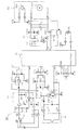
また、熱発電制御装置30は、図1に示されるように、主に、コントローラ31,乾電池32,点火スイッチ33,電源回路34,熱電対35,第1昇圧回路36,第2昇圧回路37,負荷駆動回路39等からなり、先ずこれらの構成および動作について説明する。尚、図中の符号CNはコネクタを示す。
【0027】
コントローラ31は、マイコンを主要部として構成され、熱発電制御,モータ駆動制御を行う。このコントローラ31の作動電圧は3Vで、耐電圧は5.5Vである。
点火スイッチ33は、乾電池32と電源回路34との接続スイッチで、点火レバーの点火操作に連動してオンになる。
熱電対35は、ストーブ1のバーナ4近傍に設けられ、火炎に加熱されて約1Vの起電力で電力を発生するもので、この電力がコントローラ31やモータ38の電源として利用される。
【0028】
第1昇圧回路36は、熱電対35で発生した起電力を昇圧するDC/DCコンバータで、その電力(電圧はVCC2)がモータ38の巻線38aへ供給され、モータ38を駆動させる。
この第1昇圧回路36は、コントローラ31の出力ポートcからのパルス信号によりオンオフするFET1(スイッチング素子),FET1のオンオフにより電圧を誘起するコイルL2,コイルL2の放電時のインピーダンスを小さくする電解コンデンサC3,電荷を蓄える電解コンデンサC4,昇圧後の電源(電解コンデンサC4や後述する電解コンデンサC7)から第1昇圧回路36側へ電流が流れることを防止するショットキーバリアーダイオードD3を備える。
【0029】
また、ショットキーバリアーダイオードD3は、電圧降下が0.2〜0.3Vと小さいもので、このダイオードでの消費電力を最低限に抑えており、発電した電力を効果的に負荷へ供給できる。
【0030】
こうした構成の第1昇圧回路36では、点火操作(点火スイッチ33のオン動作)から3秒経過後、熱電対35の起電力が所定値に達したとみなして、コントローラ31は、出力ポートcから周波数とデューティ比を調整したパルス信号をFET1へ送信し、そのパルス信号によりFET1をオンオフ動作させ、これによりコイルL2に電圧を誘起させて熱電対35からの入力電圧(1V)を昇圧して電気エネルギーを蓄えさせる。尚、この周波数とデューティ比の調整制御については後で詳述する。
【0031】
FET1がオンの時、熱電対35の起電力がコイルL2に電流を流す。FET1をオフすると、コイルL2の性質により電流を流し続けようとして電圧が上昇し、電流は、第1昇圧回路36と電源回路34との接続点Aを通って、第2昇圧回路37および負荷駆動回路39へ流れる。そして、この電流は、負荷駆動回路39からモータ38の巻線38aへの電源として使われる(この印加電圧はVCC2)。
この昇圧された電力がモータ38や、後述する負荷駆動回路39の疑似負荷40により消費されるため、第1昇圧回路36の出力電圧VCC2は、平均2.6Vとなる。コントローラ31は、その電圧を入力ポートbから検知する。
【0032】
第2昇圧回路37は、第1昇圧回路36で昇圧された出力電圧(2.6V)を更に所定電圧(3V)まで昇圧するDC/DCコンバータで、スイッチング素子となるFETを内蔵した第2昇圧回路37専用集積回路であるIC37aと、コイルL1と、電解コンデンサC2と、ダイオードD2とを備える。
この第2昇圧回路37は、パルス信号によりIC37aのFETをオンオフ動作させ、これによりコイルL1に電圧を誘起させて、後述する電源回路34や第1昇圧回路36からの入力電圧をVDD(3V)まで昇圧して、モータ38のIC38b(作動必要電圧は3V),コントローラ31の電源ポートd等へ電源として供給する。
【0033】
このように、コントローラ31の電源は、VCC2を用いずにVDD(第2昇圧回路37の出力)を用いている。これは、VCC2を用いた場合には、モータ38の巻線38aの負荷(必要電力)に影響を受けて印加電圧が不安定になってしまうからである。また、VCC2からでは、初期段階で第1昇圧回路36を駆動するために必要な電圧を得ることができないからである。
【0034】
この第2昇圧回路37のIC37aの電圧VDDは、コントローラ31およびモータ38のIC38bという軽い負荷(3V,0.1mAで0.3mW)しか接続されていないため、オンオフしても昇圧の変化が少なく安定している。一方、第1昇圧回路36の出力電圧VCC2は、モータ38という重い負荷(通常2.6V,160mAで416mW)に接続されるため、オンオフの度に昇圧の変化が大きく不安定になる。
このように、モータ38とコントローラ31とで印加電圧を分けているため、制御を司るコントローラ31に不安定な電圧が印加されることはなく、正常に制御を行うことができる。
【0035】
尚、第1昇圧回路36のFET1にはパワーMOSFETが用いられ、大きな電流を流すことができるが、第2昇圧回路37のIC37aは、FET1ほど大きな電流を流すことができないため、モータ38の巻線38aといった大きな負荷の駆動には適しておらず、コントローラ31やモータ38のIC38bといった負荷の小さい部品へ電力供給するための昇圧装置に用いられる。
【0036】
第1昇圧回路36からの電力を消費する負荷が大きい場合には、第1昇圧回路36の出力電圧VCC2は小さくなるので、入力ポートbの電圧Vbも低く、コントローラ31の故障の心配はない。
一方、負荷が小さい場合には、第1昇圧回路36の出力電圧VCC2は、10V程度になるため、入力ポートbの電圧Vbが高くなり過ぎてコントローラ31が故障してしまうおそれがあるが、抵抗R5,R6(各抵抗値は等しい)により入力電圧を半分に分圧しているため故障を防止できる。
【0037】
また、コントローラ31の過電圧による故障を防ぐために、入力ポートb(電圧検出部)には、入力ポートbへの印加電圧Vbを制限するダイオードD4が設けられ、このダイオードD4を介してVDDと接続される。このダイオードD4の電圧降下が0.7V程度と小さいため、仮に第1昇圧回路36で昇圧された起電力が非常に大きくなっても、入力ポートbの電圧Vbの最大値が、「VDD(3V)+0.7V」つまり3.7Vとなってコントローラ31が故障するおそれはない。
【0038】
熱電対35が発生する起電力では、モータ38を起動するために必要な電圧が得られないため、起電力を昇圧する必要があり、そのためには、第1昇圧回路36を作動させるコントローラ31へ電力を供給しなければならない。その電源として、乾電池32(電圧VCC1は1.5V)が用いられる。
【0039】
点火からしばらく経って、熱電対35が所定以上の起電力を発生するようになると、コントローラ31用の電力をその起電力で賄われるため、乾電池32からコントローラ31への電力供給を停止できる。
電源回路34は、この電力供給を遮断し、熱電対35からの電力供給に切り替える回路であり、コントローラ31によって制御される。
【0040】
この電源回路34は、乾電池電源の第2昇圧回路37への供給路を開閉するトランジスタQ1,トランジスタQ1のベースに制限抵抗R2を介して接続される電解コンデンサC1,電解コンデンサC1とトランジスタQ1のエミッタとの間に設けられる制限抵抗R1とダイオードD1,コントローラ31の出力ポートaに接続されると共に制限抵抗R2と電解コンデンサC1との間で接続されるデジタルトランジスタDT1,トランジスタQ1のコレクタに接続されるツェナーダイオードZD1を備える。
【0041】
R1は、放電時の過電流防止用の制限抵抗で、R2は、充電時の過電流防止用の制限抵抗である。また、ツェナーダイオードZD1は、コントローラ31への印加電圧がその耐電圧5.5Vを超えないようにしている。また、ダイオードD1は、点火スイッチ33をオフした時に、電解コンデンサC1に溜まった電荷を放出するために設けられ、これにより次回の点火時にも電解コンデンサC1をタイマー(後述)として用いることができる。
【0042】
電源回路34では、点火操作により点火スイッチ33がオンになると、乾電池32からの電流がトランジスタQ1のエミッタからベースへ流れてトランジスタQ1がオンになる。この電流は、制限抵抗R2,電解コンデンサC1へと流れる。
トランジスタQ1のオン動作に伴って、電流は、エミッタからコレクタ,第2昇圧回路37へ流れ、1.5Vから昇圧されて3V(VDD)となり、この出力電圧VDDがコントローラ31の電源として使用される。
【0043】
点火スイッチ33のオンから約10秒経過すると、電解コンデンサC1の電荷が溜まって、電解コンデンサC1に電流が流れなくなり、トランジスタQ1がオフになる。ここで、電解コンデンサC1はタイマーの働きをしている。
【0044】
次に、負荷駆動回路39について説明する。
負荷駆動回路39は、抵抗R7,R8からなる疑似負荷40と、コントローラ31の出力ポートeからの信号により疑似負荷40への通電を制御するデジタルトランジスタDT2と、コントローラ31の出力ポートfからの信号によりモータ38を駆動制御するFET2と、モータ38停止時の還流用のダイオードD5,セラミックコンデンサC8と、電解コンデンサC7と、FET2をオフするための抵抗R10とを備える。
【0045】
疑似負荷40は、モータ38を起動する時期が来るまで、つまり、熱電対35からの起電力が安定すると共に電解コンデンサC4,C7に電荷が溜まったとみなされるまで、昇圧された電力がモータ38の代わりに通電され、モータ38の駆動中は非通電状態になる。尚、疑似負荷40は、モータ38回転時の負荷抵抗よりもやや軽い。
【0046】
次に、コントローラ31が行う第1昇圧回路36での昇圧効率の調整制御について図3〜図5のフローチャートを用いて説明する。
前述したように、コントローラ31からFET1への制御信号の電圧と昇圧回路のオン抵抗(FET1のドレインとソースとの間の抵抗)とは反比例関係にあり、この電圧が大きいほどオン抵抗が小さく、昇圧時のエネルギー損失が少なくなって昇圧効率が高くなる。従って、ここでは、この電圧を大きくするように制御する。
【0047】
先ず、点火操作に連動して点火スイッチ33がオンになると、昇圧効率の制御を開始する。図3に示されるように、初期設定として、スイッチング周波数を6kHzに、デューティ比(1周期中のオン時間の割合)を70%とし(S1)、周波数を調整する際の増減を示す周波数変化符号を+に、デューティ比を調整する際の増減を示すデューティ比変化符号も+にする(S2)。
点火スイッチ33のオンから3秒経過するまで待機し(S3)、3秒経過後に周波数の調整処理(S4)、デューティ比の調整処理(S14)を繰り返して、出力電圧がピークに達するようにする。
【0048】
図4は、周波数の調整制御を示す。
先ず、入力ポートbで検出される現在のVCC2をV1として記憶する(S5)。尚、VCC2は抵抗R5,R6で半分に分圧されるため、例えば、入力ポートbで1.5Vが検出される場合には、その時のVCC2は3.0Vである。
そして、周波数変化符号が+の場合には周波数(ここでは6kHz)に0.25kHzを足し、周波数変化符号が−の場合には周波数から0.25kHzを引く(S6)。
周波数の変更から3秒経過するまで待機し(S7)、3秒経過後、電圧が安定したとみなして入力ポートbで現在のVCC2をV2として検出する(S8)。
【0049】
周波数変更前の電圧V1と変更後の電圧V2とを比較し(S9)、電圧V2が3.5V以下か否かを判断する(S10,S13)。
この判断値を3.5Vとしているのは、第2昇圧回路37の出力電圧VDDの上限を3V程度にするためであり、この結果、電圧V2が第2昇圧回路37の入力電圧を3.4V(ダイオードD2電圧降下0.4V+VDD)を極端に超えないようになる。
電圧V2が電圧V1を上回れば(S9:YES)、周波数の変更により昇圧した、つまり、昇圧効率が上がったことが分かる。
この際、電圧V2が3.5Vを超える場合には(S10:NO)、昇圧し過ぎによるコントローラ31(耐電圧5.5V)の故障を防止するため、周波数変化符号を今回と反対の符号にして(S12)、次回ステップ6に戻った時に降圧するようにしておく。つまり、+→−とし、−→+とする。
【0050】
一方、電圧V2が3.5V以下である場合には(S10:YES)、出力電圧が最大となるようにするために、周波数変化符号を今回と同じままにし(S11)、次回ステップ6に戻った時に更に昇圧するようにしておく。
そして、デューティ比を調整するサブルーチンへ移行する。
【0051】
ステップ9において、電圧V2が電圧V1以下であれば(S9:NO)、周波数の変更により降圧した、つまり、昇圧効率が下がったことが分かる。この際、電圧V2が3.5Vを超えていれば(S13:NO)、コントローラ31(耐電圧5.5V)が故障しないよう更に降圧させるために、周波数変化符号を今回と同じままにする(S11)。
一方、電圧V2が3.5V以下であれば(S13:YES)、出力電圧が最大となるように昇圧させるために、周波数変化符号を今回と反対の符号にする(S12)。
そして、デューティ比を調整するサブルーチンへ移行する。
【0052】
図5は、デューティ比の調整制御を示す。
先ず、入力ポートbで現在の電圧V1を記憶し(S15)、デューティ比変化符号が+の場合にはデューティ比(ここでは70%)に2%を足し、デューティ比変化符号が−の場合にはデューティ比から2%を引く(S16)。
デューティ比の変更から3秒経過するまで待機し(S17)、3秒経過後、電圧が安定したとみなして現在の電圧V2を検出する(S18)。
【0053】
デューティ比変更前の電圧V1と変更後の電圧V2とを比較し(S19)、電圧V2が3.5V以下か否かを判断する(S20,S23)。
電圧V2が電圧V1を上回れば(S19:YES)、デューティ比の変更により昇圧効率が上がったことが分かる。
この際、電圧V2が3.5V以下であれば(S20:YES)、更に昇圧するために、デューティ比変化符号を今回と同じままにし(S21)、電圧V2が3.5Vを超えれば(S20:NO)、これ以上昇圧させないために、デューティ比変化符号を今回と反対の符号にし(S22)、周波数を調整するサブルーチンに戻る。
【0054】
ステップ19において、電圧V2が電圧V1以下であれば(S19:NO)、デューティ比の変更により昇圧効率が下がったことが分かる。この際、電圧V2が3.5V以下であれば(S23:YES)、昇圧するために、デューティ比変化符号を今回と反対の符号にする(S22)。
一方、電圧V2が3.5Vを超えていれば(S23:NO)、コントローラ31(耐電圧5.5V)が故障しないよう更に降圧させるために、デューティ比変化符号を今回と同じままにする(S21)。
そして、周波数を調整するサブルーチンに戻る。
図3に示されるように、周波数の調整(S4)とデューティ比の調整(S14)とを交互に繰り返すことにより、出力電圧が最大ピークに近づいていき、昇圧効率が向上していく。
しかも、この出力電圧が3.5Vを超えることがないため、コントローラ31の故障を防止できる。
例えば、負荷の必要電力が小さい場合には、昇圧効率を無理して上げなくても負荷を駆動することができる。一方、負荷の必要電力が大きい場合には、昇圧効率を上げる必要があるが、コントローラ31の故障を招くほど昇圧しないように、第1昇圧回路36の出力電圧VCC2の上限値3.5Vを設定している。
【0055】
次に、電源回路34の制御について図6のフローチャートを用いて説明する。コントローラ31は、電解コンデンサC1によるタイマー終了前に(ここでは点火操作直後に)出力ポートaからデジタルトランジスタDT1をオンさせる(S31)。これにより、電流が乾電池32→トランジスタQ1のエミッタ→ベース→デジタルトランジスタDT1→乾電池32と流れ、タイマーに拘らずトランジスタQ1をオン状態に維持して、第2昇圧回路37を介して乾電池32によるコントローラ31への電力供給が継続される。この際、電解コンデンサC1に溜まっていた電荷は、デジタルトランジスタDT1へ向かって放出されて無くなる。
【0056】
熱電対35から所定値以上の起電力が発生し続けるようになると、乾電池32による電力供給の必要が無くなる。
そこで、コントローラ31は、抵抗R5,抵抗R6を用いて入力ポートbで電圧VCC2(=2Vb)を監視して(S32)、電圧VCC2が新品の乾電池32の電圧(1.8V)より大きい2.0V以上になったことを検出すると、熱電対35からの電力を乾電池32の代わりにコントローラ31の電源として用いることができるとみなして、出力ポートaからデジタルトランジスタDT1をオフさせる信号を送信する(S33)。
このデジタルトランジスタDT1のオフ動作により、再び電解コンデンサC1に電荷が溜まり始め、溜まりきるとトランジスタQ1に電流が流れなくなり、トランジスタQ1がオフとなって、乾電池32から第2昇圧回路37を介してコントローラ31への通電が停止される。従って、その後は熱電対35の起電力が第2昇圧回路37で昇圧されてコントローラ31の電源VDDとして使用される。
【0057】
ここで、コントローラ31による入力ポートbでの電圧Vbの検出について説明する。
昇圧前の熱電対35の起電力は、第1昇圧回路36のFET1および第2昇圧回路37のデジタルトランジスタDT1をオフさせることにより検出できる。
また、第1昇圧回路で昇圧された電圧は、第2昇圧回路37のデジタルトランジスタDT1をオフさせることにより検出できる。また、このデジタルトランジスタDT1をオフさせなくても、検出値が新品の乾電池32の電圧1.8Vを超えていれば、第1昇圧回路36で起電力を昇圧した電圧として検出できる。
また、乾電池32の電圧は、第2昇圧回路37のデジタルトランジスタDT1をオンさせることにより検出できる。
【0058】
コントローラ31は、熱電対35の起電力により第2昇圧回路37を介して電源供給されている時に、入力ポートbで電圧VCC2が新品の乾電池32の電圧1.8V以下になったことを検出すると(S34:YES)、出力ポートaからデジタルトランジスタDT1をオンさせる信号を送信し(S35)、電源回路34を作動させて乾電池32から第2昇圧回路37を介して電力を受ける。従って、突風等により熱電対35の起電力が突然下がっても乾電池32から電力を供給をするため、コントローラ31の作動が停止してしまうことがない。
【0059】
しかも、入力ポートbで電圧VCC2が1.8V以下の状態が5分間継続した場合には(S36:YES)、コントローラ31は、バーナ4が立ち消えしているとみなして、出力ポートaからデジタルトランジスタDT1をオフさせる信号を送信し(S37)、電源回路34を停止して乾電池32からの電力供給を停止する。この際、熱電対35からも電力が供給されないため、コントローラ31やモータ38は停止する。
一方、乾電池32による電力供給時に、電圧VCC2が1.8V以下の状態が5分間継続せずに途中で1.8Vを上回った場合には(S36:NO)、ステップ32へ戻って、再び電圧VCC2の監視を行う。
【0060】
次に、モータ38の駆動のタイミングについて説明する。
コントローラ31には、モータ38の駆動のタイミングを決定する2つのタイマーが設けられる。一方のタイマーが、第1昇圧回路36の出力電圧VCC2が2.2V以上である状態が30秒間継続したこと(第1条件)を検出し、かつ、他方のタイマーが、点火スイッチ33のオンから2分経過したこと(第2条件)を検出すると、熱電対35の起電力が安定したとみなされ、この起電力を利用してモータ38の駆動を開始する。
【0061】
しかしながら、モータ38は、始動時の負荷が非常に重いため、熱電対35の起電力をそのまま昇圧するだけでは、回転を始めることができない。
そこで、熱電対35から発生した電荷を電解コンデンサC4とC7で一旦溜めてからモータ38へ電力を供給することにより、モータ38を停止状態から一気に回転させることができる。尚、この時の印加電圧は、約3.5Vである。また、このモータ38の起動直後であっても、第2昇圧回路37では、電力をダイオードD2で消費するため、その出力電圧が3.2V程度となり、コントローラ31を故障させる心配はない。
【0062】
このモータ38の駆動制御について図7のフローチャートを用いて説明する。点火操作直後はデジタルトランジスタDT2をオンして(S41)、熱電対35からの昇圧電圧VCC2を疑似負荷40に通電し、電解コンデンサC4,C7に電荷を溜める。
【0063】
そして、コントローラ31内の2つのタイマーがそれぞれ、第1昇圧回路36の出力電圧VCC2が2.2V以上である状態が30秒間継続したこと(第1条件)を検出し(S42:YES)、かつ、点火スイッチ33のオンから2分経過したこと(第2条件)を検出する(S43:YES)と、熱電対35の起電力が安定し、かつ、電解コンデンサC4,C7に電荷が溜まったとみなされる。
【0064】
そして、デジタルトランジスタDT2をオフして(S44)、疑似負荷40の通電を停止すると共に、FET2をオンに切り替えて(S45)、モータ38の通電を開始する。この起動時のモータ38の電源電圧は約3Vである。
【0065】
回転し始めたモータ38は、以降大きな電力を必要としないため、電解コンデンサC4,C7に電荷をたくさん溜めなくても、熱電対35の起電力を昇圧した電圧(2.6V)のまま、モータ38を駆動し続けることができる。
【0066】
モータ38の駆動中、第1昇圧回路36の出力電圧VCC2が2.0V以下になった場合には(S46:YES)、必要な電圧が得られないため、FET2をオフして(S47)、モータ38の駆動を停止させる。
モータ38の駆動中に、電圧VCC2が2.0V以下になると、FET2をオフに切り替えて、モータ38の通電を停止する。
【0067】
このように、電解コンデンサC4とC7で蓄電してからモータ38へ電力を供給するため、熱電対38が大きな電力を発生しなくても、モータ38を起動することができる。従って、発電量の多い熱電対を用いる必要がなく、熱電対の製造コストを安価に抑えることができる。
【0068】
また、モータ38の駆動タイミングの第2条件(通電開始から2分経過すること)により、熱電対35の起電力が安定するまで待機するため、各電解コンデンサC4,C7に確実に電荷を溜めることができる。
【0069】
また、モータ38の駆動タイミングの第1条件(第1昇圧回路36の出力電圧が2.2V以上である状態が30秒間継続すること)により、第1昇圧回路36から十分な出力電圧が得られるため、第2条件からは把握できないバーナ4の点火失敗などによる起電力不足を判断でき、熱電対35が実際に発電していることを確認した上でモータ38を駆動させることができる。
しかも、出力電圧が所定値以上であることを条件にすることに加えて、その状態を所定時間継続することも条件としているため、第1昇圧回路36の出力電圧が一時的に2.2V以上になってもモータ38の駆動を開始せず、必要電力が蓄えられるまで待機する。この結果、一層確実にモータ駆動のための電力を蓄えることができる。
【0070】
このモータ駆動制御中においても、昇圧効率の調整制御は同時に行われており、疑似負荷40に通電中は、疑似負荷40に合わせて周波数やデューティ比を調整することにより、昇圧効率の調整制御を行う。
この昇圧効率の調整制御で出力電圧が最大になっていない場合でも、ステップ46においてモータ38に通電されれば、今度はモータ38に合わせて周波数やデューティ比を調整することにより、昇圧効率の調整制御を行う。
【0071】
このように、モータ38の通電を開始する時には、ある程度モータ負荷に合った昇圧効率に調整されているため、モータ38は、疑似負荷40用に調整された電圧が起動時に印加され、確実に駆動を開始することができる。
【0072】
仮に疑似負荷が設けられない場合には、モータ38の通電前に電力が疑似負荷で消費されないので、昇圧効率を最適値にするために調整される周波数やデューティ比がモータ38の通電前と通電後とでは大きく異なり、第1昇圧回路36の出力電圧も急激に低下してしまう。従って、モータ38の通電直後にモータ38に印加される電圧が低過ぎて、モータ38が停止してしまう。
これに対して、本実施形態では、モータ38とほぼ等しい負荷抵抗を持つ疑似負荷40を用い、モータ38始動前に予め昇圧効率を調整するため、このような不具合は生じない。
【0073】
そして、モータ38の起動後も周波数の調整とデューティ比の調整とを繰り返すことにより、この発電した電力を適切な電圧でモータ38へ安定して供給することができる。モータ38に風が入り込む等によりモータ38の負荷が変動しても、その必要電力に応じて周波数とデューティ比との交互制御を行い昇圧効率を調整する。
こうした周波数やデューティ比は、部品のばらつきや、周囲の温度、負荷の大きさにより変化するが、出力電圧をフィードバックしつつ(図4のS9や図5のS19)、周波数やデューティ比を繰り返し制御することで、正確に出力電圧を制御できる。
【0074】
こうしたモータ38は高周波ノイズを発生するが、この高周波ノイズ対策として、第1昇圧回路36と入力ポートbとの間には、セラミックコンデンサC5,C6が設けられる。
【0075】
コントローラ32には、乾電池32の消耗を使用者に報知するLEDが接続され、熱電対35の発電前に、乾電池32の電圧を入力ポートbで確認し、その電圧が1.1V未満となった場合には、LEDを点灯する。
【0076】
次に、昇圧効率とスイッチング素子との関係について説明する。
昇圧効率は、第1昇圧回路36のスイッチング素子(FET1)の特性により大きな影響を受ける。熱電対35から取り出すことができる電力Wは、熱電対35の開放電圧をV,熱電対35の内部抵抗をR,熱電対35に接続された熱電対回路全体の負荷(モータ38を含む)の抵抗をr,その熱電対回路を流れる電流をIとすると、
W=I2rにI=V/(R+r)を代入して、
W=V2r/(R+r)2となる。この式をrで微分して最大値を求めると、熱電対35から取り出し可能な電力Wは、r=Rの場合に最大になる。
【0077】
例えば、熱電対を複数合わせて発電する場合に、その熱電対35の内部抵抗Rは0.5Ωと小さいため、ここからその電力を昇圧して大きな電力を取り出すためには、r=R(つまりr=0.5Ω)に近づける必要があり、昇圧回路のインピーダンスを小さく抑える必要がある。
そのためには、スイッチングを行う素子(パワーMOSFET、つまりFET1)のオン抵抗を低くすることが必要となり、FET1のゲート電圧(入力電圧)をある程度高くする必要がある。
【0078】
仮に、第1昇圧回路36で昇圧した出力電力VCC2をコントローラ31の電源として用いた場合には、その電圧は、負荷変動により変化するため、一旦、昇圧電圧が低くなると、スイッチング素子のオン特性が悪化し、更に昇圧効率が下がって昇圧電圧が下がるという悪循環に陥ってしまう。
そこで、本実施形態では、昇圧効率に大きな影響を与えるスイッチング素子には、メインの負荷(モータ38)の昇圧回路(第1昇圧回路36)とは別の昇圧回路(第2昇圧回路37)にて昇圧した電源が用いられ、電圧の安定化を図っている。
【0079】
上述した熱発電制御装置30では、第1昇圧回路36が熱電対35の起電力を昇圧するため、熱電対を多数接続することにより高い起電力を発生しなくてもモータ38を起動でき、熱電対の製造コストが安価となる。
【0080】
次に昇圧効率について説明する。モータ38の巻線38aに必要な電圧は、2.6Vであり、コントローラ31やIC38bと同じ電圧(3V)にする必要がない。
例えば、1Vから3Vへ昇圧したい場合には、一気に1Vから3Vへ昇圧させようとする場合に、昇圧差が大き過ぎて3Vまで十分昇圧できないことが起こり得る。これに対して、先ず第1昇圧回路36が1Vから2.6Vまで余裕を持って昇圧し、次に第2昇圧回路27がこの2.6Vを3Vまで確実に昇圧する。
このように2段階に分けて昇圧することで無理なく、所望の電圧まで昇圧することができる。
しかも、昇圧差が大きいほどエネルギー損失の増加により昇圧効率が低下するため、IC38bの印加電圧VDD(3V)用の昇圧回路(第2昇圧回路37)と、巻線38aの印加電圧VCC2(2.6V)用の昇圧回路(第1昇圧回路36)とを分けることにより、巻線38aでの昇圧効率は、昇圧目標値を3Vとする場合よりも良くなる。
これらの結果、発電した電力を有効に利用することができる。
【0081】
また、熱発電制御装置30では、コントローラ31への電力供給源を乾電池32から熱電対35に切り替えるため、乾電池32を無駄に消費することがなく、長期に渡って乾電池32を使用することができる。このため、乾電池交換を頻繁に行う必要もない。
【0082】
以上本発明の実施形態について説明したが、本発明はこうした実施形態に何等限定されるものではなく、本発明の要旨を逸脱しない範囲において、種々なる態様で実施し得ることは勿論である。
例えば、昇圧効率の調整制御において、周波数とデューティ比とを交互に何度も調整するのではなく、周波数とデューティ比とをそれぞれ1回ずつ調整してもよい。
また、起動時のモータへの印加電圧を高くするために、疑似負荷40の負荷抵抗をモータ38の負荷抵抗の半分程度にするなど比較的小さくしてもよい。
また、モータ38の駆動のタイミングを第1条件「第1昇圧回路36の出力電圧が2.2V以上である状態が30秒間継続したこと」と第2条件「点火スイッチ33のオンから2分経過したこと」との両方を満足した時とすることに代えて、第1条件を満たした時としてもよいし、また、第2条件を満たした時としてもよい。
【0083】
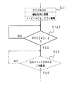
また、モータ38の駆動のタイミングの第1条件のように所定時間(例えば30秒)待機すること(S42)に代えて、図8に示されるように、第1昇圧回路36の出力電圧が所定電圧(例えば2.2V)以上であること(S142)を条件としてもよい。
また、モータ38の駆動のタイミングの第2条件の計時開始条件を点火操作時ではなく、第1昇圧回路36の作動開始時としてもよく、このように点火操作に伴う事象を捉えたタイミングであればよい。
【0084】
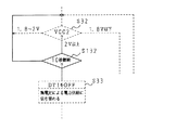
また、コントローラ31への電力供給源を乾電池32の電力から熱電対35の発電電力に切り替えるタイミングを、第1昇圧回路36の出力電圧が所定電圧以上に達した時とするのではなく、この状態が所定時間継続した時としてもよい。例えば、図9に示されるように、図6のS32でVCC2が2V以上と判断された場合に、S132のように、その状態が10秒継続した時に、乾電池から熱電対にコントローラ31への電力供給源を切り替えてもよい。
この場合では、熱電対35の起電力の一時的な上昇に影響されることなく、熱電対35から第1昇圧回路36を介してコントローラ31に必要作動電力を供給できるようになるまで乾電池32から電力供給を行うため、一層確実にコントローラ31の作動を継続することができる。
【0085】
【発明の効果】
以上詳述したように、本発明の請求項1の熱発電制御装置によれば、熱発電素子の起電力の昇圧効率を調整して、発電した電力を負荷へ供給するため、負荷を安定して駆動することができる。
しかも、昇圧効率が調整されるため、発電エネルギーを有効に利用できる。
更に、昇圧効率制御回路の電源用の電力を負荷の電源用の電力から分けて第2昇圧回路で昇圧するため、昇圧効率制御回路の作動が安定し、昇圧効率を適切に調整でき、発電した電力を有効に利用できる。
また、負荷で必要電力が変動しても、昇圧効率制御回路には、負荷とは異なる安定した電圧が印加されるため、高い昇圧効率で負荷を安定して駆動できる。
【0086】
更に、本発明の請求項2の熱発電制御装置によれば、モータの駆動前に予め昇圧効率を疑似負荷の必要電力に応じて仮調整しておくため、モータ駆動時に昇圧効率が極端に変化せず、モータへの出力電圧の急低下によるモータの不作動を防止できる。
【0087】
更に、本発明の請求項3の熱発電制御装置によれば、熱発電素子の起電力の昇圧効率を調整して、発電した電力を負荷へ供給するため、負荷を安定して駆動することができる。
しかも、昇圧効率が調整されるため、発電エネルギーを有効に利用できる。
更に、モータの駆動前に予め昇圧効率を疑似負荷の必要電力に応じて仮調整しておくため、モータ駆動時に昇圧効率が極端に変化せず、モータへの出力電圧の急低下によるモータの不作動を防止できる。
【図面の簡単な説明】
【図1】本実施形態としての熱発電制御回路図である。
【図2】本実施形態としてのファン付赤外線ストーブの断面概略図である。
【図3】本実施形態としての第1昇圧回路での昇圧効率の調整制御を示したフローチャートである。
【図4】本実施形態としての周波数の調整制御を示したフローチャートである。
【図5】本実施形態としてのデューティ比の調整制御を示したフローチャートである。
【図6】本実施形態としての電源回路の制御を示したフローチャートである。
【図7】本実施形態としてのモータ駆動制御を示したフローチャートである。
【図8】変更例としてのモータ駆動制御を示したフローチャートである。
【図9】変更例としての電源回路の制御を示したフローチャートである。
【符号の説明】
1…ストーブ、4…バーナ、9…ファン、30…熱発電制御装置、31…コントローラ、32…乾電池、33…点火スイッチ、34…電源回路、35…熱電対、36…第1昇圧回路、37…第2昇圧回路、37a…IC、38…モータ、38a…巻線、38b…IC、40…疑似負荷、FET1…スイッチング素子、L2…コイル、C1〜C4,C7…電解コンデンサ、b…入力ポート、d…電源ポート。[0001]
BACKGROUND OF THE INVENTION
The present invention relates to a thermoelectric generator control device that boosts and controls an electromotive force from a thermoelectric generator such as a thermocouple.
[0002]
[Prior art]
2. Description of the Related Art Conventionally, there is known a thermoelectric generation control device that boosts an electromotive force of a thermocouple heated by a burner with a booster circuit and drives an actuator such as a fan motor with the boosted output voltage.
As an example of application of such a thermoelectric generation control device to an infrared heater, an infrared heater with a fan that performs heating by hot air from a blower fan driven by thermoelectric generation in addition to radiant heat from a red-hot plate type gas burner is known. .
[0003]
[Problems to be solved by the invention]
However, since the energy generated by the thermocouple is unstable, the boosted voltage is also unstable. Moreover, the boosted output voltage is affected by the size of the load, and the output is not stable. For this reason, the stable operation | movement of loads, such as a ventilation fan, was not obtained.
The thermoelectric power generation control device of the present invention has an object to solve the above-described problems and to control the electric power generated by the thermoelectric generator to stably supply it to a load.
[0004]
[Means for Solving the Problems]
The thermoelectric power generation control device according to
A thermoelectric generator that generates electricity by heat;
A booster circuit for inducing a voltage in the coil by turning on and off the switching element to boost the electromotive force input from the thermoelectric generator;
A load energizing circuit for energizing the load using the boosted power as a power source;
Voltage detection means for detecting the power supply voltage of the load;
A step-up efficiency control circuit for adjusting the step-up efficiency by controlling the switching element so that the output voltage of the step-up circuit, which is a detection voltage of the voltage detection means, is maximized;,
A second booster circuit for further boosting the output voltage boosted by the booster circuit;
The power boosted by the second booster circuit is used as a power source for the boosting efficiency control circuitThis is the gist.
[0005]
Moreover, the thermoelectric generation control device according to
The load is a motor,
A pseudo load that consumes the boosted electromotive force instead of the motor is provided, and before the motor is driven, the pseudo load is energized so that the power supply voltage of the pseudo load is maximized. Temporarily adjustedThis is the gist.
[0006]
A thermoelectric generator control device according to
A thermoelectric generator that generates electricity by heat;
A booster circuit for inducing a voltage in the coil by turning on and off the switching element to boost the electromotive force input from the thermoelectric generator;
A load energizing circuit for energizing the motor using the boosted power as a power source;
Voltage detection means for detecting the power supply voltage of the motor;
A step-up efficiency control circuit for adjusting the step-up efficiency by controlling the switching element so that the output voltage of the step-up circuit, which is the detection voltage of the voltage detection means, is maximized;
A pseudo load that consumes electric power obtained by boosting the electromotive force instead of the motor;
Before driving the motor, the boosting efficiency is temporarily adjusted by energizing the pseudo load and maximizing the power supply voltage of the pseudo load.This is the gist.
[0011]
In the thermoelectric generation control device according to
The boosting efficiency is a ratio (in this case, 2.4 W / 3 W = 80%) of electric power (eg, 2.4 V at 6 V, 0.4 A) obtained by boosting from a power source (eg, 3 V at 1 A). is there.
Further, the electromotive force is boosted by the booster circuit and used as a power source for the load, and the output voltage boosted by the booster circuit is further boosted by the second booster circuit and used as the power source for the boosting efficiency control circuit.
For example, when boosting from 1 V to 3 V, when boosting from 1 V to 3 V at a stretch, it is possible that the boosting difference is too large and can only be boosted to about 2.7 V. On the other hand, when the booster circuit first boosts the voltage from 1V to 2.6V with a margin, and then the second booster circuit boosts the boosted 2.6V to 3V, it is surely desired. The voltage can be boosted to a voltage.
By the way, the voltage of the control signal from the boosting efficiency control circuit and the on-resistance of the boosting circuit are inversely proportional to each other. The larger the signal voltage, the smaller the on-resistance, and the lower the energy loss during boosting and the higher the boosting efficiency. Therefore, by raising the power supply voltage of the boosting efficiency control circuit to the second boosting circuit, the operation of the boosting efficiency control circuit is stabilized and the boosting efficiency can be adjusted reliably.
[0012]
A thermoelectric generator control device according to
[0013]
A thermoelectric generator control device according to
The boosting efficiency is a ratio (in this case, 2.4 W / 3 W = 80%) of electric power (eg, 2.4 V at 6 V, 0.4 A) obtained by boosting from a power source (eg, 3 V at 1 A). is there.
Furthermore, before the motor is driven, the boosted power is applied to a pseudo load such as a resistor instead of the motor. During this time, the boosting efficiency is temporarily adjusted so that the power supply voltage at the pseudo load is maximized, so that the boosting efficiency is adjusted to some extent even if the energization to the pseudo load is stopped and the motor is driven. For this reason, the output voltage does not drop abruptly when the motor is energized, and the motor is prevented from rotating.
[0018]
DETAILED DESCRIPTION OF THE INVENTION
In order to further clarify the configuration and operation of the present invention described above, a preferred embodiment of the thermoelectric generator control apparatus of the present invention will be described below.
[0019]
A thermoelectric generator control device as one embodiment of the present invention will be described with reference to FIGS.
FIG. 2 is a schematic cross-sectional view of an
The
[0020]
The burner 4 includes a
[0021]
The
[0022]
A fan 9 is provided at the bottom of the
[0023]
In addition, a room
[0024]
In addition, a plurality of
Further, series-
[0025]
A DC brushless motor is used as the
[0026]
As shown in FIG. 1, the thermoelectric
[0027]
The
The
The
[0028]
The
The
[0029]
In addition, the Schottky barrier diode D3 has a small voltage drop of 0.2 to 0.3 V, suppresses the power consumption of this diode to the minimum, and can effectively supply the generated power to the load.
[0030]
In the
[0031]
When FET1 is on, the electromotive force of the
Since the boosted electric power is consumed by the
[0032]
The
The
[0033]
Thus, the power supply of the
[0034]
The voltage VDD of the
As described above, since the applied voltage is divided between the
[0035]
The
[0036]
When the load that consumes the power from the
On the other hand, when the load is small, the output voltage VCC2 of the
[0037]
In addition, in order to prevent a failure due to an overvoltage of the
[0038]
In the electromotive force generated by the
[0039]
When the
The
[0040]
The
[0041]
R1 is a limiting resistor for preventing overcurrent during discharging, and R2 is a limiting resistor for preventing overcurrent during charging. In addition, the Zener diode ZD1 prevents the voltage applied to the
[0042]
In the
Along with the ON operation of the transistor Q1, the current flows from the emitter to the collector and the
[0043]
When about 10 seconds elapse after the
[0044]
Next, the
The
[0045]
The
[0046]
Next, boosting efficiency adjustment control in the first boosting
As described above, the voltage of the control signal from the
[0047]
First, when the
Wait until 3 seconds have elapsed since the
[0048]
FIG. 4 shows frequency adjustment control.
First, the current VCC2 detected at the input port b is stored as V1 (S5). Since VCC2 is divided in half by resistors R5 and R6, for example, when 1.5V is detected at input port b, VCC2 at that time is 3.0V.
When the frequency change code is +, 0.25 kHz is added to the frequency (here, 6 kHz), and when the frequency change code is-, 0.25 kHz is subtracted from the frequency (S6).
Wait until 3 seconds have passed since the frequency change (S7), and after 3 seconds, assume that the voltage has stabilized and detect the current VCC2 as V2 at the input port b (S8).
[0049]
The voltage V1 before the frequency change and the voltage V2 after the change are compared (S9), and it is determined whether or not the voltage V2 is 3.5 V or less (S10, S13).
The reason why the determination value is 3.5 V is that the upper limit of the output voltage VDD of the
If the voltage V2 exceeds the voltage V1 (S9: YES), it can be seen that the voltage has been boosted by changing the frequency, that is, the boosting efficiency has increased.
At this time, if the voltage V2 exceeds 3.5V (S10: NO), in order to prevent the controller 31 (withstand voltage 5.5V) from being damaged due to excessive boosting, the frequency change code is set to the opposite sign to that of this time. (S12), the pressure is stepped down when the process returns to step 6 next time. That is, + → − and − → +.
[0050]
On the other hand, when the voltage V2 is 3.5 V or less (S10: YES), the frequency change code is kept the same as this time (S11) to return to the maximum output voltage, and the
Then, the process proceeds to a subroutine for adjusting the duty ratio.
[0051]
In step 9, if the voltage V2 is equal to or lower than the voltage V1 (S9: NO), it is found that the voltage has been stepped down by changing the frequency, that is, the step-up efficiency has decreased. At this time, if the voltage V2 exceeds 3.5V (S13: NO), the frequency change code remains the same as this time in order to further reduce the controller 31 (withstand voltage 5.5V) so as not to fail ( S11).
On the other hand, if the voltage V2 is 3.5 V or less (S13: YES), in order to boost the output voltage so as to maximize, the frequency change code is changed to a code opposite to this time (S12).
Then, the process proceeds to a subroutine for adjusting the duty ratio.
[0052]
FIG. 5 shows duty ratio adjustment control.
First, the current voltage V1 is stored at the input port b (S15). When the duty ratio change code is +, 2% is added to the duty ratio (70% here), and when the duty ratio change code is-.
It waits until 3 seconds elapse from the change of the duty ratio (S17), and after 3 seconds elapses, the voltage is considered stable and the current voltage V2 is detected (S18).
[0053]
The voltage V1 before the duty ratio change and the voltage V2 after the change are compared (S19), and it is determined whether or not the voltage V2 is 3.5 V or less (S20, S23).
If the voltage V2 exceeds the voltage V1 (S19: YES), it can be seen that the boosting efficiency is increased by changing the duty ratio.
At this time, if the voltage V2 is 3.5V or less (S20: YES), in order to further boost the voltage, the duty ratio change code is kept the same as this time (S21), and if the voltage V2 exceeds 3.5V (S20). : NO), in order not to boost the pressure any more, the duty ratio change code is changed to the opposite sign (S22), and the process returns to the subroutine for adjusting the frequency.
[0054]
In
On the other hand, if the voltage V2 exceeds 3.5V (S23: NO), the duty ratio change code remains the same as this time in order to further step down the controller 31 (withstand voltage 5.5V) so as not to fail ( S21).
Then, the process returns to the subroutine for adjusting the frequency.
As shown in FIG. 3, by alternately repeating the frequency adjustment (S4) and the duty ratio adjustment (S14), the output voltage approaches the maximum peak, and the boosting efficiency is improved.
Moreover, since the output voltage does not exceed 3.5V, failure of the
For example, when the required power of the load is small, the load can be driven without forcibly increasing the boosting efficiency. On the other hand, when the required power of the load is large, it is necessary to increase the boosting efficiency, but the upper limit value 3.5V of the output voltage VCC2 of the
[0055]
Next, control of the
[0056]
When an electromotive force of a predetermined value or more continues to be generated from the
Therefore, the
Due to the turning-off operation of the digital transistor DT1, electric charge begins to accumulate again in the electrolytic capacitor C1, and when the accumulation is completed, no current flows through the transistor Q1, the transistor Q1 is turned off, and the
[0057]
Here, detection of the voltage Vb at the input port b by the
The electromotive force of the
The voltage boosted by the first booster circuit can be detected by turning off the digital transistor DT1 of the
The voltage of the
[0058]
When the
[0059]
In addition, when the state where the voltage VCC2 is 1.8 V or less at the input port b continues for 5 minutes (S36: YES), the
On the other hand, when power is supplied by the
[0060]
Next, the driving timing of the
The
[0061]
However, since the load at the start of the
Therefore, the electric charge generated from the
[0062]
The drive control of the
[0063]
Then, the two timers in the
[0064]
Then, the digital transistor DT2 is turned off (S44), the energization of the
[0065]
Since the
[0066]
When the output voltage VCC2 of the
If the voltage VCC2 becomes 2.0 V or less during driving of the
[0067]
As described above, since the electric power is supplied to the
[0068]
In addition, because the second condition of the drive timing of the motor 38 (2 minutes from the start of energization) waits until the electromotive force of the
[0069]
Further, a sufficient output voltage can be obtained from the
Moreover, in addition to the condition that the output voltage is equal to or higher than a predetermined value, the condition that the state is continued for a predetermined time is also a condition. Therefore, the output voltage of the
[0070]
Even during the motor drive control, the boost efficiency adjustment control is performed simultaneously. While the
Even if the output voltage is not maximized by this boosting efficiency adjustment control, if the
[0071]
In this way, when energization of the
[0072]
If a pseudo load is not provided, electric power is not consumed by the pseudo load before the
On the other hand, in the present embodiment, such a problem does not occur because the
[0073]
The generated power can be stably supplied to the
Such frequency and duty ratio vary depending on component variations, ambient temperature, and load size, but the frequency and duty ratio are repeatedly controlled while feeding back the output voltage (S9 in FIG. 4 and S19 in FIG. 5). By doing so, the output voltage can be accurately controlled.
[0074]
Such a
[0075]
The
[0076]
Next, the relationship between the boosting efficiency and the switching element will be described.
The step-up efficiency is greatly affected by the characteristics of the switching element (FET 1) of the first step-up
W = I2Substituting I = V / (R + r) for r,
W = V2r / (R + r)2It becomes. When this equation is differentiated by r to obtain the maximum value, the electric power W that can be taken out from the
[0077]
For example, when power is generated by combining a plurality of thermocouples, the internal resistance R of the
For this purpose, it is necessary to lower the on-resistance of the element that performs switching (power MOSFET, that is, FET1), and it is necessary to increase the gate voltage (input voltage) of FET1 to some extent.
[0078]
If the output power VCC2 boosted by the
Therefore, in the present embodiment, a switching element that has a large effect on the boosting efficiency is connected to a booster circuit (second booster circuit 37) different from the booster circuit (first booster circuit 36) of the main load (motor 38). A boosted power supply is used to stabilize the voltage.
[0079]
In the thermoelectric
[0080]
Next, the boosting efficiency will be described. The voltage required for the winding 38a of the
For example, when it is desired to boost from 1V to 3V, when trying to boost from 1V to 3V at once, the boosting difference may be too large to be sufficiently boosted to 3V. On the other hand, the
Thus, by boosting in two stages, it is possible to boost to a desired voltage without difficulty.
In addition, since the boosting efficiency decreases due to an increase in energy loss as the boosting difference increases, the booster circuit (second booster circuit 37) for the applied voltage VDD (3V) of the
As a result, the generated power can be used effectively.
[0081]
Further, in the thermoelectric
[0082]
Although the embodiment of the present invention has been described above, the present invention is not limited to such an embodiment, and it is needless to say that the present invention can be implemented in various modes without departing from the gist of the present invention.
For example, in the adjustment control of the boost efficiency, the frequency and the duty ratio may be adjusted once instead of adjusting the frequency and the duty ratio alternately and repeatedly.
Further, in order to increase the voltage applied to the motor at the time of startup, the load resistance of the
In addition, the driving timing of the
[0083]
Further, instead of waiting for a predetermined time (for example, 30 seconds) as in the first condition of the driving timing of the motor 38 (S42), as shown in FIG. 8, the output voltage of the
In addition, the timing start condition of the second condition of the driving timing of the
[0084]
The timing for switching the power supply source to the
In this case, from the
[0085]
【The invention's effect】
As described above in detail, according to the thermoelectric generator control device of the first aspect of the present invention, the boosting efficiency of the electromotive force of the thermoelectric generator is adjusted and the generated electric power is supplied to the load. Can be driven.
In addition, since the boosting efficiency is adjusted, the generated power can be used effectively.
Furthermore, the power for the boosting efficiency control circuit is divided from the power for the power supply of the load and boosted by the second boosting circuit, so that the operation of the boosting efficiency control circuit is stable, the boosting efficiency can be adjusted appropriately, and power is generated. Electricity can be used effectively.
Even if the required power fluctuates with the load, a stable voltage different from the load is applied to the boosting efficiency control circuit, so that the load can be stably driven with high boosting efficiency.
[0086]
Furthermore, according to the thermoelectric generation control device of
[0087]
Furthermore, according to the thermoelectric generation control device of
In addition, since the boosting efficiency is adjusted, the generated power can be used effectively.
Furthermore, since the boosting efficiency is temporarily adjusted in advance according to the required power of the pseudo load before the motor is driven, the boosting efficiency does not change drastically when the motor is driven, and the motor is not affected by a sudden drop in the output voltage to the motor. Operation can be prevented.
[Brief description of the drawings]
FIG. 1 is a thermoelectric generation control circuit diagram according to the present embodiment.
FIG. 2 is a schematic cross-sectional view of a fan-equipped infrared heater as the present embodiment.
FIG. 3 is a flowchart showing boosting efficiency adjustment control in the first booster circuit according to the present embodiment;
FIG. 4 is a flowchart illustrating frequency adjustment control according to the present embodiment.
FIG. 5 is a flowchart showing duty ratio adjustment control according to the present embodiment;
FIG. 6 is a flowchart showing control of a power supply circuit according to the present embodiment.
FIG. 7 is a flowchart showing motor drive control as the embodiment.
FIG. 8 is a flowchart showing motor drive control as a modified example.
FIG. 9 is a flowchart showing control of a power supply circuit as a modified example.
[Explanation of symbols]
DESCRIPTION OF
Claims (3)
スイッチング素子のオンオフによりコイルに電圧を誘起させて、上記熱発電素子から入力された起電力を昇圧させる昇圧回路と、
昇圧された電力を電源として負荷に通電する負荷通電回路と、
上記負荷の電源電圧を検出する電圧検出手段と、
上記電圧検出手段の検出電圧である上記昇圧回路の出力電圧が最大となるように上記スイッチング素子を制御して昇圧効率を調整する昇圧効率制御回路と、
上記昇圧回路で昇圧された出力電圧を更に昇圧させる第2昇圧回路と
を備え、上記第2昇圧回路で昇圧された電力を上記昇圧効率制御回路の電源として用いることを特徴とする熱発電制御装置。A thermoelectric generator that generates electricity by heat;
A booster circuit for inducing a voltage in the coil by turning on and off the switching element to boost the electromotive force input from the thermoelectric generator;
A load energizing circuit for energizing the load using the boosted power as a power source;
Voltage detection means for detecting the power supply voltage of the load;
A step-up efficiency control circuit for adjusting the step-up efficiency by controlling the switching element so that the output voltage of the step-up circuit, which is the detection voltage of the voltage detection means, is maximized ;
A second booster circuit for further boosting the output voltage boosted by the booster circuit;
And the electric power boosted by the second booster circuit is used as a power source of the boosting efficiency control circuit .
上記起電力を昇圧した電力を上記モータの代わりに消費する疑似負荷を設け、該モータを駆動する前に、該疑似負荷に通電して該疑似負荷の電源電圧が最大となるように昇圧効率を仮調整するようにしたことを特徴とする請求項1記載の熱発電制御装置。 The load is a motor,
A pseudo load that consumes the boosted electromotive force instead of the motor is provided, and before the motor is driven, the pseudo load is energized so that the power supply voltage of the pseudo load is maximized. 2. The thermoelectric generator control device according to claim 1, wherein temporary adjustment is performed .
スイッチング素子のオンオフによりコイルに電圧を誘起させて、上記熱発電素子から入力された起電力を昇圧させる昇圧回路と、
昇圧された電力を電源としてモータに通電する負荷通電回路と、
上記モータの電源電圧を検出する電圧検出手段と、
上記電圧検出手段の検出電圧である上記昇圧回路の出力電圧が最大となるように上記スイッチング素子を制御して昇圧効率を調整する昇圧効率制御回路と、
上記起電力を昇圧した電力を上記モータの代わりに消費する疑似負荷と
を備え、上記モータを駆動する前に、上記疑似負荷に通電して該疑似負荷の電源電圧が最大となるように昇圧効率を仮調整するようにしたことを特徴とする熱発電制御装置。 A thermoelectric generator that generates electricity by heat;
A booster circuit for inducing a voltage in the coil by turning on and off the switching element to boost the electromotive force input from the thermoelectric generator;
A load energizing circuit for energizing the motor using the boosted power as a power source;
Voltage detection means for detecting the power supply voltage of the motor;
A step-up efficiency control circuit for adjusting the step-up efficiency by controlling the switching element so that the output voltage of the step-up circuit, which is the detection voltage of the voltage detection means, is maximized;
A pseudo load that consumes electric power obtained by boosting the electromotive force instead of the motor;
And, before driving the motor, the boosting efficiency is temporarily adjusted so that the pseudo load is energized to maximize the power supply voltage of the pseudo load .
Priority Applications (1)
| Application Number | Priority Date | Filing Date | Title |
|---|---|---|---|
| JP2001324618A JP3654635B2 (en) | 2001-10-23 | 2001-10-23 | Thermoelectric power generation control device |
Applications Claiming Priority (1)
| Application Number | Priority Date | Filing Date | Title |
|---|---|---|---|
| JP2001324618A JP3654635B2 (en) | 2001-10-23 | 2001-10-23 | Thermoelectric power generation control device |
Publications (2)
| Publication Number | Publication Date |
|---|---|
| JP2003134801A JP2003134801A (en) | 2003-05-09 |
| JP3654635B2 true JP3654635B2 (en) | 2005-06-02 |
Family
ID=19141314
Family Applications (1)
| Application Number | Title | Priority Date | Filing Date |
|---|---|---|---|
| JP2001324618A Expired - Fee Related JP3654635B2 (en) | 2001-10-23 | 2001-10-23 | Thermoelectric power generation control device |
Country Status (1)
| Country | Link |
|---|---|
| JP (1) | JP3654635B2 (en) |
Families Citing this family (2)
| Publication number | Priority date | Publication date | Assignee | Title |
|---|---|---|---|---|
| JP4715340B2 (en) * | 2005-06-29 | 2011-07-06 | トヨタ自動車株式会社 | Thermoelectric generator |
| JP5018448B2 (en) * | 2007-12-18 | 2012-09-05 | パナソニック株式会社 | Power storage device |
Family Cites Families (5)
| Publication number | Priority date | Publication date | Assignee | Title |
|---|---|---|---|---|
| JPH09308125A (en) * | 1996-05-07 | 1997-11-28 | Paloma Ind Ltd | Charge circuit of storage battery |
| JP3205756B2 (en) * | 1997-07-22 | 2001-09-04 | 株式会社エスアイアイ・アールディセンター | Electronics |
| JP2000023365A (en) * | 1998-07-07 | 2000-01-21 | Toshiba Corp | Power generating system |
| JP2000270495A (en) * | 1999-03-19 | 2000-09-29 | Paloma Ind Ltd | Charging controller |
| JP2001238354A (en) * | 2000-02-28 | 2001-08-31 | Matsushita Electric Ind Co Ltd | System linked inverter |
-
2001
- 2001-10-23 JP JP2001324618A patent/JP3654635B2/en not_active Expired - Fee Related
Also Published As
| Publication number | Publication date |
|---|---|
| JP2003134801A (en) | 2003-05-09 |
Similar Documents
| Publication | Publication Date | Title |
|---|---|---|
| US5931655A (en) | Temperature control system with thermoelectric and rechargeable energy sources | |
| US6099295A (en) | Power phase regulator circuit improvement motor start switch self-adjusting preheat and ignition trial improvement and series-type voltage regulator improvement to hot surface ignition controller for fuel oil burner | |
| JPS6053798B2 (en) | Glow plug preheating control device | |
| JP3440667B2 (en) | Discharge lamp lighting device | |
| JP3654635B2 (en) | Thermoelectric power generation control device | |
| JP4040282B2 (en) | Gas burning equipment | |
| JP3704567B2 (en) | Thermoelectric power generation control device | |
| JP4230615B2 (en) | Water heater | |
| WO2006001601A1 (en) | Starting circuit for electric motor | |
| JPH0524489A (en) | Electric power supply device for automobile part heating heater | |
| JP4338169B2 (en) | Thermoelectric power generation control device | |
| JP3971964B2 (en) | Infrared stove with fan | |
| JP4326656B2 (en) | Timer switch | |
| JP2004040890A (en) | Thermal power generation controller | |
| EP1033535A2 (en) | Hot surface ignition controller for fuel oil burner | |
| JPS6021503Y2 (en) | Intake preheating device for diesel engines | |
| JPS6128834B2 (en) | ||
| JP3528588B2 (en) | Inductive load drive controller | |
| KR100598827B1 (en) | Starting switch for electric motor | |
| JPS5943508Y2 (en) | Diesel engine preheating control device | |
| JP3728805B2 (en) | Safety device for combustion equipment | |
| JPH09250741A (en) | Combustion device | |
| JPS6118092B2 (en) | ||
| KR100598836B1 (en) | Starting switch for electric motor | |
| JP2000270495A (en) | Charging controller |
Legal Events
| Date | Code | Title | Description |
|---|---|---|---|
| A621 | Written request for application examination |
Free format text: JAPANESE INTERMEDIATE CODE: A621 Effective date: 20040526 |
|
| A977 | Report on retrieval |
Free format text: JAPANESE INTERMEDIATE CODE: A971007 Effective date: 20041207 |
|
| A131 | Notification of reasons for refusal |
Free format text: JAPANESE INTERMEDIATE CODE: A131 Effective date: 20041221 |
|
| A521 | Request for written amendment filed |
Free format text: JAPANESE INTERMEDIATE CODE: A523 Effective date: 20050121 |
|
| TRDD | Decision of grant or rejection written | ||
| A01 | Written decision to grant a patent or to grant a registration (utility model) |
Free format text: JAPANESE INTERMEDIATE CODE: A01 Effective date: 20050215 |
|
| A61 | First payment of annual fees (during grant procedure) |
Free format text: JAPANESE INTERMEDIATE CODE: A61 Effective date: 20050228 |
|
| R150 | Certificate of patent or registration of utility model |
Free format text: JAPANESE INTERMEDIATE CODE: R150 |
|
| FPAY | Renewal fee payment (event date is renewal date of database) |
Free format text: PAYMENT UNTIL: 20080311 Year of fee payment: 3 |
|
| FPAY | Renewal fee payment (event date is renewal date of database) |
Free format text: PAYMENT UNTIL: 20110311 Year of fee payment: 6 |
|
| FPAY | Renewal fee payment (event date is renewal date of database) |
Free format text: PAYMENT UNTIL: 20140311 Year of fee payment: 9 |
|
| FPAY | Renewal fee payment (event date is renewal date of database) |
Free format text: PAYMENT UNTIL: 20140311 Year of fee payment: 9 |
|
| S533 | Written request for registration of change of name |
Free format text: JAPANESE INTERMEDIATE CODE: R313533 |
|
| FPAY | Renewal fee payment (event date is renewal date of database) |
Free format text: PAYMENT UNTIL: 20140311 Year of fee payment: 9 |
|
| R350 | Written notification of registration of transfer |
Free format text: JAPANESE INTERMEDIATE CODE: R350 |
|
| LAPS | Cancellation because of no payment of annual fees |