JP3649898B2 - Multilayer thin film forming apparatus using plasma CVD apparatus - Google Patents
Multilayer thin film forming apparatus using plasma CVD apparatus Download PDFInfo
- Publication number
- JP3649898B2 JP3649898B2 JP08369798A JP8369798A JP3649898B2 JP 3649898 B2 JP3649898 B2 JP 3649898B2 JP 08369798 A JP08369798 A JP 08369798A JP 8369798 A JP8369798 A JP 8369798A JP 3649898 B2 JP3649898 B2 JP 3649898B2
- Authority
- JP
- Japan
- Prior art keywords
- electrode
- substrate
- cathode
- anode
- amorphous silicon
- Prior art date
- Legal status (The legal status is an assumption and is not a legal conclusion. Google has not performed a legal analysis and makes no representation as to the accuracy of the status listed.)
- Expired - Lifetime
Links
- 238000005268 plasma chemical vapour deposition Methods 0.000 title claims description 59
- 239000010409 thin film Substances 0.000 title claims description 34
- 239000000758 substrate Substances 0.000 claims description 166
- 238000006243 chemical reaction Methods 0.000 claims description 140
- 239000010408 film Substances 0.000 claims description 136
- 230000015572 biosynthetic process Effects 0.000 claims description 57
- 238000007789 sealing Methods 0.000 claims description 12
- 238000000926 separation method Methods 0.000 claims description 9
- 238000002156 mixing Methods 0.000 claims description 7
- 239000003566 sealing material Substances 0.000 claims description 2
- 229910021417 amorphous silicon Inorganic materials 0.000 description 76
- 238000009826 distribution Methods 0.000 description 65
- 238000010586 diagram Methods 0.000 description 27
- 238000012546 transfer Methods 0.000 description 19
- 238000000034 method Methods 0.000 description 18
- 239000007789 gas Substances 0.000 description 12
- 238000002360 preparation method Methods 0.000 description 11
- 238000004519 manufacturing process Methods 0.000 description 10
- 230000007246 mechanism Effects 0.000 description 10
- 230000007723 transport mechanism Effects 0.000 description 8
- 239000011521 glass Substances 0.000 description 5
- 238000012423 maintenance Methods 0.000 description 5
- 239000004065 semiconductor Substances 0.000 description 4
- 229910006404 SnO 2 Inorganic materials 0.000 description 3
- 239000007795 chemical reaction product Substances 0.000 description 3
- 238000000354 decomposition reaction Methods 0.000 description 3
- 230000003247 decreasing effect Effects 0.000 description 3
- 238000000151 deposition Methods 0.000 description 3
- 230000008021 deposition Effects 0.000 description 3
- 230000000694 effects Effects 0.000 description 3
- 238000005259 measurement Methods 0.000 description 3
- 238000001816 cooling Methods 0.000 description 1
- 230000006866 deterioration Effects 0.000 description 1
- 239000002019 doping agent Substances 0.000 description 1
- 239000012535 impurity Substances 0.000 description 1
- 238000010849 ion bombardment Methods 0.000 description 1
- 239000012528 membrane Substances 0.000 description 1
- 239000002184 metal Substances 0.000 description 1
- 238000012545 processing Methods 0.000 description 1
- 239000000126 substance Substances 0.000 description 1
Images


Landscapes
- Chemical Vapour Deposition (AREA)
Description
【0001】
【発明の属する技術分野】
この発明は、プラズマCVD装置を用いた多層薄膜形成装置に関し、特に薄膜太陽電池の大面積化と大量生産のために、複数の大面積基板上に一括して太陽電池を形成する場合に用いて好適な装置に関するものである。
【0002】
【従来の技術】
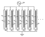
多数の大面積な基板上にアモルファス半導体膜を同時に成膜する場合、平行平板電極対を複数組、並列に配置することにより各基板上に一括して成膜することができる。図4に、従来の平行平板電極対100を複数組並列に並べた場合の装置概略図を示す。隣り合う電極対100、100の隣り合う電極が、カソード電極101同志もしくはアノード電極102同志であっても構わない。アノード電極101にはRF電源104からRF出力が印加され、カソード電極102には基板103がセットされている。なお、基板103はカソード電極102から離れて、電極対100の間に位置するように構成してもよい。また、RF出力は各電極対100…に個別で印加されるように、RF電源を個別で配置してもよい。
【0003】
【発明が解決しようとする課題】
しかしながら、上述した従来の電極101、102の配置では、個々の電極対100…にRF出力を印加して放電すると、お互いの印加電力が干渉し合って、放電は不安定なものになり、各電極対100…の間で発生するプラズマによって形成されるアモルファス半導体膜の成膜速度は大きく異なってしまうという問題があった。
【0004】
この現象は、一つのアノード電極101に対して対をなすカソード電極102ばかりか、隣の電極対100のカソード電極102に対しても平行平板同志であるが故に、放電に干渉がのりやすく、また、電極対100が電極群の中で端に位置するか、中央付近に位置するかでも、干渉の度合いが異なってくるからである。また、個々の電極対100…の干渉の影響を抑えるため、電極対100…の間隔を十分に離した場合、装置全体の容積は拡大し、装置の大型化が余儀なくされてしまうなどの問題があった。
【0005】
この発明は、従来の装置では上述した干渉のため実現不可能であった、大量基板同時形成で、アモルファス半導体膜の高速形成を実現し、スループットを向上させることをその目的としている。
【0006】
【課題を解決するための手段】
この発明の多層薄膜形成装置は、減圧下で平行平板方式のプラズマCVD法を用いて、複数の基板上に同時に膜形成するための電極対を少なくとも3組以上有し、それらの電極対の中間面が実質的に回転対称な放射状に配置された電極対群を含む反応室が複数接続された多層薄膜形成装置であって、上記回転対称となる軸に沿って基板もしくは基板を保持した治具を隣り合った反応室間で移動させる際に、基板もしくは基板を保持した治具を形成時の基板の相対位置が一定に保持できるような固定枠に配置するとともに、隣り合った反応室間のガスが膜形成時に混じり合うことを避けるための空間分離のシール機能を前記固定枠の一部が有することを特徴とする。
【0015】
上記したように構成することで、薄膜形成時の基板の相対位置が一定に保持できるような治具を直線的に移動させるだけ、その移動は特殊な搬送機構を用いる必要がなく、基板の搬送が容易になる。
【0017】
更に、この発明は、隣り合った反応室間のガスが膜形成時に混じり合うことを避けるための空間分離のシール機能を有し、形成時の基板の相対位置が一定に保持できるような固定枠が少なくとも隣り合った反応室間で複数連続して接触していることを特徴とする
【0018】
また、この発明は、少なくとも隣り合った反応室で複数連続して接触しており、形成時の基板の相対位置が一定に保持できるような固定枠の隣り合って接触している部分に、互いにずれないようにするためのほぞを設けるとよい。
【0019】
更に、隣り合った反応室間のガスが膜形成時に混じり合うことを避けるための空間分離のシール機能を有するとともに、少なくとも一方に放射線状に配置された電極対と同程度の大きさのシール材を有する固定枠を備え、この固定枠を隣り合った反応室間で移動させる際に、反応室の移動方向とは異なる側壁に保持された全ての電極が、放射方向に動いて移動のための空間が確保されるように構成すればよい。
【0020】
上記のように構成することで、成膜により発生する反応生成物の剥がれを基板固定枠で毎回回収することができ、メンテナンス頻度をさらに少なくすることができる
【0021】
【発明の実施の形態】
以下、この発明の実施の形態につき図面に基づき説明する。
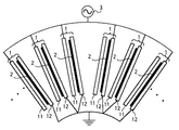
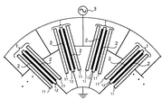
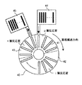
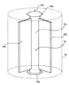
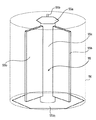
図1は、この発明に用いられる第1のプラズマCVD装置の概略構成を示す要部模式図、図3は平行平板電極対の配置を立体的に示した概略図である。
【0022】
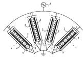
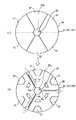
図1に示すように、平行平板電極対1が隣同士互いにほぼ等角度で配置され、すべてのカソード電極11…は、共通の中心軸から放射状に配置される。そして、図1及び図3に示すように、複数組の平行平板電極対1…を放射状に且つ等角度で真空チャンバ4内に配置する。カソード電極11には、RF電源3からRF出力が印加され、アノード電極12には基板2がセットされている。このため、アノード電極12には基板2をセットするための基板ホルダ等が設けられている。
【0023】
尚、基板2はアノード電極12から離れて、平行平板電極対1の間に位置するように構成してもよい。
【0024】
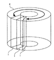
図3は、平行平板電極対1…の配置を立体的に示した概略模式図である。尚、電極対1…の数が増えた場合、電極対1…の外辺の幅(W)と、N組の電極対1で、そのうちの中空円柱(直径>NW/π)形状を有する真空チャンバ4の構造になっている。
【0025】
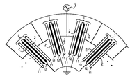
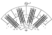
図2は、この発明に用いられる第2のプラズマCVD装置の概略構成を示す要部模式図である。図2に示す平行平板電極1は、一組の平行平板電極1がカソード電極11、アノード電極12、カソード電極11の順に並び、隣同志のカソード電極11が、互いにほぼ等角度で配置され、すべてのカソード電極11…は、共通の中心軸から放射状に配置されている。この図2に示す構造のものにおいてもカソード電極11にはRF電源3からRF出力が印加され、アノード電極12には基板2がセットされている。また、基板2はアノード電極12から離れて、平行平板電極対1の間に位置するように構成してもよい。
【0026】
尚、一組の平行平板電極対1の並びはカソード電極11、アノード電極12、カソード電極11の順で、アノード電極12が放射状に等角度で配置した構造のものでも良い。
【0027】
また、1組の電極対1…の数が増えた場合、電極対…の外辺の幅(W’)と、N組の電極組で、そのうちの中空円柱(直径>NW’/π)形状を有する真空チャンバ4の構造とする。
【0028】
さらに、一組の電極がアノード電極12、カソード電極11、アノード電極12の順に並べた電極群のカソード電極11がメッシュカソードまたはホロカソードであっても良い。
【0029】
上記のように構成した平行平板電極対1…を図3に示すように、中空円柱状の真空チャンバ4に配置することにより、この発明にかかるプラズマCVD装置が形成される。
【0030】
上記したように構成することで、各電極対1…または電極組1…間での放電の干渉が軽減され、各電極対1…または電極組1…で形成される薄膜半導体膜の膜厚の均一化が可能になる。
【0031】
また、カソード電極11を中心に両面がアノード電極12の電極組を使用し、そのカソード電極11がメッシュまたはホロカソードの場合、カソード電極が平板の場合に比べて、同じパワーでも分解効率やガス利用効率が上がり、同じパワーで成膜速度が速くなる。
【0032】
次に、従来の平行平板電極対の並列配置の方法と、この発明における放射状に配置した平行平板電極対の方法にて、アモルファスシリコン膜の形成を行い、各電極対で形成される膜の膜厚を電極対の数と電極対の間隔で比較した結果を示す。
【0033】
従来の装置としては、図4に示すような横方向に複数の電極対100…が配置され、2つの電極101、102との間に基板103が配置され、RF電源104が共有された装置を使用した。この従来の装置の場合、各電極対100…は等間隔ですべて配置されるようにした。アノード電極101、カソード電極102のギャップ間隔は20mmとした。電極対100の外辺の幅はほぼ30cmである。
【0034】
尚、一つの電極は、幅が40cm、縦方向の長さが90cmであり、その電極面積は3600cm2である。また、基板サイズは幅が30cm、縦方向の長さが50cmで、その面積が1500cm2である。基板103はガラス基板またはSnO2基板を使用した。上記したプラズマCVD装置による太陽電池の形成条件を表1に示す。
【0035】
【表1】

各層の形成は、別々の真空チャンバにて行った。アモルファスシリコン膜の形成条件は上記の太陽電池形成条件のi層の形成条件と同じである。
【0037】
基板内の膜厚分布は、基板の中央と端の計5点の膜厚測定時の最大値(以下max)と最小値(以下min)から(膜厚分布)=±(max−min)/(max+min)×100(%)の計算式にて求めた。パワーは各電極間に投入されるパワーが電極対100の数を変えても、ほぼ等しくなるように、各電極間にパワーメータを接続し、電力投入時にこの値がほぼ等しくなるように調整した。
【0038】
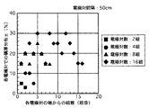
図5に従来の複数基板一括処理装置における電極対の数と各電極対で形成されたアモルファスシリコン膜の膜厚分布を示す。電極対100の数は2、4、8、16組で各々同条件で行い、電極対100の間隔を50cmに固定し、電極対100の数が増えたとき、放電に及ぼす影響を調べた。電極対100の数が最も多い電極対16組の場合、電極対100同志の放電干渉のため、放電が安定せず、形成された膜の膜厚は個々の電極対100で最大±30%の膜厚分布を生じた。電極対100が8組の場合でも、膜厚分布は最大±25%もあった。電極対100が4組の場合で、膜厚分布は最大±10%、電極対2組の場合で、膜厚分布は約±5%になった。膜厚の分布は電極対の数が減るほど向上した。
【0039】
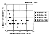
図6に従来の装置の電極対の数と各電極対で形成されたアモルファスシリコン太陽電池特性比較を示す。太陽電池はアモルファスシリコン(a−Si)シングル太陽電池である。サイズは1cm角で、基板サイズ1500cm2以内に等間隔で、10ポイントの変換効率を測定し、その平均値を使用した。10ポイントの測定点のうち、最高効率の80%以下の効率は、平均の算出から除いた。また、歩留まり算出は、平均値の算出に用いたポイント数の測定点総数(10)にしめる割合から求めた。
【0040】
電極対100の数が増えるにつれて、各電極対100での平均変換効率は低下した。尚、歩留まりは電極対数2、4、8、16組で各々90%、70%、60%、40%程度であった。
【0041】
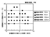
図7に従来の装置の電極対の配置間隔を変えた場合に形成されるアモルファス膜の膜厚分布を示す。電極対100の数は8組で形成条件は統一し、電極対100の間隔を10cm、50cm、100cm、200cmに変えて膜形成を行い、電極対100の間隔の放電に及ぼす影響を調べた。電極対100の間隔が最も狭い10cmの場合、電極対100同志の放電干渉のため、放電が安定せず、形成された膜の膜厚は個々の電極対100で最大±35%の膜厚分布を生じた。電極対100の間隔が100cm、200cmの場合は、膜厚分布は各々最大で±20%と±15%であった。電極の間隔10cmの場合は、膜厚分布は±35%もあり、膜厚の分布は電極対100同志の間隔が狭いほど大きくなった。
【0042】
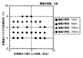
図8は従来の装置の電極対の間隔と各電極対で形成されたアモルファスシリコン太陽電池特性比較を示す。太陽電池はa−Siシングル太陽電池である。
【0043】
電極対100の間隔が狭くなるにつれて平均変換効率は低下した。尚、歩留まりは電極間隔10cm、50cm、100cm、200cmで各々40%、60%、70%、90%程度であった。
【0044】
次に、本発明に用いられるプラズマCVD装置として図1に示すように、2つの電極11、12と基板2が配置され、RF電源3が共有された装置を使用して成膜した場合について説明する。尚、一つの電極は、幅が40cm、縦方向の長さが90cmであり、その電極面積は3600cm2である。また、基板サイズは幅が30cm、縦方向の長さが50cmで、その面積が1500cm2である。基板2としては、ガラス基板を使用した。電極対1の数は12組、18組、36組とした。
【0045】
尚、装置における真空チャンバ4の中空のサイズは直径1.5m、真空チャンバ4の外周の直径は3mである。
【0046】
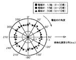
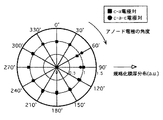
図9に、この発明に用いられるプラズマCVD装置を使用し、電極対1の配置角度Θと各電極対1で形成された膜の規格化膜厚分布を示す。アモルファスシリコン膜の形成は表2の条件に従い行った。
【0047】
【表2】
電極対1が12、18組の場合、各電極対1のなす角度は各々30度と20度になる。両者共に一括して同時形成したアモルファスシリコン膜の個々の電極対1…間での膜厚分布は±5%以下であった。尚、本発明のプラズマCVD装置にてドープ層を形成した場合でも、膜厚分布は±5%以下であり、膜厚分布が低下することはなかった。
【0049】
電極対1が36組の場合、電極対1の角度は10度になる。この場合の膜厚分布は±10%であった。尚、電極数1はこの方法で無限に増やすことは可能であるが、隣り合う電極対1、1間の角度が小さくなるほど、電極11、12は平行に近ずくため、従来の装置の形状と同様の放電干渉の影響が現れる可能性がある。
【0050】
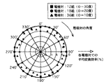
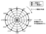
図10にこの発明に用いられるCVD装置を使用し、電極対1の配置角度Θと各電極対で形成された太陽電池の平均変換効率分布を示す。膜形成は上記の表2に示す条件で行った。電極対1が12組、18組、36組すべての場合ともに、歩留まりは100%であった。
【0051】
尚、従来の装置で電極対100が36組、電極対100の間隔が50cmの場合で、電極の占有面積は約18m2に対して、円柱型のこの発明による装置では、占有面積が約13m2であり、省スペース化にもなる。
【0052】
次に、図1に示すアノード電極12とカソード電極11の電極対(以下c−a電極対)が交互にほぼ等角度で配置されたプラズマCVD装置と、図2に示すように、一つのアノード電極12の両面に対向する形で2つのカソード電極11、11が配置された電極組(以下c−a−c電極組)で、各アノード電極12が等角度で放射状に配置されたプラズマCVD装置をそれぞれ用い各装置で成膜した膜の比較を行った。各々のプラズマCVD装置の各アノード電極12間の角度は共に30度とした。RF電源3は共通とした。一つの電極は、幅が40cm、縦方向の長さが90cmであり、その電極面積は3600cm2である。また、基板サイズは幅が30cm、縦方向の長さが50cmで、その面積が1500cm2である。基板2としてはガラス基板またはSnO2基板を使用した。
【0053】
太陽電池の形成条件は表2と同じである。アモルファスシリコン膜の形成条件は太陽電池形成条件のi層形成条件と同じである。
【0054】
基板内膜厚分布は、基板2の中央と端の計5点の膜厚測定時の最大値(以下max)と最小値(以下min)から(膜厚分布)=±(max−min)/(max+min)×100(%)の計算式にて求めた。尚、c−a−c電極組タイプの場合の膜厚分布は、両面合わせた基板内(バッチ内)で求めた。
【0055】
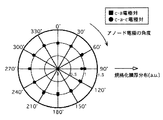
図11に、上記2つのタイプのプラズマCVD装置の各電極対で形成された膜の規格化膜厚分布の比較を示す。c−a電極対タイプの膜厚分布は±5%、c−a−c電極組タイプの膜厚分布は±10%であった。
【0056】
図12に、両者のプラズマCVD装置で形成されたアモルファスシリコン太陽電池の平均変換効率分布の比較を示す、c−a電極対タイプの効率分布は±5%、c−a−c電極組タイプの効率分布は±7%であった。c−a−c電極組タイプは、スループットが約2倍上がった。効率分布は両者でほぼ同じであり、効率分布が±10%以内であれば、量産時の製造コストの低減が可能であった。尚、歩留まりは共に95%以上であった。
【0057】
次に、図13に示す一つの平板カソード電極11の両面に対向する形で2つの平板アノード電極12が配置された電極組1(以下anode−cathode−anode電極組とする)が、等角度で配置されたプラズマCVD装置と、図14に示す一つの平板アノード電極12の両面に対向する形で2つの平板カソード電極11が配置された電極組1(以下、cathode−anode−cathode電極組とする)が、等角度で配置されたプラズマCVD装置にてアモルファスシリコン膜および太陽電池の形成を行った。アモルファスシリコン膜および太陽電池の形成条件は表3に示す。
【0058】
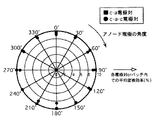
【表3】
図15に示すように、anode−cathode−anode電極組の膜厚分布が±10%に対して、cathode−anode−cathode電極組の膜厚分布は±10%であった。また、図16に示すように、anode−cathode−anode電極組の平均変換効率分布が±8%に対して、cathode−anode−cathode電極組のそれは±8%であった。歩留まりは共に95%以上。両者の電極組の膜厚分布、平均変換効率共に高く、量産に適している。
【0060】
図17に一つのアノード電極12の両面に対向する形で2つのメッシュ型カソード電極11aが配置された電極組(以下mesh−a−meshとする)で、各アノード電極12が等角度で放射状に配置されたプラズマCVD装置の放電部概略図を示す。図18に一つのアノード電極の両面に対向する形で2つのカソード電極が配置された電極組で、各アノード電極が等角度で放射状に配置されたプラズマCVD装置で形成されたアモルファスシリコン膜の規格化膜厚分布のカソード電極が平板型とメッシュ型の比較を示す。図19に一つのアノード電極の両面に対向する形で2つのカソード電極が配置された電極組で、各アノード電極が等角度で放射状に配置されたプラズマCVD装置で形成されたアモルファスシリコン膜のバッチ内平均変換効率分布のカソード電極が平板型とメッシュ型の比較を示す。尚、各々のプラズマCVD装置の各アノード電極対の角度は共に30度とした。RF電源は共通とした。一つの電極は、幅が40cm、縦方向の長さが90cmであり、その電極面積は3600cm2である。また、基板サイズは幅が30cm、縦方向の長さが50cmで、その面積が1500cm2である。基板2としてはガラス基板またはSnO2基板を使用した。太陽電池形成条件を表4に示す。アモルファスシリコン膜の形成条件は太陽電池形成条件のi層形成条件と同じである。
【0061】
【表4】
基板内膜厚分布は、基板の中央と端の計5点の膜厚測定時の最大値(以下max)と最小値(以下min)から(膜厚分布)=±(max−min)/(max+min)×100(%)の計算式にて求めた。尚、膜厚分布および平均変換効率は、アノード電極の両面の基板内(バッチ内)で求めた。
【0063】
平板カソード電極の膜厚分布が±7%に対して、メッシュカソード電極の膜厚分布は±10%であった、また、平板カソード電極の変換効率分布が±7%に対して、メッシュカソード電極の変換効率分布は±10%であった。メッシュカソード電極組タイプは、スループットは、約2倍向上し(表4の成膜速度参照)、効率分布も±10%以内と、良好であった。(効率分布が±10%以内であれば、量産時の製造コストの低減が可能であった。)歩留まりは共に95%以上であった。
【0064】
尚、平板カソード電極で成膜速度をメッシュカソードと同程度にした場合は、効率分布は±15%以上となってしまい、量産に適さなかった。
【0065】
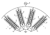
次に、図20に示すように、一つのメッシュカソード電極11aの両面に対向する形で2つのアノード電極12、12が配置された電極組1(以下anode−mesh−anode電極組とする)が、等角度で配置されたプラズマCVD装置にてアモルファスシリコン膜および太陽電池の形成を行った。膜および太陽電池の形成条件は表4(括弧内の値)に同じである。
【0066】
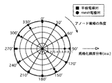
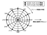
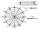
図21に示すように、mesh−anode−mesh電極組の膜厚分布が±10%に対して、anode−mesh−anode電極組の膜厚分布は±5%であった。また、図22に示すように、mesh−anode−mesh電極組の平均変換効率分布が±10%に対して、anode−mesh−anode電極組のそれは±5%であった。歩留まりは共に95%以上。anode−mesh−anode電極組の方が、mesh−anode−mesh電極組のより膜厚分布、平均変換効率共に高く、量産に適している。
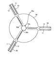
【0067】
図23に一つのホロカソード電極11bの両面に対向する形で2つの平板型アノード電極12、12と基板2が配置された電極対1(以下anode−hollow cathode−anodeとする)で、各ホロカソード電極11bが等角度で放射状に配置されたプラズマCVD装置の放電部の概略図を示す。図24に本発明のプラズマCVD装置で形成されたアモルファスシリコン膜の規格化膜厚分布のカソード電極がホロカソード電極11bとメッシュカソード電極11aの比較を示す。メッシュカソード電極11aの膜厚分布が±10%に対して、ホロカソード電極11bの膜厚分布は±8%であった。
【0068】
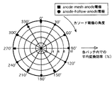
図25に本発明に用いられるプラズマCVD装置で形成されたアモルファスシリコン太陽電池の平均変換効率分布のカソード電極がホロカソード電極11bとメッシュカソード電極11aの比較を示す。メッシュカソード電極11aの効率分布が±5%に対して、ホロカソード電極の効率分布も±4%であった。歩留まりは共に95%以上。反応条件は表4()内の条件に同じである。
【0069】
ホロカソード電極11bの方がメッシュカソード電極11aに比べて、プラズマ閉じこめ効果があり、ガス分解が促進されると共に、成膜表面のイオン衝撃の低減が可能である。その結果として効率の絶対値や効率分布も若干、ホロカソード電極11bの方が良かった。
【0070】
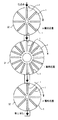
図26は、上記したこの発明に用いられるCVD装置を用いて、アモルファスシリコン太陽電池を連続形成する多層薄膜形成装置の第1の参考例を示す模式図である。
【0071】
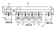
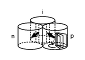
各反応室20、21、22はそれぞれ上記したように、平行平板方式で、プラズマを生成するためのカソード電極とアノード電極からなる電極対が3つ以上含まれる電極群から構成され、各電極対の中間面が実質的に放射状に配置されている。各反応室20、21、22は搬送室24を介して接続されている。反応室20では基板上にp型アモルファスシリコン膜が形成され、p型アモルファスシリコン膜が形成された基板が多数基板ホルダー23により、反応室20から搬送室24に取り出される。そして、反応室21の各電極間に基板ホルダー23から基板がセットされる。この反応室21でi型アモルファスシリコン膜が形成される。そして、i型アモルファスシリコン膜が形成された基板が多数基板ホルダー23により、反応室21から搬送室24に取り出される。そして、反応室22の各電極間に基板ホルダー23から基板がセットされる。この反応室22でn型アモルファスシリコン膜が形成される。なお、搬送室24内においては、基板は、放射状に配置されて成膜される時の状態で搬送される。
【0072】
通常、p型、n型アモルファスシリコン膜よりi型アモルファスシリコン膜は厚く形成されるので、p型、n型アモルファスシリコン膜の形成時間よりi型アモルファスシリコン膜の形成時間が長くなる。そこで、i型の反応室21を複数に増やして、pからi、iからnへの搬送待ち時間を少なくしている。例えば、p型、n型アモルファスシリコン膜の形成時間が5分間、i型アモルファスシリコン膜の形成時間が20分とすると、i型の反応室21を4つにし、搬送待ち時間を無くすように構成している。
【0073】
図27は、上記したこの発明に用いられるCVD装置を用いて、アモルファスシリコン太陽電池を連続形成する多層薄膜形成装置の第2の参考例を示す模式図である。
【0074】
各反応室30、31、32はそれぞれ上記したように、平行平板方式で、プラズマを生成するためのカソード電極とアノード電極からなる電極対1が3つ以上含まれる電極群から構成され、各電極対1の中間面が実質的に放射状に配置されている。各反応室30、31、32はゲートバルブを介して接続されている。各反応室30、31、32内での各アモルファスシリコン膜の成膜は、電極対毎反応室内で回転しながら行われる。反応室30のaから基板が搬入され、この反応室内30でp型アモルファスシリコン膜がbまでの回転する間に形成される。例えば、p型アモルファスシリコン膜の形成時間が5分間の場合には、aからbに至るまで5分間で回転するように構成されている。そして、b地点まで基板が搬送されるとゲートバルブから反応室31のcを経て反応室31内に基板が搬入される。
【0075】
この反応室内31でi型アモルファスシリコン膜がdまで回転する間に形成される。例えば、i型アモルファスシリコン膜の形成時間が10分間の場合には、cからdに至るまで10分間で回転するように構成されている。そして、d地点まで基板が搬送されるとゲートバルブから反応室32のeを経て反応室32内に基板が搬入される。
【0076】
この反応室内32でn型アモルファスシリコン膜がfまでの回転する間に形成される。例えば、n型アモルファスシリコン膜の形成時間が5分間の場合には、cからdに至るまで5分間で回転するように構成されている。そして、f地点まで基板が搬送されるとゲートバルブからfを経て基板が取り出される。
【0077】
なお、上記した装置においては、各反応室の左半分の電極対間には基板がない状態で回転することになる。
【0078】
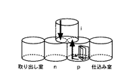
図28は、上記したこの発明に用いられるCVD装置を用いて、アモルファスシリコン太陽電池を連続形成する多層薄膜形成装置の第3の参考例を示す模式図である。この装置は真空チャンバ40の中がp型反応室41、i型反応室42、n型反応室43の3室に大きく分離され、各反応室間はシャワーカーテン等で分離されている。各電極対は真空チャンバ40の中を円周方向に成膜されながら一定の搬送速度で移動する。
【0079】
例えば、p型、n型アモルファスシリコン膜の成膜時間が5分、i型アモルファスシリコン膜の成膜時間が10分の場合は、p型反応室41、i型反応室42、n型反応室43の中心角度をそれぞれ90°、180°、90°に分離して、仕込室44から基板をp型反応室41に搬入し、成膜しながらn型反応室43の端の取り出し室45に向かって電極対が等速度で回転し、成膜が終わった基板が取り出し室45に送り出される。
【0080】
なお、反応室の分離はシャワーカーテン等で行い各反応室の反応圧力は等しくする。
【0081】
上記したアモルファスシリコン太陽電池を連続形成する多層薄膜形成装置においては、基板の搬送方法が従来の多層膜生成装置に比べて複雑若しくは大型化する。例えば、第1の参考例では、反応室とは別に搬送室などの特別の搬送機構を設けているので、装置が大型化する。また、第2、第3の参考例では、基板を回転させる必要があり、基板の搬送方法が複雑となる。更に、基板ヒーターを内蔵した電極ごと基板を搬送する必要があり、装置が複雑になることは否めない。
【0082】
そこで、上記したこの発明に用いられるCVD装置を用い、搬送機構を簡略化したアモルファスシリコン太陽電池を連続形成する多層薄膜形成装置の第1の実施の形態につき説明する。
【0083】
この第1の実施の形態の基本構成は、図29に示すように、この発明にかかるプラズマCVD装置を縦又は横方向に一列に配置し、基板のみ保持する基板ホルダー保持部を有する基板ホルダー保持固定枠のみを電極対1…の回転対称となる軸に沿って移動させるように構成する。基板ホルダーに保持された基板のみを各反応室に移動させるものである。
【0084】
図29に示すように、仕込室50からp型アモルファスシリコン膜を形成する第1反応室51、i型アモルファスシリコン膜を形成する第2反応室52、n型アモルファスシリコン膜を形成する第3反応室53と、取り出し室54が縦又は横方向に一列に連接して設けられている。連接された仕込室50、反応室51…、取り出し室54間を基板ホルダー保持固定枠が電極対1…の回転対称となる軸に沿って移動する。この移動は直線移動のため、搬送機構は簡単な構成で実現できる。
【0085】
また、移動仕込室50と取り出し室54の両側はゲートバルブ構造とし、真空−大気圧間の圧力差に耐えられるように構成され、他の反応室51…間は簡単なシール機構のみで分離している。
【0086】
通常、p型、n型アモルファスシリコン膜よりi型アモルファスシリコン膜は厚く形成されるので、p型、n型アモルファスシリコン膜の形成時間よりi型アモルファスシリコン膜の形成時間が長くなる。i型の反応室51の軸方向の長さを長くして複数の固定枠55が挿入されるように構成して、pからi、iからnへの搬送待ち時間を少なくしてもよい。
【0087】
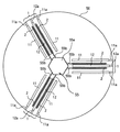
図30は、この第1の実施の形態における各反応室を上部から見た状態を示す平面図、図31は、一つの反応室内における基板ホルダー保持固定枠の斜視図である
【0088】
図30及び図31に従い上記したこの発明に用いられるプラズマCVD装置を用いた多層薄膜形成装置の第1の実施の形態につき更に説明する。
【0089】
平行平板方式でプラズマを生成するためのカソード電極11及びアノード電極12からなる電極対1…は反応室内に3組設けている。そして、一つの電極は、前述したように、幅が40cm、縦方向の長さが90cmである。また、カソード電極11とアノード電極12間の電極の間隔は2cmとした。これら3つの電極対1…は、電極対の中間面が実質的に回転対称な放射状になるように、反応室壁56にカソード電極保持部11a及びアノード電極保持部12aを介して両電極11、12が取り付けられている。
【0090】
この実施の形態では、反応室51…の中央部に上記電極対1…の回転対称となる軸に沿って移動可能な基板ホルダー保持固定枠55が配置される。この固定枠55は、固定枠軸部55cに前記電極対1…の中間部に基板1を保持可能な基板ホルダー保持部55bが放射状に取り付けられている。
【0091】
前述したように、基板2は幅が30cm、縦方向の長さが50cmのガラス基板が用いられ、この基板2が金属製の基板ホルダー(図示せず)にはめ込まれ、固定される。基板2を取り付けた基板ホルダーを薄膜形成時の基板の相対位置が一定に保持できるように、基板ホルダー保持部55bに取り付ける。固定枠55の基板ホルダー保持部55bに設置された基板2は、固定枠55を反応室51内の所定の位置に移動すると、電極対1の間に一定に保持される。この基板ホルダー保持部55bに基板1を保持した状態で、原料ガスをプラズマ分解し、基板2上に薄膜を堆積させる。
【0092】
ここで、基板ホルダー保持部55bは熱容量を下げるために、十分な強度をもった枠だけのフレーム構造としている。
【0093】
前述した第1ないし第3の参考例に示されている多層薄膜形成装置が、各反応室間をゲートバルブで隔離し、移動形態から基板やヒータ内蔵の基板ホルダーの移送を各反応室内に設けたロボットアームなどの搬送機構により行う必要がある。
【0094】
これに対して、この第1の実施の形態においては、形成時の基板の相対位置が一定に保持できるような固定枠55を直線的に移動させるだけ、その移動は特殊な搬送機構を用いる必要がない。
【0095】
また、基本的に各反応室51…には、一方の基板ホルダー保持固定枠の上接触部55aと他方の基板ホルダー保持固定枠の下接触部55dを接触させた状態で固定枠55が設置される。そして、反応室内の固定枠55を同時に次の反応室に移動させることで、各反応室内には特別な搬送機構を設けていない。ただし、固定枠55がずれないように、各反応室51内にガイドを設けてもよい。このようなガイドを設けても膜形成には影響しない。
【0096】
また、この実施の形態においては、基板ホルダー保持具固定枠の上接触部55aに凸構造を、基板ホルダー保持固定枠の下接触部55dに凹構造を設けてほぞとし、互いの固定枠55…がずれないように構成している。
【0097】
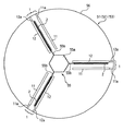
薄膜形成時の基板2の相対位置が一定に保持できるような固定枠55の基板ホルダー保持固定枠の上接触部55aや基板ホルダー保持固定枠の下接触部55dが、各反応室(真空チャンバ)空間を分離する様子を図32に示す。図32(a)は膜形成時の真空チャンバを分離している状態、同(b)は固定枠55の移動状態を示す状態をそれぞれ示す平面図である。
【0098】
真空チャンバ空間シール用分離板部57は、反応室壁56に放射方向に移動可能に取り付けられており、反応時と、固定枠55が移動するときにそれぞれ図32(a)の状態と(b)の状態になるように移動する。
【0099】
図32(a)に示すように、膜形成時には、空間を分離する空間シール用分離板部57と、基板ホルダー保持固定枠の上接触部55aまたは下接触部55dとが接触する。このように、真空チャンバ空間シール用分離板57と、両接触部55a、55dが接触することで、反応室51…の間でガスの混合が防止される。
【0100】
また、固定枠55の移送時には、空間を分離する空間シール用分離板部57が放射方向に移動することで、固定枠55が移動するための空間が広がる。このとき、原料ガスの混合をより抑制するために、基板ホルダー保持固定枠の上接触部55a及び基板ホルダー保持固定枠の下接触部55dの両方が空間分離を行っていてもよい。更に、i型層を形成する反応室52の圧力を他の反応室51、53の圧力より高くすることで、i型層を形成する反応室52内に不純物ドーパントガスが混入するのを確実に防止できる。
【0101】
また、原料ガスの混合を抑制する方法として、空間を分離する真空チャンバ空間シール用分離板部57の一部に穴を設けて、基板ホルダー保持固定枠の上接触部55aと基板ホルダー保持固定枠の下接触部55dの間からガス排気をするような方法を用いてもよい。
【0102】
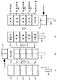
次に、この第1の実施の形態における基板の搬送手順、即ち、基板ホルダー保持固定枠55の搬送手順を図33に従い説明する。
【0103】
図33(a)に示すように、搬送機構58を取り出し室54の下方部から取り出し室方向54に向かって移動させ、反応室51、52、53を所定の圧力に真空引きし、また、取り出し室54も真空引きする。仕込室50と反応室51との間のゲートバルブは閉鎖しておき、仕込室50は大気状態のままにしておく。
【0104】
続いて、図33(b)に示すように、仕込室50の上に基板2を基板ホルダー保持部55bに設置した固定枠55を置く。この状態で、各反応室51…に基板がある場合には、プラズマ分解により基板2上に薄膜が形成されている。
【0105】
図33(c)に示すように、仕込室50を真空引きし、所定の真空度になった状態で、仕込室50の反応室側ゲートバルブを開放し、固定枠55を軸方向に沿って、移動させる。この移動により、それぞれの反応室の固定枠は次の反応室に移動する。取り出し室54に成膜が終了した基板を保持した固定枠55が移動すると、取り出し室54の反応室側のゲートバルブを閉鎖し、取り出し室54を大気状態にする。
【0106】
図33(d)に示すように、成膜が終了した基板を保持した固定枠55を取りだした後、取り出し室54のゲートバルブを閉鎖し、取り出し室54を真空引きする。この時、仕込室50内は加熱され、基板を所定温度に加熱している。
【0107】
上記した各工程を簡単に纏めると以下の通りになる。
【0108】
(1)仕込室50の上に基板2を設置した固定枠55を置く。
(2)仕込室50を大気状態にして固定枠55を仕込室50に導入する。
(3)仕込室50を真空引きする。
(4)基板2を加熱する
(5)p、i、n各反応室51、52、53にて膜形成を行う。
(6)固定枠55を取り出し室54に移送する。
(7)基板2を冷却後、取り出し室54を大気状態にして固定枠55を取り出す。
【0109】
(1)〜(4)と(5)及び(7)は平行して行うプロセスである。各反応室間を移送するとき、固定枠55は仕込室50、第1反応室(p室)51、第2反応室(i室)52、第3反応室(n室)53内にあり、これらを全て同時に次の反応室(真空チャンバ)へ移送させている。この移送は取り出し室54内に設けた搬送機構のみにより行っている。また、仕込室50内への移送は仕込室50内の搬送機構により、取り出し室54からの取り出しは装置下部に設けた搬送機構58により行っている。
【0110】
このように各反応室51…内には特別な搬送機構を設けておらず、放電に影響するようなものが反応室51…内に無いために、反応室51…内に余分な空間を設ける必要がなく、形成される膜の均一性も向上する。
【0111】
上記したように、仕込室50および取り出し室54の両側はゲートバルブ構造とし、真空−大気間の圧力差に耐えられるようにしているが、他の反応室間は簡単なシール機構のみで分離している。
【0112】
本発明装置を用いて形成した光起電力素子の代表的な形成条件を表5に示す。 尚、反応室は、p層、バッファ(b)層、i層、n層の4つの反応室に仕込み室と取り出し室を設けた多層薄膜形成装置を用いた。
【0113】
【表5】
それぞれの反応室において形成した膜や、結果として得られた光起電力素子の特性の均一性は、前述した実施の記値と同様に±5%と特に差はなかったが、搬送が容易になることでタクトタイムが70分から49分と30%削減できた。
【0115】
さらに、反応室内に搬送機構がなく、反応生成物が剥がれて起こる特性歩留まりも抑制でき、結果としてメンテナンス頻度を週1回から月1回に減らすことによる稼働率の向上が実現できた。
【0116】
反応室間は簡単なシール機構のみで分離しているだけであるが、セル特性に特に低下はみられなくなった。しかし、反応室間の圧力差が大きくなった場合にはガス混入が生じやすくなるため、隣接する反応室間の圧力差は大きくならない方がよい。
【0117】
図34に第1の実施の形態における多層薄膜形成装置において、1つの反応室に図2に示すプラズマCVD装置を用いた実施の形態の上面図を示す。一つのアソード電極12を挟んで、基板2及び基板ホルダー保持部55bとカソード電極11が2組あることで、生産性が2倍になる。この場合も、搬送機構に関しては上記した実施の形態と特に変わるところはない。形成した光起電力素子の特性も同一ロットでは±5%の範囲で良好であった。
【0118】
図35に第1の実施の形態における一反応室内における基板搬送用の固定枠55の他の例の斜視図を示す。
【0119】
この固定枠55は基板ホルダー保持固定枠の下接触部55d1を基板ホルダー保持部55bの外辺部の領域まで拡げているところが前述の実施の形態と異なる。これにより、成膜により発生する反応生成物の剥がれを基板ホルダー保持固定枠55で毎回回収することができ、メンテナンス頻度をさらに少なくすることができる。実際、メンテナンス頻度を月2回にすることができた。
【0120】
但し、このとき搬送時に基板ホルダー保持固定枠の下接触部55d1が通るスペースを確保するために、図36に示すように放電電極1…を放射状に外側へ移動可能なように収容部59を設け、放電電極1…を放射状に外側へ移動させる構造にしている。
【0121】
以上、述べたように、この発明のプラズマCVD法を用いた反応室が複数接続された多層薄膜形成装置において、上記回転対称となる軸に沿って基板ホルダー保持固定枠を隣り合った反応室間で移動させる際に、基板もしくは基板を保持したホルダーを形成時の基板の相対位置が一定に保持できるような固定枠に配置したものを一つの形成単位とし、複数の基板の相対位置を厳密に保ったまま、簡単な搬送機構を導入できるために、プロセスの量産性及び信頼性が高められる。
【0122】
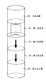
図37は、上記したこの発明に用いられるCVD装置を用いて、アモルファスシリコン太陽電池を連続形成する多層薄膜形成装置の第4の参考例を示す模式図である。この図37に示す装置は、上記したこの発明に用いられるp,n用のプラズマCVD装置上にi用プラズマCVD装置を配置し、基板を上下に1枚ずつ搬送するように構成している。
【0123】
図38は、上記したこの発明に用いられるCVD装置を用いて、アモルファスシリコン太陽電池を連続形成する多層薄膜形成装置の第5の参考例を示す模式図である。この図31に示す装置は、上記したこの発明に用いられるp、i、nのそれれぞれのプラズマCVD装置を各反応室の側面が互いに接するように配置し、接する面にゲートバルブを設けて基板を搬送するように構成している。
【0124】
【発明の効果】
以上説明したように、この発明によれば、大面積且つ大量の基板上に薄膜太陽電池を製造した場合、各電極対間で得られる個々の大面積太陽電池特性の均一化が向上すると共に、歩留まりを向上させることができる。
【0125】
また、カソード電極がホロカソードまたはメッシュカソードとすることで、太陽電池製造のスループットを約1.5〜2倍向上させることができる。
【図面の簡単な説明】
【図1】 この発明に用いられる第1のプラズマCVD装置の概略構成を示す要部模式図である。
【図2】 この発明に用いられる第2の実施の形態にかかるプラズマCVD装置の概略構成を示す要部模式図である。
【図3】 この発明に用いられるプラズマCVD装置における平行平板電極対の配置を立体的に示した概略図である。
【図4】 従来の複数基板を一括処理するプラズマCVD装置の概略構成を示す要部模式図である。
【図5】 従来の複数基板を一括処理するプラズマCVD装置における各電極対で形成されたアモルファスシリコン膜の膜厚分布の電極対の数依存性を示す図である。
【図6】 従来の複数基板を一括処理するプラズマCVD装置における各電極対で形成されたアモルファスシリコン太陽電池の基板内の平均変換効率の電極対の数依存性を示す図である。
【図7】 従来の複数基板を一括処理するプラズマCVD装置における各電極対で形成されたアモルファスシリコン膜の膜厚分布の電極対の間隔依存性を示す図である。
【図8】 従来の複数基板を一括処理するプラズマCVD装置における各電極対で形成されたアモルファスシリコン太陽電池の基板内の平均変換効率の電極対の間隔依存性を示す図である。
【図9】 この発明に用いられるプラズマCVD装置における各電極対で形成されたアモルファスシリコン太陽電池の規格化膜厚分布の電極対間の角度依存性を示す図である。
【図10】 この発明に用いられるプラズマCVD装置における各電極対で形成されたアモルファスシリコン太陽電池の基板内の平均変換効率の電極対の数依存性を示す図である。
【図11】 この発明に用いられるプラズマCVD装置におけるアノード−カソード電極対タイプとカソード−アノード−カソード電極タイプの各電極対でそれぞれ形成されたアモルファスシリコン膜の規格化膜厚分布の電極対間の角度依存性を示す図である。
【図12】 この発明に用いられるプラズマCVD装置におけるアノード−カソード電極対タイプとカソード−アノード−カソード電極タイプの各電極対でそれぞれ形成されたアモルファスシリコン太陽電池の基板内の平均変換効率の電極対間の角度依存性を示す図である。
【図13】 この発明に用いられる他のプラズマCVD装置の概略構成を示す要部模式図である。
【図14】 この発明に用いられる更に異なるプラズマCVD装置の概略構成を示す要部模式図である。
【図15】 この発明に用いられるプラズマCVD装置におけるアノード−カソード−アノード電極対タイプとカソード−アノード−カソード電極タイプの各電極対でそれぞれ形成されたアモルファスシリコン膜の規格化膜厚分布の電極対間の角度依存性を示す図である。
【図16】 この発明に用いられるプラズマCVD装置におけるアノード−アノード−カソード電極対タイプとカソード−アノード−カソード電極タイプの各電極対でそれぞれ形成されたアモルファスシリコン太陽電池の基板内の平均変換効率の電極対間の角度依存性を示す図である。
【図17】 この発明に用いられるカソード電極にメッシュカソード電極を用いたプラズマCVD装置の概略構成を示す要部模式図である。
【図18】 この発明に用いられるプラズマCVD装置におけるカソード−アノード−カソード電極タイプの各電極対において、平板カソード電極とメッシュカソード電極でそれぞれ形成されたアモルファスシリコン膜の規格化膜厚分布の電極対間の角度依存性を示す図である。
【図19】 この発明に用いられるプラズマCVD装置におけるカソード−アノード−カソード電極タイプの各電極対において、平板カソード電極とメッシュカソード電極でそれぞれ形成されたアモルファスシリコン太陽電池の基板内の平均変換効率の電極対間の角度依存性を示す図である。
【図20】 この発明に用いられるカソード電極にメッシュカソード電極を用いたプラズマCVD装置の概略構成を示す要部模式図である。
【図21】 この発明に用いられるプラズマCVD装置におけるメッシュ型カソード電極タイプの各電極対において、アノード−メッシュ型カソード−アノード電極対とメッシュ型カソード−アノード電極−メッシュ型カソード電極対でそれぞれ形成されたアモルファスシリコン膜の規格化膜厚分布の電極対間の角度依存性を示す図である。
【図22】 この発明に用いられるプラズマCVD装置におけるメッシュ型カソード電極タイプの各電極対において、アノード−メッシュ型カソード−アノード電極対とメッシュ型カソード−アノード電極−メッシュ型カソード電極対でそれぞれ形成されたアモルファスシリコン太陽電池の基板内の平均変換効率の電極対間の角度依存性を示す図である。
【図23】 この発明に用いられるカソード電極にホロカソード電極を用いたプラズマCVD装置の概略構成を示す要部模式図である。
【図24】 この発明に用いられるプラズマCVD装置におけるホロ型カソード電極タイプの各電極対において、アノード−メッシュ型カソード−アノード電極対とアノード−ホロカソード−アノード電極対でそれぞれ形成されたアモルファスシリコン膜の規格化膜厚分布の電極対間の角度依存性を示す図である。
【図25】 この発明に用いられるプラズマCVD装置におけるホロ型カソード電極タイプの各電極対において、アノード−メッシュ型カソード−アノード電極対とアノード−ホロカソード−アノード電極対でそれぞれ形成されたアモルファスシリコン太陽電池の基板内の平均変換効率の電極対間の角度依存性を示す図である。
【図26】 この発明に用いられるCVD装置を用いてアモルファスシリコン太陽電池を連続形成する多層薄膜形成装置の第1の参考例を示す模式図である。
【図27】 この発明に用いられるCVD装置を用いてアモルファスシリコン太陽電池を連続形成する多層薄膜形成装置の第2の参考例を示す模式図である。
【図28】 この発明に用いられるCVD装置を用いてアモルファスシリコン太陽電池を連続形成する多層薄膜形成装置の第3の参考例を示す模式図である。
【図29】 この発明に用いられるCVD装置を用いてアモルファスシリコン太陽電池を連続形成する多層薄膜形成装置の第1の実施の形態を示す模式図である。
【図30】 この第1の実施の形態における各反応室を上部から見た状態を示す平面図である。
【図31】 一つの反応室内における基板ホルダー保持固定枠の斜視図である
【図32】 反応室間の空間分離シール部の動作概念を示す平面図である。
【図33】 第1の実施の形態における基板の搬送手順を示す模式図である。
【図34】 第1の実施の形態における多層薄膜形成装置において、1つの反応室に図2に示すプラズマCVD装置を用いた形態を示す上面図である。
【図35】 第1の実施の形態における一反応室内における基板搬送用の固定枠の他の例の斜視図である。
【図36】 図35に示す固定枠を用いた場合の反応室の形状を示す模式図である。
【図37】 この発明に用いられるCVD装置を用いてアモルファスシリコン太陽電池を連続形成する装置の第4の参考例を示す模式図である。
【図38】 この発明に用いられるCVD装置を用いてアモルファスシリコン太陽電池を連続形成する装置の第5の参考例を示す模式図である。
【符号の説明】
1 電極対
11 カソード電極
12 アノード電極
2 基板
3 RF電源[0001]
BACKGROUND OF THE INVENTION
The present invention relates to a plasma CVD apparatus. Multi-layer thin film forming equipment using Especially suitable for forming solar cells collectively on multiple large-area substrates for large area production and mass production of thin film solar cells Equipment It is about.
[0002]
[Prior art]
In the case where an amorphous semiconductor film is simultaneously formed on a large number of large-area substrates, a plurality of pairs of parallel plate electrodes can be formed in parallel by forming a plurality of parallel plate electrode pairs in parallel. FIG. 4 is a schematic view of an apparatus when a plurality of conventional parallel
[0003]
[Problems to be solved by the invention]
However, in the arrangement of the
[0004]
This phenomenon is not only caused by the
[0005]
An object of the present invention is to realize high-speed formation of an amorphous semiconductor film and improve throughput by simultaneous formation of a large number of substrates, which cannot be realized by the above-described interference in a conventional apparatus.
[0006]
[Means for Solving the Problems]
The multilayer thin film forming apparatus of the present invention is Decrease At least three electrode pairs for forming films simultaneously on a plurality of substrates using a parallel plate type plasma CVD method under pressure, and the intermediate surfaces of these electrode pairs are radially rotationally symmetric. A multilayer thin film forming apparatus in which a plurality of reaction chambers including a group of electrode pairs arranged are connected, and the substrate or a jig holding the substrate is moved between adjacent reaction chambers along the rotationally symmetric axis. Hold the board or the board Tajiki The tool is placed on a fixed frame so that the relative position of the substrate during formation can be held constant. In addition, a part of the fixed frame has a space separating seal function for preventing gas between adjacent reaction chambers from being mixed during film formation. .
[0015]
By configuring as described above, the relative position of the substrate during thin film formation can be kept constant. Naji As long as the tool is moved linearly, it is not necessary to use a special transport mechanism, and the transport of the substrate becomes easy.
[0017]
Furthermore, the present invention provides a fixed frame that has a sealing function of space separation for avoiding gas mixing between adjacent reaction chambers during film formation, and that can keep the relative position of the substrate constant during formation. Are in contact with each other between at least two adjacent reaction chambers.
[0018]
In addition, the present invention provides a plurality of continuous contact in at least adjacent reaction chambers, and the adjacent contact portions of the fixed frame that can hold the relative position of the substrate at the time of formation constant to each other. It is good to provide a tenon to prevent it from shifting.
[0019]
Furthermore, it has a sealing function of space separation for preventing gas between adjacent reaction chambers from being mixed at the time of film formation, and at the same time, a sealing material having the same size as a pair of electrodes radially arranged on at least one side Fixed frame with Equipped with this fixed frame When moving between adjacent reaction chambers, all the electrodes held on the side walls different from the moving direction of the reaction chambers may move in the radial direction to secure a space for movement. .
[0020]
By configuring as described above, the peeling of the reaction product generated by the film formation can be collected every time with the substrate fixing frame, and the maintenance frequency can be further reduced.
[0021]
DETAILED DESCRIPTION OF THE INVENTION
Hereinafter, embodiments of the present invention will be described with reference to the drawings.
FIG. 1 shows the present invention. The first program used for The principal part schematic diagram which shows schematic structure of a plasma CVD apparatus, FIG. 3 is the schematic which showed the arrangement | positioning of a parallel plate electrode pair in three dimensions.
[0022]
As shown in FIG. 1, parallel
[0023]
The
[0024]
FIG. 3 is a schematic diagram schematically showing the arrangement of the parallel
[0025]
FIG. 2 shows the present invention. The second process used for It is a principal part schematic diagram which shows schematic structure of a plasma CVD apparatus. The
[0026]
The pair of parallel plate electrode pairs 1 may be arranged in the order of the
[0027]
Further, when the number of electrode pairs 1 increases, the width (W ′) of the outer sides of the electrode pairs, and N electrode groups, of which a hollow cylinder (diameter> NW ′ / π) shape The structure of the
[0028]
Further, the
[0029]
As shown in FIG. 3, the parallel plate electrode pairs 1... Configured as described above are arranged in a hollow
[0030]
By configuring as described above, discharge interference between each
[0031]
In addition, when an electrode set having both surfaces of the
[0032]
Next, an amorphous silicon film is formed by the conventional parallel plate electrode pairing method and the radially parallel parallel plate electrode pair method of the present invention. The result of having compared thickness by the number of electrode pairs and the space | interval of an electrode pair is shown.
[0033]
As a conventional apparatus, a plurality of electrode pairs 100 are arranged in the lateral direction as shown in FIG. 4, a
[0034]
One electrode has a width of 40 cm and a longitudinal length of 90 cm, and its electrode area is 3600 cm. 2 It is. The substrate size is 30 cm wide, 50 cm long in the vertical direction, and its area is 1500 cm. 2 It is. The
[0035]
[Table 1]
Each layer was formed in a separate vacuum chamber. The formation conditions of the amorphous silicon film are the same as the formation conditions of the i layer in the above solar cell formation conditions.
[0037]
The film thickness distribution in the substrate is (film thickness distribution) = ± (max−min) / from the maximum value (hereinafter referred to as max) and the minimum value (hereinafter referred to as min) when measuring the film thickness at a total of five points at the center and end of the substrate. It calculated | required with the formula of (max + min) x100 (%). A power meter was connected between each electrode so that the power supplied between each electrode was substantially equal even when the number of electrode pairs 100 was changed, and this value was adjusted to be approximately equal when the power was turned on. .
[0038]
FIG. 5 shows the number of electrode pairs and the thickness distribution of the amorphous silicon film formed by each electrode pair in a conventional multiple substrate batch processing apparatus. The number of electrode pairs 100 was 2, 4, 8, and 16 under the same conditions. The distance between the electrode pairs 100 was fixed to 50 cm, and when the number of electrode pairs 100 increased, the influence on discharge was examined. In the case of 16 electrode pairs having the largest number of electrode pairs 100, the discharge is not stable due to discharge interference between the electrode pairs 100, and the film thickness of the formed film is maximum ± 30% for each
[0039]
FIG. 6 shows a comparison of the number of electrode pairs of a conventional device and the characteristics of amorphous silicon solar cells formed by each electrode pair. The solar cell is an amorphous silicon (a-Si) single solar cell. The size is 1cm square and the board size is 1500cm. 2 The conversion efficiency of 10 points was measured at regular intervals within and the average value was used. Of the 10 measurement points, an efficiency of 80% or less of the maximum efficiency was excluded from the average calculation. Yield calculation was obtained from the ratio of the total number of measurement points (10) used for calculating the average value.
[0040]
As the number of electrode pairs 100 increased, the average conversion efficiency in each
[0041]
FIG. 7 shows the film thickness distribution of the amorphous film formed when the arrangement interval of the electrode pair of the conventional apparatus is changed. The number of electrode pairs 100 was eight, and the formation conditions were unified. Film formation was performed by changing the distance between the electrode pairs 100 to 10 cm, 50 cm, 100 cm, and 200 cm, and the influence of the distance between the electrode pairs 100 on the discharge was examined. When the distance between the electrode pairs 100 is 10 cm, the discharge is not stable due to discharge interference between the electrode pairs 100, and the film thickness of the formed film is a maximum thickness distribution of ± 35% in each
[0042]
FIG. 8 shows a comparison between the electrode pair intervals of the conventional device and the characteristics of the amorphous silicon solar cell formed by each electrode pair. The solar cell is an a-Si single solar cell.
[0043]
The average conversion efficiency decreased as the distance between the
[0044]
Next, the present invention Used in As shown in FIG. 1 as a plasma CVD apparatus, two
[0045]
The hollow size of the
[0046]
FIG. 9 shows the present invention. Used in The arrangement | positioning angle (theta) of the
[0047]
[Table 2]
When there are 12 and 18 electrode pairs 1, the angles formed by each
[0049]
When the number of electrode pairs 1 is 36, the angle of the
[0050]
FIG. 10 shows the present invention. C used for The arrangement | positioning angle (theta) of the
[0051]
In addition, when the
[0052]
Next, a plasma CVD apparatus in which electrode pairs of the
[0053]
The conditions for forming the solar cell are the same as in Table 2. The formation conditions of the amorphous silicon film are the same as the i layer formation conditions of the solar cell formation conditions.
[0054]
The film thickness distribution in the substrate is calculated from the maximum value (hereinafter referred to as max) and the minimum value (hereinafter referred to as min) at the time of film thickness measurement at a total of five points at the center and end of the substrate 2 (film thickness distribution) = ± (max−min) / It calculated | required with the formula of (max + min) x100 (%). In addition, the film thickness distribution in the case of the c-a-c electrode assembly type was determined in the substrate (in batch) in which both surfaces were combined.
[0055]
FIG. 11 shows a comparison of the normalized film thickness distributions of the films formed by the respective electrode pairs of the above two types of plasma CVD apparatuses. The film thickness distribution of the c-a electrode pair type was ± 5%, and the film thickness distribution of the ca-c electrode pair type was ± 10%.
[0056]
FIG. 12 shows a comparison of the average conversion efficiency distribution of amorphous silicon solar cells formed by both plasma CVD apparatuses. The efficiency distribution of the ca electrode pair type is ± 5%, and the ca ac electrode set type The efficiency distribution was ± 7%. The c-a-c electrode assembly type increased the throughput about twice. The efficiency distribution is almost the same in both cases, and if the efficiency distribution is within ± 10%, it is possible to reduce the manufacturing cost in mass production. Both yields were 95% or more.
[0057]
Next, an electrode set 1 in which two
[0058]
[Table 3]
As shown in FIG. 15, the film thickness distribution of the anode-cathode-anode electrode set was ± 10%, whereas the film thickness distribution of the cathode-anode-cathode electrode set was ± 10%. Further, as shown in FIG. 16, the average conversion efficiency distribution of the anode-cathode-anode electrode set is ± 8%, whereas that of the cathode-anode-cathode electrode set is ± 8%. Both yields are over 95%. Both electrode film thickness distributions and average conversion efficiencies are high and suitable for mass production.
[0060]
FIG. 17 shows an electrode set in which two
[0061]
[Table 4]
The film thickness distribution in the substrate is calculated from the maximum value (hereinafter referred to as max) and the minimum value (hereinafter referred to as min) when measuring the film thickness at a total of five points at the center and the edge of the substrate (film thickness distribution) = ± (max−min) / ( (max + min) × 100 (%). The film thickness distribution and average conversion efficiency were determined in the substrates (batch) on both sides of the anode electrode.
[0063]
The thickness distribution of the flat cathode electrode is ± 7%, and the thickness distribution of the mesh cathode electrode is ± 10%. The conversion efficiency distribution of the flat cathode electrode is ± 7%, and the mesh cathode electrode The conversion efficiency distribution was ± 10%. In the mesh cathode electrode assembly type, the throughput was improved about twice (see the film formation rate in Table 4), and the efficiency distribution was good within ± 10%. (If the efficiency distribution is within ± 10%, it was possible to reduce the manufacturing cost in mass production.) Both yields were 95% or more.
[0064]
In addition, when the film formation rate was set to the same level as that of the mesh cathode with a flat cathode electrode, the efficiency distribution was ± 15% or more, which was not suitable for mass production.
[0065]
Next, as shown in FIG. 20, an electrode set 1 (hereinafter referred to as an anode-mesh-anode electrode set) in which two
[0066]
As shown in FIG. 21, the film thickness distribution of the mesh-anode-mesh electrode set was ± 10%, whereas the film thickness distribution of the anode-mesh-anode electrode set was ± 5%. As shown in FIG. 22, the average conversion efficiency distribution of the mesh-anode-mesh electrode set is ± 10%, whereas that of the anode-mesh-anode electrode set is ± 5%. Both yields are over 95%. The anode-mesh-anode electrode set has higher film thickness distribution and average conversion efficiency than the mesh-anode-mesh electrode set, and is suitable for mass production.
[0067]
In FIG. 23, each holocathode electrode is composed of an electrode pair 1 (hereinafter referred to as an anode-hollow cathode-anode) in which two
[0068]
FIG. 25 shows the present invention. Used in The cathode electrode of the average conversion efficiency distribution of the amorphous silicon solar cell formed by the plasma CVD apparatus shows a comparison between the holo cathode electrode 11b and the
[0069]
The holocathode electrode 11b has a plasma confinement effect as compared with the
[0070]
FIG. 26 shows the present invention described above. Used for A first multilayer thin film forming apparatus that continuously forms amorphous silicon solar cells using a CVD apparatus. A reference example of It is a schematic diagram.
[0071]
As described above, each of the
[0072]
Normally, since the i-type amorphous silicon film is formed thicker than the p-type and n-type amorphous silicon films, the formation time of the i-type amorphous silicon film is longer than the formation time of the p-type and n-type amorphous silicon films. Therefore, the number of i-
[0073]
FIG. 27 shows the present invention described above. C used for A multilayer thin film forming apparatus for continuously forming amorphous silicon solar cells using a VD apparatus. Second reference example It is a schematic diagram which shows.
[0074]
As described above, each of the
[0075]
An i-type amorphous silicon film is formed in the
[0076]
An n-type amorphous silicon film is formed in the
[0077]
In the above-described apparatus, the reaction chamber rotates with no substrate between the electrode pairs on the left half of each reaction chamber.
[0078]
FIG. 28 shows the present invention described above. C used for A multilayer thin film forming apparatus for continuously forming amorphous silicon solar cells using a VD apparatus. Third reference example It is a schematic diagram which shows. In this apparatus, the
[0079]
For example, when the deposition time of the p-type and n-type amorphous silicon films is 5 minutes and the deposition time of the i-type amorphous silicon film is 10 minutes, the p-
[0080]
The reaction chambers are separated by a shower curtain or the like, and the reaction pressure in each reaction chamber is made equal.
[0081]
In the multilayer thin film forming apparatus for continuously forming the amorphous silicon solar cells described above, the substrate transport method is more complicated or larger than the conventional multilayer film generating apparatus. For example, First reference example Then, since a special transfer mechanism such as a transfer chamber is provided separately from the reaction chamber, the apparatus becomes large. Second, third In the reference example In this case, it is necessary to rotate the substrate, which complicates the substrate transport method. Furthermore, it is necessary to transport the substrate together with the electrode with the built-in substrate heater, and it cannot be denied that the apparatus becomes complicated.
[0082]
there, CVD apparatus used in the present invention described above Of multilayer thin film forming equipment that continuously forms amorphous silicon solar cells with a simplified transport mechanism First The embodiment will be described.
[0083]
this First As shown in FIG. 29, the basic configuration of the embodiment is that the plasma CVD apparatus according to the present invention is arranged in a row in the vertical or horizontal direction, and has only a substrate holder holding fixing frame having a substrate holder holding portion for holding only the substrate. Are moved along an axis that is rotationally symmetric with respect to the electrode pairs 1. Only the substrate held by the substrate holder is moved to each reaction chamber.
[0084]
As shown in FIG. 29, a
[0085]
Further, both sides of the
[0086]
Usually, since the i-type amorphous silicon film is formed thicker than the p-type and n-type amorphous silicon films, the formation time of the i-type amorphous silicon film is longer than the formation time of the p-type and n-type amorphous silicon films. The length of the i-
[0087]
Figure 30 shows this First The top view which shows the state which looked at each reaction chamber in embodiment of this from the upper part, FIG. 31 is a perspective view of the substrate holder holding | maintenance fixing frame in one reaction chamber
[0088]
According to FIGS. 30 and 31 Used in the present invention described above Multi-layer thin film forming equipment using plasma CVD equipment First The embodiment will be further described.
[0089]
Three pairs of electrode pairs 1 formed of a
[0090]
In this embodiment, a substrate holder holding and fixing
[0091]
As described above, a glass substrate having a width of 30 cm and a vertical length of 50 cm is used as the
[0092]
Here, the substrate
[0093]
The first to third mentioned above Reference example The multi-layer thin film forming apparatus shown in Fig. 1 must separate each reaction chamber with a gate valve and transfer the substrate and the substrate holder with a built-in heater from the moving form by a transfer mechanism such as a robot arm provided in each reaction chamber. There is.
[0094]
In contrast, this First In this embodiment, the fixed
[0095]
Basically, each
[0096]
Further, in this embodiment, a convex structure is provided on the
[0097]
The
[0098]
Separating
[0099]
As shown in FIG. 32A, at the time of film formation, the space sealing
[0100]
Further, when the fixed
[0101]
Further, as a method for suppressing the mixing of the source gases, a hole is provided in a part of the vacuum chamber space seal separating
[0102]
Then this First The substrate transfer procedure in the embodiment, that is, the transfer procedure of the substrate holder holding and fixing
[0103]
As shown in FIG. 33 (a), the
[0104]
Subsequently, as shown in FIG. 33 (b), a fixed
[0105]
As shown in FIG. 33 (c), the charging
[0106]
As shown in FIG. 33D, after the fixed
[0107]
The above steps can be summarized as follows.
[0108]
(1) A fixed
(2) The fixing
(3) The
(4) Heat the
(5) Film formation is performed in each of the
(6) The fixed
(7) After cooling the
[0109]
(1) to (4) and (5) and (7) are processes performed in parallel. When transferring between the reaction chambers, the fixed
[0110]
As described above, no special transport mechanism is provided in each
[0111]
As described above, both sides of the charging
[0112]
Table 5 shows typical formation conditions of the photovoltaic element formed using the apparatus of the present invention. In addition, the reaction chamber used the multilayer thin film forming apparatus which provided the preparation chamber and the taking-out chamber in four reaction chambers, p layer, a buffer (b) layer, i layer, and n layer.
[0113]
[Table 5]
The uniformity of the characteristics of the films formed in the respective reaction chambers and the resulting photovoltaic elements was not particularly different as ± 5%, similar to the values described in the previous embodiment, but it was easily transported. As a result, the tact time was reduced by 30% from 70 minutes to 49 minutes.
[0115]
Furthermore, since there is no transfer mechanism in the reaction chamber, it is possible to suppress the characteristic yield that occurs when the reaction product is peeled off. As a result, the operation rate can be improved by reducing the maintenance frequency from once a week to once a month.
[0116]
The reaction chambers were separated only by a simple sealing mechanism, but no particular deterioration in cell characteristics was observed. However, when the pressure difference between the reaction chambers becomes large, gas mixing is likely to occur. Therefore, it is preferable that the pressure difference between adjacent reaction chambers does not increase.
[0117]
In FIG. First FIG. 3 is a top view of an embodiment in which the plasma CVD apparatus shown in FIG. 2 is used in one reaction chamber in the multilayer thin film forming apparatus in the embodiment. Productivity is doubled by having two sets of the
[0118]
In FIG. First The perspective view of the other example of the fixed
[0119]
The fixing
[0120]
However, the
[0121]
As described above, in the multilayer thin film forming apparatus in which a plurality of reaction chambers using the plasma CVD method of the present invention are connected, the substrate holder holding fixing frame is placed between adjacent reaction chambers along the rotationally symmetric axis. When moving the substrate, the substrate or the holder that holds the substrate placed in a fixed frame that can hold the relative position of the substrate at the time of formation as one forming unit, and the relative position of multiple substrates is strictly Since a simple transfer mechanism can be introduced while keeping it, the mass productivity and reliability of the process can be improved.
[0122]
FIG. 37 shows the above-described invention. Used A multilayer thin film forming device that continuously forms amorphous silicon solar cells using a CVD device. Fourth reference example It is a schematic diagram shown. The apparatus shown in FIG. Used in the present invention described above The plasma CVD apparatus for i is disposed on the plasma CVD apparatus for p and n, and the substrate is transported one by one up and down.
[0123]
FIG. 38 shows the above-described invention. Used A multilayer thin film forming device that continuously forms amorphous silicon solar cells using a CVD device. Fifth reference example It is a schematic diagram which shows. The apparatus shown in FIG. Used in the present invention described above The plasma CVD apparatuses for p, i, and n are arranged so that the side surfaces of each reaction chamber are in contact with each other, and a gate valve is provided on the contact surface to transport the substrate.
[0124]
【The invention's effect】
As described above, according to the present invention, when a thin film solar cell is manufactured on a large area and a large number of substrates, the uniformity of individual large area solar cell characteristics obtained between each electrode pair is improved, Yield can be improved.
[0125]
Further, when the cathode electrode is a holo cathode or a mesh cathode, the throughput of solar cell production can be improved by about 1.5 to 2 times.
[Brief description of the drawings]
FIG. 1 This invention Used in the first It is a principal part schematic diagram which shows schematic structure of a plasma CVD apparatus.
FIG. 2 This invention Second used in It is a principal part schematic diagram which shows schematic structure of the plasma CVD apparatus concerning embodiment.
FIG. 3 Used for It is the schematic which showed three-dimensional arrangement | positioning of the parallel plate electrode pair in a plasma CVD apparatus.
FIG. 4 is a schematic diagram of a main part showing a schematic configuration of a conventional plasma CVD apparatus that collectively processes a plurality of substrates.
FIG. 5 is a diagram showing the number dependency of the number of electrode pairs in the film thickness distribution of an amorphous silicon film formed by each electrode pair in a conventional plasma CVD apparatus that collectively processes a plurality of substrates.
FIG. 6 is a diagram showing the number dependence of the number of electrode pairs in the average conversion efficiency in the substrate of an amorphous silicon solar cell formed by each electrode pair in a conventional plasma CVD apparatus that collectively processes a plurality of substrates.
FIG. 7 is a view showing the distance dependence of the electrode pair in the film thickness distribution of an amorphous silicon film formed by each electrode pair in a conventional plasma CVD apparatus that collectively processes a plurality of substrates.
FIG. 8 is a diagram showing the dependence of the average conversion efficiency in the substrate of an amorphous silicon solar cell formed by each electrode pair on the distance between the electrode pairs in a plasma CVD apparatus that collectively processes a plurality of substrates.
FIG. 9 Used in this invention It is a figure which shows the angle dependence between electrode pairs of the normalized film thickness distribution of the amorphous silicon solar cell formed with each electrode pair in a plasma CVD apparatus.
FIG. 10 Used in this invention It is a figure which shows the number dependence of the electrode pair of the average conversion efficiency in the board | substrate of the amorphous silicon solar cell formed with each electrode pair in a plasma CVD apparatus.
FIG. 11 Used in this invention It is a figure which shows the angle dependence between electrode pairs of the normalized film thickness distribution of the amorphous silicon film formed in each electrode pair of the anode-cathode electrode pair type and cathode-anode-cathode electrode type in the plasma CVD apparatus.
FIG. Used in this invention It is a figure which shows the angle dependence between the electrode pairs of the average conversion efficiency in the board | substrate of the amorphous silicon solar cell each formed with each electrode pair of the anode-cathode electrode pair type and cathode-anode-cathode electrode type in a plasma CVD apparatus. is there.
FIG. 13 Others used in this invention It is a principal part schematic diagram which shows schematic structure of a plasma CVD apparatus.
FIG. 14 Further different used in this invention It is a principal part schematic diagram which shows schematic structure of a plasma CVD apparatus.
FIG. 15 Used in this invention The figure which shows the angle dependence between the electrode pairs of the normalized film thickness distribution of the amorphous silicon film formed in each electrode pair of the anode-cathode-anode electrode pair type and the cathode-anode-cathode electrode type in the plasma CVD apparatus. is there.
FIG. 16 Used in this invention The angle dependence between the electrode pairs of the average conversion efficiency in the substrate | substrate of the amorphous silicon solar cell each formed with each electrode pair of the anode-anode-cathode electrode pair type and cathode-anode-cathode electrode type in a plasma CVD apparatus is shown. FIG.
FIG. 17 Used in this invention It is a principal part schematic diagram which shows schematic structure of the plasma CVD apparatus which used the mesh cathode electrode for the cathode electrode.
FIG. 18 Used in this invention FIG. 6 is a diagram showing the angle dependence between the electrode pairs of the normalized film thickness distribution of the amorphous silicon film formed by the flat cathode electrode and the mesh cathode electrode in each cathode-anode-cathode electrode type electrode pair in the plasma CVD apparatus. is there.
FIG. 19 Used in this invention In each cathode-anode-cathode electrode type electrode pair in the plasma CVD apparatus, the angle dependence between the electrode pair of the average conversion efficiency in the substrate of the amorphous silicon solar cell formed by the flat cathode electrode and the mesh cathode electrode is shown. FIG.
FIG. 20 Used in this invention It is a principal part schematic diagram which shows schematic structure of the plasma CVD apparatus which used the mesh cathode electrode for the cathode electrode.
FIG. 21 Used in this invention Normalized film thicknesses of amorphous silicon films formed by an anode-mesh cathode-anode electrode pair and a mesh cathode-anode electrode-mesh cathode electrode pair in each mesh cathode electrode type electrode pair in a plasma CVD apparatus It is a figure which shows the angle dependence between the electrode pairs of distribution.
FIG. 22 Used in this invention In each electrode pair of the mesh type cathode electrode type in the plasma CVD apparatus, an anode-mesh type cathode-anode electrode pair and a mesh type cathode-anode electrode-mesh type cathode electrode pair are formed in the substrate of the amorphous silicon solar cell. It is a figure which shows the angle dependence between electrode pairs of average conversion efficiency.
FIG. 23 Used in this invention It is a principal part schematic diagram which shows schematic structure of the plasma CVD apparatus which used the holo cathode electrode for the cathode electrode.
FIG. 24 Used in this invention Between each electrode pair of the holo type cathode electrode type in the plasma CVD apparatus, between the electrode pairs of the normalized film thickness distribution of the amorphous silicon film respectively formed by the anode-mesh type cathode-anode electrode pair and the anode-holo cathode-anode electrode pair It is a figure which shows the angle dependence of.
FIG. 25 Used in this invention In each electrode pair of the holo type cathode electrode type in the plasma CVD apparatus, an electrode having an average conversion efficiency in the substrate of the amorphous silicon solar cell formed by the anode-mesh type cathode-anode electrode pair and the anode-holo cathode-anode electrode pair, respectively. It is a figure which shows the angle dependence between a pair.
FIG. 26 Used in this invention A first multilayer thin film forming apparatus for continuously forming amorphous silicon solar cells using a CVD apparatus. Reference example It is a schematic diagram which shows.
FIG. 27 Used in this invention A second example of a multilayer thin film forming apparatus for continuously forming amorphous silicon solar cells using a CVD apparatus Reference example It is a schematic diagram which shows.
FIG. 28 Used in this invention A third multilayer thin film forming apparatus for continuously forming amorphous silicon solar cells using a CVD apparatus. Reference example It is a schematic diagram which shows.
FIG. 29 Used in this invention Multi-layer thin film forming equipment that continuously forms amorphous silicon solar cells using CVD equipment First It is a schematic diagram which shows this embodiment.
FIG. 30 First It is a top view which shows the state which looked at each reaction chamber in embodiment of this from the upper part.
FIG. 31 is a perspective view of a substrate holder holding and fixing frame in one reaction chamber.
FIG. 32 is a plan view showing an operation concept of a space separation seal portion between reaction chambers.
FIG. 33 First It is a schematic diagram which shows the conveyance procedure of the board | substrate in this embodiment.
FIG. 34 First FIG. 3 is a top view showing a form in which the plasma CVD apparatus shown in FIG. 2 is used in one reaction chamber in the multilayer thin film forming apparatus according to the embodiment.
FIG. 35 First It is a perspective view of the other example of the fixed frame for board | substrate conveyance in one reaction chamber in one embodiment.
FIG. 36 is a schematic view showing the shape of a reaction chamber when the fixed frame shown in FIG. 35 is used.
FIG. 37 Used in this invention A device that continuously forms amorphous silicon solar cells using CVD equipment. Fourth reference example It is a schematic diagram which shows.
FIG. 38 Used in this invention A device that continuously forms amorphous silicon solar cells using CVD equipment. Fifth reference example It is a schematic diagram which shows.
[Explanation of symbols]
1 Electrode pair
11 Cathode electrode
12 Anode electrode
2 Substrate
3 RF power supply
Claims (4)
Priority Applications (1)
| Application Number | Priority Date | Filing Date | Title |
|---|---|---|---|
| JP08369798A JP3649898B2 (en) | 1997-09-25 | 1998-03-30 | Multilayer thin film forming apparatus using plasma CVD apparatus |
Applications Claiming Priority (3)
| Application Number | Priority Date | Filing Date | Title |
|---|---|---|---|
| JP9-259841 | 1997-09-25 | ||
| JP25984197 | 1997-09-25 | ||
| JP08369798A JP3649898B2 (en) | 1997-09-25 | 1998-03-30 | Multilayer thin film forming apparatus using plasma CVD apparatus |
Publications (2)
| Publication Number | Publication Date |
|---|---|
| JPH11158642A JPH11158642A (en) | 1999-06-15 |
| JP3649898B2 true JP3649898B2 (en) | 2005-05-18 |
Family
ID=26424732
Family Applications (1)
| Application Number | Title | Priority Date | Filing Date |
|---|---|---|---|
| JP08369798A Expired - Lifetime JP3649898B2 (en) | 1997-09-25 | 1998-03-30 | Multilayer thin film forming apparatus using plasma CVD apparatus |
Country Status (1)
| Country | Link |
|---|---|
| JP (1) | JP3649898B2 (en) |
Cited By (1)
| Publication number | Priority date | Publication date | Assignee | Title |
|---|---|---|---|---|
| EP4033004A4 (en) * | 2019-09-20 | 2023-10-04 | Jiangsu Favored Nanotechnology Co., Ltd. | Coating apparatus, moving electrode device and movable support device therefor, and use thereof |
Families Citing this family (6)
| Publication number | Priority date | Publication date | Assignee | Title |
|---|---|---|---|---|
| FR2882064B1 (en) * | 2005-02-17 | 2007-05-11 | Snecma Propulsion Solide Sa | PROCESS FOR THE DENSIFICATION OF THIN POROUS SUBSTRATES BY CHEMICAL VAPOR PHASE INFILTRATION AND DEVICE FOR LOADING SUCH SUBSTRATES |
| JP2007250478A (en) * | 2006-03-18 | 2007-09-27 | Nano Electronics & Micro System Technologies Inc | Plasma processing system |
| GB2489761B (en) * | 2011-09-07 | 2015-03-04 | Europlasma Nv | Surface coatings |
| KR101932344B1 (en) * | 2016-06-28 | 2018-12-26 | (주)아이씨디 | An Exhaust Structure of a Plasma Source for High-density Thin Film Deposition |
| JP6629807B2 (en) * | 2017-09-27 | 2020-01-15 | 中谷 進 | Plasma processing equipment |
| CN110042348A (en) * | 2019-03-12 | 2019-07-23 | 深圳奥拦科技有限责任公司 | Plasma surface processing device and method |
-
1998
- 1998-03-30 JP JP08369798A patent/JP3649898B2/en not_active Expired - Lifetime
Cited By (1)
| Publication number | Priority date | Publication date | Assignee | Title |
|---|---|---|---|---|
| EP4033004A4 (en) * | 2019-09-20 | 2023-10-04 | Jiangsu Favored Nanotechnology Co., Ltd. | Coating apparatus, moving electrode device and movable support device therefor, and use thereof |
Also Published As
| Publication number | Publication date |
|---|---|
| JPH11158642A (en) | 1999-06-15 |
Similar Documents
| Publication | Publication Date | Title |
|---|---|---|
| US20100203242A1 (en) | self-cleaning susceptor for solar cell processing | |
| US8967082B2 (en) | Plasma processing apparatus and gas supply device for plasma processing apparatus | |
| US9870937B2 (en) | High productivity deposition reactor comprising a gas flow chamber having a tapered gas flow space | |
| TWI559425B (en) | Vertically integrated processing chamber | |
| US10629760B2 (en) | Method of fabricating an emitter region of a solar cell | |
| US8309374B2 (en) | Advanced platform for processing crystalline silicon solar cells | |
| JP3589581B2 (en) | Manufacturing method of tandem type thin film photoelectric conversion device | |
| US20150376786A1 (en) | Apparatus And Methods For Carousel Atomic Layer Deposition | |
| US20090029502A1 (en) | Apparatuses and methods of substrate temperature control during thin film solar manufacturing | |
| CN101245449A (en) | Plasma box for mass production of thin film | |
| WO2021218760A1 (en) | Conveying carrier plate, vacuum coating device, and vacuum coating method | |
| JP3649898B2 (en) | Multilayer thin film forming apparatus using plasma CVD apparatus | |
| CN111118478A (en) | A PECVD equipment for preparing heterojunction cell thin films | |
| KR101430747B1 (en) | Apparatus for Processing Substrate Using Plasma | |
| JP2002088480A (en) | Plasma surface treating apparatus | |
| WO2026064168A1 (en) | Grounding features for wafer processing equipment | |
| JP3169243B2 (en) | Continuous formation method of deposited film | |
| TW202317806A (en) | Substrate processing system and substrate processing method | |
| TW201539778A (en) | Plasma film-forming apparatus, plasma film-forming method and method for manufacturing solar cell | |
| CN117438491A (en) | Silicon heterojunction solar cell preparation equipment | |
| JP2000049101A (en) | Thin film forming apparatus and thin film forming method | |
| JPH1055970A (en) | Method for cleaning reaction chamber | |
| JPH06244118A (en) | Method and apparatus for continuously forming large area functional deposition film by microwave plasma CVD method | |
| JPH0673347B2 (en) | Plasma processing device |
Legal Events
| Date | Code | Title | Description |
|---|---|---|---|
| A977 | Report on retrieval |
Free format text: JAPANESE INTERMEDIATE CODE: A971007 Effective date: 20040804 |
|
| A131 | Notification of reasons for refusal |
Free format text: JAPANESE INTERMEDIATE CODE: A131 Effective date: 20040817 |
|
| A521 | Written amendment |
Free format text: JAPANESE INTERMEDIATE CODE: A523 Effective date: 20041014 |
|
| TRDD | Decision of grant or rejection written | ||
| A01 | Written decision to grant a patent or to grant a registration (utility model) |
Free format text: JAPANESE INTERMEDIATE CODE: A01 Effective date: 20050215 |
|
| A61 | First payment of annual fees (during grant procedure) |
Free format text: JAPANESE INTERMEDIATE CODE: A61 Effective date: 20050216 |
|
| R150 | Certificate of patent or registration of utility model |
Free format text: JAPANESE INTERMEDIATE CODE: R150 |
|
| FPAY | Renewal fee payment (event date is renewal date of database) |
Free format text: PAYMENT UNTIL: 20090225 Year of fee payment: 4 |
|
| FPAY | Renewal fee payment (event date is renewal date of database) |
Free format text: PAYMENT UNTIL: 20100225 Year of fee payment: 5 |
|
| FPAY | Renewal fee payment (event date is renewal date of database) |
Free format text: PAYMENT UNTIL: 20110225 Year of fee payment: 6 |
|
| FPAY | Renewal fee payment (event date is renewal date of database) |
Free format text: PAYMENT UNTIL: 20120225 Year of fee payment: 7 |
|
| FPAY | Renewal fee payment (event date is renewal date of database) |
Free format text: PAYMENT UNTIL: 20120225 Year of fee payment: 7 |
|
| FPAY | Renewal fee payment (event date is renewal date of database) |
Free format text: PAYMENT UNTIL: 20130225 Year of fee payment: 8 |
|
| FPAY | Renewal fee payment (event date is renewal date of database) |
Free format text: PAYMENT UNTIL: 20130225 Year of fee payment: 8 |
|
| FPAY | Renewal fee payment (event date is renewal date of database) |
Free format text: PAYMENT UNTIL: 20140225 Year of fee payment: 9 |
|
| R250 | Receipt of annual fees |
Free format text: JAPANESE INTERMEDIATE CODE: R250 |
|
| EXPY | Cancellation because of completion of term |