JP3649890B2 - Organic photoconductive material and electrophotographic photoreceptor using the same - Google Patents
Organic photoconductive material and electrophotographic photoreceptor using the same Download PDFInfo
- Publication number
- JP3649890B2 JP3649890B2 JP01264198A JP1264198A JP3649890B2 JP 3649890 B2 JP3649890 B2 JP 3649890B2 JP 01264198 A JP01264198 A JP 01264198A JP 1264198 A JP1264198 A JP 1264198A JP 3649890 B2 JP3649890 B2 JP 3649890B2
- Authority
- JP
- Japan
- Prior art keywords
- group
- organic photoconductive
- atom
- resin
- charge
- Prior art date
- Legal status (The legal status is an assumption and is not a legal conclusion. Google has not performed a legal analysis and makes no representation as to the accuracy of the status listed.)
- Expired - Fee Related
Links
Landscapes
- Photoreceptors In Electrophotography (AREA)
Description
【0001】
【発明の属する技術分野】
本発明は有機光導電性材料及びそれを用いた電子写真感光体に関し、詳しくは特定の有機光導電性材料を含有することを特徴とする電子写真感光体に関するものである。
【0002】
【従来の技術】
近年、電子写真方式の利用は複写機の分野に限らず印刷版材、スライドフィルム、マイクロフィルム等の従来では写真技術が使われていた分野へ広がり、またレーザーやLED、CRTを光源とする高速プリンターへの応用も検討されている。また最近では光導電性材料の電子写真感光体以外の用途、例えば静電記録素子、センサー材料、EL素子等への応用も検討され始めた。従って光導電性材料及びそれを用いた電子写真感光体に対する要求も高度で幅広いものになりつつある。これまで電子写真方式の感光体としては無機系の光導電性物質、例えばセレン、硫化カドミウム、酸化亜鉛、シリコンなどが知られており、広く研究され、かつ実用化されている。これらの無機物質は多くの長所を持っているのと同時に、種々の欠点をも有している。例えばセレンには製造条件が難しく、熱や機械的衝撃で結晶化し易いという欠点があり、硫化カドミウムや酸化亜鉛は耐湿性、耐久性に難がある。シリコンについては帯電性の不足や製造上の困難さが指摘されている。更に、セレンや硫化カドミウムには毒性の問題もある。
【0003】
これに対して有機系の光導電性物質は成膜性がよく、可撓性も優れていて軽量であり、透明性もよく、適当な増感方法により広範囲の波長域に対する感光体の設計が容易であるなどの利点を有している。このため次第にその実用化が注目を浴びている。
【0004】
ところで、電子写真技術に於て使用される感光体は、一般的に基本的な性質として次のような事が要求される。即ち、(1)暗所におけるコロナ放電に対して帯電性が高いこと、(2)得られた帯電電荷の暗所での漏洩(暗減衰)が少ないこと、(3)光の照射によって帯電電荷の散逸(光減衰)が速やかであること、(4)光照射後の残留電荷が少ないことなどである。
【0005】
今日まで有機系光導電性物質としてポリビニルカルバゾールを始めとする光導電性ポリマーに関して多くの研究がなされてきた。しかしながら、これらは必ずしも皮膜性、可撓性、接着性が十分でなく、又上述の感光体としての基本的な性質を十分に具備しているとはいい難い。
【0006】
一方、有機系の低分子光導電性化合物については、感光体形成に用いる結着剤などを選択することにより、皮膜性や接着性、可撓性など機械的強度に優れた感光体を得ることができ得るものの、高感度の特性を保持し得るのに適した化合物を見出すことは困難である。
【0007】
このような点を改良するために電荷発生機能と電荷輸送機能とを異なる物質に分担させ、より高感度の特性を有する有機感光体が開発されている。機能分離型と称されているこのような感光体の特徴はそれぞれの機能に適した材料を広い範囲から選択できることであり、任意の性能を有する感光体を容易に作製し得ることから多くの研究が進められてきた。
【0008】
このうち、電荷発生機能を担当する物質としては、フタロシアニン顔料、スクエアリウム色素、アゾ顔料、ペリレン顔料等の多種の物質が検討され、中でもアゾ顔料は多様な分子構造が可能であり、また、高い電荷発生効率が期待できることから広く研究され、実用化も進んでいる。しかしながら、このアゾ顔料においては、分子構造と電荷発生効率の関係はいまだに明らかになっていない。膨大な合成研究を積み重ねて、最適の構造を探索しているのが実情であるが、先に掲げた感光体として求められている基本的な性質や高い耐久性などの要求を十分に満足するものは、未だ得られていない。
【0009】
一方、電荷輸送機能を担当する物質には正孔輸送物質と電子輸送物質がある。正孔輸送物質としてはヒドラゾン化合物やスチルベン化合物など、電子輸送性物質としては2,4,7−トリニトロ−9−フルオレノン、ジフェノキノン誘導体など多種の物質が検討され、実用化も進んでいるが、こちらも膨大な合成研究を積み重ねて最適の構造を探索しているのが実情である。事実、これまでに多くの改良がなされてきたが、先に掲げた感光体として求められている基本的な性質や高い耐久性などの要求を十分に満足するものは、未だ得られていない。
【0010】
以上述べたように電子写真感光体の作製には種々の改良が成されてきたが、先に掲げた感光体として要求される基本的な性質や高い耐久性などの要求を十分に満足するものは未だ得られていないのが現状である。
【0011】
【発明が解決しようとする課題】
本発明の目的は、センサー材料、EL素子及び静電記録素子等にも使用可能な新規な有機光導電性材料を提供するとともに、これを用いて、帯電電位が高く高感度で、繰返し使用しても諸特性が変化せず、安定した性能を発揮できる電子写真感光体を提供することである。
【0012】
【課題を解決するための手段】
本発明者らは上記目的を達成すべく光導電性材料の研究を行なった結果、特定の構造を有する有機光導電性材料が有効であることを見出し、本発明に至った。上記で特定の構造を有する有機光導電性材料とは、下記一般式(1)で示される化合物である。
【0013】
【化2】
一般式(1)においてR1はアルキル基、置換基を有していてもよいアリール基またはアラルキル基を示す。R2及びR3はそれぞれ水素原子、置換基を有していてもよいアルキル基、アルケニル基、アリール基または複素環基を示し、共同で環を形成していてもよい。R4は水素原子、アルキル基、アルコキシ基もしくはハロゲン原子を示す。Ar1及びAr2はそれぞれ置換基を有していてもよいフェニル基もしくはナフチル基を示す。また、Ar1もしくはAr2はフッ素原子、臭素原子またはヨウ素原子から選ばれる置換基を少なくとも一つ有する。
【0015】
【発明の実施の形態】
ここでR1の具体例としてはメチル基、エチル基、プロピル基、ブチル基等のアルキル基、フェニル基、ナフチル基、アントリル基、ピレニル基等のアリール基、ベンジル基、2−フェニルエチル基、1−ナフチルメチル基等のアラルキル基を挙げることができ、置換基の具体例としてはフッ素原子、塩素原子、臭素原子、ヨウ素原子等のハロゲン原子、メトキシ基、エトキシ基、プロポキシ基等のアルコキシ基、上述のアルキル基、アリール基等を挙げることができる。
【0016】
R2及びR3の具体例としては水素原子、フリル基、チエニル基、ピリジル基等の複素環基、ビニル基等のアルケニル基、上述したアルキル基、アリール基等を挙げることができる。また、R2及びR3は置換基を有していてもよく、その置換基の具体例としてはフェノキシ基等のアリールオキシ基、フェニルチオ基等のアリールチオ基、上述のハロゲン原子、アルコキシ基、アラルキル基、アルキル基、アルケニル基、アリール基等を挙げることができる。R2、R3が共同で環を形成している例としてはフルオレン環、インダン環、キサンテン環等を挙げることができる。R4の具体例としては水素原子、上述のアルキル基、アルコキシ基、ハロゲン原子等を挙げることができる。Ar1及びAr2の置換基の具体例としては、水素原子、上述のアルキル基、ハロゲン原子、アリール基、アルコキシ基等を挙げることができる。
【0017】
本発明の一般式(1)で示される有機光導電性材料の具体例としては、例えば次の構造式を有するものが挙げられるが、これらに限定されるものではない。
【0018】
【化3】
【化4】
【化5】
【化6】
【化7】
【化8】
【化9】
【化10】
【化11】
【化12】
【化13】
【化14】
本発明の電子写真感光体は、一般式(1)で示される有機光導電性材料及び電荷発生物質をそれぞれ1種類あるいは2種類以上含有することにより得られる。電荷発生物質には無機系電荷発生物質と有機系電荷発生物質があり、前者の例としては例えばセレン、セレン−テルル合金、セレン−ヒ素合金、硫化カドミウム、酸化亜鉛、アモルファスシリコン等が挙げられる。有機系電荷発生物質の例としては、例えばメチルバイオレット、ブリリアントグリーン、クリスタルバイオレット等のトリフェニルメタン系染料、メチレンブルーなどのチアジン染料、キニザリン等のキノン染料、シアニン染料、アクリジン染料、ピリリウム色素、チアピリリウム色素、スクエアリウム色素、ペリノン系顔料、アントラキノン系顔料、金属含有あるいは無金属のフタロシアニン系顔料、ペリレン系顔料等が挙げられ、また、アゾ顔料も用いられる。
【0031】
フタロシアニン類としては一般色材用もしくは電子写真用顔料として多くの化合物が知られているが、本発明にはそのいずれの化合物でも用いることができる。その具体例としては例えば、特開昭51−108847号公報、同51−117637号公報、同56−69644号公報、同57−211149号公報、同58−158649号公報、同58−215655号公報、同59−44053号公報、同59−44054号公報、同59−128544号公報、同59−133550号公報、同59−133551号公報、同59−174846号公報、同60−2061号公報、同61−203461号公報、同61−217050号公報、同62−275272号公報、同62−296150号公報、同63−17457号公報、同63−286857号公報、同63−95460号公報、特開平1−144057号公報、特開昭64−38753号公報、特開平1−204968号公報、同1−221459号公報、同1−247469号公報、同1−268763号公報、同1−312551号公報、同2−289657号公報、同3−227372号公報、同4−277562号公報、同4−360150号公報、同5−45914号公報、同5−66594号公報、同5−93366号公報、同7−53892号公報等に記載されているフタロシアニン化合物を挙げることができる。
【0032】
アゾ顔料としてはたとえば特開昭47−37543号、特開昭53−95033号、特開昭53−132347号、特開昭53−133445号、特開昭54−12742号、特開昭54−20736号、特開昭54−20737号、特開昭54−21728号、特開昭54−22834号、特開昭55−69148号、特開昭55−69654号、特開昭55−79449号、特開昭55−117151号、特開昭56−46237号、特開昭56−116039号、特開昭56−116040号、特開昭56−119134号、特開昭56−143437号、特開昭57−63537号、特開昭57−63538号、特開昭57−63541号、特開昭57−63542号、特開昭57−63549号、特開昭57−66438号、特開昭57−74746号、特開昭57−78542号、特開昭57−78543号、特開昭57−90056号、特開昭57−90057号、特開昭57−90632号、特開昭57−116345号、特開昭57−202349号、特開昭58−4151号、特開昭58−90644号、特開昭58−144358号、特開昭58−177955号、特開昭59−31962号、特開昭59−33253号、特開昭59−71059号、特開昭59−72448号、特開昭59−78356号、特開昭59−136351号、特開昭59−201060号、特開昭60−15642号、特開昭60−140351号、特開昭60−179746号、特開昭61−11754号、特開昭61−90164号、特開昭61−90165号、特開昭61−90166号、特開昭61−112154号、特開昭61−281245号、特開昭61−51063号、特開昭62−267363号、特開昭63−68844号、特開昭63−89866号、特開昭63−139355号、特開昭63−142063号、特開昭63−183450号、特開昭63−282743号、特開昭64−21455号、特開昭64−78259号、特開平1−200267号、特開平1−202757号、特開平1−319754号、特開平2−72372号、特開平2−254467号、特開平3−278063号、特開平4−96068号、特開平4−96069号、特開平4−147265号、特開平5−142841号、特開平5−303226号、特開平6−324504号、特開平7−168379号、特開平9−297414号、特開平9−297416号等の公報に記載の化合物が挙げられる。
【0033】
また、これらのアゾ顔料に用いられるカップラー成分の構造は多岐に渡る。たとえば特開昭54−17735号、特開昭54−79632号、特開昭57−176055号、特開昭59−197043号、特開昭60−130746号、特開昭60−153050号、特開昭60−103048号、特開昭60−189759号、特開昭63−131146号、特開昭63−155052号、特開平2−110569号、特開平4−149448号、特開平6−27705号、特開平6−348047号等の公報に記載の化合物が挙げられる。
【0034】
感光体の形態としては種々のものが知られているが、そのいずれにも用いることができる。例えば、導電性支持体上に電荷発生物質、電荷輸送物質、およびフィルム形成性結着剤樹脂からなる感光層を設けたものがある。また、導電性支持体上に、電荷発生物質と結着剤樹脂からなる電荷発生層と、電荷輸送物質と結着剤樹脂からなる電荷輸送層を設けた積層型の感光体も知られている。電荷発生層と電荷輸送層はどちらが上層となっても構わない。また、必要に応じて導電性支持体と感光層の間に下引き層を、感光体表面にオーバーコート層を、積層型感光体の場合は電荷発生層と電荷輸送層との間に中間層を設けることもできる。本発明の化合物を用いて感光体を作製する支持体としては金属製ドラム、金属板、導電性加工を施した紙、プラスチックフィルムのシート状、ドラム状あるいはベルト状の支持体等が使用される。
【0035】
それらの支持体上へ感光層を形成するために用いるフィルム形成性結着剤樹脂としては利用分野に応じて種々のものがあげられる。例えば複写用感光体の用途ではポリスチレン樹脂、ポリビニルアセタール樹脂、ポリスルホン樹脂、ポリカーボネート樹脂、酢ビ・クロトン酸共重合体樹脂、ポリエステル樹脂、ポリフェニレンオキサイド樹脂、ポリアリレート樹脂、アルキッド樹脂、アクリル樹脂、メタクリル樹脂、フェノキシ樹脂等が挙げられる。これらの中でも、ポリスチレン樹脂、ポリビニルアセタール樹脂、ポリカーボネート樹脂、ポリエステル樹脂、ポリアリレート樹脂等は感光体としての電位特性に優れている。又、これらの樹脂は、単独あるいは共重合体として1種又は2種以上を混合して用いることができる。これら結着剤樹脂の光導電性化合物に対して加える量は、20〜1000重量%が好ましく、50〜500重量%がより好ましい。
【0036】
積層型感光体の場合、電荷発生層に含有されるこれらの樹脂は、電荷発生物質に対して10〜500重量%が好ましく、50〜150重量%がより好ましい。樹脂の比率が高くなりすぎると電荷発生効率が低下し、また樹脂の比率が低くなりすぎると成膜性に問題が生じる。また、電荷輸送層に含有されるこれらの樹脂は、電荷輸送物質に対して20〜1000重量%が好ましく、50〜500重量%がより好ましい。樹脂の比率が高すぎると感度が低下し、また、樹脂の比率が低くなりすぎると繰り返し特性の悪化や塗膜の欠損を招くおそれがある。
【0037】
これらの樹脂の中には、引っ張り、曲げ、圧縮等の機械的強度に弱いものがある。この性質を改良するために、可塑性を与える物質を加えることができる。具体的には、フタル酸エステル(例えばDOP、DBP等)、リン酸エステル(例えばTCP、TOP等)、セバシン酸エステル、アジピン酸エステル、ニトリルゴム、塩素化炭化水素等が挙げられる。これらの物質は、必要以上に添加すると電子写真特性の悪影響を及ぼすので、その割合は結着剤樹脂に対し20%以下が好ましい。
【0038】
その他、感光体中への添加物として酸化防止剤やカール防止剤等、塗工性の改良のためレベリング剤等を必要に応じて添加することができる。
【0039】
一般式(1)で示される化合物は更に他の電荷輸送物質と組み合わせて用いることができる。電荷輸送物質には正孔輸送物質と電子輸送物質がある。前者の例としては、例えば特公昭34−5466号公報等に示されているオキサジアゾール類、特公昭45−555号公報等に示されているトリフェニルメタン類、特公昭52−4188号公報等に示されているピラゾリン類、特公昭55−42380号公報等に示されているヒドラゾン類、特開昭56−123544号公報等に示されているオキサジアゾール類等をあげることができる。一方、電子輸送物質としては、例えばクロラニル、テトラシアノエチレン、テトラシアノキノジメタン、2,4,7−トリニトロ−9−フルオレノン、2,4,5,7−テトラニトロ−9−フルオレノン、2,4,5,7−テトラニトロキサントン、2,4,8−トリニトロチオキサントン、1,3,7−トリニトロジベンゾチオフェン、1,3,7−トリニトロジベンゾチオフェン−5,5−ジオキシドなどがある。これらの電荷輸送物質は単独または2種以上組み合わせて用いることができる。
【0040】
また、本発明の有機導電性材料と電荷移動錯体を形成し、更に増感効果を増大させる増感剤としてある種の電子吸引性化合物を添加することもできる。この電子吸引性化合物としては例えば、2,3−ジクロロ−1,4−ナフトキノン、1−ニトロアントラキノン、1−クロロ−5−ニトロアントラキノン、2−クロロアントラキノン、フェナントレンキノン等のキノン類、4−ニトロベンズアルデヒド等のアルデヒド類、9−ベンゾイルアントラセン、インダンジオン、3,5−ジニトロベンゾフェノン、3,3′,5,5′−テトラニトロベンゾフェノン等のケトン類、無水フタル酸、4−クロロナフタル酸無水物等の酸無水物、テレフタラルマロノニトリル、9−アントリルメチリデンマロノニトリル、4−ニトロベンザルマロノニトリル、4−(p−ニトロベンゾイルオキシ)ベンザルマロノニトリル等のシアノ化合物、3−ベンザルフタリド、3−(α−シアノ−p−ニトロベンザル)フタリド、3−(α−シアノ−p−ニトロベンザル)−4,5,6,7−テトラクロロフタリド等のフタリド類等を挙げることができる。
【0041】
本発明の有機光導電性材料は、感光体の形態に応じて上記の種々の添加物質と共に適当な溶剤中に溶解又は分散し、その塗布液を先に述べた導電性支持体上に塗布し、乾燥して感光体を製造することができる。
【0042】
塗布溶剤としてはクロロホルム、ジクロロエタン、ジクロロメタン、トリクロロエタン、トリクロロエチレン、クロロベンゼン、ジクロロベンゼン等のハロゲン化炭化水素、ベンゼン、トルエン、キシレン等の芳香族炭化水素、ジオキサン、テトラヒドロフラン、メチルセロソルブ、エチルセロソルブ、エチレングリコールジメチルエーテル等のエーテル系溶剤、メチルエチルケトン、メチルイソブチルケトン、メチルイソプロピルケトン、シクロヘキサノン等のケトン系溶剤、酢酸エチル、蟻酸メチル、メチルセロソルブアセテート等のエステル系溶剤、N,N−ジメチルホルムアミド、アセトニトリル、N−メチルピロリドン、ジメチルスルホキシド等の非プロトン性極性溶剤及びメタノール、エタノール、プロパノール、ブタノール等のアルコール系溶剤等を挙げることができる。これらの溶剤は単独または2種以上の混合溶剤として使用することができる。
【0043】
【実施例】
次に本発明を実施例によりさらに詳細に説明するが、本発明はこれらに何ら限定されるものではない。
【0044】
合成例 例示化合物(18)の合成
a)中間体エナミン化合物(50)の合成
【0045】
【化15】
4,4′−ジフルオロベンゾフェノン25.09g、クロロ酢酸エチル14.80g及び1,3−ジオキソラン23mlを室温下に混合した。この混合液へ、別途調製したカリウムtert−ブトキシド15.48gと1,3−ジオキソラン69mlを混合した懸濁液を、氷冷撹拌下に滴下した。この際発熱が観測されたが、滴下速度を調節して内温20℃以下を維持した。滴下終了後、更に1時間室温下で撹拌して反応を完結させた。次にこの反応混合物へ、氷冷撹拌下にナトリウムメトキシド(28%メタノール溶液)22.20gを滴下した。この時点では目立った発熱は観測されなかった。次いで、氷冷撹拌下に水2.8gを滴下した。この時点で発熱が観測されたが、滴下速度を調節して内温20℃以下を維持した。室温下で更に1時間撹拌して反応を完結させた後、減圧下に濃縮して3,3−ビス(4−フルオロフェニル)−2,3−エポキシプロピオン酸ナトリウムを得た。
【0047】
上記で得られたナトリウム塩を水69mlに懸濁し、室温撹拌下に濃塩酸13.8mlを滴下した。濃塩酸の滴下により内温が上昇し、脱炭酸による発泡が観測された。滴下終了後、反応器を90℃の湯浴で1時間加熱撹拌して反応を完結させた。放冷後トルエンで有機成分を抽出し、抽出液を水、飽和食塩水で順次洗浄した。無水硫酸ナトリウムで乾燥した後、減圧下に濃縮して淡黄色油状の2,2−ビス(4−フルオロフェニル)アセトアルデヒドを得た。
【0048】
上記で得られたアルデヒド化合物とジフェニルアミン19.46g、p−トルエンスルホン酸一水和物0.22g及びトルエン140mlを混合し、ディーン・スタークトラップを装着して共沸的に脱水しつつ1時間加熱還流した。放冷後、減圧下にトルエンを除去し、析出した結晶を2−プロパノール150mlに懸濁して加熱洗浄した。放冷後結晶を濾取し、ロート上2−プロパノールで洗浄して白色結晶の中間体エナミン化合物(50)を35.24g得た。4,4′−ジフルオロベンゾフェノンより4工程での収率は79.9%であった。
融点144.1〜144.5℃
1H−NMR(CDCl3)δ6.65〜6.70ppm(m,3H),δ6.84〜7.00ppm(m,10H),δ7.08〜7.19ppm(m,6H)13C−NMR(CDCl3)δ114.32ppm,δ114.66ppm,δ114.88ppm,δ115.22ppm,δ122.36ppm,δ122.91ppm,δ127.83ppm,δ128.68ppm,δ128.83ppm,δ131.15ppm,δ131.36ppm,δ131.49ppm,δ134.72ppm,δ134.78ppm,δ137.91ppm,δ137.95ppm,δ145.53ppm,δ159.47ppm,δ160.09ppm,δ163.37ppm,δ164.00ppm
【0049】
b)中間体アルデヒド化合物(51)の合成
【0050】
【化16】
N,N−ジメチルホルムアミド32.5mlへ、氷冷撹拌下にオキシ塩化リン13.0mlを内温15℃以下に保ちつつ滴下した。更にこの溶液を室温下に30分間撹拌した後、上記で得られた中間体エナミン化合物(50)26.8gとN,N−ジメチルホルムアミド70mlを添加して内温約80℃で4時間加熱撹拌した。放冷後、反応液を氷水500mlで希釈し、内温約35℃で1時間加熱撹拌して加水分解した。放冷後析出した有機成分をトルエンで抽出し、水、希重曹水、飽和食塩水で順次洗浄した後、無水硫酸ナトリウムで乾燥した。乾燥終了後、硫酸ナトリウムを濾過によって除去し、減圧下に濃縮して黄白色の結晶を得た。得られた結晶をイソプロピルアルコールで再結晶して中間体アルデヒド化合物(51)を21.5g得た。収率は78.4%であった。融点130.7〜131.0℃。
【0052】
c)例示化合物(18)の合成
上記で得られた原料アルデヒド化合物(51)3.28g、ベンジルホスホン酸ジエチル1.92g及び1,3−ジオキソラン10mlを室温下に混合した。この混合液へ氷冷撹拌下にカリウムtert−ブトキシド1.35gを少しずつ添加し、添加終了後更に室温で1時間撹拌を続けた。反応液に水50mlを添加して析出した有機成分をトルエンで抽出し、希重曹水、水、飽和食塩水で順次洗浄した。無水硫酸ナトリウムで乾燥した後減圧下に濃縮し、得られたオイル状物にエタノール15mlを添加して一夜放置した。析出した結晶を濾取し、得られた結晶を酢酸エチルとイソプロピルアルコールの混合溶媒で再結晶して例示化合物(18)を2.72g得た。収率は71.1%であった。融点142.8〜143.3℃。
【0053】
以下に実施例で使用したアゾ顔料の構造式を記す。
【0054】
【化17】
【化18】
実施例1
アゾ顔料(52)1重量部及びポリエステル樹脂(東洋紡製バイロン200)1重量部をテトラヒドロフラン100重量部と混合し、ペイントコンディショナー装置でガラスビーズと共に2時間分散した。こうして得た分散液を、アプリケーターにてアルミ蒸着ポリエステル上に塗布して乾燥し、膜厚約0.2μの電荷発生層を形成した。次に例示化合物(18)を、ポリアリレート樹脂(ユニチカ製U−ポリマー)と1:1の重量比で混合し、ジクロロエタンを溶媒として10%の溶液を作り、上記の電荷発生層の上にアプリケーターで塗布して膜厚約20μの電荷輸送層を形成した。
【0057】
この様にして作製した積層型感光体について、静電記録試験装置(川口電気製SP−428)を用いて電子写真特性の評価を行なった。
測定条件:印加電圧−6kV、スタティックNo.3(ターンテーブルの回転スピードモード:10m/min)。その結果、帯電電位(Vo)が−850V、半減露光量(E1/2)が0.9ルックス・秒と高感度の値を示した。
【0058】
更に同装置を用いて、帯電−除電(除電光:白色光で400ルックス×1秒照射)を1サイクルとする繰返し使用に対する特性評価を行った。5000回での繰返しによる帯電電位の変化を求めたところ、1回目の帯電電位(Vo)−850Vに対し、5000回目の帯電電位(Vo)は−840Vであり、繰返しによる電位の低下がなく安定した特性を示した。また、1回目の半減露光量(E1/2)0.9ルックス・秒に対して5000回目の半減露光量(E1/2)は0.9ルックス・秒と変化がなく優れた特性を示した。
【0059】
実施例2〜9
実施例1のアゾ顔料(52)及び例示化合物(18)の代わりに、それぞれ表1に示すアゾ顔料及び例示化合物を用いる他は、実施例1と同様にして感光体を作製してその特性を評価した。結果を表1に示す。
【0060】
【表1】
実施例10〜18
実施例1のアゾ顔料の代わりにX型無金属フタロシアニンを、例示化合物(18)の代わりにそれぞれ表2に示す例示化合物を用いる他は、実施例1と同様にして感光体を作製してその特性を評価した。結果を表2に示す。
【0062】
【表2】
実施例19
アゾ顔料(52)1重量部とテトラヒドロフラン40重量部を、ペイントコンディショナー装置でガラスビーズと共に4時間分散処理した。こうして得た分散液に、例示化合物(18)を2.5重量部、ポリカーボネート樹脂(PCZ−200;三菱ガス化学製)10重量部、テトラヒドロフラン60重量部を加え、さらに30分間のペイントコンディショナー装置で分散処理を行った後、アプリケーターにてアルミ蒸着ポリエステル上に塗布し、膜厚約15μの感光体を形成した。この感光体の電子写真特性を、実施例1と同様にして評価した。ただし、印加電圧のみ+5kVに変更した。その結果、第一回目の帯電電位(Vo)+450V、半減露光量(E1/2)1.3ルックス・秒、5000回繰り返し後の帯電電位(Vo)+435V、半減露光量(E1/2)1.2ルックス・秒と、高感度でしかも変化の少ない、優れた特性を示した。
【0064】
実施例20〜27
実施例19のアゾ顔料(52)及び例示化合物(18)の代わりに、それぞれ表3に示すアゾ顔料及び例示化合物を用いる他は、実施例19と同様にして感光体を作製してその特性を評価した。結果を表3に示す。
【0065】
【表3】
比較例1
例示化合物(18)の代わりに下記比較化合物(58)を用いる他は、実施例1と同様に感光体を作製してその特性を評価した。その結果、1回目の帯電電位(Vo)は−720V、半減露光量(E1/2)は2.0ルックス・秒と感度が低く、また5000回目の帯電電位(Vo)は−505V、半減露光量(E1/2)1.7ルックス・秒であり、繰り返しによる大幅な電位の低下がみられた。
【0067】
比較例2
例示化合物(18)の代わりに下記比較化合物(59)を用いる他は、実施例10と同様に感光体を作製してその特性を評価した。その結果、1回目の帯電電位(Vo)は−725V、半減露光量(E1/2)は1.3ルックス・秒と比較的良好な結果であったが、5000回目の帯電電位(Vo)は−325V、半減露光量(E1/2)1.0ルックス・秒であり、繰り返しによる大幅な電位の低下がみられた。
【0068】
比較例3
例示化合物(18)の代わりに下記比較化合物(60)を用いる他は、実施例19と同様にして感光体を作製してその特性を評価した。その結果帯電電位(Vo)が365V、半減露光量(E1/2)が6.6ルックス・秒と感度不足であった。
【0069】
【化19】
【発明の効果】
以上から明らかなように、本発明の有機光導電性材料を用いれば高感度で高耐久性を有する電子写真感光体を提供することができる。[0001]
BACKGROUND OF THE INVENTION
The present invention relates to an organic photoconductive material and an electrophotographic photoreceptor using the same, and more particularly to an electrophotographic photoreceptor characterized by containing a specific organic photoconductive material.
[0002]
[Prior art]
In recent years, the use of electrophotography is not limited to the field of copying machines, but has spread to fields where photographic technology has been used in the past, such as printing plates, slide films, and microfilms. Application to printers is also being studied. Recently, applications of photoconductive materials other than electrophotographic photoreceptors, such as electrostatic recording elements, sensor materials, EL elements, etc., have begun to be studied. Accordingly, the demand for photoconductive materials and electrophotographic photoreceptors using the same is becoming high and wide. To date, inorganic photoconductive substances such as selenium, cadmium sulfide, zinc oxide, and silicon are known as electrophotographic photoreceptors, and have been widely studied and put into practical use. These inorganic materials have many advantages and at the same time have various drawbacks. For example, selenium has the disadvantage that the production conditions are difficult and it is easy to crystallize by heat or mechanical impact, and cadmium sulfide and zinc oxide have difficulty in moisture resistance and durability. Silicon has been pointed out to be insufficiently charged and difficult to manufacture. Furthermore, selenium and cadmium sulfide have toxicity problems.
[0003]
In contrast, organic photoconductive materials have good film-forming properties, excellent flexibility, light weight, good transparency, and design of photoconductors for a wide range of wavelengths by appropriate sensitization methods. It has the advantage of being easy. For this reason, its practical application is gradually attracting attention.
[0004]
By the way, a photoreceptor used in electrophotographic technology generally requires the following as a basic property. That is, (1) high chargeability to corona discharge in the dark, (2) little leakage (dark decay) of the obtained charge in the dark, and (3) charged charge due to light irradiation. (4) Residual charge after light irradiation is small.
[0005]
To date, many studies have been made on photoconductive polymers such as polyvinylcarbazole as organic photoconductive substances. However, these films do not necessarily have sufficient film properties, flexibility and adhesiveness, and it is difficult to say that they have sufficient basic properties as the above-mentioned photoreceptor.
[0006]
On the other hand, for organic low-molecular photoconductive compounds, a photoconductor excellent in mechanical strength such as film property, adhesiveness, and flexibility can be obtained by selecting a binder used for forming the photoconductor. However, it is difficult to find a compound suitable for maintaining high sensitivity characteristics.
[0007]
In order to improve such points, organic photoreceptors having higher sensitivity characteristics have been developed by sharing the charge generation function and the charge transport function with different substances. The feature of such photoconductors, which are called function-separated types, is that a material suitable for each function can be selected from a wide range, and a photoconductor having an arbitrary performance can be easily produced. Has been promoted.
[0008]
Among these, various substances such as phthalocyanine pigments, squalium dyes, azo pigments, and perylene pigments have been studied as substances responsible for the charge generation function, and among them, azo pigments can have various molecular structures and are high. It has been widely researched because of its expectation of charge generation efficiency, and its practical application is also progressing. However, in this azo pigment, the relationship between the molecular structure and the charge generation efficiency is still unclear. The reality is that we are exploring optimal structures by accumulating vast amounts of synthetic research, but sufficiently satisfy the basic properties and high durability requirements for the photoreceptors listed above. Things have not been obtained yet.
[0009]
On the other hand, there are a hole transport material and an electron transport material as the materials responsible for the charge transport function. Various materials such as hydrazone compounds and stilbene compounds are studied as hole transport materials, and 2,4,7-trinitro-9-fluorenone and diphenoquinone derivatives are studied as electron transport materials. However, the fact is that we are searching for the optimal structure by accumulating a huge amount of synthetic research. In fact, many improvements have been made so far, but a product that sufficiently satisfies the basic properties and high durability required for the photosensitive member described above has not been obtained.
[0010]
As described above, various improvements have been made in the production of electrophotographic photosensitive members, but they sufficiently satisfy the basic properties and high durability required for the photosensitive members listed above. Is not yet available.
[0011]
[Problems to be solved by the invention]
The object of the present invention is to provide a novel organic photoconductive material that can also be used for sensor materials, EL elements, electrostatic recording elements, etc., and using this, it has a high charging potential, high sensitivity, and repeated use. However, it is an object to provide an electrophotographic photosensitive member that does not change various characteristics and can exhibit stable performance.
[0012]
[Means for Solving the Problems]
As a result of researches on photoconductive materials to achieve the above object, the present inventors have found that an organic photoconductive material having a specific structure is effective, and have reached the present invention. The organic photoconductive material having a specific structure is a compound represented by the following general formula (1).
[0013]
[Chemical formula 2]
In the general formula (1), R 1 represents an alkyl group, an aryl group which may have a substituent, or an aralkyl group. R 2 and R 3 each represent a hydrogen atom, an alkyl group, an alkenyl group, an aryl group or a heterocyclic group which may have a substituent, and may form a ring together. R 4 represents a hydrogen atom, an alkyl group, an alkoxy group or a halogen atom. Ar 1 and Ar 2 each represent an optionally substituted phenyl group or naphthyl group. Ar 1 or Ar 2 has at least one substituent selected from a fluorine atom, a bromine atom or an iodine atom.
[0015]
DETAILED DESCRIPTION OF THE INVENTION
Specific examples of R 1 include alkyl groups such as methyl group, ethyl group, propyl group and butyl group, aryl groups such as phenyl group, naphthyl group, anthryl group and pyrenyl group, benzyl group, 2-phenylethyl group, An aralkyl group such as 1-naphthylmethyl group can be mentioned, and specific examples of the substituent include halogen atoms such as fluorine atom, chlorine atom, bromine atom and iodine atom, alkoxy groups such as methoxy group, ethoxy group and propoxy group And the above-mentioned alkyl groups and aryl groups.
[0016]
Specific examples of R 2 and R 3 include a hydrogen atom, a furyl group, a thienyl group, a pyridyl group and other heterocyclic groups, a vinyl group and other alkenyl groups, and the above-described alkyl and aryl groups. R 2 and R 3 may have a substituent. Specific examples of the substituent include an aryloxy group such as a phenoxy group, an arylthio group such as a phenylthio group, the above-described halogen atom, alkoxy group, and aralkyl. Groups, alkyl groups, alkenyl groups, aryl groups and the like. Examples of R 2 and R 3 forming a ring together include a fluorene ring, an indane ring, a xanthene ring, and the like. Specific examples of R 4 include a hydrogen atom, the above-described alkyl group, alkoxy group, halogen atom and the like. Specific examples of the substituent for Ar 1 and Ar 2 include a hydrogen atom, the above-described alkyl group, a halogen atom, an aryl group, and an alkoxy group.
[0017]
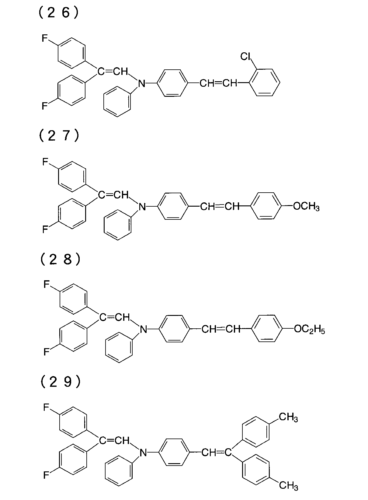
Specific examples of the organic photoconductive material represented by the general formula (1) of the present invention include those having the following structural formula, but are not limited thereto.
[0018]
[Chemical 3]
[Formula 4]
[Chemical formula 5]
[Chemical 6]
[Chemical 7]
[Chemical 8]
[Chemical 9]
[Chemical Formula 10]
Embedded image
Embedded image
Embedded image
Embedded image
The electrophotographic photosensitive member of the present invention can be obtained by containing one or more organic photoconductive materials and charge generating materials represented by the general formula (1). The charge generation material includes an inorganic charge generation material and an organic charge generation material. Examples of the former include selenium, selenium-tellurium alloy, selenium-arsenic alloy, cadmium sulfide, zinc oxide, and amorphous silicon. Examples of organic charge generating materials include triphenylmethane dyes such as methyl violet, brilliant green and crystal violet, thiazine dyes such as methylene blue, quinone dyes such as quinizarin, cyanine dyes, acridine dyes, pyrylium dyes, thiapyrylium dyes , Squalium dyes, perinone pigments, anthraquinone pigments, metal-containing or metal-free phthalocyanine pigments, perylene pigments, and the like, and azo pigments are also used.
[0031]
As phthalocyanines, many compounds are known as general color materials or electrophotographic pigments, and any of these compounds can be used in the present invention. Specific examples thereof include, for example, JP-A-51-108847, JP-A-51-117637, JP-A-56-69644, JP-A-57-111149, JP-A-58-158649, and JP-A-58-215655. 59-44053, 59-44054, 59-128544, 59-133550, 59-133551, 59-174844, 60-2061, 61-203461, 61-2117050, 62-275272, 62-296150, 63-17457, 63-286857, 63-95460, Special Japanese Laid-Open Patent Publication No. 1-144057, Japanese Laid-Open Patent Publication No. 64-38753, Japanese Laid-Open Patent Publication No. 1-2204968, No. 1-221459, No. 1-2247469, No. 1-226863, No. 1-312551, No. 2-289657, No. 3-227372, No. 4-277562, No. 4 Phthalocyanine compounds described in JP-A-360150, JP-A-5-45914, JP-A-5-66594, JP-A-5-93366, and JP-A-7-53892.
[0032]
Examples of the azo pigment include JP-A-47-37543, JP-A-53-95033, JP-A-53-132347, JP-A-53-133445, JP-A-54-12742, and JP-A-54-. 20736, JP 54-20737, JP 54-21728, JP 54-22234, JP 55-69148, JP 55-69654, JP 55-79449 JP-A-55-117151, JP-A-56-46237, JP-A-56-1116039, JP-A-56-11040, JP-A-56-119134, JP-A-56-143437, JP-A-57-63537, JP-A-57-63538, JP-A-57-63541, JP-A-57-63542, JP-A-57-63549, JP-A-57-66438, JP-A-57-66438 57-74746, JP 57-78542, JP 57-78543, JP 57-90056, JP 57-90057, JP 57-90632, JP 57- 116345, JP 57-202349, JP 58-4151, JP 58-90644, JP 58-144358, JP 58-177955, JP 59-31962. JP-A-59-33253, JP-A-59-71059, JP-A-59-72448, JP-A-59-78356, JP-A-59-136351, JP-A-59-201060, JP 60-15642, JP 60-14351, JP 60-179746, JP 61-11754, JP 61-90164, JP 61-90165, JP 1-90166, JP 61-112154, JP 61-281245, JP 61-51063, JP 62-267363, JP 63-68844, JP 63- 89866, JP 63-139355, JP 63-142033, JP 63-183450, JP 63-282743, JP 64-21455, JP 64-78259 JP-A-1-200267, JP-A-1-202757, JP-A-1-319754, JP-A-2-72372, JP-A-2-254467, JP-A-3-27863, JP-A-4-96068, JP-A-4-96069, JP-A-4-147265, JP-A-5-142841, JP-A-5-303226, JP-A-6-324504, JP-A-7-168 379, JP-A-9-297414, JP-A-9-297416, and the like.
[0033]
Moreover, the structure of the coupler component used for these azo pigments varies widely. For example, JP-A-54-17735, JP-A-54-79632, JP-A-57-176055, JP-A-59-97043, JP-A-60-130746, JP-A-60-153050, Japanese Unexamined Patent Publication Nos. 60-103048, 60-189759, 63-131146, 63-155052, 2-110569, 4-149448, and 6-272705. And compounds described in JP-A-6-348047.
[0034]
Various types of photoreceptors are known, and any of them can be used. For example, there is one in which a photosensitive layer made of a charge generating substance, a charge transporting substance, and a film-forming binder resin is provided on a conductive support. There is also known a laminated type photoreceptor in which a charge generation layer made of a charge generation material and a binder resin and a charge transport layer made of a charge transport material and a binder resin are provided on a conductive support. . Either the charge generation layer or the charge transport layer may be an upper layer. If necessary, an undercoat layer is provided between the conductive support and the photosensitive layer, an overcoat layer is provided on the surface of the photosensitive member, and in the case of a laminated type photosensitive member, an intermediate layer is provided between the charge generation layer and the charge transporting layer. Can also be provided. As a support for producing a photoreceptor using the compound of the present invention, a metal drum, a metal plate, a paper subjected to conductive processing, a sheet of plastic film, a drum or a belt, and the like are used. .
[0035]
Various film-forming binder resins used for forming a photosensitive layer on such a support may be used depending on the application field. For example, in the use of photoconductors for copying, polystyrene resin, polyvinyl acetal resin, polysulfone resin, polycarbonate resin, vinyl acetate / crotonic acid copolymer resin, polyester resin, polyphenylene oxide resin, polyarylate resin, alkyd resin, acrylic resin, methacrylic resin And phenoxy resin. Among these, polystyrene resin, polyvinyl acetal resin, polycarbonate resin, polyester resin, polyarylate resin, and the like are excellent in potential characteristics as a photoreceptor. These resins can be used alone or as a copolymer in combination of one or more. The amount of the binder resin added to the photoconductive compound is preferably 20 to 1000% by weight, and more preferably 50 to 500% by weight.
[0036]
In the case of a multilayer photoreceptor, these resins contained in the charge generation layer are preferably 10 to 500% by weight, more preferably 50 to 150% by weight, based on the charge generation material. If the resin ratio is too high, the charge generation efficiency is lowered, and if the resin ratio is too low, there is a problem in film formability. In addition, these resins contained in the charge transport layer are preferably 20 to 1000% by weight, more preferably 50 to 500% by weight with respect to the charge transport material. If the ratio of the resin is too high, the sensitivity is lowered, and if the ratio of the resin is too low, the repeated characteristics may be deteriorated or the coating film may be lost.
[0037]
Some of these resins are weak in mechanical strength such as pulling, bending, and compression. To improve this property, a plasticizing substance can be added. Specific examples include phthalic acid esters (for example, DOP and DBP), phosphoric acid esters (for example, TCP and TOP), sebacic acid esters, adipic acid esters, nitrile rubber, chlorinated hydrocarbons, and the like. When these substances are added more than necessary, the electrophotographic characteristics are adversely affected, and therefore the ratio is preferably 20% or less with respect to the binder resin.
[0038]
In addition, a leveling agent or the like can be added as necessary to improve the coatability, such as an antioxidant or an anti-curl agent, as additives in the photoreceptor.
[0039]
The compound represented by the general formula (1) can be used in combination with another charge transporting substance. Charge transport materials include hole transport materials and electron transport materials. Examples of the former include, for example, oxadiazoles disclosed in Japanese Patent Publication No. 34-5466, triphenylmethanes disclosed in Japanese Patent Publication No. 45-555, and Japanese Patent Publication No. 52-4188. And the like, hydrazones shown in JP-B-55-42380, oxadiazoles shown in JP-A-56-123544, and the like. On the other hand, examples of the electron transport material include chloranil, tetracyanoethylene, tetracyanoquinodimethane, 2,4,7-trinitro-9-fluorenone, 2,4,5,7-tetranitro-9-fluorenone, 2,4 , 5,7-tetranitroxanthone, 2,4,8-trinitrothioxanthone, 1,3,7-trinitrodibenzothiophene, 1,3,7-trinitrodibenzothiophene-5,5-dioxide. These charge transport materials can be used alone or in combination of two or more.
[0040]
In addition, a certain electron-withdrawing compound may be added as a sensitizer that forms a charge transfer complex with the organic conductive material of the present invention and further enhances the sensitizing effect. Examples of the electron-withdrawing compound include quinones such as 2,3-dichloro-1,4-naphthoquinone, 1-nitroanthraquinone, 1-chloro-5-nitroanthraquinone, 2-chloroanthraquinone, and phenanthrenequinone, 4-nitro Aldehydes such as benzaldehyde, ketones such as 9-benzoylanthracene, indandione, 3,5-dinitrobenzophenone, 3,3 ', 5,5'-tetranitrobenzophenone, phthalic anhydride, 4-chloronaphthalic anhydride, etc. Acid anhydrides, terephthalalmalononitrile, 9-anthrylmethylidenemalononitrile, 4-nitrobenzalmalononitrile, cyano compounds such as 4- (p-nitrobenzoyloxy) benzalmalononitrile, 3-benzalphthalide, 3 -(Α-cyano-p-nitrobenza ) Phthalide, 3- (alpha-cyano -p- Nitorobenzaru) -4,5,6,7 can be mentioned phthalides such as tetrachloro phthalide like.
[0041]
The organic photoconductive material of the present invention is dissolved or dispersed in an appropriate solvent together with the above-mentioned various additives depending on the form of the photoreceptor, and the coating solution is applied onto the conductive support described above. The photosensitive member can be manufactured by drying.
[0042]
As coating solvents, halogenated hydrocarbons such as chloroform, dichloroethane, dichloromethane, trichloroethane, trichloroethylene, chlorobenzene, dichlorobenzene, aromatic hydrocarbons such as benzene, toluene, xylene, dioxane, tetrahydrofuran, methyl cellosolve, ethyl cellosolve, ethylene glycol dimethyl ether Ether solvents such as methyl ethyl ketone, methyl isobutyl ketone, methyl isopropyl ketone, cyclohexanone, etc., ester solvents such as ethyl acetate, methyl formate, methyl cellosolve acetate, N, N-dimethylformamide, acetonitrile, N-methyl Aprotic polar solvents such as pyrrolidone and dimethyl sulfoxide, and methanol, ethanol, propanol, butanol, etc. It may be mentioned alcohol-based solvents. These solvents can be used alone or as a mixed solvent of two or more.
[0043]
【Example】
EXAMPLES Next, although an Example demonstrates this invention still in detail, this invention is not limited to these at all.
[0044]
Synthesis Example Synthesis of Exemplified Compound (18)
a) Synthesis of intermediate enamine compound (50)
Embedded image
25.09 g of 4,4′-difluorobenzophenone, 14.80 g of ethyl chloroacetate and 23 ml of 1,3-dioxolane were mixed at room temperature. A suspension prepared by mixing 15.48 g of separately prepared potassium tert-butoxide and 69 ml of 1,3-dioxolane was added dropwise to the mixture under ice-cooling and stirring. At this time, heat generation was observed, but the internal temperature was maintained at 20 ° C. or lower by adjusting the dropping rate. After completion of the dropwise addition, the reaction was completed by further stirring at room temperature for 1 hour. Next, 22.20 g of sodium methoxide (28% methanol solution) was added dropwise to the reaction mixture with stirring under ice cooling. At this point no noticeable exotherm was observed. Next, 2.8 g of water was added dropwise with stirring on ice. Although heat generation was observed at this point, the internal temperature was maintained at 20 ° C. or lower by adjusting the dropping rate. The mixture was further stirred at room temperature for 1 hour to complete the reaction, and then concentrated under reduced pressure to obtain sodium 3,3-bis (4-fluorophenyl) -2,3-epoxypropionate.
[0047]
The sodium salt obtained above was suspended in 69 ml of water, and 13.8 ml of concentrated hydrochloric acid was added dropwise with stirring at room temperature. The internal temperature rose due to the dropwise addition of concentrated hydrochloric acid, and foaming due to decarboxylation was observed. After completion of dropping, the reactor was heated and stirred in a 90 ° C. hot water bath for 1 hour to complete the reaction. After allowing to cool, the organic component was extracted with toluene, and the extract was washed successively with water and saturated brine. After drying over anhydrous sodium sulfate, the mixture was concentrated under reduced pressure to obtain 2,2-bis (4-fluorophenyl) acetaldehyde as a pale yellow oil.
[0048]
Mix the aldehyde compound obtained above with 19.46 g of diphenylamine, 0.22 g of p-toluenesulfonic acid monohydrate and 140 ml of toluene, and heat for 1 hour while dehydrating azeotropically with a Dean-Stark trap. Refluxed. After allowing to cool, toluene was removed under reduced pressure, and the precipitated crystals were suspended in 150 ml of 2-propanol and washed with heating. After allowing to cool, the crystals were collected by filtration and washed with 2-propanol on the funnel to obtain 35.24 g of an intermediate enamine compound (50) as white crystals. The yield in 4 steps from 4,4'-difluorobenzophenone was 79.9%.
Melting point: 144.1-144.5 ° C
1 H-NMR (CDCl 3 ) δ 6.65 to 6.70 ppm (m, 3H), δ 6.84 to 7.00 ppm (m, 10H), δ 7.08 to 7.19 ppm (m, 6H) 13 C-NMR (CDCl 3 ) δ 114.32 ppm, δ 114.66 ppm, δ 114.88 ppm, δ 115.22 ppm, δ 122.36 ppm, δ 122.91 ppm, δ 127.83 ppm, δ 128.68 ppm, δ 128.83 ppm, δ 131.15 ppm, δ 131.36 ppm, δ 131. 49ppm, δ134.72ppm, δ134.78ppm, δ137.91ppm, δ137.95ppm, δ145.53ppm, δ159.47ppm, δ160.09ppm, δ163.37ppm, δ164.00ppm
[0049]
b) Synthesis of intermediate aldehyde compound (51)
Embedded image
To 32.5 ml of N, N-dimethylformamide, 13.0 ml of phosphorus oxychloride was added dropwise with stirring under ice cooling while keeping the internal temperature at 15 ° C. or lower. The solution was further stirred at room temperature for 30 minutes, 26.8 g of the intermediate enamine compound (50) obtained above and 70 ml of N, N-dimethylformamide were added, and the mixture was stirred with heating at an internal temperature of about 80 ° C. for 4 hours. did. After allowing to cool, the reaction solution was diluted with 500 ml of ice water and hydrolyzed by stirring with heating at an internal temperature of about 35 ° C. for 1 hour. The organic component precipitated after being allowed to cool was extracted with toluene, washed successively with water, dilute aqueous sodium bicarbonate and saturated brine, and then dried over anhydrous sodium sulfate. After drying, sodium sulfate was removed by filtration and concentrated under reduced pressure to obtain yellowish white crystals. The obtained crystal was recrystallized from isopropyl alcohol to obtain 21.5 g of an intermediate aldehyde compound (51). The yield was 78.4%. Melting point: 130.7-131.0 ° C.
[0052]
c) Synthesis of Exemplified Compound (18) 3.28 g of the raw material aldehyde compound (51) obtained above, 1.92 g of diethyl benzylphosphonate and 10 ml of 1,3-dioxolane were mixed at room temperature. To this mixed solution, 1.35 g of potassium tert-butoxide was added little by little with ice-cooling, and stirring was further continued at room temperature for 1 hour after the addition was completed. 50 ml of water was added to the reaction solution, and the precipitated organic component was extracted with toluene, and washed successively with dilute sodium bicarbonate water, water, and saturated brine. After drying over anhydrous sodium sulfate and concentrating under reduced pressure, 15 ml of ethanol was added to the resulting oily product and allowed to stand overnight. The precipitated crystals were collected by filtration, and the obtained crystals were recrystallized with a mixed solvent of ethyl acetate and isopropyl alcohol to obtain 2.72 g of Exemplified Compound (18). The yield was 71.1%. Melting point: 142.8-143.3 ° C.
[0053]
The structural formulas of the azo pigments used in the examples are shown below.
[0054]
Embedded image
Embedded image
Example 1
1 part by weight of an azo pigment (52) and 1 part by weight of a polyester resin (Toyobo Byron 200) were mixed with 100 parts by weight of tetrahydrofuran and dispersed with glass beads in a paint conditioner device for 2 hours. The dispersion thus obtained was applied onto an aluminum vapor-deposited polyester with an applicator and dried to form a charge generation layer having a thickness of about 0.2 μm. Next, Exemplified Compound (18) is mixed with polyarylate resin (Unitika U-polymer) at a weight ratio of 1: 1 to make a 10% solution using dichloroethane as a solvent, and an applicator is formed on the charge generation layer. Was applied to form a charge transport layer having a thickness of about 20 μm.
[0057]
The multilayer photoconductor produced in this manner was evaluated for electrophotographic characteristics using an electrostatic recording test apparatus (SP-428 manufactured by Kawaguchi Electric).
Measurement conditions: applied voltage -6 kV, static No. 3 (turn table rotation speed mode: 10 m / min). As a result, the charging potential (Vo) was -850 V, and the half exposure amount (E1 / 2) was 0.9 lux.sec.
[0058]
Further, using the same apparatus, the characteristics were evaluated for repeated use with one cycle of charge-static elimination (static elimination light: 400 lux × 1 second irradiation with white light). When the change of the charging potential by repeating 5000 times was obtained, the charging potential (Vo) of 5000 times was -840V with respect to the charging potential (Vo) of -850V of the first time, and there was no decrease in potential due to repetition. Showed the characteristics. In addition, the first half-exposure dose (E1 / 2) was 0.9 lux.sec. And the 5000th half-exposure dose (E1 / 2) was 0.9 lux.sec. .
[0059]
Examples 2-9
A photoconductor was prepared in the same manner as in Example 1 except that the azo pigment and the exemplified compound shown in Table 1 were used instead of the azo pigment (52) and the exemplified compound (18) of Example 1, respectively. evaluated. The results are shown in Table 1.
[0060]
[Table 1]
Examples 10-18
A photoconductor was prepared in the same manner as in Example 1 except that the X-type metal-free phthalocyanine was used in place of the azo pigment of Example 1 and the exemplified compound shown in Table 2 was used in place of the exemplified compound (18). Characteristics were evaluated. The results are shown in Table 2.
[0062]
[Table 2]
Example 19
One part by weight of the azo pigment (52) and 40 parts by weight of tetrahydrofuran were dispersed with a glass bead for 4 hours using a paint conditioner device. 2.5 parts by weight of Exemplified Compound (18), 10 parts by weight of a polycarbonate resin (PCZ-200; manufactured by Mitsubishi Gas Chemical), and 60 parts by weight of tetrahydrofuran are added to the dispersion thus obtained, and the mixture is further treated with a paint conditioner for 30 minutes. After carrying out the dispersion treatment, it was applied on aluminum vapor-deposited polyester with an applicator to form a photoreceptor having a film thickness of about 15 μm. The electrophotographic characteristics of this photoreceptor were evaluated in the same manner as in Example 1. However, only the applied voltage was changed to +5 kV. As a result, the first charging potential (Vo) +450 V, half-exposure amount (E1 / 2) 1.3 lux.sec., Charging potential (Vo) after repeating 5000 times + 435 V, half-exposure amount (E1 / 2) 1 Excellent characteristics with high sensitivity and little change of 2 lux / second.
[0064]
Examples 20-27
A photoconductor was prepared in the same manner as in Example 19 except that the azo pigment and exemplary compound shown in Table 3 were used instead of the azo pigment (52) and exemplary compound (18) of Example 19, respectively. evaluated. The results are shown in Table 3.
[0065]
[Table 3]
Comparative Example 1
A photoconductor was prepared in the same manner as in Example 1 except that the following comparative compound (58) was used instead of the exemplified compound (18), and the characteristics thereof were evaluated. As a result, the first charging potential (Vo) is -720V, the half exposure amount (E1 / 2) is as low as 2.0 lux.sec, and the 5000th charging potential (Vo) is -505V, half exposure. The amount (E1 / 2) was 1.7 lux · second, and a significant decrease in potential due to repetition was observed.
[0067]
Comparative Example 2
A photoreceptor was prepared in the same manner as in Example 10 except that the following comparative compound (59) was used in place of the exemplified compound (18), and the characteristics thereof were evaluated. As a result, the first charging potential (Vo) was -725 V, and the half exposure amount (E1 / 2) was relatively good, 1.3 lux.sec, but the 5000th charging potential (Vo) was -325V, half-exposure dose (E1 / 2) 1.0 lux.sec. A significant decrease in potential due to repetition was observed.
[0068]
Comparative Example 3
A photoconductor was prepared in the same manner as in Example 19 except that the following comparative compound (60) was used instead of the exemplified compound (18), and its characteristics were evaluated. As a result, the charged potential (Vo) was 365 V, and the half exposure amount (E1 / 2) was 6.6 lux · sec.
[0069]
Embedded image
【The invention's effect】
As is clear from the above, an electrophotographic photosensitive member having high sensitivity and high durability can be provided by using the organic photoconductive material of the present invention.
Claims (3)
Priority Applications (1)
| Application Number | Priority Date | Filing Date | Title |
|---|---|---|---|
| JP01264198A JP3649890B2 (en) | 1998-01-26 | 1998-01-26 | Organic photoconductive material and electrophotographic photoreceptor using the same |
Applications Claiming Priority (1)
| Application Number | Priority Date | Filing Date | Title |
|---|---|---|---|
| JP01264198A JP3649890B2 (en) | 1998-01-26 | 1998-01-26 | Organic photoconductive material and electrophotographic photoreceptor using the same |
Publications (2)
| Publication Number | Publication Date |
|---|---|
| JPH11212282A JPH11212282A (en) | 1999-08-06 |
| JP3649890B2 true JP3649890B2 (en) | 2005-05-18 |
Family
ID=11811003
Family Applications (1)
| Application Number | Title | Priority Date | Filing Date |
|---|---|---|---|
| JP01264198A Expired - Fee Related JP3649890B2 (en) | 1998-01-26 | 1998-01-26 | Organic photoconductive material and electrophotographic photoreceptor using the same |
Country Status (1)
| Country | Link |
|---|---|
| JP (1) | JP3649890B2 (en) |
Families Citing this family (1)
| Publication number | Priority date | Publication date | Assignee | Title |
|---|---|---|---|---|
| JP5355984B2 (en) * | 2008-10-23 | 2013-11-27 | 京セラドキュメントソリューションズ株式会社 | Electrophotographic photoreceptor and image forming apparatus provided with the same |
-
1998
- 1998-01-26 JP JP01264198A patent/JP3649890B2/en not_active Expired - Fee Related
Also Published As
| Publication number | Publication date |
|---|---|
| JPH11212282A (en) | 1999-08-06 |
Similar Documents
| Publication | Publication Date | Title |
|---|---|---|
| JP3685581B2 (en) | Organic photoconductive material and electrophotographic photoreceptor using the same | |
| JP3587942B2 (en) | Organic photoconductive material and electrophotographic photoreceptor using the same | |
| JP3703289B2 (en) | Organic photoconductive material and electrophotographic photoreceptor using the same | |
| JP2690541B2 (en) | Electrophotographic photoreceptor | |
| JP3649890B2 (en) | Organic photoconductive material and electrophotographic photoreceptor using the same | |
| JP3730025B2 (en) | Organic photoconductive compound and electrophotographic photoreceptor using the same | |
| JP3736910B2 (en) | Organic photoconductive material and electrophotographic photoreceptor using the same | |
| JP3714898B2 (en) | Organic photoconductive material and electrophotographic photoreceptor using the same | |
| JPH09297416A (en) | Organic photoconductive material and electrophotographic photoreceptor using the same | |
| JP3556391B2 (en) | Organic photoconductive material and electrophotographic photoreceptor using the same | |
| JP3640756B2 (en) | Organic photoconductive material and electrophotographic photoreceptor using the same | |
| JP4170840B2 (en) | Electrophotographic photoreceptor | |
| JP4162807B2 (en) | Organic photoconductive compound and electrophotographic photoreceptor using the same | |
| JP4489891B2 (en) | Alkenylamine compound and electrophotographic photosensitive member using the same | |
| JP4162808B2 (en) | Organic photoconductive compound and electrophotographic photoreceptor using the same | |
| JP3290875B2 (en) | Electrophotographic photoreceptor, and method for producing bisazo compound, intermediate and bisazo compound | |
| JPH1063019A (en) | Organic photoconductive material and electrophotographic photoreceptor using the same | |
| JP3587941B2 (en) | Organic photoconductive material and electrophotographic photoreceptor using the same | |
| JP3842911B2 (en) | Distilbene compound and electrophotographic photosensitive member using the same | |
| JP4198836B2 (en) | Organic photoconductive compound and electrophotographic photoreceptor using the same | |
| JP2914462B2 (en) | Electrophotographic photoreceptor | |
| JP4343605B2 (en) | Enamine-bis (hydroxyarylene-substituted) polyene compound and production intermediate thereof | |
| JP4275655B2 (en) | Organic photoconductive compound and electrophotographic photoreceptor using the same | |
| JP3649846B2 (en) | Organic photoconductive material and electrophotographic photoreceptor using the same | |
| JP3130154B2 (en) | Electrophotographic photoreceptor |
Legal Events
| Date | Code | Title | Description |
|---|---|---|---|
| TRDD | Decision of grant or rejection written | ||
| A01 | Written decision to grant a patent or to grant a registration (utility model) |
Free format text: JAPANESE INTERMEDIATE CODE: A01 Effective date: 20050215 |
|
| A61 | First payment of annual fees (during grant procedure) |
Free format text: JAPANESE INTERMEDIATE CODE: A61 Effective date: 20050216 |
|
| R150 | Certificate of patent or registration of utility model |
Free format text: JAPANESE INTERMEDIATE CODE: R150 |
|
| S111 | Request for change of ownership or part of ownership |
Free format text: JAPANESE INTERMEDIATE CODE: R313113 |
|
| R350 | Written notification of registration of transfer |
Free format text: JAPANESE INTERMEDIATE CODE: R350 |
|
| FPAY | Renewal fee payment (event date is renewal date of database) |
Free format text: PAYMENT UNTIL: 20080225 Year of fee payment: 3 |
|
| S531 | Written request for registration of change of domicile |
Free format text: JAPANESE INTERMEDIATE CODE: R313531 |
|
| FPAY | Renewal fee payment (event date is renewal date of database) |
Free format text: PAYMENT UNTIL: 20080225 Year of fee payment: 3 |
|
| R350 | Written notification of registration of transfer |
Free format text: JAPANESE INTERMEDIATE CODE: R350 |
|
| FPAY | Renewal fee payment (event date is renewal date of database) |
Free format text: PAYMENT UNTIL: 20080225 Year of fee payment: 3 |
|
| FPAY | Renewal fee payment (event date is renewal date of database) |
Free format text: PAYMENT UNTIL: 20090225 Year of fee payment: 4 |
|
| FPAY | Renewal fee payment (event date is renewal date of database) |
Free format text: PAYMENT UNTIL: 20100225 Year of fee payment: 5 |
|
| FPAY | Renewal fee payment (event date is renewal date of database) |
Free format text: PAYMENT UNTIL: 20110225 Year of fee payment: 6 |
|
| FPAY | Renewal fee payment (event date is renewal date of database) |
Free format text: PAYMENT UNTIL: 20120225 Year of fee payment: 7 |
|
| FPAY | Renewal fee payment (event date is renewal date of database) |
Free format text: PAYMENT UNTIL: 20130225 Year of fee payment: 8 |
|
| S531 | Written request for registration of change of domicile |
Free format text: JAPANESE INTERMEDIATE CODE: R313531 |
|
| FPAY | Renewal fee payment (event date is renewal date of database) |
Free format text: PAYMENT UNTIL: 20130225 Year of fee payment: 8 |
|
| R350 | Written notification of registration of transfer |
Free format text: JAPANESE INTERMEDIATE CODE: R350 |
|
| FPAY | Renewal fee payment (event date is renewal date of database) |
Free format text: PAYMENT UNTIL: 20130225 Year of fee payment: 8 |
|
| FPAY | Renewal fee payment (event date is renewal date of database) |
Free format text: PAYMENT UNTIL: 20140225 Year of fee payment: 9 |
|
| LAPS | Cancellation because of no payment of annual fees |