JP3647166B2 - Power circuit - Google Patents
Power circuit Download PDFInfo
- Publication number
- JP3647166B2 JP3647166B2 JP26120896A JP26120896A JP3647166B2 JP 3647166 B2 JP3647166 B2 JP 3647166B2 JP 26120896 A JP26120896 A JP 26120896A JP 26120896 A JP26120896 A JP 26120896A JP 3647166 B2 JP3647166 B2 JP 3647166B2
- Authority
- JP
- Japan
- Prior art keywords
- output
- voltage
- value
- power supply
- control
- Prior art date
- Legal status (The legal status is an assumption and is not a legal conclusion. Google has not performed a legal analysis and makes no representation as to the accuracy of the status listed.)
- Expired - Fee Related
Links
Images


Classifications
-
- H—ELECTRICITY
- H02—GENERATION; CONVERSION OR DISTRIBUTION OF ELECTRIC POWER
- H02M—APPARATUS FOR CONVERSION BETWEEN AC AND AC, BETWEEN AC AND DC, OR BETWEEN DC AND DC, AND FOR USE WITH MAINS OR SIMILAR POWER SUPPLY SYSTEMS; CONVERSION OF DC OR AC INPUT POWER INTO SURGE OUTPUT POWER; CONTROL OR REGULATION THEREOF
- H02M3/00—Conversion of dc power input into dc power output
- H02M3/22—Conversion of dc power input into dc power output with intermediate conversion into ac
- H02M3/24—Conversion of dc power input into dc power output with intermediate conversion into ac by static converters
- H02M3/28—Conversion of dc power input into dc power output with intermediate conversion into ac by static converters using discharge tubes with control electrode or semiconductor devices with control electrode to produce the intermediate ac
- H02M3/325—Conversion of dc power input into dc power output with intermediate conversion into ac by static converters using discharge tubes with control electrode or semiconductor devices with control electrode to produce the intermediate ac using devices of a triode or a transistor type requiring continuous application of a control signal
- H02M3/335—Conversion of dc power input into dc power output with intermediate conversion into ac by static converters using discharge tubes with control electrode or semiconductor devices with control electrode to produce the intermediate ac using devices of a triode or a transistor type requiring continuous application of a control signal using semiconductor devices only
- H02M3/33507—Conversion of dc power input into dc power output with intermediate conversion into ac by static converters using discharge tubes with control electrode or semiconductor devices with control electrode to produce the intermediate ac using devices of a triode or a transistor type requiring continuous application of a control signal using semiconductor devices only with automatic control of the output voltage or current, e.g. flyback converters
-
- H—ELECTRICITY
- H02—GENERATION; CONVERSION OR DISTRIBUTION OF ELECTRIC POWER
- H02M—APPARATUS FOR CONVERSION BETWEEN AC AND AC, BETWEEN AC AND DC, OR BETWEEN DC AND DC, AND FOR USE WITH MAINS OR SIMILAR POWER SUPPLY SYSTEMS; CONVERSION OF DC OR AC INPUT POWER INTO SURGE OUTPUT POWER; CONTROL OR REGULATION THEREOF
- H02M3/00—Conversion of dc power input into dc power output
- H02M3/22—Conversion of dc power input into dc power output with intermediate conversion into ac
- H02M3/24—Conversion of dc power input into dc power output with intermediate conversion into ac by static converters
- H02M3/28—Conversion of dc power input into dc power output with intermediate conversion into ac by static converters using discharge tubes with control electrode or semiconductor devices with control electrode to produce the intermediate ac
- H02M3/325—Conversion of dc power input into dc power output with intermediate conversion into ac by static converters using discharge tubes with control electrode or semiconductor devices with control electrode to produce the intermediate ac using devices of a triode or a transistor type requiring continuous application of a control signal
- H02M3/335—Conversion of dc power input into dc power output with intermediate conversion into ac by static converters using discharge tubes with control electrode or semiconductor devices with control electrode to produce the intermediate ac using devices of a triode or a transistor type requiring continuous application of a control signal using semiconductor devices only
- H02M3/33569—Conversion of dc power input into dc power output with intermediate conversion into ac by static converters using discharge tubes with control electrode or semiconductor devices with control electrode to produce the intermediate ac using devices of a triode or a transistor type requiring continuous application of a control signal using semiconductor devices only having several active switching elements
-
- H—ELECTRICITY
- H02—GENERATION; CONVERSION OR DISTRIBUTION OF ELECTRIC POWER
- H02M—APPARATUS FOR CONVERSION BETWEEN AC AND AC, BETWEEN AC AND DC, OR BETWEEN DC AND DC, AND FOR USE WITH MAINS OR SIMILAR POWER SUPPLY SYSTEMS; CONVERSION OF DC OR AC INPUT POWER INTO SURGE OUTPUT POWER; CONTROL OR REGULATION THEREOF
- H02M3/00—Conversion of dc power input into dc power output
- H02M3/01—Resonant DC/DC converters
Landscapes
- Engineering & Computer Science (AREA)
- Power Engineering (AREA)
- Dc-Dc Converters (AREA)
Description
【0001】
【発明の属する技術分野】
本発明は、トランス(多出力巻線トランス或いは高圧トランス)を含む電源回路に関する。
【0002】
【従来の技術】
従来、複写機等の静電方式画像形成装置の電源システムとして、装置の論理回路動作用またはモーター、ソレノイド等の電力供給用低圧出力と静電方式画像形成用高圧出力を1つのトランスで動作させるものが提案及び実用化されている。
【0003】
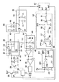
以下、この種の電源システムの従来例として、複写機に搭載される複合型電源回路のブロック構成を図18に示す。同図において、1は商用AC電源、2は整流ブリッジ、3は第1の平滑コンデンサ、4は入力巻線駆動用スイッチング素子、5は共振コンデンサで、後述する複合型トランス20の入力インダクタンス成分とにより電圧共振を発生させる役割を持つ。6はクランプダイオード、7はカレントランスで、入力巻線駆動用のスイッチング素子4、共振コンデンサ5及びクランプダイオード6を流れる電流をモニターするためのトランスである。8はドライブトランスで、二次側にある主制御部9からのスイッチング素子駆動信号を一時側に伝達するためのトランスである。主制御部9は、低圧用フライバック巻線22の整流出力電圧の検出結果に基づいて一次巻線21のオン動作時間を制御し、該低圧用フライバック巻線22の整流出力電圧を所定値に制御するものである。主制御部9は、スイッチング素子4の駆動信号出力部9a、一次側駆動電流検出信号入力部9b及び24VR平滑電圧検出信号入力部9cを有している。
【0004】
また、図18において、10は低圧用フライバック巻線22の出力を整流するダイオード、11は平滑コンデンサである。本例における本出力は24Vに制御するものとし、24VRと称する。12は24VRの電圧を検出するための電圧検出抵抗、13は低圧用フォワード巻線23の出力を整流するダイオード、14はスイッチング素子で、低圧用フォワード巻線23の平滑出力が所定値となるようにオン/オフ動作する。本例における本出力は24Vに制御するものとし、24VUと称する。15はフライホイールダイオード、16は整流用インダクタンス、17は平滑コンデンサ、18は24VU出力を検出するための出力検出抵抗、19は副制御部で、24VU出力が所定値となるようにスイッチング素子14の導通角を制御するものである。副制御部19は、24VU用スイッチング素子14の駆動信号出力部19a、24VU平滑出力検出信号入力部19b及びスイッチング素子4の駆動信号入力部19cを有している。
【0005】
更に、図18において、20は複合型トランスで、一次巻線21、低圧用フライバック巻線22、低圧用フォワード巻線23及び高圧用巻線24,25を有している。26はダイオードで、高圧用巻線24の出力を負電圧に整流する。27は平滑コンデンサ、28はダイオードで、高圧用巻線25の出力を正電圧に整流する。29は平滑コンデンサである。
【0006】
次に、上記構成の電源回路の動作を説明する。
【0007】
商用AC電源1からの電流は整流ブリッジ2及び平滑コンデンサ3により整流平滑されて複合型トランス20の一次巻線21の一端に入る。スイッチング素子4がオンの間、該スイッチング素子4に流れる電流は複合型トランス20の入力インダクタンスに反比例した傾きで直線的に増加する。また、24VU巻線出力のスイッチング素子14がオンとなっている期間は、その巻線電流が巻数比に反比例して一次側スイッチング素子4に重畳される。
【0008】
次に、一次側スイッチング素子4がオフすると、その際の電流エネルギーを基に、一次側インダクタンスと共振コンデンサ5によるLC共振が発生する。共振コンデンサ5の電圧は概略正弦波となり、増加し、ピークを迎えた後、減少する。このときクランプタイオード6によって負側はダイオード順方向電圧に制限される。主制御部9は、この様子をカレントランス7によりモニターし、負側に電流が振れ込むのを検知した瞬間、スイッチング素子4に対して再びオン信号を発生する。複合型トランス20の低圧用フライバック巻線22は、この共振ピーク値側の位相で整流平滑され、この電圧が主制御部9によりモニターされる。二次側にある主制御部9は、24Vよりも低い場合は、スイッチング素子4のオン幅を増やし、高い場合は減らす。
【0009】
以上により、スイッチング素子4に対しては常に0ボルトでのスイッチングが実現され、また低圧用フライバック巻線22の整流平滑電圧が24Vに制御される。一方、他の出力巻線は、複合型トランス20の巻数比に応じた出力電圧が出力される。
【0010】
以上のように、複合型トランス20の入力側においてLCフライバック電圧共振を発生させ、出力側にて1つの低圧用フライバック巻線22の出力のピーク整流値を所定値に制御することにり、複合型トランス20の高圧出力巻線24,25にはフライバック側のピーク値を一定値に制御した高圧出力が発生することとなる。
【0011】
なお、主制御部9は、一般的には24VRの制御目標電圧を時間的に漸次上昇させ、24VRの最終目標値への立ち上がりに所定時間をかける、所謂ソフトスタート機能を付加し、関係各部品の過渡的な電流、電圧負担を軽減するのが通例である。
【0012】
24VU巻線出力は、所謂フォワード側の出力を平滑する向きとなっており、一般的には24VRに比べ出力電圧を大きくとることができるが、複合型トランス20の各巻線のフォワード側電圧はAC入力電圧の平滑電圧に概略比例するため、出力電圧に対する要求制度によっては二次側での個別の電圧制御が必要となる。24VU電圧制御部(副制御部)19は、24VU電流電圧をモニターし、スイッチング素子14の導通率を変化させ、所定の電圧に制御する。
【0013】
定常時の主要な動作波形を図19に示す。同図は、24VUの外部負荷がオン状態になった際の定常動作を示す。
【0014】
図19において、(a)はMPWMの動作波形、(b)はスイッチング素子4のコレクタ電圧の動作波形、(c)はスイッチング素子4のコレクタ電流の動作波形、(d)は24VUSW(スイッチング素子14)制御信号の動作波形である。
【0015】
また、従来より、複写機等の静電方式の電子写真画像形成装置においては、感光体への帯電、現像、転写紙への転写、転写紙の感光体からの分離等の目的で、数百ボルト(v)から数十キロボルト(kv)程度の出力を行う数種の高圧電源回路を具備している。
【0016】
これらは、その目的に応じて外部制御装置より所定のオン/オフ信号、出力電圧制御信号、出力電流制御信号を受け取り出力の制御を行うが、近年、画像形成条件のよりきめ細かな最適化の流れとして、帯電装置、転写装置等、それぞれの高圧出力負荷の電気的なインピーダンスによって出力電圧値をより最適な値へと切り換えたいという要求が新たに生まれている。つまり、環境条件、経時変化等によるそれらの電気的インピーダンスの変動に積極的に対応しようというものである。
【0017】
その目的を達成するために、画像形成期間外に、まず所定の定電流値で高圧出力を行い、その際の出力電圧を検知することにより、負荷抵抗値を算出し、その結果に応じて画像形成期間の出力電圧値、もしくは出力電流値を決定するようにした高圧電源回路が実用化されている。
【0018】
図23に、この種の従来の高圧電源回路のブロック構成を示す。同図において、30は高圧トランスで、本例では内部に出力巻線31、入力巻線32、検出巻線33、出力巻線31に接続される高耐圧整流ダイオード34及びブリーダ抵抗35を有している。36は制御回路の比較結果に対応した電圧を高圧トランス30の入力部に伝送するためのフォロワトランジスタ、37は高圧トランス30の入力巻線に安定した直流電圧を供給する平滑コンデンサ、38は高圧トランス30を駆動する高周波信号を発生する発振器、39はスイッチングトランジスタ、40は高圧トランス20の入力インダクタンスとLCフライバック共振を発生させる共振コンデンサ、41は共振波形の負側への潜り込みを制限するクランプダイオードである。
【0019】
また、図23において、42は負荷への電流を検出するための出力(シリーズ)抵抗で、数Mから数10MΩ程度の高低抗値の抵抗が選ばれる。また、43は負荷への電流を検出するための負荷電流検出回路で、抵抗44,45及びコンデンサ46を有している。47は負荷電流検出回路43の電圧を高入力抵抗で後段に接続するためのバッファ回路、48は電流検出値と目標設定値とを比較する演算増幅器、49は制御目標設定電圧、50は制御ループを所望の周波数特性にするためのフィルター回路、51はフィルター回路50の出力電圧を高圧トランス20の入力部に伝送するダイオード、52は定電圧制御ブロックで、フィルター回路50の出力よりも大きい電圧が出力された場合に定電圧制御ループとして機能する。定電圧制御ブロック52は、トランジスタ53,54、ダイオード55、抵抗56,57,58,59,60,61及びコンデンサ62を有している。
【0020】
以上により高圧回路ユニット63が構成されている。
【0021】
また、図23において、64は高圧回路ユニット63の出力に接続される負荷で、電気的特性として抵抗65と容量66の並列回路を想定する。67は電源コントローラで、高圧電源回路全体の動作を司るコントローラ機能を有するが、その動作については、高圧電源回路全体の動作を制御する外部制御ユニットによって支配される。68は整流平滑回路で、ダイオード69、抵抗70,71,72及びコンデンサ73を有している。
【0022】
次に、上記構成の高圧回路ユニット63の動作を説明する。
【0023】
まず、外部制御ユニット(高圧回路ユニット63の動作をリモート制御する、高圧電源回路全体のコントローラで、図示省略)から負荷抵抗測定値モード開始の信号(図示省略)を受け取る。これを受けて定電圧制御ブロック52の出力電圧をオフした状態にて、高圧出力イネーブル信号を発振器38に送出する。これにより発振器38は、所定の周波数、デューティで発振を開始し、スイッチングトランジスタ39をスイッチング動作させる。そして、スイッチングトランジスタ39がオンの期間、入力電圧とオン時間及び高圧トランス20の入力インダクタンスに応じて所定のエネルギーが高圧トランス20に蓄積される。一方、スイッチングトランジスタ39がオフの期間には、そのエネルギーが高圧トランス20の入力インダクタンスと共振コンデンサ40とによってLC共振を起こし、スイッチングトランジスタ39のコレクタには、所謂フライバック電圧が発生する。この電圧は、巻数に応じて他の巻線にも伝達され、巻数の大きい出力巻線には高い電圧が発生する。これが整流ダイオード36を通じて外部負荷53に供給されることになる。一般的には、外部負荷64の容量66の成分により出力巻線のほぼピーク値Voがホールドされ、直流の高圧出力が外部負荷64に供給される。この時の外部負荷電流Idは、下記(1)式により求められる。
【0024】
Id=Vo/(R1+R2+R3)…(1)
ここで、R1は抵抗65の抵抗値、R2は抵抗42の抵抗値、R3は負荷電流検出回路43の合成インピーダンスをそれぞれ示す。
【0025】
この外部負荷電流により電流検出ポイントVdetの値は、その分下がる。この電流検出ポイントVdetの値が制御目標設定電圧49の値よりも大きい場合、演算増幅器48の出力電圧は上がり、高圧トランス20の入力電圧が上がる。これにより、高圧トランス20の出力電圧は上がり、負荷電流が増加し、電流検出ポイントVdetの値を小さくする方向へと動作する。逆に制御目標設定電圧49の値に対して電流検出ポイントVdetの値が低くなれば、演算増幅器48の出力電圧は下がり、高圧トランス20の入力電圧が下がる。
【0026】
以上により、負荷電流が設定した値と等しくなるように高圧トランス20の出力電圧が調整されることとなる。この状態で出力電圧検出巻線33の出力を整流平滑回路68を通し、電源コントローラ67のA/Dポートより入力し、高圧出力電圧を演算する。
【0027】
以上により負荷電流、電圧が分かるので、負荷インピーダンスが分かり、その値に応じて最適な高圧出力値を演算により決定する。
【0028】
その後、外部制御ユニットから画像域用高圧出力オンの信号(図示省略)を受けるのに応じて、先に決定された最適出力電圧が出力されるように、定電圧出力制御ブロック52の出力電圧を設定する。但し、本例では定電流制御ループは、ダイオード51により常に閉じられているため、定電流出力した際の出力電圧よりも大きい出力電圧のみが設定可能となる構成になっている。出力電圧は検出巻線33の電圧を逐次監視し、演算することによってフィードバック制御され、結果的には定電圧制御が行われることとなる。
【0029】
更に、従来より複写機等の静電方式の電子写真画像形成装置においては、感光体への帯電、現像、転写紙への転写、転写紙の感光体からの分離等の目的で、数百ボルト(v)から数十キロボルト(kv)程度の出力を行う数種の高圧電源回路を具備している。
【0030】
これらは、その目的に応じて外部制御装置より所定のオン/オフ信号、出力電圧制御信号、出力電流制御信号を受け取り出力の制御を行う。
【0031】
このうち、例えば、負荷電流を所定の値に制御したいというような高圧出力の場合、電源回路内には負荷電流検出手段が具備され、その出力値に応じて変圧装置への入力電力を制御して、負荷電流が所望の一定値となるように制御される。
【0032】
図24にこのような制御を行う従来の電源回路のブロック構成を示す。同図において、74は高圧トランスで、本例では内部に出力巻線75a、入力巻線75b及び出力巻線75aに接続される高耐圧整流ダイオード76を有している。77は高圧トランス74の入力巻線75bに直流電圧を供給する平滑コンデンサ、78は高圧トランス74を駆動する高周波信号を発生する発振器(OSC)、79はスイッチングトランジスタ、80は高圧トランス74の入力インダクタンスとLCフライバック共振を発生させる共振コンデンサ、81は共振波形の負側への潜り込みを制限するクランプタイオード、82は負荷への電流を検出するための抵抗で、特に出力(シリーズ)抵抗として、数Mから数10MΩ程度の高低抗値の抵抗が選ばれる。83は負荷への電流を検出する負荷電流検出回路、84は負荷電流検出回路83の電圧を高入力抵抗で後段に接続するためのバッファ回路、85は電流検出値と制御目標設定電圧値とを比較する演算増幅器、86は制御目標設定電圧、87は制御ループを所望の周波数特性とするためのフィルター回路、88はフィルター回路87の出力電圧を高圧トランス74の入力部に伝送するエミッタフォロアトランジスタである。
【0033】
以上が高圧回路ユニット89を構成する。
【0034】
また、図24において、90は高圧回路ユニット89の出力部に接続される負荷で、例えば電子写真の場合、帯電器等が該当するが、電気的特性として抵抗91と容量92の並列回路を想定する。93は外部制御ユニットで、電源回路全体の動作を司るコントローラ機能を有する。94は外部制御ユニット93から高圧回路ユニット89へ負荷電流の設定値を送信するための信号線で、演算増幅器85の制御目標電圧値となる電圧を設定するためのもので、種々の伝送方式が考えられるので、ここでは特に言及しない。95は外部制御ユニット93から高圧回路ユニット89への出力オン/オフを設定するための信号線で、本例では、発振器78に対して発振開始、停止の信号を伝送することとする。
【0035】
次に、上記構成の高圧回路ユニット89において、定電流動作させる際の動作を説明する。
【0036】
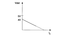
まず、外部制御ユニット93から高圧回路ユニット89に対して電流設定値を設定する。本例では、負荷電流検出回路83は図25に示すような電流電圧特性を持つように構成されているものとする。つまり、負荷電流が0の場合、4ボルト(V)でそこから負荷電流が流れるに伴って、小さい電圧値に直線的に変化していく。従って、電流設定を行う場合、4Vより小さい値を演算増幅器85の制御目標電圧値として設定することとなる。
【0037】
次に、出力オン/オフ信号をオンにする。すると、発振器78は所定の周波数、デューテイで発振を開始し、スイッチングトランジスタ79をスイッチング動作させる。そして、スイッチングトランジスタ79がオンの期間、入力電圧とオン時間及び高圧トランス74の入力インダクタンスに応じて所定のエネルギーが高圧トランス74に蓄積される。一方、スイッチングトランジスタ79がオフの期間には、そのエネルギーが高圧トランス74の入力インダクタンスと共振コンデンサ80とによってLC共振を起こし、スイッチングトランジスタ88のコレクタには、所謂フライバック電圧が発生する。この電圧は、巻数に応じて他の巻線にも伝達され、巻数の大きい出力巻線75aには高い電圧が発生する。これが整流ダイオード76を通じて外部負荷90に供給されることになる。一般的には、外部負荷90の容量92の成分により出力巻線のほぼピーク値Voがホールドされ、直流の高圧出力が外部負荷90に供給される。この時の外部負荷電流Idは、下記(1)式により求められる。
【0038】
Id=Vo/(R1+R2+R3)…(1)
ここで、R1は抵抗91の抵抗値、R2は抵抗82の抵抗値、R3は負荷電流検出回路83の合成インピーダンスをそれぞれ示す。
【0039】
この外部負荷電流により電流検出ポイントVdetの値は、その分下がる。この電流検出ポイントVdetの値が制御目標設定電圧86の値よりも大きい場合、演算増幅器85の出力電圧は上がり、高圧トランス74の入力電圧が上がる。これにより、高圧トランス74の出力電圧は上がり、負荷電流が増加し、電流検出ポイントVdetの値を小さくする方向へと動作する。逆に制御目標設定電圧86の値に対して電流検出ポイントVdetの値が低くなれば、演算増幅器85の出力電圧は下がり、高圧トランス74の入力電圧が下がる。
【0040】
以上により、負荷電流が設定した値と等しくなるように高圧トランス74の出力電圧が調整されることとなる。
【0041】
以上の例では高圧トランス74の入力電圧の大きさを増減することにより、高圧出力電流一定制御を実現するものであるが、高圧トランス74のスイッチング駆動におけるオンタイムの量を増減させ、高圧出力電流一定制御を実現するものもある。
【0042】
【発明が解決しようとする課題】
しかしながら、上記図18に示す従来例においては、以下のような問題点があった。
【0043】
(1)一次側のスイッチング素子4の駆動電流には二次側のフォワード巻線の出力電流が巻数比に逆比例して重畳されるため、24VUの平滑コンデンサの電圧が小さく、充電電流が大きい立ち上がり期間では一次側のスイッチング素子4に非常に大きな駆動電流を重畳してしまい、関係回路素子に負担をかける。
【0044】
(2)主たる制御の駆動源となる一次側LC電圧共振が安定な0ボルトスイッチによる発振状態に移行する以前から、上記状態が発生するため、安定な共振状態へ移行するまでの過渡期間が延び、より長い期間、関係回路素子に負担をかける。
【0045】
この様子を図20及び図21を用いて説明する。
【0046】
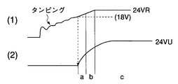
図20は、24VRと24VUの電圧立ち上がり波形を模式的に表わす図であり、同図の(1)24VRの電圧立ち上がり波形、(2)24VUの電圧立ち上がり波形、(3)は期間である。
【0047】
24VRは主制御部により主制御パルス(24VUスイッチング素子制御信号)19aのオン時間の緩やかな拡大、又は制御用比較基準値の緩やかな上昇等によるソフトスタート制御が機能し、所定時間をかけて最終目標値まで到達するように制御される。一方、24VUについては、その巻線元出力がフォワード側であるという性格上、24VRがソフトアップ中もほぼ最終値に近い波高値をもった出力が巻線より供給され、その結果、いち早く最終目標値に到達してしまう。
【0048】
図21は、図20のa,b,cのそれぞれの期間の24VU制御信号の波形、主制御信号(24VR制御信号)の波形、一次側スイッチング素子4の駆動電流の波形、コレクタ電圧の波形をそれぞれ示す図であり、同図の(1)は24VU制御信号の波形、(2)は主制御信号(24VR制御信号)の波形、(3)は一次側スイッチング素子4の駆動電流の波形、(4)はコレクタ電圧の波形である。
【0049】
期間aは24VRの立ち上がりの初期の様子を示している。主制御信号はソフトスタート機能により狭いオン期間をもったPWM信号でスタートしている。一方、24VUのの制御信号は24VUが目標値よりもずっと低いためにフォワード側オンの期間、完全オン状態となる(主制御信号とほぼ同一のPWM信号となる)。このとき、前述のように24VUのフォワード側巻線出力は既に最終値である。一次側の直流入力電圧の巻数比換算分(V24Uout)になっており、また、虹側出力コンデンサの充電電圧(24VU(t))が低いため、そのほとんどが平滑用インダクタンス(L24U)に印加され、大きな巻線出力電流(及びその大きな時間傾きα)を発生させることとなる。この二次側電流は巻数比に応じて一次側のスイッチング素子4の駆動電流となる。
【0050】
期間b,cと時間推移するごとに24VUの出力コンデンサの電圧は上昇し、当然、二次側の巻線出力電流は減少し、最終的には24VUの外部負荷がオンしない状態であればほぼ0となる。このとき、一次側電流は24VRのフライバックエネルギーを蓄積するためだけの駆動電流となる(高圧巻線の負荷電流は一般に極めて微小であるため無視してよい)。このときの一次側の電流増加の傾きは、ほぼ高圧トランス20の一次インダクタンスと直流入力電圧で決まる値となる。bにおいては、その中間状態にある期間となる。
【0051】
ここで、特にaの期間では、設計条件によっては一次側の駆動電流が、定常時(24VUの定格外部負荷電流が流れている状態)の最大値に比して、同等さらにはより大きくなってしまうことがあり、そのような場合には、一次側スイッチング素子4の駆動電流を検出して過電流保護をかけるような保護回路構成(図示省略)が実現できないか、又は保護レベルを定格負荷から期待されるものよりはるかに緩やかなものにせざるを得ない状況となる。
【0052】
以上は主に上記問題点(1)に関して述べたが、次に、上記問題点(2)に関して図22を用いて説明する。
【0053】
図22は、一次側のスイッチング素子4の駆動電流とコレクタ電圧の波形を起動時の3つの期間について模式的に示す図であり、同図の(1)は駆動電流の波形、(2)はコレクタ電圧の波形である。また、aは主制御パルスが出力開始した直後の期間を示す。共振コンデンサに一次巻線の他端に印加された直流電圧が完全充電された状態から主制御パルスがスタートする。パルス幅は最も細い状態から開始するように制御される(ソフトスタート)が、共振コンデンサの充電負荷をスイッチング素子4がショートする形となるため、この期間、図示のように時間的には短いが非常に大きい電流が流れる。この期間は当然、LC共振を発生させるための十分なトランス駆動電流が流れておらず、フライバック波形が0ボルトまでは全く跳ね返ることができない。
【0054】
その後、期間cのような完全な0ボルトスイッチによる電圧共振波形が得られるようになる前に、期間bのようにフライバック波形が徐々に成長しつつも、依然としてフライバックエネルギーが低く、正常な0ボルトスイッチが実現できない過渡期間を送る。この期間に24VUの充電電流が重畳されると、同図の上側のような一次側電流波形となり、共振コンデンサの残電圧をスイッチング素子4がショートする電流と二次側からの重畳電流が合わされ、大きな電流負荷をスイッチング素子4にかけることとなる。
【0055】
他、主たる制御は、上述したように一次側の駆動電流が正から負に切り換わった瞬間を検出して、次のオン動作を開始するような制御アルゴルの場合、24VUの充電電流が正の方向として一次側に重畳される過渡期間には、フライバック共振波形が0ボルトまで振れ込むことを、より一層阻害する形となり、正常な0ボルトスイッチによる電圧共振制御状態への移行が一層遅れてしまうこととなる。
【0056】
また、上記図23に示す従来例においては、定電流出力iには出力電圧が小さく、負荷の抵抗分流れる電流に対して容量成分を充電する電流が総負荷電流の大部分を占める期間は、出力電圧はほぼ下記(2)式
(i×t)/c…(2)
となり、定電流値に比例した傾きをもって時間と共に直線状に増加していく波形となる。また、並列にある抵抗成分rも含めて考えた場合は、最終出力に対する時間変化はcrを時定数とした{1−exp(−t/cr)}で表わされる。その際、出力負荷の抵抗成分、容量成分の値によっては最終出力値に到達するのにかなりの時間を要する場合がある。例えば、付加容量を200pf、負荷抵抗を500MΩとした場合、cr時定数は、100ms程度となり、最終値に対して更に近い割合の出力を得るためには当然それ以上の時間を要することとなる。
【0057】
先に、負荷インピーダンスの測定は画像形成期間以外において実施すると述べたが、例えば、画像形成期間の前に負荷インピーダンスの測定を行う場合、複写動作の前処理シーケンスによっては、所謂ファーストコピータイムに負荷インピーダンス測定期間をそのまま追加して考慮しなければならない場合も考えられ、ユーザーに対してファーストコピーの速さを商品価値としてアピールするような装置の場合には、その様なレベルの処理時間も無視することができず、より速やかな測定方法が求められることとなる。
【0058】
更に、図24に示す従来例においては、外部負荷回路の抵抗値が何等かの原因で非常に高抵抗となった場合、例えば、高圧電源ユニットの出力から外部負荷への給電経路に不良が発生した場合や、何等かの目的で接続ケーブルが外された場合等には、負荷電流が流れないために、定電流制御ループが回路ユニットの持つ最大能力まで高圧トランスの入力電圧を上昇させる、もしくはオンタイムを増加させることになり、通常の負荷において求められる最高出力を大きく越えて出力してしまうこととなる。
【0059】
本発明は上記従来技術の有する問題点を解消するためになされたもので、その第1の目的とするところは、可能な限り迅速に負荷への出力を定常状態にすることができる電源回路を提供することである。
【0060】
また、本発明の第2の目的とするところは、負荷に印加される電圧が過大になることを防止することができる電源回路を提供することである。
【0061】
また、本発明の第3の目的とするところは、トランスの一時側に大きな電流が流れてしまうことを防止することができる電源回路を提供することである。
【0062】
【課題を解決するための手段】
上記第1の目的を達成するために本発明の請求項1記載の電源回路は、負荷電流を検出する負荷電流検出手段と、該負荷電流検出手段からの出力に応じて変圧器の入力電圧または駆動PWM(パルス幅変調)のオン時間もしくはオンデューティを制御して前記負荷電流が所定値となるように出力電圧を制御する出力電圧制御手段とを有する電源回路において、前記出力電圧制御手段による定電流制御の開始後所定期間は目標出力電流制御値より大きい出力電流制御値を設定する出力電流制御値設定手段と、前記出力電流制御値設定手段により設定された出力電流制御値での制御開始から一定時間後に設定された前記出力電流制御値を前記目標出力電流値に再設定する出力電流制御値再設定手段とを具備したことを特徴とするものである。
【0065】
また、上記第1の目的を達成するために本発明の請求項2記載の電源回路は、負荷電流を検出する負荷電流検出手段と、該負荷電流検出手段からの出力に応じて変圧器の入力電圧または駆動PWM(パルス幅変調)のオン時間もしくはオンデューティを制御して前記負荷電流が所定値となるように出力電圧を制御する定電流制御手段と、前記出力電圧を検出する出力電圧検出手段と、前記出力電圧検出手段からの出力に基づいて前記変圧器の入力電圧または駆動PWMのオン時間もしくはオンデューティを制御して出力電圧が所定値となるように制御する出力電圧制御手段とを有する電源回路において、前記出力電圧制御手段の起動/停止を制御する起動/停止制御手段と、所定の出力電流制御値を設定する出力電流制御値設定手段とを具備し、所望の電圧が得られるように初めに前記起動/停止制御手段により前記出力電圧制御手段を起動させ、前記出力電圧検出手段により検出される電圧が前記所望の電圧に到達した後、前記起動/停止制御手段により前記出力電圧制御手段の動作を停止させると共に、出力電流制御値設定手段により目標出力電流制御値を設定し、前記定電流制御手段により定電流制御を開始することを特徴とするものである。
【0067】
また、上記第2の目的を達成するために本発明の請求項3記載の電源回路は、負荷電流を検出する負荷電流検出手段と、該負荷電流検出手段からの出力に応じて変圧器の入力電圧または駆動PWM(パルス幅変調)のオン時間もしくはオンデューティを制御して前記負荷電流が所定値となるように出力電圧を制御する出力電圧制御手段と、前記負荷電流を検出する負荷電流検出手段とを有する電源回路において、前記出力電圧制御手段の定電流制御動作が開始して所定時間経過後も前記負荷電流検出手段の検出値が所定値以下である場合、前記出力電圧制御手段の動作を停止または中断するように制御する出力動作制御手段を具備したことを特徴とするものである。
【0068】
また、上記第2の目的を達成するために本発明の請求項4記載の電源回路は、請求項3記載の電源回路において、前記出力電圧制御手段の定電流制御動作が開始して所定時間経過後も前記負荷電流検出手段の検出値が所定値以下である場合、その旨を電源回路の動作を指示する外部装置に通知する通知手段を具備したことを特徴とするものである。
【0070】
また、上記第3の目的を達成するために本発明の請求項5記載の電源回路は、一端を所定の直流電圧入力とし且つ他端を所定状態にオン/オフ動作させる一次巻線と前記一次巻線のオフ時にエネルギーを取り出す少なくとも1つフライバック巻線と前記一次巻線のオン時にエネルギーを取り出す少なくとも1つのフォワード巻線と前記一次巻線のオフ時及びオン時の全周期に亘ってエネルギーを取り出す高圧出力巻線とを含むトランスと、前記フライバック巻線の整流出力電圧を検出する電圧検出手段と、該電圧検出手段の検出結果により前記一次巻線のオン動作時間を制御し且つ前記フライバック巻線の整流出力電圧を所定値に制御する主制御手段と、前記フォワード巻線の出力の整流平滑電圧を比較用基準電圧と比較し、前記フォワード巻線に設けられたスイッチング素子を制御することにより前記整流平滑電圧を目標値に制御する副制御手段とを有する電源回路において、前記副制御手段は、前記主制御手段の起動時に前記フライバック巻線の整流出力電圧が所定値を超えるまで前記フォワード巻線の出力の1サイクル中の導通時間を所定値以下に抑制することにより、前記主制御手段が正常な制御状態になった後に前記フォワード巻線の出力の整流平滑電圧をオン / オフ制御可能とするように制御することを特徴とするものである。
【0071】
また、上記第3の目的を達成するために本発明の請求項6記載の電源回路は、請求項5記載の電源回路において、前記副制御手段は、前記主制御手段の起動時に前記フライバック巻線の整流出力電圧が所定値を超えると前記比較用基準電圧を徐々に増加させることを特徴とするものである。
【0072】
また、上記第3の目的を達成するために本発明の請求項7記載の電源回路は、請求項5記載の電源回路において、前記副制御手段は、前記フォワード巻線の出力の整流平滑電圧と比較用基準電圧との比較出力を所定のパターン信号と比較する比較手段を有し、前記主制御手段の起動時に前記フライバック巻線の整流出力電圧が所定値を超えるまで、前記フォワード巻線の出力の整流平滑電圧と比較用基準電圧との比較出力を制限することを特徴とするものである。
【0075】
【発明の実施の形態】
以下、本発明の各実施の形態を図1〜図17に基づき説明する。
【0076】
(第1の実施の形態)
まず、本発明の第1の実施の形態を図1〜図3に基づき説明する。尚、本実施の形態に係る電源回路の定電圧制御回路を除く基本的な構成は、上述した従来の図18に示す構成と同一であるから、同図を流用して説明する。
【0077】
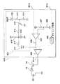
図1は、本発明の第1の実施の形態に係る電源回路における定電圧制御回路の構成を示すブロック図であり、同図中、101は定電圧制御回路で、制御用比較電圧生成回路102、比較器103、フィルター回路104を有している。
【0078】
制御用比較電圧生成回路102は、ツェナーダイオード105、トランジスタ106,107、基準電圧発生素子108、コンデンサ109,110、抵抗111,112,113,114,115を有している。尚、101aは24VU用スイッチング素子14の駆動信号出力部、101bは24VU平滑出力検出信号入力部である。
【0079】
ツェナーダイオード105は、24VRの電圧を検出するための素子で、本実施の形態ではオン電圧を16ボルト(V)とする。電源起動時、主制御対象であるフライバック出力(以下、24VRと称する)が16Vを越えたところで、ツェナーダイオード105がオンし、後段のトランジスタ106,107をオンさせる。この結果、基準電圧発生素子108に電圧が供給され、24VUの定電圧制御用比較電圧116が後段の比較器103に送られ、また、この比較器103には24VU平滑出力検出入力部101bを介して24VU平滑出力検出信号が送られる。そして、この比較器103により24VUの定電圧制御用比較電圧116と24VU平滑出力検出信号とが比較される。ここで、比較電圧116の出力部には所定の時定数回路が構成されており、所定の傾きを持ってソフトアップすることとなる。
【0080】
この様子を図2に示し、同図の(1)は24VRの出力、(2)は24VUの出力を示す。上述したように24VUの比較電圧値がソフトアップするため、24VUの出力電圧値も定電圧制御によって同型のソフトアップとなる。図2中、a,b,cの各期間の主制御ループのPWM信号、24VUの導通制御信号(24VU用スイッチング素子14の駆動信号)及び一次側スイッチング素子4の駆動電流の出力タイミングを図3に示す。同図の(1)は24VUの導通制御信号、(2)は主制御ループのPWM信号、(3)は一次側スイッチング素子の駆動電流である。
【0081】
24VRを制御するための主制御信号MPWMは期間a,b,cと時間推移するのに伴って目標電圧値がソフトアップされるため徐々にオンデューティが増加していく。一方、24VUの導通制御信号は上述したように24VRが16Vを越えたところから制御電圧値がソフトアップするという違いはあるが、やはり期間a,b,cと時間推移するのに伴って徐々にオンデューティが増加していく。これにより、24VUの出力電圧が低く、24VUの巻線出力電流及びその時間上昇率が大きくなる期間aでも、24VUの導通制御素子であるスイッチング素子14のオン期間は短く絞られているために、一次側の最大ピーク電流は所定値以下に押さえられる。図3において、一次側スイッチング素子4の駆動電流に2つの傾きがあるのは、24VRのフライバックエネルギー用の駆動信号のみ流れている期間と、24VUの導通制御素子であるスイッチング素子14がオンし、24VUの出力平滑コンデンサ17への充電電流分が重畳される期間があるためである。24VUの出力平滑コンデンサ17への充電電流の傾きは、24VUの電圧が大きくなるのに伴って小さくなり、最終的にはほぼ0となるため(24VUの外部負荷9がオンしていない期間内の説明であり、もちろん、外部負荷9がオンすれば、その電流分が重畳される)、24VRの駆動電流のみとなる。
【0082】
以上のように、本実施の形態に係る電源回路によれば、24VUの制御用比較電圧値を、24VRを監視して所定値以上になったところからソフトアップスタートするようにすることで、常に主制御ループが正常な制御状態に入ったところからフォワード巻線23の制御を開始することができ、また、フォワード巻線23の起動時の大きな充電電流値をソフトアップすることができ、一次側駆動電流の電流負荷を軽減することができる。
【0083】
(第2の実施の形態)
次に、本発明の第2の実施の形態を図4及び図5に基づき説明する。尚、本実施の形態に係る電源回路の定電圧制御回路を除く基本的な構成は、上述した従来の図18に示す構成と同一であるから、同図を流用して説明する。
【0084】
上述した第1の実施の形態では24VUの制御用比較電圧をソフトアップさせることが特徴の1つであったが、本実施の形態では、目標電圧値と検出電圧値との比較結果に対して、所定の条件下で二次側フォワード巻線32の最大導通期間を制限できるようにしたことを特徴とするものである。
【0085】
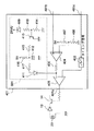
図4は、本発明の第2の実施の形態に係る電源回路における定電圧制御回路の構成を示すブロック図であり、同図において、401は定電圧制御回路で、スライスレベルの制限回路402、三角波生成回路403、比較器404,405、抵抗406,407,408を有している。尚、401aは24VU用スイッチング素子14の駆動信号出力部、401bは24VU平滑出力検出信号入力部、401cはスイッチング素子4の駆動信号入力部である。
【0086】
三角波生成回路403は、スイッチング素子4の駆動信号入力部401cから入力する一次側フライバック波形のゼロクロスタイミング信号を基準にして図5に示すような位相で三角波を生成する。図5の(1)はトランスの一次側の信号、(2)はスイッチング素子4のベースに入る駆動信号、(3)は三角波生成回路403により生成された三角波、(4)は24VU用スイッチング素子14の駆動信号出力部401aから出力する駆動信号である。
【0087】
比較器404は、比較電圧と24VU平滑出力検出信号入力部401bを介して入力する検出電圧とを比較する。比較器405は、三角波生成回路403の出力と比較器404の出力とを比較し、24VU巻線の導通制御用PWM信号(24VU用スイッチング素子14の駆動信号)を生成する。定常状態においては、比較器404の出力は、所定のアナログレベルに安定し、三角波をスライスし、24VU巻線の導通制御用PWM信号を発生させる。
【0088】
次に、本実施の形態の特徴である制限回路402がどのように機能するかを説明する。
【0089】
制限回路402は、ツェナーダイオード409、トランジスタ410、ダイオード411、コンデンサ412、抵抗413,414,415,416,417を有している。ツェナーダイオード409は、24VRの電圧をモニターするための素子で、本実施の形態では16Vとする。24VRが16V以下のレベルではトランジスタ410はオフとなり、時定数回路のコンデンサ412には5Vの電圧が充電されている。この状態では、24VUの電圧が立ち上がる前で、比較電圧と検出電圧との比較結果がLに張り付いた状態であっても比較器404の出力抵抗406と時定数回路の出力抵抗416及びダイオード411の順電圧のバランスにより、24VUの巻線出力の導通期間を0もしくは所定値以下になるようにスライスレベルを強制的に規定するような機能を実現する。
【0090】
この様子を表わす図が図5であり、比較器404のみの上述した第1の実施の形態の場合のスライスレベルがbであり、本実施の形態をの場合のスライスレベルがaである。
【0091】
ここで、24VRが起動し、16Vを超えたところでトランジスタ410がオンし、時定数回路の出力レベルを漸次下げていく比較器404からの出力電圧以下となったところで、制限回路402の動作は終了する。時定数回路は24VUの立ち上がり速度を考慮にいれ、適切な時定数を設定する。
【0092】
以上により、上述した第1の実施の形態の図3と同様に、24VRの起動状態と連係し、フォワード巻線23の導通角が所定のソフトアップを行うようにすることができる。
【0093】
(第3の実施の形態)
次に、本発明の第3の実施の形態を図6に基づき説明する。尚、本実施の形態に係る電源回路の定電圧制御回路を除く基本的な構成は、上述した従来の図18に示す構成と同一であるから、同図を流用して説明する。
【0094】
本実施例の特徴は、スライスレベルの制限回路において監視する電圧を24VU自身にしたことである。
【0095】
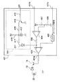
図6は、本発明の第3の実施の形態に係る電源回路における定電圧制御回路の構成を示すブロック図であり、同図において、上述した第2の実施の形態における図4と同一構成部分には同一符号が付してある。図6において図4と異なる点は、制限回路の構成である。即ち、本実施の形態における制限回路601は、監視する電圧を24VU自身にしたことにより、24VUが所定値以下の場合はスライスレベルを強制的にシフトさせ、24VU巻線の導通角を起動時には所定の時間に制限することができる。
【0096】
本実施の形態の場合は、第2の実施の形態の場合に比べて時定数回路の時定数設計が容易であるという利点がある。つまり、本実施の形態では24VUの立ち上がり時間によらず、24VU自身が所定値まで上昇するまでは強制的に24VU巻線の導通角を所定値以下に制限するため、電源ユニットへの入力電圧(例えば、商用AC電源電圧)の大きさ、24VUの外部負荷の容量の大きさ、また、起動中にも外部負荷がオンする場合には、その負荷電流値の大きさ等の差による実際の24VUの立ち上がり速度差を考慮に入れる必要がなくなる。
【0097】
(第4の実施の形態)
次に、本発明の第4の実施の形態を図7に基づき説明する。尚、本実施の形態に係る電源回路の定電圧制御回路を除く基本的な構成は、上述した従来の図18に示す構成と同一であるから、同図を流用して説明する。
【0098】
本実施例の特徴は、スライスレベルの制限回路において、スライスレベル制限機能のオン/オフを主制御部9から入力するようにしたことである。
【0099】
図7は、本発明の第4の実施の形態に係る電源回路における出力制限回路の構成を示すブロック図であり、同図において、上述した第3の実施の形態における図6と同一構成部分には同一符号が付してある。本実施の形態における制限回路701は、図6の制限回路601の構成からツェナーダイオード409及び抵抗414を削除したもので、スライスレベル制限機能のオン/オフが主制御部9から入力される。主制御部9は、24VRの制御を行っており、24VRの制御状態(オン、オフ、起動中等)認識できるので、例えば、24VRが所定の電圧になった後、所定時間経過後、制限回路701の機能を抑制する等の処理が可能である。
【0100】
(第5の実施の形態)
次に、本発明の第5の実施の形態を図8〜図10に基づき説明する。
【0101】
図8は、本発明の第5の実施の形態に係る電源回路の構成を示すブロック図である。同図において、上述した従来の図23と同一構成部分には同一符号が付してある。図8において、図23と異なる点は、図23の構成に定電流設定値切換回路801を付加し、定電流制御回路の電流設定値を定電流設定値切換回路801を通して、電源コントローラ67より2段階に設定可能としたことである。定電流設定値切換回路801は、トランジスタ802、抵抗803,804,805を有している。
【0102】
次に、本実施の形態に係る電源回路の動作を図8、図9及び図10を用いて説明する。図9は、本実施の形態に係る電源回路の動作制御手順を示すフローチャート、図10は、本実施の形態に係る電源回路の動作概要を示すための出力電圧の時間変化を示す曲線図である。図10の例では、定電流制御回路による負荷容量に対する充電速度を主たる議論の中心とするために、電圧立ち上がり波形は、起動後の適当期間を直線的に表わし、その後、expに近い曲線で近似したもので考える。
【0103】
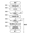
まず、外部コントローラより負荷抵抗測定開始命令を受け取る。すると、定電流制御回路の電流設定値を最終目標電流I1よりも2倍大きいI0に設定する(ステップS901)。本実施の形態では電源コントローラ67が定電流設定値切換回路801のトランジスタ802をオンする信号を出力することに対応する。その後、発振回路38に対してオン信号を出力し、高圧出力を開始する(ステップS902)。このとき、出力電圧は図10のaのように、最終目標I1でスタートさせた場合の立ち上がりbより2倍の傾きで出力電圧を上昇させる。
【0104】
次いでステップS903で電源コントローラ67では、出力開始後の経過時間を計測し、その計測結果に基づいて予め決められた時間t1が経過したか否かを経過するまで判断する(ステップS903)。そして、予め決められた時間t1が経過したところで、定電流設定値をI1に切り換え設定する(ステップS904)。最終的な出力電圧は、最終的な出力定電流値と負荷の抵抗成分の変動が通常ある範囲内の中で変動すると考えて良く、本実施の形態では図10のVaからVbまでと想定する。
【0105】
今、最終出力電圧がVaとなるような負荷を考えると、切り換えたときの出力電圧値Vchからは電圧の傾きが1/2程度に落ちて上昇が始まり、ゆっくりと曲線を描きつつ、最終値に到達していく。そして、出力開始後の経過時間計測結果に基づいて予め決められた時間t2が経過したか否かを経過するまで判断する(ステップS905)。そして、予め決められた時間t2が経過したところで、検出巻線出力が取り込まれ(ステップS906)、画像域最高定電圧値が計算された後、本処理動作を終了する。これにより、ほぼ負荷容量は完全に充電され、出力電圧は、ほぼ一定となる。
【0106】
初めの定電流値をI0とした場合とI1とした場合とでVchを得るために必要な期間は、約2倍程度の差が生じるため、最終電圧値を得るための時間は、本実施の形態においては、概ねt1程度短縮することが可能となる。
【0107】
最終出力がVbとなるような負荷の場合には、切り換え後に図10のcのような直線になり、このときは電圧変化の時定数に高圧トランス30内部のブリーダ抵抗の放電部分が加味されて、より速い応答となり、すばやく最終値に到達する。
【0108】
(第6の実施の形態)
次に、本発明の第6の実施の形態を図11及び図12に基づき説明する。尚、本実施の形態に係る電源回路の基本的な構成は、上述した第5の実施の形態の図8と同一であるから、同図を流用して説明する。
【0109】
図11は、本実施の形態に係る電源回路の動作制御手順を示すフローチャート、図12は、本実施の形態に係る電源回路の動作概要を示すための出力電圧の時間変化を示す曲線図である。
【0110】
まず、外部コントローラより負荷抵抗測定開始命令を受け取る。すると、図11において、まず、電源回路は定電圧値をVbに設定し(ステップS1101)、出力電圧をVb一定とするような定電圧制御モードによる制御を開始する。その後、発振回路38に対してオン信号を出力し(ステップS1102)、出力電圧Vbに対応した検出巻線電圧が得られるように、逐次検出巻線出力を取り込み(ステップS1103)、整流平滑回路68を通してA/D入力し、出力電圧がVbになったか否かを、Vbになるまで判断する(ステップS1104)。その判断結果に基づいて定電圧制御回路52からの出力電圧のレベルを出力ポートのオン/オフ率を切り換えることにより実現する。子のとき、回路動作は、負荷電流に無関係に、目標電圧値に向かって電源回路がもつ最大の出力能力で出力電圧を上昇させていくと考えて良い。そして、出力電圧がVbなったところで、定電流設定値をI1に切り換え設定し(ステップS1105)、電源回路を定電流モードに切り換えるべく、定電圧制御回路52の出力をオフ(0ボルト)とする。すると、Vbから目的の定電流値を得るべく定電流制御ループが機能し、上述した第5の実施の形態における図9のステップS905〜ステップS907までと同様の後処理を行う(ステップS1106)。
【0111】
本実施の形態に係る電源回路によれば、Vbまでは電源回路がもつ最大出力能力により、出力電圧を上昇させるため、切り換え前の電圧上昇を最速とすることができる。Vbとしては通常の負荷変動域のうち最も低い抵抗値に対して、所望の定電流をかけた電圧を設定することによって、過渡的な電圧オーバーシュートを非常に小さくできる。
【0112】
(第7の実施の形態)
次に、本発明の第7の実施の形態を図13及び図14に基づき説明する。図13は、本発明の第7の実施の形態に係る電源回路における出力制限回路の構成を示すブロック図である。
【0113】
図13において、1301は外部制御ユニットから電源回路内に高圧の出力オン/オフを指令する外部信号で、本図ではEX−ON*と表わし、H(ハイレベル)で出力オフ、L(ローレベル)で出力オンを命令するものと論理規定する。1302はEX−ON*信号を受けて、高圧回路の動作を実際にオン/オフさせる内部信号で、IN−ON*と表わし、H(ハイレベル)で出力オフ、L(ローレベル)で出力オンを命令するものと論理規定する。1303は第1タイマーで、EX−ON*がLとなったことを受け、IN−ON*がLになった時刻から所定の時間、内部オン*をLにさせるために時間を計測する。この第1タイマー1303は、トランジスタ1303a、1303b、1303c、コンデンサ1303d、1303e、抵抗1303f、1303gを有している。
【0114】
また、図13において、1304は第2のタイマーで、第1タイマー1303により所定時間、IN−ON*がLになった後、負荷電流検出手段から負荷電流が所定値しか流れていないことを検知した際に、所定の時間IN−ON*をHにさせるものである。この第2のタイマー1304は、トランジスタ1304a、1304b、1304c、コンデンサ1304d、1304e、抵抗1304f、1304g、1304hを有している。
【0115】
また、図13において、1305は第1タイマー1303をスタートさせる信号(T1−S)、1306は第1タイマー1303の計測結果信号(T1−Q)、1307は第2タイマー1304をスタートさせる信号(T2−S)、1308は第2タイマー1304の計測結果信号(T2−Q)、1309は第1タイマー1303及び第2タイマー1304の時間計測動作をリセットさせる信号(RESET)、1310は負荷電流検出手段からの出力信号(Vdet)で、本実施の形態では上述した従来例の図24に示したような電圧−電流特性を持つものを想定する。1311は負荷電流が所定値以下か、以上かを判別するための電圧判別手段で、本実施の形態では2.4Vにてオンするツェナーダイオードである。
【0116】
また、図13において、1312、1313、1314、1315はトランジスタ、1316、1317はダイオード、1318、1319、1320は抵抗である。
【0117】
図14は、図13における各信号の出力タイミングを示すタイムチャートである。同図の(a)はEX−ON*、(b)はT1−S(IN−ON*)、(c)はT1−Q、(d)はT2−S、(e)はT2−Q、(f)はVdetをそれぞれ示す。
【0118】
次に、上記構成の電源回路における出力制限回路の動作を、図13及び図14を用いて説明する。
【0119】
まず、外部制御信号EX−ON*がHで、高圧出力オフの定常状態を考える。EX−ON*=Hのため、RESET=Hとなり、第1タイマー1303及び第2タイマー1304は共にリセット状態となり、T1−Q、T2−Qは共にオープン状態となる。IN−ON*はもちろんHとなり、高圧出力はオフ状態となる。
【0120】
次に、負荷電流値が設定され(図14のタイムチャートには図示せず)、その後、EX−ON*がLになった場合を考える。EX−ON*=Lになったことを受け、両タイマー1303,1304へのRESETはLとなり、リセット状態は解放される。そして、IN−ON*=Lとなり、高圧出力回路が所定の負荷電流が得られるまで出力電圧を上昇させる動作を開始する。これと同時にT1−SはLになり、これをトリガーに第1タイマー1303がIN−ON*=Lの時間計測を開始する。
【0121】
第1タイマー1303がタイムアップするとT1−Q=Lとなり、このとき、もし負荷電流が所定値以上流れていない場合(本実施の形態ではVdetが約3V以下になっていない場合)、これを受けて電圧検出手段が1311が導通し、2段のトランジスタ1314,1315をオンさせる。これを受けてIN−ON*の前段のトランジスタ1313のベース入力をダイオード1317を介してLにし、IN−ON*を強制的にHに戻し、高圧出力動作を中断させる。また、これと同時に第2タイマー1304のT2−SがLになり、高圧出力を中断させる時間の計測を開始させる。
【0122】
第2タイマー1304がタイムアップするとT2−QがLになり、IN−ON*を再びLにし、高圧出力をオンさせると共に、T1−SがLになり、これをトリガーに第1タイマー1303がIN−ON*=Lの時間計測を開始する。負荷ケーブルが抜かれる等、何等かの理由で負荷抵抗が所定値以上の値になっている状態では、外部制御信号EX−ON*がLである間、以上の動作を繰り返すこととなる。通常の負荷が正常に接続された場合、負荷電流検出手段からの出力が所定値以下となり、電圧判別手段1311がオフとなり、高圧出力動作の中断シーケンスは回避される。また、外部制御信号EX−ON*がHとなった場合には初期状態に戻り、高圧出力オフとなる。
【0123】
以上のように、本実施の形態に係る電源回路によって、負荷ケーブルの引き抜き等により負荷抵抗の値が通常の値に比して非常に大きくなった場合には、出力動作を電源回路内で独立に間欠動作とすることができる。
【0124】
(第8の実施の形態)
次に、本発明の第8の実施の形態を図15及び図16に基づき説明する。本実施の形態に係る電源回路は、他の機能ブロック、例えば低圧電源回路、蛍光灯インバータ回路、ヒータ制御回路等を含み、それらの複雑なシーケンス制御を行う必要がある場合等に適用される。
【0125】
図15は、本発明の第8の実施の形態に係る電源回路の構成を示すブロック図であり、同図において、1501は電源回路で、電源制御用マイクロコンピュータ(以下、電源コントローラと称する)1502、高圧生成ブロック1503を有している。電源コントローラ1502は、電源回路1501全体の制御を行う。高圧生成ブロック1503は、電源コントローラ1502のD/Aポートから出力される出力負荷電流設定信号(情報)1504及び内部出力オン信号(IN−ON*)1505を受け、高圧生成動作を行う。高圧生成ブロック1503から電源コントローラ1502のA/Dポートに負荷電流検出手段からの出力電圧Vdetが取り込まれる。また、電源コントローラ1502には外部制御ユニット1507が接続され、該外部制御ユニット1507から電源コントローラ1502に負荷電流の設定情報1508や出力オン信号(EX−ON*)/出力オフ信号1509が送られる。
【0126】
次に、本実施の形態に係る電源回路における電源コントローラ1502の動作を、図16のフローチャートに基づき説明する。
【0127】
まず、外部制御ユニット1507から通信により(プロトコルその他の詳細構成は各種考えられるので、ここではとくに言及しない)、電源コントローラ1502に対して負荷電流の設定信号1504及び内部出力オン信号(IN−ON*)1505が伝えられる。これを受けて高圧生成ブロック1503に対して電源コントローラ1502のD/Aポートから対応する負荷電流制御用目標電圧1504が設定される(ステップS1601及びステップS1602)。
【0128】
本実施の形態では、「D/Aポートより」と記述したが、例えば、所定の周波数及びデューティを持つPWM(パルス幅変調)信号を出力ポートより出力し、これをローパスフィルタに通し、アナログ電圧を得ること等の方法も考えられる。
【0129】
次に、高圧生成ブロック1503に対して出力動作のオンを伝える内部出力オン信号(IN−ON*)=Lが出力される(ステップS1603)。以上により高圧生成ブロック1503は負荷電流が所定値となるべく、出力電圧を上昇させる。その後、電源コントローラ1502内での時間管理によって、所定時間が経過したか否かを経過するまで判別する(ステップS1604)。後、負荷電流検出手段からの出力電圧Vdetを電源コントローラ1502のA/Dポートより取り込み、負荷電流Idが所定値ID以上になっているか否か判別する(ステップS1605)。そして、負荷電流Id>IDの場合は、出力オフ信号を外部制御ユニット1507から受信したか否かを判別し(、受信した場合には、内部出力オン信号(IN−ON*)をオフとして高圧出力動作を終了する。また、出力オフ信号を外部制御ユニット1507から受信しない場合には、再び所定時間経過後、負荷電流の判別を行うために、先のステップS1603における内部出力オン信号(IN−ON*)=オンのシーケンスに戻る。
【0130】
一方、前記負荷電流Id<IDの場合は、内部出力オン信号(IN−ON*)を所定時間の間一旦オフした後(ステップS1608)、同様に外部制御ユニット1507から出力オフ信号を受信したか否かの判別シーンスに入り、電源コントローラ1502内での時間管理によって、所定時間が経過したか否かを経過するまで判別する(ステップS1609)。その後、同様に外部制御ユニット1507から出力オフ命令信号を受信したか否かの判別シーケンスに入り、上記と同様な手順を踏むものである。
【0162】
(第9の実施の形態)
次に、本発明の第9の実施の形態を図17に基づき説明する。図17は、本発明の第9の実施の形態に係る電源回路の構成を示すブロック図であり、同図において、1701は電源回路で、トランジスタ1702、ツェナーダイオード1703、抵抗1704,1705,1706,1707,1708,1709、コンデンサ1710,1711を有している。そして、外部制御ユニット1712から電流設定PWM(パルス幅変調)信号1713、及び外部オン信号(EX−ON*)1714が電源回路1701に入力される。また、電源回路1701から電流オン/オフ検知信号1715が入力される。
【0163】
本実施の形態に係る電源回路1701は、電源回路1701側に上述した第8の実施の形態で述べたような電源コントローラを具備しないような構成の場合に効果的である。
【0164】
次に、本実施の形態に係る電源回路1701の動作を説明する。
【0165】
まず、外部制御ユニット1712より電源コントローラに対して負荷電流の設定情報が伝えられる。本実施の形態では、電源回路1701に対して所定の周波数及びデューティを持つPWM(パルス幅変調)信号を外部制御ユニット1712の出力ポートから出力し、これをローパスフィルタを用いてフィルタリングしてアナログ電圧を得る構成例を示している。次に、出力動作のオンを伝えるEX−ON*=Lが出力される。以上によって、電源回路は負荷電流が所定値となるべく出力電圧を上昇させる。
【0166】
その後、外部制御ユニット1712での時間管理によって、所定時間が経過した後、負荷電流検出手段からの出力を読み込み、負荷電流IDが所定値ID以上になっているか否かを判別する。
【0167】
Id<IDの場合、EX−ON*をHとして高圧出力動作を一旦中断させる。その後、必要に応じて同じ手順で出力命令を出し、所定時間経過後、負荷電流をチェックするシーケンスを繰り返す。更に、必要であれば、最大繰り返し回数を設定し、所定回数、再出力命令を発行しても負荷電流が所定値以上を示さない場合は、高圧負荷以上として、装置としてのエラー処理に移行する等の処置も外部制御ユニット1712のシーケンス構成により可能である。また、Id>IDの場合は、出力中断手順をスキップする。
【0168】
以上のように本実施の形態に係る電源回路1701によれば、電源回路1701にマイクロコンピュータ等の電源コントローラが具備されていない場合にも、負荷電流値の判別結果のみをシーケンス制御手段を利用し、出力動作を間欠動作させるか、または出力動作を強制的に終了させ、装置としてのエラーシーケンス々移行する等の高度の保護処理が可能である。
【0169】
【発明の効果】
以上詳述したように本発明の請求項1及び2に記載の電源回路によれば、可能な限り迅速に負荷への出力を定常状態にすることができる。
【0170】
また、本発明の請求項3及び4に記載の電源回路によれば、負荷に印加される電圧が過大になることを防止することができる。
【0171】
更に、本発明の請求項5乃至7に記載の電源回路によれば、トランスの一時側に大きな電流が流れてしまうことを防止することができる。
【図面の簡単な説明】
【図1】本発明の第1の実施の形態に係る電源回路における定電圧制御回路の構成を示すブロック図である。
【図2】同実施の形態に係る電源回路における信号出力状態を示す図である。
【図3】同実施の形態に係る電源回路における各信号及び駆動電流の出力タイミングを示す図である。
【図4】本発明の第2の実施の形態に係る電源回路における定電圧制御回路の構成を示すブロック図である。
【図5】図4に示す定電圧制御回路における各信号波形を示す図である。
【図6】本発明の第3の実施の形態に係る電源回路における定電圧制御回路の構成を示すブロック図である。
【図7】本発明の第4の実施の形態に係る電源回路における出力制限回路の構成を示すブロック図である。
【図8】本発明の第5の実施の形態に係る電源回路の構成を示すブロック図である。
【図9】同実施の形態に係る電源回路の動作制御手順を示すフローチャートである。
【図10】同実施の形態に係る電源回路の動作概要を示す図である。
【図11】本発明の第6の実施の形態に係る電源回路の動作制御手順を示すフローチャートである。
【図12】同実施の形態に係る電源回路の動作概要を示す図である。
【図13】本発明の第7の実施の形態に係る電源回路における出力制限回路の構成を示すブロック図である。
【図14】同実施の形態に係る電源回路における各信号の出力タイミングを示す図である。
【図15】本発明の第8の実施の形態に係る電源回路の構成を示すブロック図である。
【図16】同実施の形態に係る電源回路の動作制御手順を示すフローチャートである。
【図17】本発明の第9の実施の形態に係る電源回路の構成を示すブロック図である。
【図18】従来の電源回路の構成を示すブロック図である。
【図19】図18に示す従来の電源回路における定常時の主要な動作波形を示す図である。
【図20】図18に示す従来の電源回路における電圧立ち上がり波形を示す図である。
【図21】図20のa〜cの各期間における各信号波形を示す図である。
【図22】図18に示す従来の電源回路における一次側スイッチング素子の波形を示す図である。
【図23】図18と異なる従来の電源回路の構成を示すブロック図である。
【図24】図18及び図23と異なる従来の電源回路の構成を示すブロック図である。
【図25】図24に示す従来の電源回路における負荷検出回路の電流電圧特性を示す図である。
【符号の説明】
1 商用AC電源
2 整流ブリッジ
3 第1の平滑コンデンサ
4 第1のスイッチング素子
5 共振コンデンサ
6 クランプダイオード
7 カレントランス
8 ドライブトランス
9 主制御部
10 第1のダイオード
11 第2の平滑コンデンサ
12 電圧検出抵抗
13 第2のダイオード
14 第2のスイッチング素子
15 フライホイールダイオード
16 整流用インダクタンス
17 第3の平滑コンデンサ
18 出力検出抵抗
19 副制御部
20 複合型トランス
21 一次巻線
22 低圧用フライバック巻線
23 低圧用フォワード巻線
24 高圧用巻線
25 高圧用巻線
26 第3のダイオード
27 第4の平滑コンデンサ
28 第4のダイオード
29 第5の平滑コンデンサ
30 高圧トランス
31 出力巻線
32 入力巻線
33 検出巻線
34 高耐圧整流ダイオード
35 ブリーダ抵抗
36 フォロワトランジスタ
37 平滑コンデンサ
38 発信器
39 スイッチングトランジスタ
40 共振コンデンサ
41 クランプダイオード
42 出力(シリーズ)抵抗
43 負荷電流検出回路
44 抵抗
45 抵抗
46 コンデンサ
47 バッファ回路
48 演算増幅器
49 制御目標設定電圧
50 フィルター回路
51 ダイオード
52 定電圧制御ブロック
53 トランジスタ
54 トランジスタ
55 ダイオード
56 抵抗
57 抵抗
58 抵抗
59 抵抗
60 抵抗
61 抵抗
62 コンデンサ
63 高圧電源回路
64 外部負荷
65 抵抗
66 コンデンサ
67 電源コントローラ
68 整流平滑回路
69 ダイオード
70 抵抗
71 抵抗
72 抵抗
73 コンデンサ
74 高圧トランス
75a 出力巻線
75b 入力巻線
76 高耐圧整流ダイオード
77 平滑コンデンサ
78 発信器
79 スイッチングトランジスタ
80 共振コンデンサ
81 クランプダイオード
82 出力(シリーズ)抵抗
83 負荷電流検出回路
84 バッファ回路
85 演算増幅器
86 制御目標設定電圧
87 フィルター回路
88 エミッタフォロワトランジスタ
89 高圧電源回路
90 外部負荷
91 抵抗
92 コンデンサ
93 外部制御ユニット
94 信号線
95 信号線
101 定電圧制御回路
102 制御用比較電圧生成回路
103 比較器
104 フィルター回路
105 ツェナーダイオード
106 トランジスタ
107 トランジスタ
108 基準電圧発生素子
109 コンデンサ
110 コンデンサ
111 抵抗
112 抵抗
113 抵抗
114 抵抗
115 抵抗
116 定電圧制御用比較電圧
401 定電圧制御回路
402 制御回路
403 三角波生成回路
404 第1の比較器
405 第2の比較器
406 抵抗
407 抵抗
408 抵抗
409 ツェナーダイオード
410 トランジスタ
411 ダイオード
412 コンデンサ
413 抵抗
414 抵抗
415 抵抗
416 抵抗
417 抵抗
601 制限回路
701 制限回路
801 定電流設定値切換回路
802 トランジスタ
803 抵抗
804 抵抗
805 抵抗
1301 外部信号(EX−ON*)
1302 内部信号(IN−ON*)
1303 第1タイマー
1303a トランジスタ
1303b トランジスタ
1303c トランジスタ
1303d コンデンサ
1303e コンデンサ
1303f 抵抗
1303g 抵抗
1304 第2タイマー
1304a トランジスタ
1304b トランジスタ
1304c トランジスタ
1304d コンデンサ
1304e コンデンサ
1304f 抵抗
1304g 抵抗
1304h 抵抗
1305 信号(T1−S)
1306 計測結果信号(T1−Q)
1307 信号(T2−S)
1308 計測結果信号(T2−Q)
1309 信号(RESET)
1310 信号
1311 電圧判別手段
1312 トランジスタ
1313 トランジスタ
1314 トランジスタ
1315 トランジスタ
1316 ダイオード
1317 ダイオード
1318 抵抗
1319 抵抗
1320 抵抗
1501 電源回路
1502 電源コントローラ
1503 高圧生成ブロック
1504 出力負荷電流設定信号[0001]
BACKGROUND OF THE INVENTION
The present invention relates to a power supply circuit including a transformer (multiple output winding transformer or high voltage transformer).
[0002]
[Prior art]
Conventionally, as a power supply system for an electrostatic image forming apparatus such as a copying machine, a low voltage output for power supply and an electrostatic image forming high voltage output for operating a logic circuit of the apparatus or a motor and a solenoid are operated by a single transformer. Have been proposed and put into practical use.
[0003]
As a conventional example of this type of power supply system, a block configuration of a composite power supply circuit mounted on a copying machine is shown in FIG. In the figure, 1 is a commercial AC power source, 2 is a rectifier bridge, 3 is a first smoothing capacitor, 4 is a switching element for driving an input winding, 5 is a resonance capacitor, and an input inductance component of a
[0004]
In FIG. 18, 10 is a diode that rectifies the output of the low-voltage flyback winding 22, and 11 is a smoothing capacitor. This output in this example shall be controlled to 24V and will be referred to as 24VR. 12 is a voltage detection resistor for detecting a voltage of 24VR, 13 is a diode for rectifying the output of the low voltage forward winding 23, 14 is a switching element, and the smooth output of the low voltage forward winding 23 becomes a predetermined value. ON / OFF operation. This output in this example shall be controlled to 24V and will be referred to as 24VU. 15 is a flywheel diode, 16 is a rectifying inductance, 17 is a smoothing capacitor, 18 is an output detection resistor for detecting a 24VU output, 19 is a sub-control unit, and the
[0005]
In FIG. 18,
[0006]
Next, the operation of the power supply circuit having the above configuration will be described.
[0007]
The current from the commercial
[0008]
Next, when the primary
[0009]
As described above, the
[0010]
As described above, LC flyback voltage resonance is generated on the input side of the
[0011]
Note that the
[0012]
The 24VU winding output is in a direction to smooth the so-called forward side output, and in general, the output voltage can be made larger than that of 24VR. However, the forward side voltage of each winding of the
[0013]
FIG. 19 shows main operation waveforms at regular times. This figure shows a steady operation when an external load of 24 VU is turned on.
[0014]
19, (a) is an operation waveform of MPWM, (b) is an operation waveform of a collector voltage of the
[0015]
Conventionally, in an electrostatic electrophotographic image forming apparatus such as a copying machine, several hundreds are used for the purpose of charging the photosensitive member, developing, transferring to a transfer paper, and separating the transfer paper from the photosensitive member. Several types of high-voltage power supply circuits are provided that output from about volt (v) to several tens of kilovolts (kv).
[0016]
Depending on the purpose of these, a predetermined on / off signal, output voltage control signal, and output current control signal are received from an external control device and output is controlled. In recent years, more detailed optimization of image forming conditions has been performed. As a result, there is a new demand for switching the output voltage value to a more optimal value depending on the electrical impedance of each high-voltage output load such as a charging device or a transfer device. That is, it is intended to respond positively to fluctuations in their electrical impedance due to environmental conditions, changes over time, and the like.
[0017]
In order to achieve this purpose, outside of the image formation period, a high voltage output is first performed at a predetermined constant current value, and the output resistance is detected to calculate the load resistance value. A high-voltage power supply circuit that determines an output voltage value or an output current value during a formation period has been put into practical use.
[0018]
FIG. 23 shows a block configuration of this type of conventional high-voltage power supply circuit. In the figure,
[0019]
In FIG. 23,
[0020]
The high
[0021]
In FIG. 23, 64 is a load connected to the output of the high
[0022]
Next, the operation of the high
[0023]
First, a load resistance measurement value mode start signal (not shown) is received from an external control unit (a controller of the entire high-voltage power supply circuit that remotely controls the operation of the high-
[0024]
Id = Vo / (R1 + R2 + R3) (1)
Here, R1 represents the resistance value of the
[0025]
Due to the external load current, the value of the current detection point Vdet decreases accordingly. When the value of the current detection point Vdet is larger than the value of the control
[0026]
As described above, the output voltage of the
[0027]
Since the load current and voltage can be understood from the above, the load impedance is known, and the optimum high voltage output value is determined by calculation according to the value.
[0028]
Thereafter, the output voltage of the constant voltage
[0029]
Further, conventionally, in an electrophotographic image forming apparatus of an electrostatic system such as a copying machine, several hundred volts are used for the purpose of charging to a photoreceptor, development, transfer to transfer paper, separation of transfer paper from the photoreceptor, and the like. Several types of high-voltage power supply circuits that output from (v) to several tens of kilovolts (kv) are provided.
[0030]
These receive predetermined on / off signals, output voltage control signals, and output current control signals from an external control device according to their purposes, and control their outputs.
[0031]
Among these, for example, in the case of a high voltage output in which it is desired to control the load current to a predetermined value, a load current detection means is provided in the power supply circuit, and the input power to the transformer is controlled according to the output value. Thus, the load current is controlled to be a desired constant value.
[0032]
FIG. 24 shows a block configuration of a conventional power supply circuit that performs such control. In the figure,
[0033]
The above constitutes the high
[0034]
In FIG. 24,
[0035]
Next, the operation when the constant voltage operation is performed in the high
[0036]
First, a current set value is set from the
[0037]
Next, the output on / off signal is turned on. Then, the
[0038]
Id = Vo / (R1 + R2 + R3) (1)
Here, R1 represents the resistance value of the
[0039]
Due to the external load current, the value of the current detection point Vdet decreases accordingly. When the value of the current detection point Vdet is larger than the value of the control
[0040]
As described above, the output voltage of the high-
[0041]
In the above example, the high voltage output current constant control is realized by increasing / decreasing the magnitude of the input voltage of the
[0042]
[Problems to be solved by the invention]
However, the conventional example shown in FIG. 18 has the following problems.
[0043]
(1) Since the output current of the secondary forward winding is superimposed on the drive current of the
[0044]
(2) Since the above-mentioned state occurs before the primary LC voltage resonance as a driving source for main control shifts to the stable oscillation state by the 0 volt switch, the transition period until the transition to the stable resonance state is extended. This puts a burden on the related circuit elements for a longer period of time.
[0045]
This will be described with reference to FIGS. 20 and 21. FIG.
[0046]
FIG. 20 is a diagram schematically showing the voltage rise waveforms of 24VR and 24VU. In FIG. 20, (1) 24VR voltage rise waveform, (2) 24VU voltage rise waveform, and (3) are periods.
[0047]
For 24VR, the soft start control by the main control unit by the gradual expansion of the ON time of the main control pulse (24VU switching element control signal) 19a or the gradual increase of the comparison reference value for control functions. It is controlled to reach the target value. On the other hand, for 24VU, due to the nature that the winding source output is on the forward side, an output having a peak value almost close to the final value is supplied from the winding even while 24VR is soft-up. The value is reached.
[0048]
FIG. 21 shows the waveform of the 24VU control signal, the waveform of the main control signal (24VR control signal), the waveform of the drive current of the primary
[0049]
The period a shows the initial state of the rise of 24VR. The main control signal starts with a PWM signal having a narrow ON period by a soft start function. On the other hand, the control signal of 24VU is completely on during the forward-side on-time because 24VU is much lower than the target value (the PWM signal is almost the same as the main control signal). At this time, the 24VU forward winding output is already the final value as described above. Turn ratio of DC input voltage on the primary side (V24UoutIn addition, since the charging voltage (24VU (t)) of the rainbow side output capacitor is low, most of the smoothing inductance (L24U) To generate a large winding output current (and its large time slope α). The secondary side current becomes a drive current for the
[0050]
The voltage of the output capacitor of 24VU rises every time period b and c, and naturally the secondary winding output current decreases, and if the 24VU external load is not turned on, it is almost 0. At this time, the primary current becomes a drive current only for accumulating 24 VR flyback energy (the load current of the high-voltage winding is generally very small and can be ignored). The slope of the increase in current on the primary side at this time is a value determined by the primary inductance of the high-
[0051]
Here, especially in the period a, depending on the design conditions, the drive current on the primary side is equivalently larger than the maximum value in the steady state (state in which a rated external load current of 24 VU flows). In such a case, a protection circuit configuration (not shown) that detects the drive current of the primary
[0052]
The above has mainly described the problem (1). Next, the problem (2) will be described with reference to FIG.
[0053]
FIG. 22 is a diagram schematically showing the waveforms of the drive current and the collector voltage of the
[0054]
Thereafter, the flyback waveform gradually grows as in the period b before the voltage resonance waveform by the complete 0 volt switch as in the period c is obtained, but the flyback energy is still low and normal. Send a transient period when the 0 volt switch cannot be realized. When a charging current of 24 VU is superimposed during this period, the primary current waveform as shown in the upper side of the figure is obtained, and the current that causes the
[0055]
In addition, the main control is to detect the moment when the primary side drive current switches from positive to negative as described above, and in the case of a control algorithm that starts the next on-operation, the charging current of 24 VU is positive. During the transient period superimposed on the primary side as a direction, the flyback resonance waveform is further inhibited from swinging to 0 volt, and the transition to the voltage resonance control state by the normal 0 volt switch is further delayed. It will end up.
[0056]
In the conventional example shown in FIG. 23, the constant current output i has a small output voltage, and the period during which the current that charges the capacitive component with respect to the current that flows through the resistance of the load occupies most of the total load current is: The output voltage is approximately the following formula (2)
(I × t) / c (2)
Thus, the waveform increases linearly with time with a slope proportional to the constant current value. When the parallel resistance component r is considered, the time change with respect to the final output is represented by {1-exp (−t / cr)} where cr is a time constant. At this time, depending on the values of the resistance component and capacitance component of the output load, it may take a considerable time to reach the final output value. For example, when the additional capacitance is 200 pf and the load resistance is 500 MΩ, the cr time constant is about 100 ms, and naturally more time is required to obtain an output at a rate closer to the final value.
[0057]
Although it has been described above that the load impedance is measured outside the image forming period, for example, when the load impedance is measured before the image forming period, depending on the preprocessing sequence of the copying operation, the load is loaded at the so-called first copy time. It may be necessary to add the impedance measurement period as it is, and in the case of a device that appeals the speed of first copy to the user as a commercial value, such processing time is ignored. Therefore, a quicker measurement method is required.
[0058]
Furthermore, in the conventional example shown in FIG. 24, when the resistance value of the external load circuit becomes very high due to some reason, for example, a failure occurs in the power supply path from the output of the high-voltage power supply unit to the external load. If the connection cable is disconnected for any purpose, the load current does not flow, so the constant current control loop increases the input voltage of the high-voltage transformer to the maximum capacity of the circuit unit, or As a result, the on-time is increased, and the output exceeds the maximum output required under normal load.
[0059]
The present invention has been made to solve the above-mentioned problems of the prior art, and the first object is toBring the output to the load to a steady state as quickly as possibleIt is to provide a power supply circuit that can be used.
[0060]
The second object of the present invention is as follows.Prevents the voltage applied to the load from becoming excessiveIt is to provide a power supply circuit that can be used.
[0061]
The third object of the present invention is toPrevents large currents from flowing through the temporary side of the transformerIt is to provide a power supply circuit that can be used.
[0062]
[Means for Solving the Problems]
In order to achieve the first object, a power supply circuit according to
[0065]
In order to achieve the first object, the claims of the present invention are provided.2The listed power supply circuitLoad current detection means for detecting the load current, and the load current is determined by controlling the input voltage of the transformer or the on time or on duty of drive PWM (pulse width modulation) according to the output from the load current detection means A constant current control means for controlling the output voltage so as to become a value, an output voltage detection means for detecting the output voltage, and an input voltage of the transformer or an ON of the drive PWM based on the output from the output voltage detection means In a power supply circuit having an output voltage control means for controlling the time or on-duty so that the output voltage becomes a predetermined value, a start / stop control means for controlling start / stop of the output voltage control means; Output current control value setting means for setting the output current control value of the output, and the start / stop control means first outputs the output current control value setting means so as to obtain a desired voltage. After the voltage control means is started and the voltage detected by the output voltage detection means reaches the desired voltage, the start / stop control means stops the operation of the output voltage control means, and the output current control value The target output current control value is set by the setting means, and the constant current control is started by the constant current control means.It is characterized by this.
[0067]
In addition, the above2In order to achieve the object of the present invention,3The listed power supply circuitLoad current detection means for detecting the load current, and the load current is determined by controlling the input voltage of the transformer or the on time or on duty of drive PWM (pulse width modulation) according to the output from the load current detection means In a power supply circuit having an output voltage control means for controlling an output voltage so as to become a value and a load current detection means for detecting the load current, a predetermined time has elapsed since the start of the constant current control operation of the output voltage control means After that, when the detected value of the load current detecting means is less than or equal to a predetermined value, the output operation for controlling the operation of the output voltage control means to be stopped or interruptedA control means is provided.
[0068]
In order to achieve the second object, a claim of the present invention is provided.4The described power supply circuit is claimedItem 3In the power supply circuit described above,When the constant current control operation of the output voltage control means starts and the detection value of the load current detection means is not more than a predetermined value even after a lapse of a predetermined time, a notification to notify the external device that instructs the operation of the power supply circuit to that effect Equipped with meansIt is characterized by this.
[0070]
In addition, the above3In order to achieve the object of the present invention,5The listed power supply circuitA primary winding that has one end as a predetermined DC voltage input and an ON / OFF operation in a predetermined state at the other end, at least one flyback winding that takes out energy when the primary winding is turned off, and energy when the primary winding is turned on Detecting a rectified output voltage of the flyback winding, and a transformer including at least one forward winding for extracting power and a high-voltage output winding for extracting energy over the entire period when the primary winding is off and on Voltage detection means, main control means for controlling the on-operation time of the primary winding according to the detection result of the voltage detection means and controlling the rectified output voltage of the flyback winding to a predetermined value, and the forward winding The rectified and smoothed voltage of the output is compared with a reference voltage for comparison, and the rectified and smoothed voltage is controlled by controlling a switching element provided in the forward winding. In the power supply circuit having sub-control means for controlling to the standard value, the sub-control means outputs the output of the forward winding until the rectified output voltage of the flyback winding exceeds a predetermined value when the main control means is activated. By suppressing the conduction time in one cycle to a predetermined value or less, the rectified smoothing voltage of the output of the forward winding is turned on after the main control means is in a normal control state. / Control to enable off controlIt is characterized by this.
[0071]
In addition, the above3In order to achieve the object of the present invention,6The listed power supply circuit6. The power supply circuit according to claim 5, wherein the sub control means gradually increases the reference voltage for comparison when the rectified output voltage of the flyback winding exceeds a predetermined value when the main control means is activated.It is characterized by this.
[0072]
In addition, the above3In order to achieve the object of the present invention,7The listed power supply circuit6. The power supply circuit according to claim 5, wherein the sub-control unit includes a comparison unit that compares a comparison output between a rectified and smoothed voltage of the output of the forward winding and a reference voltage for comparison with a predetermined pattern signal. Until the rectified output voltage of the flyback winding exceeds a predetermined value at the time of starting the control means, the comparison output between the rectified smoothing voltage of the output of the forward winding and the reference voltage for comparison is limitedIt is characterized by this.
[0075]
DETAILED DESCRIPTION OF THE INVENTION
Embodiments of the present invention will be described below with reference to FIGS.
[0076]
(First embodiment)
First, a first embodiment of the present invention will be described with reference to FIGS. Since the basic configuration excluding the constant voltage control circuit of the power supply circuit according to the present embodiment is the same as the configuration shown in FIG. 18 described above, this diagram will be used for explanation.
[0077]
FIG. 1 is a block diagram showing a configuration of a constant voltage control circuit in the power supply circuit according to the first embodiment of the present invention. In FIG. 1,
[0078]
The control comparison
[0079]
The
[0080]
This situation is shown in FIG. 2, in which (1) shows the output of 24VR and (2) shows the output of 24VU. As described above, the comparison voltage value of 24 VU is softened, so that the output voltage value of 24 VU is also soft-up of the same type by the constant voltage control. In FIG. 2, the output timing of the PWM signal of the main control loop, the 24VU conduction control signal (drive signal of the 24VU switching element 14), and the drive current of the primary
[0081]
The main control signal MPWM for controlling 24VR is gradually increased in on-duty because the target voltage value is softened with time transitions of periods a, b, and c. On the other hand, the 24VU conduction control signal has a difference that the control voltage value is softened from the point where 24VR exceeds 16V as described above, but gradually, as the time transitions to the periods a, b, and c, gradually. On-duty increases. Thereby, even in the period a in which the output voltage of 24VU is low and the winding output current of 24VU and the rate of time increase thereof are large, the ON period of the switching
[0082]
As described above, according to the power supply circuit of the present embodiment, the control voltage value for control of 24 VU is always monitored by monitoring 24 VR so that the soft-start is started when the voltage exceeds the predetermined value. Control of the forward winding 23 can be started from the point where the main control loop enters a normal control state, and a large charge current value at the start of the forward winding 23 can be softened, and the primary side The current load of the drive current can be reduced.
[0083]
(Second Embodiment)
Next, a second embodiment of the present invention will be described with reference to FIGS. Since the basic configuration excluding the constant voltage control circuit of the power supply circuit according to the present embodiment is the same as the configuration shown in FIG. 18 described above, this diagram will be used for explanation.
[0084]
In the first embodiment described above, one of the features is that the control comparison voltage of 24 VU is softened, but in this embodiment, the comparison result between the target voltage value and the detected voltage value is used. The maximum conduction period of the secondary forward winding 32 can be limited under predetermined conditions.
[0085]
FIG. 4 is a block diagram showing the configuration of the constant voltage control circuit in the power supply circuit according to the second embodiment of the present invention. In FIG. 4, 401 is a constant voltage control circuit, and a slice
[0086]
The triangular
[0087]
The
[0088]
Next, how the limiting
[0089]
The limiting
[0090]
FIG. 5 shows this state, and the slice level in the first embodiment described above with only the
[0091]
Here, when 24 VR is activated and exceeds 16 V, the
[0092]
As described above, similarly to FIG. 3 of the first embodiment described above, the conduction angle of the forward winding 23 can perform a predetermined soft-up in conjunction with the 24VR start-up state.
[0093]
(Third embodiment)
Next, a third embodiment of the present invention will be described with reference to FIG. Since the basic configuration excluding the constant voltage control circuit of the power supply circuit according to the present embodiment is the same as the configuration shown in FIG. 18 described above, this diagram will be used for explanation.
[0094]
The feature of this embodiment is that the voltage to be monitored in the limit circuit at the slice level is 24 VU itself.
[0095]
FIG. 6 is a block diagram showing the configuration of the constant voltage control circuit in the power supply circuit according to the third embodiment of the present invention, in which the same components as in FIG. 4 in the second embodiment described above are shown. Are denoted by the same reference numerals. 6 differs from FIG. 4 in the configuration of the limiting circuit. In other words, the limiting
[0096]
In the case of this embodiment, there is an advantage that the time constant design of the time constant circuit is easy as compared to the case of the second embodiment. That is, in this embodiment, the conduction angle of the 24VU winding is forcibly limited to a predetermined value or less until the 24VU itself rises to a predetermined value regardless of the rise time of 24VU. For example, the size of the commercial AC power supply voltage), the size of the capacity of the external load of 24 VU, and when the external load is turned on even during startup, the actual 24 VU due to the difference in the size of the load current value, etc. It is no longer necessary to take into account the difference in the rising speed of.
[0097]
(Fourth embodiment)
Next, a fourth embodiment of the present invention will be described with reference to FIG. Since the basic configuration excluding the constant voltage control circuit of the power supply circuit according to the present embodiment is the same as the configuration shown in FIG. 18 described above, this diagram will be used for explanation.
[0098]
A feature of the present embodiment is that the slice level restriction circuit is turned on / off from the
[0099]
FIG. 7 is a block diagram showing the configuration of the output limiting circuit in the power supply circuit according to the fourth embodiment of the present invention. In FIG. 7, the same components as in FIG. 6 in the third embodiment described above are shown. Are given the same reference numerals. The limiting
[0100]
(Fifth embodiment)
Next, a fifth embodiment of the present invention will be described with reference to FIGS.
[0101]
FIG. 8 is a block diagram showing a configuration of a power supply circuit according to the fifth embodiment of the present invention. In the figure, the same components as those in the conventional FIG. 8 differs from FIG. 23 in that a constant current set
[0102]
Next, the operation of the power supply circuit according to this embodiment will be described with reference to FIGS. FIG. 9 is a flowchart showing an operation control procedure of the power supply circuit according to the present embodiment, and FIG. 10 is a curve diagram showing a time change of the output voltage for showing an operation outline of the power supply circuit according to the present embodiment. . In the example of FIG. 10, the voltage rising waveform linearly represents an appropriate period after start-up, and then approximated by a curve close to exp, in order to make the charge rate for the load capacity by the constant current control circuit the main discussion. Think with what you did.
[0103]
First, a load resistance measurement start command is received from the external controller. Then, the current setting value of the constant current control circuit is set to I0 which is twice as large as the final target current I1 (step S901). This embodiment corresponds to the case where the
[0104]
Next, in step S903, the
[0105]
Now, when considering a load where the final output voltage is Va, the output voltage value Vch at the time of switching begins to rise with the slope of the voltage falling to about 1/2, slowly drawing a curve, To reach. Then, it is determined whether or not a predetermined time t2 has elapsed based on the elapsed time measurement result after the start of output (step S905). Then, when the predetermined time t2 has elapsed, the detection winding output is taken in (step S906), and after the image area maximum constant voltage value is calculated, this processing operation is terminated. Thereby, the load capacity is almost completely charged, and the output voltage becomes substantially constant.
[0106]
The period required to obtain Vch between the case where the initial constant current value is set to I0 and the case where it is set to I1 is approximately twice as long. Therefore, the time for obtaining the final voltage value is the same as that of this embodiment. In the form, it is possible to shorten approximately t1.
[0107]
In the case of a load whose final output is Vb, a straight line as shown in FIG. 10C is obtained after switching, and at this time, the discharge portion of the bleeder resistance in the high-
[0108]
(Sixth embodiment)
Next, a sixth embodiment of the present invention will be described with reference to FIGS. The basic configuration of the power supply circuit according to the present embodiment is the same as that of FIG. 8 of the fifth embodiment described above, and will be described with reference to FIG.
[0109]
FIG. 11 is a flowchart showing an operation control procedure of the power supply circuit according to the present embodiment, and FIG. 12 is a curve diagram showing a time change of the output voltage for showing an operation outline of the power supply circuit according to the present embodiment. .
[0110]
First, a load resistance measurement start command is received from the external controller. Then, in FIG. 11, first, the power supply circuit sets the constant voltage value to Vb (step S1101), and starts control in the constant voltage control mode in which the output voltage is kept constant at Vb. After that, an ON signal is output to the oscillation circuit 38 (step S1102), and the detection winding output is sequentially captured so that a detection winding voltage corresponding to the output voltage Vb is obtained (step S1103). Through A / D input, it is determined whether or not the output voltage becomes Vb until it becomes Vb (step S1104). Based on the determination result, the level of the output voltage from the constant
[0111]
According to the power supply circuit according to the present embodiment, the output voltage is increased up to Vb by the maximum output capability of the power supply circuit, so that the voltage increase before switching can be made fastest. As Vb, a transient voltage overshoot can be made extremely small by setting a voltage to which a desired constant current is applied to the lowest resistance value in a normal load fluctuation region.
[0112]
(Seventh embodiment)
Next, a seventh embodiment of the present invention will be described with reference to FIGS. FIG. 13 is a block diagram showing the configuration of the output limiting circuit in the power supply circuit according to the seventh embodiment of the present invention.
[0113]
In FIG. 13, 1301 is an external signal for instructing on / off of a high voltage output from the external control unit to the power supply circuit, and is represented as EX-ON * in this figure, and is output off at H (high level) and L (low level). ) Logically stipulate that output is instructed. 1302 is an internal signal for actually turning on / off the operation of the high voltage circuit in response to the EX-ON * signal, and is expressed as IN-ON *. The output is turned off at H (high level) and the output is turned on at L (low level). Is logically defined as a command.
[0114]
In FIG. 13,
[0115]
In FIG. 13, 1305 is a signal (T1-S) for starting the
[0116]
In FIG. 13, 1312, 1313, 1314, and 1315 are transistors, 1316 and 1317 are diodes, and 1318, 1319, and 1320 are resistors.
[0117]
FIG. 14 is a time chart showing the output timing of each signal in FIG. (A) of the figure is EX-ON *, (b) is T1-S (IN-ON *), (c) is T1-Q, (d) is T2-S, (e) is T2-Q, (F) shows Vdet, respectively.
[0118]
Next, the operation of the output limiting circuit in the power supply circuit having the above configuration will be described with reference to FIGS.
[0119]
First, consider a steady state in which the external control signal EX-ON * is H and the high voltage output is off. Since EX-ON * = H, RESET = H, both the
[0120]
Next, consider a case where a load current value is set (not shown in the time chart of FIG. 14), and then EX-ON * becomes L. In response to EX-ON * = L, RESET to both
[0121]
When the
[0122]
When the
[0123]
As described above, when the load resistance value becomes very large compared to the normal value due to pulling out of the load cable or the like by the power supply circuit according to the present embodiment, the output operation is made independent in the power supply circuit. Intermittent operation.
[0124]
(Eighth embodiment)
Next, an eighth embodiment of the present invention will be described with reference to FIGS. The power supply circuit according to the present embodiment includes other functional blocks such as a low-voltage power supply circuit, a fluorescent lamp inverter circuit, a heater control circuit, and the like, and is applied when it is necessary to perform complex sequence control thereof.
[0125]
FIG. 15 is a block diagram showing a configuration of a power supply circuit according to the eighth embodiment of the present invention. In FIG. 15,
[0126]
Next, the operation of the
[0127]
First, by communication from the external control unit 1507 (the protocol and other detailed configurations can be considered, which are not particularly mentioned here), a load
[0128]
In this embodiment, “from the D / A port” is described, but, for example, a PWM (pulse width modulation) signal having a predetermined frequency and duty is output from the output port, and this is passed through a low-pass filter to obtain an analog voltage. It is also possible to obtain such a method.
[0129]
Next, an internal output ON signal (IN-ON *) = L is output to notify the high
[0130]
On the other hand, if the load current Id <ID, has the internal output on signal (IN-ON *) been turned off for a predetermined time (step S1608), and then has the output off signal been similarly received from the
[0162]
(Ninth embodiment)
Next, a ninth embodiment of the present invention will be described with reference to FIG. FIG. 17 is a block diagram showing a configuration of a power supply circuit according to the ninth embodiment of the present invention. In FIG. 17,
[0163]
The
[0164]
Next, the operation of the
[0165]
First, the setting information of the load current is transmitted from the
[0166]
Thereafter, by a time management in the
[0167]
When Id <ID, EX-ON * is set to H, and the high voltage output operation is temporarily interrupted. Thereafter, an output command is issued in the same procedure as necessary, and after a predetermined time has elapsed, a sequence for checking the load current is repeated. Furthermore, if necessary, the maximum number of repetitions is set, and if the load current does not show a predetermined value or more even if a re-output command is issued a predetermined number of times, the process proceeds to error processing as a device with a high-voltage load or more. Such a treatment is also possible by the sequence configuration of the
[0168]
As described above, according to the
[0169]
【The invention's effect】
As detailed above,
[0170]
Further, the claims of the present invention3 and 4According to the power supply circuit described inPrevents excessive voltage applied to the loadcan do.
[0171]
Further claims of the present invention5 to 7According to the power supply circuit described inPrevents large currents from flowing through the temporary side of the transformerCanThe
[Brief description of the drawings]
FIG. 1 is a block diagram showing a configuration of a constant voltage control circuit in a power supply circuit according to a first embodiment of the present invention.
FIG. 2 is a diagram showing a signal output state in the power supply circuit according to the embodiment;
FIG. 3 is a diagram showing output timing of each signal and drive current in the power supply circuit according to the embodiment;
FIG. 4 is a block diagram showing a configuration of a constant voltage control circuit in a power supply circuit according to a second embodiment of the present invention.
5 is a diagram showing signal waveforms in the constant voltage control circuit shown in FIG. 4; FIG.
FIG. 6 is a block diagram showing a configuration of a constant voltage control circuit in a power supply circuit according to a third embodiment of the present invention.
FIG. 7 is a block diagram showing a configuration of an output limiting circuit in a power supply circuit according to a fourth embodiment of the present invention.
FIG. 8 is a block diagram showing a configuration of a power supply circuit according to a fifth embodiment of the present invention.
FIG. 9 is a flowchart showing an operation control procedure of the power supply circuit according to the embodiment;
FIG. 10 is a diagram showing an outline of operation of the power supply circuit according to the embodiment;
FIG. 11 is a flowchart showing an operation control procedure of the power supply circuit according to the sixth embodiment of the present invention.
FIG. 12 is a diagram showing an outline of operation of the power supply circuit according to the embodiment;
FIG. 13 is a block diagram showing a configuration of an output limiting circuit in a power supply circuit according to a seventh embodiment of the present invention.
FIG. 14 is a diagram showing an output timing of each signal in the power supply circuit according to the embodiment;
FIG. 15 is a block diagram showing a configuration of a power supply circuit according to an eighth embodiment of the present invention.
FIG. 16 is a flowchart showing an operation control procedure of the power supply circuit according to the embodiment;
FIG. 17 is a block diagram showing a configuration of a power supply circuit according to a ninth embodiment of the present invention.
FIG. 18 is a block diagram showing a configuration of a conventional power supply circuit.
19 is a diagram showing main operation waveforms in a steady state in the conventional power supply circuit shown in FIG.
20 is a diagram showing a voltage rising waveform in the conventional power supply circuit shown in FIG.
FIG. 21 is a diagram showing signal waveforms in the periods a to c in FIG. 20;
22 is a diagram showing a waveform of a primary side switching element in the conventional power supply circuit shown in FIG. 18;
23 is a block diagram showing a configuration of a conventional power supply circuit different from FIG.
24 is a block diagram showing a configuration of a conventional power supply circuit different from those in FIGS. 18 and 23. FIG.
25 is a diagram showing current-voltage characteristics of a load detection circuit in the conventional power supply circuit shown in FIG.
[Explanation of symbols]
1 Commercial AC power supply
2 Rectifier bridge
3 First smoothing capacitor
4 First switching element
5 Resonant capacitor
6 Clamp diode
7 Current lance
8 Drive transformer
9 Main control unit
10 First diode
11 Second smoothing capacitor
12 Voltage detection resistor
13 Second diode
14 Second switching element
15 Flywheel diode
16 Rectification inductance
17 Third smoothing capacitor
18 Output detection resistor
19 Sub-control unit
20 Combined transformer
21 Primary winding
22 Low pressure flyback winding
23 Forward winding for low voltage
24 High voltage winding
25 High voltage winding
26 Third diode
27 Fourth smoothing capacitor
28 Fourth diode
29 Fifth smoothing capacitor
30 High voltage transformer
31 Output winding
32 Input winding
33 Detection winding
34 High voltage rectifier diode
35 Bleeder resistance
36 Follower Transistor
37 Smoothing capacitor
38 Transmitter
39 Switching transistor
40 Resonant capacitor
41 Clamp diode
42 Output (series) resistance
43 Load current detection circuit
44 Resistance
45 resistance
46 capacitors
47 Buffer circuit
48 operational amplifier
49 Control target set voltage
50 Filter circuit
51 diode
52 Constant voltage control block
53 transistors
54 transistors
55 Diode
56 Resistance
57 Resistance
58 Resistance
59 Resistance
60 resistance
61 Resistance
62 capacitors
63 High-voltage power supply circuit
64 External load
65 resistance
66 capacitors
67 Power supply controller
68 Rectifier smoothing circuit
69 Diode
70 resistance
71 resistance
72 resistance
73 capacitor
74 High voltage transformer
75a output winding
75b Input winding
76 High voltage rectifier diode
77 Smoothing capacitor
78 Transmitter
79 Switching transistor
80 Resonant capacitor
81 Clamp diode
82 Output (series) resistance
83 Load current detection circuit
84 Buffer circuit
85 operational amplifier
86 Control target set voltage
87 Filter circuit
88 Emitter-follower transistor
89 High-voltage power circuit
90 External load
91 resistance
92 capacitors
93 External control unit
94 Signal line
95 Signal line
101 Constant voltage control circuit
102 Control voltage generation circuit for control
103 comparator
104 Filter circuit
105 Zener diode
106 transistor
107 transistors
108 Reference voltage generating element
109 capacitor
110 capacitor
111 resistance
112 Resistance
113 resistance
114 resistance
115 resistance
116 Comparison voltage for constant voltage control
401 Constant voltage control circuit
402 Control circuit
403 Triangular wave generation circuit
404 first comparator
405 Second comparator
406 resistance
407 resistance
408 resistance
409 Zener diode
410 transistor
411 diode
412 capacitor
413 resistance
414 resistance
415 resistance
416 resistance
417 resistance
601 Limit circuit
701 Limit circuit
801 Constant current set value switching circuit
802 transistor
803 resistance
804 resistance
805 resistance
1301 External signal (EX-ON *)
1302 Internal signal (IN-ON *)
1303 First timer
1303a transistor
1303b transistor
1303c transistor
1303d capacitor
1303e capacitor
1303f resistance
1303g resistance
1304 Second timer
1304a transistor
1304b transistor
1304c transistor
1304d capacitor
1304e capacitor
1304f resistance
1304g resistance
1304h resistance
1305 Signal (T1-S)
1306 Measurement result signal (T1-Q)
1307 Signal (T2-S)
1308 Measurement result signal (T2-Q)
1309 Signal (RESET)
1310 signal
1311 Voltage discrimination means
1312 Transistor
1313 Transistor
1314 Transistor
1315 Transistor
1316 Diode
1317 Diode
1318 Resistance
1319 Resistance
1320 resistance
1501 Power supply circuit
1502 Power supply controller
1503 High pressure generation block
1504 Output load current setting signal
Claims (7)
前記出力電圧制御手段による定電流制御の開始後所定期間は目標出力電流制御値より大きい出力電流制御値を設定する出力電流制御値設定手段と、
前記出力電流制御値設定手段により設定された出力電流制御値での制御開始から一定時間後に設定された前記出力電流制御値を前記目標出力電流値に再設定する出力電流制御値再設定手段と
を具備したことを特徴とする電源回路。Load current detection means for detecting the load current, and the load current is determined by controlling the input voltage of the transformer or the on time or on duty of drive PWM (pulse width modulation) according to the output from the load current detection means in the power supply circuit and an output voltage control means for controlling the output voltage to a value,
An output current control value setting means for setting an output current control value larger than a target output current control value for a predetermined period after the start of constant current control by the output voltage control means ;
And an output current control value resetting means for resetting said output current control value set after a predetermined time from the control start of the output current control value set by the output current control value setting means to the target output current value A power supply circuit comprising:
前記出力電圧制御手段の起動/停止を制御する起動/停止制御手段と、
所定の出力電流制御値を設定する出力電流制御値設定手段とを具備し、
所望の電圧が得られるように初めに前記起動/停止制御手段により前記出力電圧制御手段を起動させ、前記出力電圧検出手段により検出される電圧が前記所望の電圧に到達した後、前記起動/停止制御手段により前記出力電圧制御手段の動作を停止させると共に、出力電流制御値設定手段により目標出力電流制御値を設定し、前記定電流制御手段により定電流制御を開始することを特徴とする電源回路。Load current detection means for detecting the load current, and the load current is determined by controlling the input voltage of the transformer or the on time or on duty of drive PWM (pulse width modulation) according to the output from the load current detection means A constant current control means for controlling the output voltage so as to become a value, an output voltage detection means for detecting the output voltage, and an input voltage of the transformer or an ON of the drive PWM based on the output from the output voltage detection means time or controlled by the output voltage of the on-duty in the power supply circuit and an output voltage control means for controlling to a predetermined value,
Start / stop control means for controlling start / stop of the output voltage control means;
Output current control value setting means for setting a predetermined output current control value,
First, the start / stop control means starts the output voltage control means so as to obtain a desired voltage, and after the voltage detected by the output voltage detection means reaches the desired voltage, the start / stop stops the operation of the output voltage control means by the control means sets a target output current control value by an output current control value setting unit, said power supply circuit, characterized in that starting the constant current control by the constant current control means .
前記出力電圧制御手段の定電流制御動作が開始して所定時間経過後も前記負荷電流検出手段の検出値が所定値以下である場合、前記出力電圧制御手段の動作を停止または中断するように制御する出力動作制御手段を具備したことを特徴とする電源回路。Load current detection means for detecting the load current, and the load current is determined by controlling the input voltage of the transformer or the on time or on duty of drive PWM (pulse width modulation) according to the output from the load current detection means In a power supply circuit having output voltage control means for controlling the output voltage so as to be a value, and load current detection means for detecting the load current,
Control is performed so that the operation of the output voltage control means is stopped or interrupted when the detection value of the load current detection means remains below a predetermined value even after a predetermined time has elapsed since the start of the constant current control operation of the output voltage control means. A power supply circuit comprising output operation control means.
前記副制御手段は、前記主制御手段の起動時に前記フライバック巻線の整流出力電圧が所定値を超えるまで前記フォワード巻線の出力の1サイクル中の導通時間を所定値以下に抑制することにより、前記主制御手段が正常な制御状態になった後に前記フォワード巻線の出力の整流平滑電圧をオン/オフ制御可能とするように制御することを特徴とする電源回路。A primary winding having one end as a predetermined DC voltage input and the other end being turned on / off in a predetermined state, at least one flyback winding for extracting energy when the primary winding is turned off, and energy when the primary winding is turned on Detecting a rectified output voltage of the flyback winding, and a transformer including at least one forward winding for extracting power and a high-voltage output winding for extracting energy over the entire period when the primary winding is off and on Voltage detection means, main control means for controlling the on-operation time of the primary winding according to the detection result of the voltage detection means and controlling the rectified output voltage of the flyback winding to a predetermined value, and the forward winding The output rectified and smoothed voltage is compared with a reference voltage for comparison, and the rectified and smoothed voltage is controlled by controlling a switching element provided in the forward winding. In the power supply circuit and a sub-control means for controlling the target value,
The sub-control unit suppresses the conduction time during one cycle of the output of the forward winding to a predetermined value or less until the rectified output voltage of the flyback winding exceeds a predetermined value when the main control unit is activated. , the main control unit power supply circuit, wherein the benzalkonium be controlled so that the said on / off control available-the rectified smoothed voltage output of the forward winding after reaching the normal control state.
Priority Applications (2)
| Application Number | Priority Date | Filing Date | Title |
|---|---|---|---|
| JP26120896A JP3647166B2 (en) | 1996-09-11 | 1996-09-11 | Power circuit |
| US08/927,401 US5963437A (en) | 1996-09-11 | 1997-09-10 | Power circuit |
Applications Claiming Priority (1)
| Application Number | Priority Date | Filing Date | Title |
|---|---|---|---|
| JP26120896A JP3647166B2 (en) | 1996-09-11 | 1996-09-11 | Power circuit |
Publications (2)
| Publication Number | Publication Date |
|---|---|
| JPH1094251A JPH1094251A (en) | 1998-04-10 |
| JP3647166B2 true JP3647166B2 (en) | 2005-05-11 |
Family
ID=17358652
Family Applications (1)
| Application Number | Title | Priority Date | Filing Date |
|---|---|---|---|
| JP26120896A Expired - Fee Related JP3647166B2 (en) | 1996-09-11 | 1996-09-11 | Power circuit |
Country Status (2)
| Country | Link |
|---|---|
| US (1) | US5963437A (en) |
| JP (1) | JP3647166B2 (en) |
Families Citing this family (11)
| Publication number | Priority date | Publication date | Assignee | Title |
|---|---|---|---|---|
| US6130828A (en) * | 1999-08-26 | 2000-10-10 | Lucent Technologies, Inc. | Multiple output converter having self-synchronized pulse width modulation regulation |
| JP3475923B2 (en) * | 2000-08-31 | 2003-12-10 | 株式会社村田製作所 | High voltage generation circuit |
| ES2267967T3 (en) * | 2002-03-01 | 2007-03-16 | Magnetek S.P.A. | CIRCUIT FOR THE FEEDING OF A PLASMA DISPLAY. |
| JP4858695B2 (en) * | 2006-07-31 | 2012-01-18 | 日本電気株式会社 | Output current control circuit for constant current / constant current converter and constant current / constant current converter with output current control function provided with the same |
| JP5917057B2 (en) * | 2011-09-16 | 2016-05-11 | キヤノン株式会社 | High voltage generator and image forming apparatus |
| JP5696692B2 (en) * | 2012-07-09 | 2015-04-08 | 株式会社村田製作所 | Switching power supply |
| CN104348372A (en) * | 2013-09-29 | 2015-02-11 | 深圳市伟创电气有限公司 | Auxiliary power supply circuit for forward switch power supply |
| US9531284B2 (en) | 2014-01-30 | 2016-12-27 | Silicon Laboratories Inc. | Pseudo-constant frequency control for voltage converter |
| US9531253B2 (en) * | 2014-01-30 | 2016-12-27 | Silicon Laboratories Inc. | Soft-start for isolated power converter |
| US11575316B2 (en) * | 2019-03-08 | 2023-02-07 | Diodes Incorporated | Input voltage adaptive jitter power converter |
| CN112803732A (en) * | 2021-02-05 | 2021-05-14 | 惠州市有为创科电子有限公司 | Wide-range voltage regulation control system and control method thereof |
Family Cites Families (5)
| Publication number | Priority date | Publication date | Assignee | Title |
|---|---|---|---|---|
| DE69221644T2 (en) * | 1991-01-08 | 1998-02-12 | Canon Kk | Electrical power supply |
| KR940002859B1 (en) * | 1991-03-14 | 1994-04-04 | 삼성전자 주식회사 | Wordline driver circuit in semiconductor memory device |
| US5619403A (en) * | 1992-07-24 | 1997-04-08 | Canon Kabushiki Kaisha | Multi-output power supply apparatus |
| KR100219314B1 (en) * | 1992-09-25 | 1999-09-01 | 무라따 미치히로 | Resonance power circuit with clamping circuit |
| JP2845188B2 (en) * | 1995-12-11 | 1999-01-13 | サンケン電気株式会社 | DC-DC converter |
-
1996
- 1996-09-11 JP JP26120896A patent/JP3647166B2/en not_active Expired - Fee Related
-
1997
- 1997-09-10 US US08/927,401 patent/US5963437A/en not_active Expired - Lifetime
Also Published As
| Publication number | Publication date |
|---|---|
| US5963437A (en) | 1999-10-05 |
| JPH1094251A (en) | 1998-04-10 |
Similar Documents
| Publication | Publication Date | Title |
|---|---|---|
| JP3883826B2 (en) | Switching power supply | |
| US7450402B2 (en) | Soft switching high efficiency flyback converter | |
| JP3647166B2 (en) | Power circuit | |
| JP5920075B2 (en) | Switching power supply | |
| CN102480236B (en) | Switching power unit and the image processing system with switching power unit | |
| US20050169019A1 (en) | Switching power supply apparatus | |
| EP1241778A2 (en) | Method and apparatus for fault condition protection of switched mode power supply | |
| US6912136B2 (en) | Switching power supply | |
| JP2003052176A (en) | Switching power supply | |
| JP6007931B2 (en) | Current resonance type power supply | |
| JP3504647B2 (en) | Switching power supply and control method thereof | |
| JPH0984347A (en) | Switching power supply circuit | |
| TWI445291B (en) | Methods and power controllers for primary side control | |
| JP5042536B2 (en) | POWER SUPPLY DEVICE AND ELECTRIC DEVICE HAVING THE SAME | |
| JP2014023195A (en) | Switching power supply | |
| JP6155586B2 (en) | Switching power supply | |
| TW201312909A (en) | Power controllers and control methods generating adaptive dead-times | |
| WO2005069469A1 (en) | Dc-dc converter | |
| JPH1155949A (en) | Power unit | |
| JP2004289981A (en) | Switching power supply | |
| CN108365766B (en) | LLC quasi-resonance switch power supply | |
| CN111431424B (en) | Resonant circuit | |
| JP3570141B2 (en) | Switching power supply | |
| JP4497982B2 (en) | Power circuit | |
| JP2004194452A (en) | Dc-dc converter |
Legal Events
| Date | Code | Title | Description |
|---|---|---|---|
| A977 | Report on retrieval |
Free format text: JAPANESE INTERMEDIATE CODE: A971007 Effective date: 20041006 |
|
| A131 | Notification of reasons for refusal |
Free format text: JAPANESE INTERMEDIATE CODE: A131 Effective date: 20041012 |
|
| A521 | Request for written amendment filed |
Free format text: JAPANESE INTERMEDIATE CODE: A523 Effective date: 20041213 |
|
| TRDD | Decision of grant or rejection written | ||
| A01 | Written decision to grant a patent or to grant a registration (utility model) |
Free format text: JAPANESE INTERMEDIATE CODE: A01 Effective date: 20050118 |
|
| A61 | First payment of annual fees (during grant procedure) |
Free format text: JAPANESE INTERMEDIATE CODE: A61 Effective date: 20050208 |
|
| R150 | Certificate of patent or registration of utility model |
Free format text: JAPANESE INTERMEDIATE CODE: R150 |
|
| FPAY | Renewal fee payment (event date is renewal date of database) |
Free format text: PAYMENT UNTIL: 20080218 Year of fee payment: 3 |
|
| FPAY | Renewal fee payment (event date is renewal date of database) |
Free format text: PAYMENT UNTIL: 20090218 Year of fee payment: 4 |
|
| FPAY | Renewal fee payment (event date is renewal date of database) |
Free format text: PAYMENT UNTIL: 20100218 Year of fee payment: 5 |
|
| FPAY | Renewal fee payment (event date is renewal date of database) |
Free format text: PAYMENT UNTIL: 20100218 Year of fee payment: 5 |
|
| FPAY | Renewal fee payment (event date is renewal date of database) |
Free format text: PAYMENT UNTIL: 20110218 Year of fee payment: 6 |
|
| FPAY | Renewal fee payment (event date is renewal date of database) |
Free format text: PAYMENT UNTIL: 20120218 Year of fee payment: 7 |
|
| FPAY | Renewal fee payment (event date is renewal date of database) |
Free format text: PAYMENT UNTIL: 20130218 Year of fee payment: 8 |
|
| FPAY | Renewal fee payment (event date is renewal date of database) |
Free format text: PAYMENT UNTIL: 20140218 Year of fee payment: 9 |
|
| LAPS | Cancellation because of no payment of annual fees |