JP3640802B2 - Data backup method - Google Patents
Data backup method Download PDFInfo
- Publication number
- JP3640802B2 JP3640802B2 JP15870198A JP15870198A JP3640802B2 JP 3640802 B2 JP3640802 B2 JP 3640802B2 JP 15870198 A JP15870198 A JP 15870198A JP 15870198 A JP15870198 A JP 15870198A JP 3640802 B2 JP3640802 B2 JP 3640802B2
- Authority
- JP
- Japan
- Prior art keywords
- data
- sector
- nonvolatile memory
- memory medium
- management
- Prior art date
- Legal status (The legal status is an assumption and is not a legal conclusion. Google has not performed a legal analysis and makes no representation as to the accuracy of the status listed.)
- Expired - Fee Related
Links
Images


Classifications
-
- G—PHYSICS
- G11—INFORMATION STORAGE
- G11C—STATIC STORES
- G11C16/00—Erasable programmable read-only memories
- G11C16/02—Erasable programmable read-only memories electrically programmable
- G11C16/06—Auxiliary circuits, e.g. for writing into memory
- G11C16/10—Programming or data input circuits
- G11C16/102—External programming circuits, e.g. EPROM programmers; In-circuit programming or reprogramming; EPROM emulators
- G11C16/105—Circuits or methods for updating contents of nonvolatile memory, especially with 'security' features to ensure reliable replacement, i.e. preventing that old data is lost before new data is reliably written
-
- G—PHYSICS
- G06—COMPUTING OR CALCULATING; COUNTING
- G06F—ELECTRIC DIGITAL DATA PROCESSING
- G06F11/00—Error detection; Error correction; Monitoring
- G06F11/07—Responding to the occurrence of a fault, e.g. fault tolerance
- G06F11/14—Error detection or correction of the data by redundancy in operations
- G06F11/1446—Point-in-time backing up or restoration of persistent data
- G06F11/1456—Hardware arrangements for backup
-
- G—PHYSICS
- G11—INFORMATION STORAGE
- G11C—STATIC STORES
- G11C16/00—Erasable programmable read-only memories
- G11C16/02—Erasable programmable read-only memories electrically programmable
- G11C16/06—Auxiliary circuits, e.g. for writing into memory
- G11C16/10—Programming or data input circuits
- G11C16/102—External programming circuits, e.g. EPROM programmers; In-circuit programming or reprogramming; EPROM emulators
-
- G—PHYSICS
- G11—INFORMATION STORAGE
- G11C—STATIC STORES
- G11C16/00—Erasable programmable read-only memories
- G11C16/02—Erasable programmable read-only memories electrically programmable
- G11C16/06—Auxiliary circuits, e.g. for writing into memory
- G11C16/34—Determination of programming status, e.g. threshold voltage, overprogramming or underprogramming, retention
- G11C16/349—Arrangements for evaluating degradation, retention or wearout, e.g. by counting erase cycles
Landscapes
- Engineering & Computer Science (AREA)
- Theoretical Computer Science (AREA)
- Quality & Reliability (AREA)
- Physics & Mathematics (AREA)
- General Engineering & Computer Science (AREA)
- General Physics & Mathematics (AREA)
- Computer Security & Cryptography (AREA)
- Techniques For Improving Reliability Of Storages (AREA)
- Read Only Memory (AREA)
Abstract
Description
【0001】
【発明の属する技術分野】
本発明はデータバックアップ方式に関し、更に詳しくは消去後の記憶エリアにデータを書込可能な不揮発性メモリ媒体を使用して入力データを不揮発に記録(保存)するデータバックアップ方式に関する。
近年、データ伝送システム等を構成する装置では、該装置の運用上必要となるシステムデータ(システム運用データ,システム監視データ等)のサイズが益々増加する傾向にあり、本データを如何に効率よく確実に記録するかが重要視されている。また、同時に装置の小型化の要請もあり、このため近年ではハードディスク等の場所をとる他の記憶媒体に比べて、小サイズでかつデータ読書時間の短い不揮発性メモリ(EEPROM)をデータ保存媒体として使用する場合が多い。中でもフラッシュEEPROMは、記憶容量が大きいため、これを搭載する装置が近年増大している。
【0002】
フラッシュEEPROMは、バイト書換型のEEPROMの動作を消去とデータ書込動作とに分けたものであり、素子又は一部の指定ブロック(以下、セクタとも呼ぶ)を一括消去した後、該消去した部分にデータを電気的に書込可能としたものである。因みに、NOR型のフラッシュEEPROMはその素子構造からデータのランダムリードタイムが速いので携帯機器制御のためのROMやデータROMとして使用され、またNAND型フラッシュEEPROMはその素子構造が大容量化に適していること、全メモリ空間を所定サイズ毎(例えば64kB/セクタ)に分割して管理可能なこと、及びセクタを単位とするブロックデータの読書速度が速いこと、等からハードディスクやフロッピディスクの置き換えに適している。
【0003】
しかし、フラッシュEEPROMでは、素子又はセクタの消去時間が長いこと(例えば1セクタ当たり1.5〜30秒程度)、またセクタ消去中は他のセクタにアクセスできないこと、また消去後のデータが全ビット「1」となるような素子ではビット「0」のみを上書可能なこと、又は消去後のデータが全ビット「0」となるような素子ではビット「1」のみを上書可能なこと、また素子やセクタの消去回数が有限なこと(例えば10万回程度)、等の使用上の制約も少なくない。
【0004】
そこで、このような制約を克服した効率のよいデータバックアップ方式の提供が望まれている。
なお、消去後の記憶エリアにデータを書込可能な不揮発性メモリ媒体としては、上記フラッシュEEPROM以外にも、光磁気ディスク,相転移型ディスク等が知られており、本発明はこれらの不揮発性メモリ媒体を使用したデータバックアップ方式に利用できる。
【0005】
【従来の技術】
図11,図12は従来技術を説明する図(1),(2)である。
図11は従来の冗長構成を有するデータ伝送システムにおける伝送路監視装置の一部構成(主に監視データのバックアップ記憶に係る構成)を示している。
図において、100は架構成装置における基板(パッケージ)等を挿抜自在に支持するスロット、101は基板間の信号を接続する共通のバックプレーン(BP)、10は伝送路監視装置の主制御を行う制御盤(基板,パッケージ等)、11は制御盤の主制御処理を行うCPU1、12はCPU1が使用するRAM,ROM等からなる主メモリ(MM1)、30はデータ伝送システムの各種監視データ(回線切替データ,回線警報データ等)をバックアップ保持するファイル盤、31はファイル盤の主制御を行うCPU2、32はCPU2が使用する主メモリ(MM2)、34はCPU1,2間でメッセージ通信及び監視データの転送を行うためのデュアルポートRAM(DPRAM)、FMEM1は監視データをバックアップ保持するフラッシュEEPROM、36は制御盤から送られる各種監視データを蓄積するバッファメモリモジュール、BUF1,2は夫々1セクタ分の記憶容量を有するバッファメモリ(RAM)である。
【0006】
制御盤10において、ブロック11にはCPU1のプログラム実行により実現される各種機能ブロックが示されている。通信制御処理は伝送路監視装置に必要なデータ通信制御を行う。切替管理処理は回線の冗長切替に関する監視データを収集管理する。警報管理処理は回線に関する各種警報データを収集管理する。FMEM管理処理は前記収集された各種データをファイル盤に格納するためのインタフェース処理を行う。そして、上記各処理はタスクとして構成され、OS処理の管理下で適宜に実行される。
【0007】
同じくファイル盤30において、FMEM制御処理はFMEM管理処理との間のデータやメッセージのやり取りをインタフェースすると共に、ファイル盤におけるデータ読書制御及びFMEM1の消去制御等を管理する。バッファ退避処理は制御盤10から送られる各種データをバッファメモリモジュール36に蓄積する。FMEM書込処理はBUF1又は2の蓄積データが一杯になったことにより該蓄積データをFMEM1にブロック(セクタ)単位で書き込む。その際には、データ書込中を外部に通知するためのLED(不図示)を点滅させ、データ書込完了後、LEDの点滅を終了させる。またこのFMEM書込処理は各セクタ内に設けられたセクタ管理領域の管理データ(セクタ運用状況フラグ等)を更新管理する。FMEM読出処理はFMEM1からデータを直接に読み出す。セクタ消去処理は使用済み(消去待ち)のセクタを消去すると共に、セクタ管理領域の管理データ(セクタ消去回数等)を更新管理する。そして、上記各処理はタスクとして構成され、OS処理の管理下で適宜に実行される。
【0008】
係る構成により、従来のデータバックアップ方式は、制御盤10から送られる各種データをバッファ(RAM)36に蓄積するのが基本であり、該バッファが一杯になった時点でこれをFMEM1にバックアップ保持するものであった。従って、FMEM1は1個設ければ十分であった。一方、データはデータ種別毎に蓄積した方が管理し易いため、データ種別毎にBUF1,2等を設け、これらを介してFMEM1へのブロック書込を行っていた。
【0009】
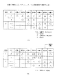
図12は従来のフラッシュEEPROMの記憶マップを示している。
FMEM1には切替データと警報データの各記憶領域が設けられており、夫々には例えば2セクタ分が固定的に割り当てられている。今、切替データのバックアップ処理について説明すると、例えばセクタ1が使用済み(データ書込完了)となった時は、未使用のセクタ2を次ブロックデータの書込先となし、古くなったセクタ1の記録データを消去する。このセクタ1の消去中は、セクタ2へのデータ書込を行えないが、BUF1があるので、切替データの取りこぼしは発生しない。セクタ3,4についても同様である。
【0010】
挿入図(a)にセクタ1の記憶マップを示す。
セクタ1は、セクタ1の管理情報を記録するためのヘッダ部と、監視データを格納するためのデータ部とを備える。
ヘッダ部において、運用状況フラグは自セクタ1の現在の運用状況を記録保持する。セクタ1が消去された時は、全ビット「1」となり、運用状況フラグ=0xffff(但し、0xはヘキサデシマル表示)となる。これはセクタ1が未使用(消去完了)であることを表す。次にセクタ1が使用中になると、運用状況フラグ=0x1000に書き換えられる。また寿命の来たセクタの運用状況フラグ=0x0000(使用不可)に書き換えられる。
【0011】
また、消去回数はセクタ1の消去回数をコード情報で保持する。具体的に言うと、最初は消去回数=0x0001(1回目)を書き込む。2回目は前記1回目と同一の欄又は次の欄に消去回数=0x0002(2回目)を書き込む。以上のことは、他のセクタについても同様である。
【0012】
【発明が解決しようとする課題】
しかし、上記FMEM1が1つであると、何れかのセクタが消去中の場合は他のセクタにアクセスできないため、不測の事態により監視データが大量に発生したような場合には、バッファメモリ36がオーバフローし、データの格納漏れが発生する。これを回避するにはバッファ36の容量を十分に大きくしておく必要があった。
【0013】
また、上記FMEM1が1つであると、FMEM1の寿命が尽きた場合には、ファイル盤30を止めて(引き抜いて)FMEM1を交換しない限りデータの格納が不可能となり、データバックアップ処理に支障を来していた。
また、上記データ種別毎に1セクタ(例えば64kバイト)分のバッファを設け、該バッファがフルになった時点でFMEM1にブロック書込を行う方式であると、データのブロック書き込みには時間を要するため、この区間に新たな監視データが発生すると、バッファへの次データ書込遅延が発生する。また、バッファ36のデータ蓄積中に電源OFFされる危険性も多分にあり、電源OFFされると、バッファ36の蓄積データが消滅してしまう。
【0014】
また、上記自セクタの管理情報を自セクタに記録する方式であると、自セクタを消去する度に消去前の管理情報(消去回数等)を外部のRAM等に退避させる必要がある。そして、この退避中にもし電源OFFが発生した場合には退避データが消滅してしまい、正確な寿命管理が不可能となる。
また、上記データ種別毎に複数のセクタを固定的に配分する方式であると、一部のセクタの寿命が尽きた場合や、あるデータ種別について書込処理がバースト的に発生したような場合には、未使用セクタが不足する場合がある。
【0015】
また、上記消去回数をコード情報で複数欄に記録する方式であると、FMEM1の記録欄が多数必要となり、メモリの節約とならない。
また、上記FMEM1へのデータ書込中をLEDの点滅等により外部に通知する方式であると、LED点滅の見落としによるファイル盤の誤引き抜きや、点滅開始前後の電源OFF操作等により、データを正常に格納できない場合がある。
【0016】
本発明は上記従来技術の欠点に鑑み成されたもので、その目的とする所は、消去後の記憶エリアにデータを書込可能な不揮発性メモリ媒体によるデータのバックアップを効率良くかつ確実に行えるデータバックアップ方式を提供することにある。
【0022】
【課題を解決するための手段】
上記の課題は例えば図1 の構成により解決される。即ち、本発明(1)のデータバックアップ方式は、消去後の記憶エリアにデータを書込可能な不揮発性メモリ媒体を使用したデータバックアップ方式において、同一種別のデータに対するデータ書込領域を複数の不揮発性メモリ媒体上に夫々設けると共に、データ種別毎に揮発性メモリからなる退避バッファを設け、通常は入力データを一旦前記退避バッファに記憶後、速やかに該記憶データを不揮発性メモリ媒体に書き込むと共に、該不揮発性メモリ媒体が書込不可状態にある場合は、入力データを順次前記退避バッファに蓄積し、前記不揮発性メモリ媒体が書込可能状態となった時点で前記退避バッファの蓄積データ分を該不揮発性メモリ媒体に書き込むものである。
【0023】
なお、図1 は複数が2の場合を示すが、3以上でも良い。また不揮発性メモリ媒体としては例えばフラッシュEEPROMを想定すると分かり易い。図において、本発明(1)においては、同一種別のデータ(例えばデータA)に対するデータ書込領域(データA書込領域)を複数の不揮発性メモリ媒体1,2上に夫々設けると共に、同一種別のデータAにつき、ある不揮発性メモリ媒体1の記憶データを消去する際には他の不揮発性メモリ媒体2に対して入力データAの書き込みを行う。従って、不揮発性メモリ媒体1が消去中でも、後続の入力データAを不揮発性メモリ媒体2に遅滞なく書き込め、こうして入力データのバックアップを効率良くかつ確実に行える。
更に、データ種別A,B毎に揮発性メモリからなる退避バッファA,Bを設け、通常は例えば入力データAを一旦前記退避バッファAに記憶後、速やかに該記憶データAを例えば不揮発性メモリ媒体1に書き込むと共に、該不揮発性メモリ媒体1が書込不可状態(例えばデータB書込領域1が消去中)にある場合は、入力データAを順次前記退避バッファAに蓄積し、前記不揮発性メモリ媒体1が書込可能状態(データB書込領域1が消去完了)となった時点で前記退避バッファAの蓄積データ分を該不揮発性メモリ媒体1に書き込む。
【0024】
即ち、本発明では入力データを不揮発性メモリ媒体1/2に直接書き込むのが基本であり、退避バッファA,Bは不揮発性メモリ媒体1/2へのデータ書き込みが待たされる時の2次的なデータ退避手段として位置付けられる。従って、不測の電源OFF等が発生しても、データを消失する可能性が少ない。
好ましくは本発明(2)においては、上記本発明(1)において、不揮発性メモリ媒体の挿抜を実質ロック/アンロック状態にするための挿抜機構部(不図示)を備え、退避バッファが不揮発性メモリ媒体への未格納データを保持している場合は前記挿抜機構部をロック状態にするものである。
【0025】
即ち、本発明(2)においては、例えば退避バッファAが不揮発性メモリ媒体1又は2への未格納データAを保持している場合は、不揮発性メモリ媒体1及び又は2をロック状態にして不揮発性メモリ媒体1及び又は2の取り外しを制限する。従って、未格納データAは不揮発性メモリ媒体に確実に保持され、一方、ユーザ(保守者等)が不用意に不揮発性メモリ媒体を外してしまうことを有効に防止できる。
【0026】
また本発明(3)においては、上記本発明(1)において、複数の不揮発性メモリ媒体についての運用状況を夫々に記録管理可能な管理データ記憶領域を前記複数の不揮発性メモリ媒体上に夫々設け、前記管理データ記憶領域は複数の不揮発性メモリ媒体についてのセクタ毎の運用状況を夫々に記録管理可能であると共に、ある不揮発性メモリ媒体の管理データ記憶領域を消去する前に、該管理データ記憶領域の最新の管理データを他の不揮発性メモリ媒体の管理データ記憶領域にコピーして前記複数の不揮発性メモリ媒体についての運用状況の管理を継続するものである。
【0027】
即ち、本発明(3)においては、例えば2つの不揮発性メモリ媒体1,2についての運用状況(使用中,使用済み,消去待ち等)を夫々に記録管理可能な管理データ記憶領域を前記2つの不揮発性メモリ媒体1,2上に夫々設けると共に、ある不揮発性メモリ媒体1の管理データ記憶領域を消去する前に、該管理データ記憶領域1の最新の管理データを他の不揮発性メモリ媒体2の管理データ記憶領域にコピーして前記2つの不揮発性メモリ媒体1,2についての運用状況の管理を継続する。
【0028】
従って、不揮発性メモリ媒体1を消去しても、不揮発性メモリ媒体2で不揮発性メモリ媒体1,2の運用状況を引き続き継続して管理できる。
また、不揮発性メモリ媒体1,2についての運用状況を不揮発性メモリ媒体上で記録管理することにより、装置の電源ON/OFFといった外的要因に影響される事無く、不揮発性メモリ媒体1,2の運用状況や寿命を一貫して正確に管理することが可能となる。
【0031】
また好ましくは本発明(4)においては、上記本発明(1)において、不揮発性メモリ媒体は記憶データをセクタ単位に消去可能であると共に、1つの不揮発性メモリ媒体につき1つのデータ種別に対して複数のセクタをデータ書込領域に割り当て、ある不揮発性メモリ媒体につきに複数のセクタを使用した後、他の不揮発性メモリ媒体につきに複数のセクタを使用すると共に、前記ある不揮発性メモリ媒体の複数のセクタを適宜のタイミングに消去し、こうして複数の不揮発性メモリ媒体につきに複数のセクタを巡回的に使用する。
【0032】
即ち、本発明(4)においては、例えばある不揮発性メモリ媒体1につきに2つのセクタを使用した後、他の不揮発性メモリ媒体2につきに2つのセクタを使用すると共に、前記ある不揮発性メモリ媒体1の2つのセクタを適宜のタイミングに消去し、こうして2つの不揮発性メモリ媒体1,2につきに2つのセクタを巡回的に使用する。従って、限られた容量の不揮発性メモリ媒体1,2を多くのデータ種別により夫々に効率良く確実に利用できる。
【0033】
また好ましくは本発明(5)においては、上記本発明(4)において、ある不揮発性メモリ媒体のあるセクタを使用中に、他の不揮発性メモリ媒体2が交換を必要とする状態にある場合は、前記ある不揮発性メモリ媒体の使用済みセクタを消去する。即ち、本発明(5)においては、例えばデータA書込領域1を使用後、続けてデータA書込領域2を使用する時に、他の不揮発性メモリ媒体2が交換(例えば寿命等による交換)を必要とする状態にある場合は、旧データA書込領域1を消去する。従って、かかる場合でもデータAの書込を継続でき、システムを止めること無く不揮発性メモリ媒体2を交換できる。
【0034】
また好ましくは本発明(6)においては、上記本発明(4)において、予め割り当てた数のセクタが不足状態に至った場合は、他のセクタを新たに割り当てる。例えばデータAのデータ量が増した場合、又は不揮発性メモリ媒体1のデータA書込領域1,2を使用後、不揮発性メモリ媒体1,2のいずれにも未使用のデータA書込領域が見つからないような場合には、好ましくは他の割当外のセクタを新たにデータA書込領域3等として割り当てる。又は、他の割当外のセクタが存在しないような場合には、例えば他のデータ種別Bに割り当ててあったセクタの割当を変更してデータ種別Aの側に割り当てる。従って、このようなセクタの柔軟な再割当てにより、データの格納漏れを有効に回避できる。
【0038】
【発明の実施の形態】
以下、添付図面に従って本発明に好適なる実施の形態を詳細に説明する。なお、全図を通して同一符号は同一又は相当部分を示すものとする。
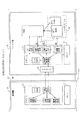
図2は実施の形態によるデータバックアップ方式の構成を示す図で、上記図11と同様に冗長構成を有するデータ伝送システムにおける伝送路監視装置の一部構成(主に監視データのバックアップ記憶に係る構成)を示している。
【0039】
図において、10は制御盤(基板,パッケージ等)、11はCPU1、12は主メモリ(MM1)、13は制御盤の挿抜を制限するためのパッケージ挿抜機構部、13aはそのロックピン、30はファイル盤、31はCPU2、32は主メモリ(MM2)、33はパッケージ挿抜機構部、33aはそのロックピン、34はDPRAM、35はデータ伝送システムの各種監視データ(回線切替データ,回線警報データ等)及びこれらの記録管理に係る管理データをバックアップ(不揮発に)保持するバックアップメモリモジュール、FMEM1,2はフラッシュEEPROM、36は制御盤から送られる各種監視データを一時的に蓄積するバッファメモリモジュール、BUF1,2は夫々1セクタ分の記憶容量を有するバッファメモリ(RAM)である。
【0040】
制御盤10において、通信制御処理は伝送路監視装置に必要なデータ通信制御を行う。切替管理処理は回線の冗長切替に関する監視データを収集管理する。警報管理処理は回線に関する各種警報データを収集管理する。FMEM管理処理は前記収集された各種データをファイル盤に格納するためのインタフェース処理を行う。そして、上記各処理はタスクとして構成され、OS処理の管理下で適宜に実行される。
【0041】
ファイル盤30において、FMEM制御処理はFMEM管理処理との間のデータやメッセージのやり取りをインタフェースすると共に、ファイル盤におけるデータ読書制御及びFMEM1,2の消去制御等を管理する。バッファ退避処理は制御盤から送られる各種データを一時的にバッファメモリモジュール36に記憶する。FMEM書込処理はBUF1又は2の未格納デ−タを速やかにFMEM1又は2に書き込み、必要なら管理セクタの管理データ(セクタ運用状況フラグ,データ種別等)を更新管理する。FMEM読出処理はFMEM1,2からデータを直接に読み出す。セクタ消去処理は消去待ちのセクタを消去し、必要なら管理セクタの管理データ(セクタ消去回数等)を更新管理する。そして、上記各処理はタスクとして構成され、OS処理の管理下で適宜に実行される。
【0042】
パッケージ挿抜機構部13は、図示しないが、内部にソレノイド機構部等を備えており、CPU1からのロック信号LK1=1の時はロックピン13aを図の上側に押し出して制御盤10をスロット100から引き抜けないようにロックし、またロック信号LK1=0の時はロックピン13aを図の下側に引っ込めて制御盤10をスロット100から引き抜けるようにアンロックする。パッケージ挿抜機構部33についても同様である。
【0043】
なお、図示しないが、制御盤10は電源スイッチのOFF操作を保持するステータスレジスタを備えており、OFF操作=1の時はCPU1が本装置への給電をOFFにする。
バックアップメモリモジュール35は、少なくとも2つのフラッシュEEPROM素子(FMEM1,2)を備えている。素子1個当たりの記憶容量は例えば512kバイトであり、1セクタ(=64kバイト)×8セクタからなっている。各素子は1セクタ毎に消去可能であり、1セクタ当たりの消去時間は1.5〜30秒程度である。またセクタ消去中の素子には同時にデータアクセス(書込)を行えない。そして、消去回数は有限(例えば10万回)である。また、この例のフラッシュEEPROMでは消去(リセット)後のデータは全ビット「1」となり、ビット「0」のみを上書可能である。なお、消去後のデータが全ビット「0」となり、ビット「1」のみを上書可能な素子を使用しても良い。
【0044】
バッファメモリモジュール36において、退避バッファBUFはデータ種別毎に備える。この例では切替データ用に1個(BUF1)、警報データ用に1個(BUF2)を備える。なお、1つのRAMの記憶領域を分割してBUF1,2としても良いことは明らかである。また、退避バッファはプログラムにより選択可能であり、いずれが切替データ用又は警報データ用でも良い。
【0045】
また本実施の形態によるデータバックアップ方式では、制御盤10から送られる各種データをフラッシュEEPROM35に直接書き込むのが基本であり、退避バッファ(RAM)36はフラッシュEEPROM35へのデータ書き込みが待たされる時の一時的なデータ退避手段として位置付けられる。
図3,図4は実施の形態によるフラッシュメモリ(フラッシュEEPROM)の記憶マップを説明する図(1),(2)である。
【0046】
なお、以下の説明はFMEM1について行うが、FMEM2についても同様である。またFMEM2のセクタ11〜1nはFMEM1のセクタ1〜nと説明上区別するための表記であり、FMEM2のセクタ1〜nと呼んでも良い。
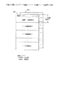
図3はFMEM1における管理データ記憶領域の詳細を示している。
FMEM1には管理データ記憶領域(セクタ1,2)と情報データ記憶領域(セクタ3〜n)とが含まれる。
【0047】
挿入図(a)に管理データ記憶領域中のセクタ1の記憶マップを示す。
セクタ1にはm個分の管理領域1〜mが含まれる。また管理領域1には2n個分のセクタ1管理領域〜セクタ1n管理領域が含まれる。因みに、n=8より、セクタ1管理領域=8×16=128バイトになるから、m=64k/128=500となる。
【0048】
セクタ1におけるセクタ1管理領域ではセクタ1(自セクタ)の運用状況を管理し、セクタ2管理領域ではセクタ2の運用状況を管理し、以下同様にして進み、セクタ1n管理領域ではセクタ1nの運用状況を管理する。
従って、最初はセクタ1の管理領域1を使用してシステムの全セクタ1〜n,11〜1nの管理を行える。そして、何れかのセクタi管理領域で管理データを更新不可能(例えばビット「0」から「1」への書換が必要)となった様な場合には、管理領域1の全情報を管理領域2にコピーして管理を続ける。但し、上記更新不可能となったセクタi管理領域のデータについては、そのままコピーするのでは無く、更新不可能となった部分(例えば消去回数等)につき新たに管理を続けられるようにその内容を初期化する。
【0049】
次にセクタ1管理領域の内容を説明する。
「運用状況フラグ」(2バイト)は管理対象セクタの運用状況を表す。セクタ1を消去(リセット)すると全ビット「1」となる。従って、運用状況フラグ=0xffffとなる。その後は、管理対象セクタの運用状況の変化に伴い、対応ビットに「0」を書き込むことで、各種の運用状況をセクタ1の消去なしに表せる。一例のセクタ運用状況の内容(遷移)とその運用状況フラグを示すと、
「消去中」:0xffff(消去により全ビット「1」となる)
「未使用(消去完了時):0x7fff(ビット15を「0」にする)
「使用中」:0x3fff(ビット14を「0」にする)
「使用済み」:0x1fff(ビット13を「0」にする)
「消去待ち」:0x0fff(ビット12を「0」にする)
「使用不可(寿命等)」:上記コード以外
となる。
【0050】
「データ種別」(2バイト)は管理対象セクタに記憶すべきデータの種別を表す。一例のデータ種別とその符号を示すと、
セクタ1,2のデータ種別=「管理データ」:0x1000
セクタ3,4のデータ種別=「切替データ」:0x0001
セクタ5,6のデータ種別=「警報デ−タ」:0x0010
となる。ここで、「管理データ」はセクタ1〜n,11〜1nを管理するためのデータ種別、「切替データ」は2重化冗長構成を採るデータ伝送システムの冗長切替履歴に関するデータ種別、「警報デ−タ」は回線障害,ビットエラーレート等の警報履歴に関するデ−タ種別を夫々表す。
【0051】
「消去回数」(4バイト)は管理対象セクタの消去回数を表す。「消去回数」の欄は一種のカウンタとして働き、その下位2バイトは管理対象セクタの消去毎に最下位ビットから順に1ビットを落とすことで16回分の消去回数を連続して(セクタ1の消去無しで)カウント可能である。一方、上位2バイトは16の倍数分の消去回数をバイナリーコーデッドデシマル方式により0〜6万4千回までカウントする。従って、トータルでは64000×16≒102万回をカウント可能であり、通常のフラッシュEEPROMの消去限度回数(10万回程度)を十分にカバーできる。
【0052】
一例の消去回数の内容(遷移)を示すと、
リセット時 :0xffffffff(消去により全ビット「1」となる)
初期値書込時:0x0000ffff(管理領域1への初期値書込時)
1回目消去時:0x0000fffe(最下位ビットLSBを落とす)
2回目消去時:0x0000fffc(LSBから2番目を落とす)
16回目消去時:0x00000000(LSBから16番目を落とす)
管理領域変更時:0xffffffff(全ビット「1」となっている)
初期値書込時:0x0001ffff(管理領域2への初期値書込時)
17回目消去時:0x0001fffe(LSBを落とす)
18回目消去時:0x0001fffc(LSBから2番目を落とす)
となる。
【0053】
ここで、上記管理領域1から管理領域2への領域変更は、例えば何れかの管理対象セクタの消去回数が16回を越えた時に発生する。即ち、当該セクタの「消去回数」は16回目消去時に0x00000000となったため、これ以上の消去回数は管理領域1では計数できない。この場合は、まず管理領域1の全情報(但し、消去回数=0x00000000の欄を除く)を管理領域2にコピーする。この時、管理領域2における上記消去回数=0x00000000の対応欄では予め消去回数=0xffffffffとなっているから、ここに消去回数の初期値=0x0001ffffを書き込む。以下、同様にして進み、管理領域mに遷移するまではカウンタの上位2バイトを連続して(セクタ1を消去すること無しに)更新できる。即ち、セクタ1では、ある管理対象セクタにつき最大m(=500)×16=8000回までの消去回数を連続して計数できる。
【0054】
こうして、セクタ1の全管理領域を使い切った時は次にセクタ2を使用し、更にセクタ2を使い切った時は次にセクタ11を使用する。好ましくは、この区間に古くなたセクタ1,2の管理データを消去する。更に上記セクタ11を使い切った時は次にセクタ12を使用する。因みに、このセクタ12を使い切るまでに単純計算では、ある管理対象セクタにつき最大8000×4=32000回までの消去回数を連続して計数できる。そして、セクタ12を使い切った時は、次に既に消去済みのセクタ1を巡回的に使用する。従って、その先の消去回数も実質連続して計数できる。
【0055】
図4はFMEM1の情報デ−タ記憶領域の詳細を示している。
情報データ記憶領域(セクタ3〜n)にはデータ種別(切替データ,警報データ等)毎に夫々2つのセクタが割り当てられている。なお、以下は切替データについて説明するが、警報データについても同様である。
挿入図(a)に切替データ記憶領域中のセクタ3の記憶マップを示す。
【0056】
セクタ3にはk個分のデータ領域1〜kが含まれる。またデータ領域1にはヘッダ領域とデータ格納領域とが含まれる。
一例のデ−タ領域の内容は、
「Ser.No.」(8バイト):格納データの通番
「格納開始アドレス」(8バイト):データの格納開始アドレス
「データ長」(2バイト):格納データのサイズ
「書込完了フラグ」(2バイト):データ書込完了(0x5aa5)
「データ格納領域」:格納すべき実データ(サイズは予め任意に決定可)
である。
【0057】
係る構成により、まず最初の切替データが発生すると、セクタ3のデータ領域1に書き込む。次に2番目の切替データが発生すると、同セクタ3のデータ領域2に書き込む。以下、同様にして進み、k番目の切替データが発生すると、同セクタ3のデータ領域kに書き込む。更に、こうして、セクタ1の全データ領域を使い切った時は次にセクタ4を使用し、更にセクタ4を使い切った時は次にセクタ13を使用する。好ましくは、この区間に古くなたセクタ3,4の切替データを消去する。更に上記セクタ13を使い切った時は次にセクタ14を使用する。そして、セクタ14を使い切った時は、次に既に消去済みのセクタ3を巡回的に使用する。こうして、セクタ3,4,13,14に実質連続して切替データを書き込める。
【0058】
図5は実施の形態によるフラッシュメモリの巡回的使用を説明する図で、図5(A)はフラッシュEEPROMの寿命が未だ尽きていない通常の場合を示している。今、切替データの処理を例に説明すると、FMEM1につきセクタ3,4、及びFMEM2につきセクタ13,14を巡回的に使用する。
図において、各記号は管理対象セクタの運用状況フラグを表しており、空白は「未使用(消去完了)」、○印は「使用中」、△印は「使用済み/消去待ち」、×印は「消去中」、××印は「使用不可(寿命)」を夫々表す。
【0059】
状態1では、セクタ1におけるセクタ3管理領域1の運用状況フラグを「使用中」となし、その後に発生した各切替データをセクタ3の各データ領域1,2,…,に順次書き込む。やがて、セクタ3にk番目の切替データを書き込むと、状態2に移る。
状態2では、上記セクタ1におけるセクタ3管理領域1の運用状況フラグを「使用済み」、かつセクタ4管理領域1の運用状況フラグを「使用中」となし、その後に発生した各切替データをセクタ4の各データ領域1,2,…,に順次書き込む。やがて、セクタ4にk番目の切替データを書き込むと、状態3に移る。
【0060】
状態3では、上記セクタ1におけるセクタ4管理領域1の運用状況フラグを「使用済み」、かつセクタ13管理領域1の運用状況フラグを「使用中」となし、その後に発生した各切替データをセクタ13の各データ領域1,2,…、に順次書き込む。やがて、セクタ13にk番目の切替データを書き込むと、状態4に移る。
【0061】
状態4では、上記セクタ1におけるセクタ13管理領域1の運用状況フラグを「消去待ち」、かつセクタ14管理領域1の運用状況フラグを「使用中」となし、その後に発生した各切替データをセクタ14の各データ領域1,2,…、に順次書き込む。
一方、この時点でFMEM1については新たにデータを書き込む必要は無いので、上記セクタ1におけるセクタ3,4管理領域1の各運用状況フラグを「消去待ち」にする。これによりFMEM1のセクタ3,4が順次消去され、消去完了すると、上記セクタ1におけるセクタ3,4管理領域1の各運用状況フラグを「消去完了(未使用)」にする。
【0062】
ところで、この時、上記セクタ1におけるセクタ3,4管理領域1の各運用状況フラグは既に「消去待ち」=0x0fffにされていたため、このまま(即ち、セクタ1の消去なし)では、各運用状況フラグを元の「未使用」=0xffffには戻せない。そこで、この場合は、上記既に「消去待ち」=0x0fffとされた各運用状況フラグの下から3番面の各4ビット情報「f」を使用することにより、その後の各運用状況フラグの更新管理をセクタ1の消去無しに継続できる。
【0063】
一方、セクタ1におけるセクタ3,4管理領域1の各消去回数は0x0000ffffから0x0000fffeとされる。従って、以後はこの消去回数を参照する(即ち、消去回数と運用状況フラグの使用領域とを連動させる)ことにより、例えば上記運用状況フラグについては下から3番面の4ビット情報「f」を使用すれば良いことが分かる。因みに、セクタ3,4管理領域1の各消去回数=0x0000fffcとなった時は、各運用状況フラグの下から2番面の各4ビット情報「f」を使用することにより各運用状況フラグの更新管理をセクタ1の消去無しに継続できる。
【0064】
ところで、これでは、上記消去回数を16回分連続して計数できるのに、運用状況フラグについては4回分しか連続して更新管理できないことになり、アンバランスが生じる。この場合は、例えば運用状況フラグのビット数を増せば良い。即ち、例えば運用状況フラグ(8バイト)=0xffffffffffffffffとすれば良い。
【0065】
なお、上記の方法に代え、管理対象セクタを消去する度に、セクタ1における管理領域を管理領域1,2,…,の如く移していっても良い。
主題に戻り、上記状態4では、FMEM2については消去作業を行っていないので、セクタ14へのデータ書込が遅延することは無い。こうして、やがてセクタ14にk番目の切替データを書き込むと、状態5に移る。
【0066】
状態5では、セクタ1におけるセクタ14管理領域1の運用状況フラグを「使用済み」、かつセクタ3管理領域1の運用状況フラグを「使用中」となし、その後に発生した各切替データをセクタ3の各データ領域1,2,…,に順次書き込む。やがて、セクタ3にk番目の切替データを書き込むと、状態6に移る。
状態6では、セクタ1におけるセクタ3管理領域1の運用状況フラグを「使用済み」、かつセクタ4管理領域1の運用状況フラグを「使用中」となし、その後に発生した各切替データをセクタ4の各データ領域1,2,…,に順次書き込む。一方、この時点でFMEM2については新たにデータを書き込む必要は無いので、セクタ13,14管理領域1の各運用状況フラグを「消去待ち」にする。こうして、やがてセクタ4にk番目の切替データを書き込むと、状態7に移る。以下、同様である。
【0067】
図5(B)はFMEM1の寿命が尽きた場合の処理を示している。
状態3までは上記と同様で良い。状態4では、セクタ1におけるセクタ14管理領域1の運用状況フラグを「使用中」となし、その後に発生した各切替データをセクタ14の各データ領域1,2,…,に順次書き込む。
一方、この時点ではセクタ3,4の消去回数は限界値となっており、これ以上はセクタ3,4を使用しない方が良い。そこで、この場合はセクタ1におけるセクタ3,4管理領域1の各運用状況フラグを「使用不可(寿命)」にし、好ましくは、その旨がランプの点滅等により外部(保守者等)に知らされる。
【0068】
また、セクタ1におけるセクタ13管理領域1の運用状況フラグを、これまで行ってきた「使用済み」に代えて、「消去待ち」とする。これによりセクタ13は速やかに消去開始される。こうして、やがてセクタ14にk番目の切替データを書き込むと、状態5に移る。
状態5では、通常それまでにはセクタ13の消去が完了していることにより、セクタ1におけるセクタ13管理領域1の運用状況フラグを「使用中」となし、その後に発生した各切替データをセクタ13の各データ領域1,2,…,に順次書き込む。また、セクタ1におけるセクタ14管理領域1の運用状況フラグを「消去待ち」となし、これによりセクタ14は速やかに消去開始される。こうして、やがてセクタ14にk番目の切替データを書き込むと、状態6に移る。
【0069】
状態6では、セクタ1におけるセクタ14管理領域1の運用状況フラグを「使用中」となし、その後に発生した各切替データをセクタ14の各データ領域1,2,…,に順次書き込む。
そして、この例では、上記ランプの点滅に気づいた保守者が、システムを止めること無く、上記セクタ3,4で寿命の尽きたFMEM1を取り外し、代わりに新品のFMEM1を挿入する。これにより、セクタ1におけるセクタ13管理領域1の運用状況フラグは「使用済み」とされる。こうして、やがてセクタ14にk番目の切替データを書き込むと、状態7に移り、以後は上記通常の場合と同様に処理が進む。
【0070】
このように本実施の形態によれば、どちらかのフラッシュEEPROMの寿命が尽きた場合でも、残りのフラッシュEEPROMを使用してデータバックアップの縮退運用が可能である。
或いは、他の空きセクタ又は他のデータ種別にアサインされているセクタのデータ種別を変更して当該不足の生じたデータ種別にアサインすることにより、一部のセクタに寿命の来たフラッシュEEPROMを交換すること無く、そのままデータバックアップ処理を継続することが可能である。
【0071】
なお、あるデータ種別に対するセクタの不足は、当該データ種別のデータがバースト的に発生した場合にも起こり得るが、この場合も上記他のセクタをアサインする方法が有効である。
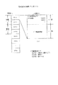
図6は実施の形態によるデータ退避バッファ36の記憶マップを説明する図である。
【0072】
なお、上記の如くこのデータ退避バッファ(RAM)36はフラッシュEEPROM35へのデータ書き込みが待たされる時の一時的なデータ退避手段として位置付けられるものであり、その様な状況が起こらない用途(データ発生量が少ない等)では、このデータ退避バッファ(RAM)36を省略できる。
図において、データ種別毎に退避バッファBF1,BF2(例えば各64kバイト)を設け、入力データを一旦本退避バッファに記憶すると共に、FMEM1/2がデータ書込可能な場合は、直ちに本退避バッファから1入力データ単位(ハード的には例えばバイト単位)にデータを読み出し、FMEM1/2に書き込む。
【0073】
退避バッファBUF1,2は、夫々の入力データをデータ入力単位で十分に記憶可能な複数のデータ退避領域1〜j,11〜1jに分割されており、その使用/未使用(データ格納有/無)を退避チェックフラグにより管理する。
一例の退避チェックフラグの内容は、
「バッファ非退避時」:0x0000
「バッファ退避時」 :0x0001
である。
【0074】
各退避バッファBUF1,2は、所謂FIFO型バッファとして運用され、最初の入力データはデータ退避領域1/11に書き込まれ、該領域1/11から最初に読み出される。2番目の入力データはデータ退避領域2/12に書き込まれ、該領域2/12から2番目に読み出される。以下、同様にして進み、最後のデータ退避領域j/1jが使用されると、今度は先頭のデータ退避領域1/11からサイクリックに使用される。
【0075】
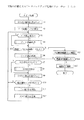
図7〜図10は実施の形態によるデータバックアップ処理のフローチャート(1)〜(4)である。
図7はメイン処理を示しており、主に図2のCPU2のOS処理及びFMEM制御処理で実行される。
ステップS1では全タクスの運用状況をチェックし、ステップS2ではデータ種別対応にデータ退避バッファを割り当てる。ステップS3では制御盤10からのデータ書込要求があるか否かを判別し、ある場合はステップS4で入力データを一旦対応する退避バッファに書き込み、ステップS5に進む。またデータ書込要求がない場合はステップS4の処理をスキップする。
【0076】
ステップS5では退避バッファに未格納データがあるか否かを判別し、ある場合はステップS6で退避データをFMEM1/2に書き込み、ステップS7に進む。また無い場合は、ファイル盤30を取り外しても支障がないので、ステップS13ではパッケージ挿抜機構部33のロック状態を解除する。ステップS14では電源OFF制御ありか否かを判別し、なしの場合はステップS7に戻る。またありの場合はステップS15で電源をOFFにし、処理終了となる。なお、上記ステップS14,15の各処理はむしろ図2のCPU1が行っても良い。
【0077】
更に、ステップS7では消去待ちのセクタがあるか否かを判別し、ある場合はステップS8で当該セクタを消去する。また消去待ちのセクタが無い場合はステップS8の処理をスキップする。
ステップS9では全セクタにつき消去回数をチェックする。ステップS10では規定値オーバ(寿命)のセクタがあるか否かを調べ、ない場合はステップS3に戻る。またある場合はステップS11でアラーム信号を発出し、その旨を外部(保守者等)に知らせる。ステップS12ではデータを記憶するためのセクタの割当を更新(変更)する。即ち、規定値オーバ(寿命)のセクタを使用しているデータ種別に対して、他の空きセクタ、又は他のデータ種別にアサインされているセクタを割り当てる。
【0078】
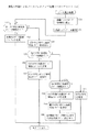
図8はデータ退避バッファへのデータ退避処理を示しており、主に図2のCPU2のバッファ退避処理で実行される。
ステップS21では入力データに対応するデータ退避バッファに空き退避領域があるか否かを判別する。ある場合はステップS22で空き領域に入力データを書き込む。ステップS23では退避チェックフラグを「使用中」(データあり)にする。ステップS24では、退避バッファの記憶データがファイル盤30の抜き取りにより消えないように、パッケージ挿抜粋機構部33をロック状態にする。ステップS25では制御盤10に書込完了を通知し、この処理を抜ける。
【0079】
また上記ステップS21の判別で空き退避領域がない場合はステップS26で制御盤10に書込失敗を通知し、この処理を抜ける。
図9はデータ退避バッファからフラッシEEPROMへのデータ書込処理を示しており、主に図2のCPU2のFMEM書込処理で実行される。
ところで、退避バッファのデータを書込領域に制限のあり得るFMEMに書き込む場合には、データを書き込む際に未使用書込領域を探査する方法と、予め前回のデータ書込後に次回の未使用書込領域を確保しておき、次回のデータ書込の際には遅滞無くデータを書き込める方法とが考えられる。ここでは後者の場合を説明する。
【0080】
ステップS30では退避バッファのデータを予め確保されたFMEM1/2の未使用領域に書き込む。この時、必要なヘッダ情報も併せて書き込む。ステップS31では退避バッファの当該退避チェックフラグを「未使用」にする。ステップS32では同一セクタ内に未使用のデータ領域があるか否かを判別する。ある場合はステップS33で前記未使用のデータ領域にポインタ(次データの書込アドレス)を変更して処理を抜ける。なお、この種のポインタ情報については、電源OFF等により消滅しないように、フラッシュEEPROM上の適当なエリアで管理(又はバックアップ保持)するようにしても良い。
【0081】
また上記ステップS32の判別で未使用のデータ領域が無い場合は、ステップS34で当該セクタに対する運用状況フラグを「使用済み」にする。ステップS35では同一素子の他のセクタに未使用のデータ領域があるか否かを判別する。ある場合はステップS36で当該他のセクタの未使用データ領域にポインタを変更する。ステップS37では当該他のセクタに対する運用状況フラグを「使用中」にし、処理を抜ける。
【0082】
また上記ステップS35の判別で同一素子の他のセクタにも未使用のデータ領域がない場合は、ステップS38で他のFMEMに未使用データ領域があるか否かを判別する。未使用データ領域がある場合はステップS39で当該他のFMEMの未使用データ領域にポインタを変更する。ステップS40では当該他のFMEMのセクタに対する運用状況フラグを「使用中」にする。ステップS41では旧FMEMの各データ用セクタに対する運用状況フラグを「消去待ち」にする。
【0083】
また上記ステップS38の判別で他のFMEMにも未使用データ領域がない場合はステップS42で当該データ種別に対するセクタの割当てを変更する。又は、図示しないが、データ用セクタが無い旨のエラーフラグを立てても良い。そして、処理を抜ける。
図10はセクタ消去処理を示しており、主に図2のCPU2のセクタ消去処理で実行される。
【0084】
ステップS50では運用状況フラグが「消去待ち」となっているセクタを消去する。ステップS51では消去済みセクタに対する運用状況フラグを「未使用」にする。ステップS52では消去したセクタに対する消去回数に+1する。ステップS53では当該消去回数が続けて更新可能(即ち、カウンタの下位16ビットを順次落とすことで計数可能)か否かを判別する。更新可能の場合は処理を抜ける。また更新可能でない場合はステップS54で同一セクタ内に未使用の管理領域があるか否かを判別する。ある場合はステップS55で未使用の管理領域に全セクタ分の管理情報を遷移させる。この時、前記更新不可能となったセクタを管理する新たな管理領域では、消去回数カウンタの上位16ビットに+1され、下位16ビットの内容は0xffffに初期化される。そして、処理を抜ける。
【0085】
また上記ステップS54の判別で同一セクタ内に未使用の管理領域が無い場合はステップS56で同一素子内の他のセクタに未使用の管理領域があるか否かを判別する。ある場合はステップS57で当該同一素子内の他のセクタの未使用管理領域に全管理情報を遷移させ、処理を抜ける。
また上記ステップS56の判別で同一素子内の他のセクタにも未使用の管理領域が無い場合はステップS58で他のFMEMに未使用の管理領域があるか否かを判別する。ある場合はステップS59で当該他のFMEMの未使用管理領域に全管理情報を遷移させる。ステップS60では旧FMEMの各管理用セクタに対する運用状況フラグを「消去待ち」にする。
【0086】
また上記ステップS58の判別で他のFMEMにも未使用の管理領域がない場合はステップS61で管理データに対するセクタの割当てを変更する。又は、図示しないが、管理用セクタが無い旨のエラーフラグを立てても良い。そして、処理を抜ける。
なお、図7に戻り、上記の例は退避バッファBUF1/2に溜まったデータを何時でもFMEM1/2に書き込める場合を述べた。例えば切替データのみにつきセクタ3,4,13,14を巡回使用するような場合にあっては、大抵の場合にこの様な状況が維持され得る。従って、退避バッファは特に必要ない。
【0087】
しかし、同時に警報データについてもセクタ5,6,15,16を巡回使用するような場合には、これらの間のデータ発生量等の相違から、例えばセクタ3に切替データの書込を行おうとした時に、たまたまセクタ5又は6が「消去中」と言う場合も起こり得る。
係る場合には、図7のステップS5とS6の間に、データ書込対象の素子が消去中か否かを判別し、消去中の場合はステップS6の処理をスキップするような新たなステップを設ければ良い。これにより、退避バッファには次々と切替データが蓄積され、やがて、セクタ5及び6が「消去完了」になると、退避バッファに蓄積された切替データがセクタ3に書き込まれる。
【0088】
なお、上記実施の形態では消去後の記憶エリアにデータを書込可能な不揮発性メモリ媒体としてフラッシュEEPROMを使用した場合を述べたが、本発明は、消去後の記憶エリアにデータを書き込むと言う記録原理が同一であり、且つ異なる構造・形態を有する様な他の光磁気ディスク,相転移型ディスク等の不揮発性メモリ媒体にも適用できることは明らかである。
【0089】
また、上記実施の形態ではバッファメモリモジュール36を備える場合を述べたが、バッファメモリモジュール36を備えなくても本発明を実現できることは明らかである。
また、上記本発明に好適なる実施の形態を述べたが、本発明思想を逸脱しない範囲内で各部の構成、制御、及びこれらの組合せの様々な変更が行えることは言うまでも無い。
【0090】
【発明の効果】
以上述べた如く本発明によれば、上記消去後の記憶エリアにデータを書込可能な不揮発性メモリ媒体(特にフラッシュEEPROM)が有する様々な制約を克服できると共に、このような不揮発性メモリ媒体を使用したデータのバックアップを効率良くかつ確実に行える。
【図面の簡単な説明】
【図1】本発明の原理を説明する図である。
【図2】実施の形態によるデータバックアップ方式の構成を示す図である。
【図3】実施の形態によるフラッシュメモリの記憶マップを説明する図(1)である。
【図4】実施の形態によるフラッシュメモリの記憶マップを説明する図(2)である。
【図5】実施の形態によるフラッシュメモリの巡回的使用を説明する図である。
【図6】実施の形態によるデータ退避バッファの記憶マップを説明する図である。
【図7】実施の形態によるデータバックアップ処理のフローチャート(1)である。
【図8】実施の形態によるデータバックアップ処理のフローチャート(2)である。
【図9】実施の形態によるデータバックアップ処理のフローチャート(3)である。
【図10】実施の形態によるデータバックアップ処理のフローチャート(4)である。
【図11】従来技術を説明する図(1)である。
【図12】従来技術を説明する図(2)である。
【符号の説明】
10 制御盤(基板,パッケージ等)
11,31 CPU(CPU1,2)
12,32 主メモリ(MM1,2)
13,33 パッケージ挿抜機構部
13a,33a ロックピン
30 ファイル盤(基板,パッケージ等)
34 デュアルポートRAM(DPRAM)
35 バックアップメモリモジュール
36 バッファメモリモジュール
100 スロット
101 バックプレーン(BP)
BUF1,2 バッファメモリ(RAM)
FMEM1,2 フラッシュEEPROM[0001]
BACKGROUND OF THE INVENTION
The present invention relates to a data backup system, and more particularly to a data backup system for recording (storing) input data in a nonvolatile manner using a nonvolatile memory medium capable of writing data in a storage area after erasure.
In recent years, the size of system data (system operation data, system monitoring data, etc.) required for the operation of such devices in data transmission systems has tended to increase, and how efficient and reliable this data is. It is important to record in At the same time, there is a demand for miniaturization of the device. Therefore, in recent years, a nonvolatile memory (EEPROM) that is small in size and has a short data reading time compared to other storage media such as a hard disk is used as a data storage medium. Often used. Among them, the flash EEPROM has a large storage capacity, and thus the number of devices equipped with the flash EEPROM has increased in recent years.
[0002]
In the flash EEPROM, the operation of the byte rewritable EEPROM is divided into an erase operation and a data write operation. After the element or a part of a specified block (hereinafter also referred to as a sector) is erased collectively, the erased portion is erased. The data can be written electrically. Incidentally, NOR type flash EEPROMs are used as ROMs and data ROMs for mobile device control because of their fast data random read time due to their element structure, and NAND type flash EEPROMs have an element structure suitable for large capacity. Suitable for replacement of hard disks and floppy disks, etc., because the entire memory space can be divided and managed by a predetermined size (for example, 64 kB / sector), and the reading speed of block data in units of sectors is high. ing.
[0003]
However, in the flash EEPROM, the erase time of the element or sector is long (for example, about 1.5 to 30 seconds per sector), other sectors cannot be accessed during sector erase, and all the data after erase is all bits. Only the bit “0” can be overwritten in the element that becomes “1”, or only the bit “1” can be overwritten in the element in which the data after erasure becomes all the bits “0”, In addition, there are many restrictions on use, such as a limited number of erasures of elements and sectors (for example, about 100,000 times).
[0004]
Therefore, it is desired to provide an efficient data backup method that overcomes such limitations.
In addition to the flash EEPROM, a magneto-optical disk, a phase transition disk, and the like are known as a nonvolatile memory medium capable of writing data in a storage area after erasure. It can be used for a data backup method using a memory medium.
[0005]
[Prior art]
11 and 12 are views (1) and (2) for explaining the prior art.
FIG. 11 shows a partial configuration of a transmission line monitoring device (mainly related to backup storage of monitoring data) in a data transmission system having a conventional redundant configuration.
In the figure, 100 is a slot for detachably supporting a board (package) or the like in the rack construction apparatus, 101 is a common backplane (BP) for connecting signals between boards, and 10 is the main control of the transmission line monitoring apparatus. A control panel (board, package, etc.), 11 is a
[0006]
In the
[0007]
Similarly, in the
[0008]
With this configuration, the conventional data backup method basically stores various data sent from the
[0009]
FIG. 12 shows a storage map of a conventional flash EEPROM.
FMEM 1 is provided with storage areas for switching data and alarm data, and for example, two sectors are fixedly allocated. Now, switching data backup processing will be described. For example, when
[0010]
Inset (a) shows a storage map of
In the header part, the operation status flag records and holds the current operation status of the
[0011]
Further, the erase count holds the erase count of
[0012]
[Problems to be solved by the invention]
However, if there is one FMEM1, if any sector is being erased, other sectors cannot be accessed. Therefore, if a large amount of monitoring data is generated due to an unexpected situation, the
[0013]
Further, if the number of the
Further, when a buffer for one sector (for example, 64 kbytes) is provided for each data type and block writing is performed on the
[0014]
Further, in the method of recording the management information of the own sector in the own sector, it is necessary to save the management information (erase count etc.) before erasure to an external RAM or the like every time the own sector is erased. If the power is turned off during the saving, the saved data is lost, and accurate life management becomes impossible.
In addition, when a plurality of sectors are fixedly allocated for each data type, when some sectors have reached the end of their life or when write processing occurs in bursts for a certain data type. May run out of unused sectors.
[0015]
In addition, when the number of times of erasure is recorded in a plurality of fields with code information, a large number of recording fields of
In addition, when the data is being written to the
[0016]
The present invention has been made in view of the above-mentioned drawbacks of the prior art, and its object is to efficiently and reliably back up data using a nonvolatile memory medium that can write data in a storage area after erasure. To provide a data backup method.
[0022]
[Means for Solving the Problems]
The above problem is illustrated in FIG. This is solved by the configuration. In other words, the data backup method of the present invention (1) is a data backup method using a nonvolatile memory medium capable of writing data in a storage area after erasure, and a plurality of nonvolatile data write areas for the same type of data are provided. Each provided on a separate memory medium,For each data type, a save buffer consisting of volatile memory is provided. Normally, once the input data is temporarily stored in the save buffer, the stored data is immediately written to the nonvolatile memory medium, and the nonvolatile memory medium is not writable. When the state is in the state, the input data is sequentially stored in the save buffer, and when the nonvolatile memory medium becomes writable, the data stored in the save buffer is written to the nonvolatile memory medium. .
[0023]
In addition, FIG. Indicates a case where the number is 2, but it may be 3 or more. For example, assuming a flash EEPROM as a nonvolatile memory medium, it is easy to understand. In the figure, in the present invention (1), a data writing area (data A writing area) for data of the same type (for example, data A) is provided on each of the plurality of
Furthermore,For each data type A and B, save buffers A and B made of a volatile memory are provided. Usually, for example, after the input data A is temporarily stored in the save buffer A, the stored data A is quickly stored in the
[0024]
That is, in the present invention, input data is basically written directly to the
Preferably the present invention (2) In the present invention (1) Includes an insertion / extraction mechanism (not shown) for making the insertion / extraction of the non-volatile memory medium into a substantially locked / unlocked state, and the evacuation buffer holds unstored data in the non-volatile memory medium The insertion / extraction mechanism is locked.
[0025]
That is, the present invention (2), For example, when the save buffer A holds unstored data A in the
[0026]
The present invention (3)In the present invention (1)A management data storage area capable of recording and managing the operation status of each of the plurality of nonvolatile memory media is provided on each of the plurality of nonvolatile memory media,The management data storage area can record and manage the operation status of each sector for a plurality of nonvolatile memory media,Before erasing the management data storage area of a certain nonvolatile memory medium, the latest management data in the management data storage area is copied to the management data storage area of another nonvolatile memory medium, and the plurality of nonvolatile memory media Management of the operational status of
[0027]
That is, the present invention (3), For example, the management data storage areas capable of recording and managing the operation statuses (in use, used, waiting for erasure, etc.) of the two
[0028]
Therefore, even if the
Further, by recording and managing the operation status of the
[0031]
Preferably, the present invention (4) In the present invention (1)The nonvolatile memory medium is capable of erasing stored data in units of sectors, and assigns a plurality of sectors to a data writing area for one data type per nonvolatile memory medium,After using a plurality of sectors for a certain non-volatile memory medium, using a plurality of sectors for another non-volatile memory medium and erasing the plurality of sectors of the certain non-volatile memory medium at an appropriate timing, thus A plurality of sectors are used cyclically for a plurality of nonvolatile memory media.
[0032]
That is, the present invention (4), For example, after using two sectors for a certain
[0033]
Preferably, the present invention (5) In the present invention (4), When a sector of a certain nonvolatile memory medium is being used and another
[0034]
Preferably, the present invention (6) In the present invention (4), When the pre-assigned number of sectors reaches a shortage state, another sector is newly assigned. For example, when the data amount of data A increases, or after using the data A
[0038]
DETAILED DESCRIPTION OF THE INVENTION
DESCRIPTION OF EXEMPLARY EMBODIMENTS Hereinafter, preferred embodiments of the invention will be described in detail with reference to the accompanying drawings. Note that the same reference numerals denote the same or corresponding parts throughout the drawings.
FIG. 2 is a diagram showing the configuration of the data backup system according to the embodiment. Similar to FIG. 11, the configuration of a part of the transmission line monitoring device in the data transmission system having a redundant configuration (mainly the configuration related to backup storage of monitoring data) ).
[0039]
In the figure, 10 is a control panel (board, package, etc.), 11 is a
[0040]
In the
[0041]
In the
[0042]
Although not shown, the package insertion /
[0043]
Although not shown, the
The
[0044]
In the
[0045]
In the data backup system according to this embodiment, various data sent from the
3 and 4 are diagrams (1) and (2) for explaining a storage map of the flash memory (flash EEPROM) according to the embodiment.
[0046]
The following description will be given for FMEM1, but the same applies to FMEM2. Further, the
FIG. 3 shows details of the management data storage area in the
The
[0047]
Inset (a) shows a storage map of
[0048]
In the
Therefore, at first, the
[0049]
Next, the contents of the
The “operation status flag” (2 bytes) represents the operation status of the management target sector. When
“Erasing”: 0xffff (all bits are set to “1” by erasing)
“Unused (when erase is complete): 0x7fff (set bit 15 to“ 0 ”)
“In use”: 0x3fff (
“Used”: 0x1fff (
“Waiting for erasure”: 0x0fff (
"Unusable (lifetime etc.)": Other than the above code
It becomes.
[0050]
“Data type” (2 bytes) represents the type of data to be stored in the management target sector. An example data type and its sign are:
Data type of
Data type of
Data type of
It becomes. Here, “management data” is a data type for managing
[0051]
“Erase count” (4 bytes) represents the erase count of the management target sector. The “Erase Count” column works as a kind of counter, and the lower 2 bytes of the managed sector are successively erased for 16 times by erasing 1 bit from the least significant bit every time the sector to be managed is erased (erase of sector 1). Can count) On the other hand, in the upper 2 bytes, the number of times of erasure corresponding to a multiple of 16 is counted from 0 to 64,000 times by the binary coded decimal method. Accordingly, 64000 × 16≈1,0220,000 times can be counted in total, and the normal flash EEPROM erasure limit number (about 100,000 times) can be sufficiently covered.
[0052]
When showing the contents (transition) of the erasure count of an example,
At reset: 0xffffffff (all bits are set to “1” by erasure)
Initial value writing: 0x0000ffff (initial value writing to management area 1)
During the first erase: 0x0000fffe (drops the least significant bit LSB)
During the second erase: 0x0000ffff (drop the second from the LSB)
At the 16th erase: 0x00000000 (drop 16th from LSB)
When the management area is changed: 0xffffffff (all bits are “1”)
Initial value write: 0x0001ffff (initial value write to management area 2)
During the 17th erase: 0x0001fffe (drops LSB)
Eighteenth erase: 0x0001ffffc (drop the second from LSB)
It becomes.
[0053]
Here, the area change from the
[0054]
Thus, when the entire management area of
[0055]
FIG. 4 shows details of the information data storage area of the
In the information data storage area (
Inset (a) shows a storage map of
[0056]
The contents of an example data area are:
“Ser. No.” (8 bytes): Serial number of stored data
“Storage start address” (8 bytes): Data storage start address
“Data length” (2 bytes): Size of stored data
“Write completion flag” (2 bytes): Data write completion (0x5aa5)
"Data storage area": Actual data to be stored (size can be arbitrarily determined in advance)
It is.
[0057]
With this configuration, when the first switching data is generated, the data is written in the
[0058]
FIG. 5 is a diagram for explaining the cyclic use of the flash memory according to the embodiment, and FIG. 5A shows a normal case where the lifetime of the flash EEPROM has not yet been exhausted. Now, switching data processing will be described as an example.
In the figure, each symbol represents the operation status flag of the management target sector, blank is “unused (erase completion)”, ○ is “used”, Δ is “used / erased”, × Represents “being erased”, and xx represents “unusable (lifetime)”.
[0059]
In the
In the
[0060]
In the
[0061]
In the
On the other hand, since it is not necessary to write new data to
[0062]
Incidentally, at this time, each operation status flag of the
[0063]
On the other hand, the number of erasures in the
[0064]
By the way, in this case, although the number of erasures can be continuously counted for 16 times, the operation status flag can be continuously updated and managed only for 4 times, which causes imbalance. In this case, for example, the number of bits of the operation status flag may be increased. That is, for example, the operation status flag (8 bytes) = 0xffffffffffffffff may be set.
[0065]
Instead of the above method, the management area in
Returning to the subject, in the
[0066]
In the state 5, the operation status flag of the
In the
[0067]
FIG. 5B shows a process when the life of the
Up to
On the other hand, at this time, the number of erasures of
[0068]
Further, the operation status flag of the
In the state 5, since the erasure of the
[0069]
In the
In this example, a maintenance person who notices the blinking of the lamp removes the
[0070]
As described above, according to the present embodiment, even when one of the flash EEPROMs has expired, the remaining flash EEPROM can be used to perform data backup degenerate operation.
Or, change the data type of a sector assigned to another empty sector or another data type and assign it to the data type where the shortage occurred, thereby replacing flash EEPROMs that have reached the end of their lifetime. It is possible to continue the data backup process as it is.
[0071]
Note that a shortage of sectors for a certain data type can also occur when data of that data type occurs in bursts, but in this case as well, the method of assigning another sector is effective.
FIG. 6 is a diagram for explaining a storage map of the
[0072]
As described above, the data saving buffer (RAM) 36 is positioned as a temporary data saving means when data writing to the
In the figure, save buffers BF1 and BF2 (for example, 64 kbytes) are provided for each data type, input data is temporarily stored in the save buffer, and when the FMEM1 / 2 can write data, the save buffer is immediately Data is read in units of one input data (for example, in units of bytes) and written to FMEM1 / 2.
[0073]
The save buffers BUF1 and BUF2 are divided into a plurality of data save
The contents of an example evacuation check flag are:
“When buffer is not saved”: 0x0000
“When saving buffer”: 0x0001
It is.
[0074]
Each save buffer BUF1,2 is operated as a so-called FIFO type buffer, and the first input data is written in the data save
[0075]
7 to 10 are flowcharts (1) to (4) of data backup processing according to the embodiment.
FIG. 7 shows the main processing, which is mainly executed in the OS processing and FMEM control processing of the
In step S1, the operation status of all the tasks is checked, and in step S2, a data save buffer is allocated corresponding to the data type. In step S3, it is determined whether or not there is a data write request from the
[0076]
In step S5, it is determined whether or not there is unstored data in the save buffer. If there is, the save data is written in FMEM1 / 2 in step S6, and the process proceeds to step S7. If not, there is no problem even if the
[0077]
In step S7, it is determined whether or not there is a sector waiting for erasure. If there is, the sector is erased in step S8. If there is no sector waiting for erasure, the process of step S8 is skipped.
In step S9, the erase count is checked for all sectors. In step S10, it is checked whether or not there is a sector that exceeds the specified value (life), and if not, the process returns to step S3. If there is, an alarm signal is issued in step S11, and this is notified to the outside (maintenance person or the like). In step S12, the allocation of sectors for storing data is updated (changed). That is, another empty sector or a sector assigned to another data type is assigned to a data type that uses a sector that exceeds the specified value (life).
[0078]
FIG. 8 shows the data saving process to the data saving buffer, which is mainly executed in the buffer saving process of the
In step S21, it is determined whether or not there is a free save area in the data save buffer corresponding to the input data. If there is, the input data is written in the empty area in step S22. In step S23, the save check flag is set to “in use” (with data). In step S24, the package insertion /
[0079]
If there is no empty save area as determined in step S21, a write failure is notified to the
FIG. 9 shows a data writing process from the data saving buffer to the flash EEPROM, which is mainly executed by the FMEM writing process of the
By the way, when writing the data in the save buffer into the FMEM where the writing area may be limited, a method of searching for an unused writing area when writing data, and the next unused writing after the previous data writing in advance. A method is considered in which a write area is secured and data can be written without delay at the next data write. Here, the latter case will be described.
[0080]
In step S30, the data in the save buffer is written in an unused area of FMEM1 / 2 reserved in advance. At this time, necessary header information is also written. In step S31, the save check flag of the save buffer is set to “unused”. In step S32, it is determined whether or not there is an unused data area in the same sector. If there is, the pointer (write address of the next data) is changed to the unused data area in step S33, and the process is exited. It should be noted that this type of pointer information may be managed (or backed up) in an appropriate area on the flash EEPROM so that it does not disappear when the power is turned off.
[0081]
If there is no unused data area in the determination in step S32, the operation status flag for the sector is set to “used” in step S34. In step S35, it is determined whether there is an unused data area in another sector of the same element. If there is, the pointer is changed to an unused data area of the other sector in step S36. In step S37, the operation status flag for the other sector is set to “in use”, and the process is exited.
[0082]
If it is determined in step S35 that there is no unused data area in another sector of the same element, it is determined in step S38 whether there is an unused data area in another FMEM. If there is an unused data area, the pointer is changed to the unused data area of the other FMEM in step S39. In step S40, the operation status flag for the sector of the other FMEM is set to “in use”. In step S41, the operation status flag for each data sector of the old FMEM is set to “wait for erasure”.
[0083]
If it is determined in step S38 that no other FMEM has an unused data area, the sector allocation for the data type is changed in step S42. Alternatively, although not shown, an error flag indicating that there is no data sector may be set. Then, the process is exited.
FIG. 10 shows the sector erase process, which is mainly executed by the sector erase process of the
[0084]
In step S50, the sector whose operation status flag is “waiting for erasure” is erased. In step S51, the operation status flag for the erased sector is set to “unused”. In step S52, the erase count for the erased sector is incremented by one. In step S53, it is determined whether or not the number of erasures can be continuously updated (that is, counting is possible by sequentially dropping the lower 16 bits of the counter). If it can be updated, the process is exited. If it is not updatable, it is determined in step S54 whether there is an unused management area in the same sector. If there is, the management information for all sectors is shifted to an unused management area in step S55. At this time, in the new management area for managing the sector that cannot be updated, the upper 16 bits of the erase count counter are incremented by 1, and the contents of the lower 16 bits are initialized to 0xffff. Then, the process is exited.
[0085]
If it is determined in step S54 that there is no unused management area in the same sector, it is determined in step S56 whether or not there is an unused management area in another sector in the same element. If there is, in step S57, all management information is transferred to an unused management area of another sector in the same element, and the process is exited.
If it is determined in step S56 that there is no unused management area in another sector in the same element, it is determined in step S58 whether or not there is an unused management area in another FMEM. If there is, all management information is shifted to the unused management area of the other FMEM in step S59. In step S60, the operation status flag for each management sector of the old FMEM is set to “wait for erasure”.
[0086]
If it is determined in step S58 that no other FMEM has an unused management area, the allocation of sectors to management data is changed in step S61. Alternatively, although not shown, an error flag indicating that there is no management sector may be set. Then, the process is exited.
Returning to FIG. 7, the above example described the case where the data accumulated in the save buffer BUF1 / 2 can be written to the FMEM1 / 2 at any time. For example, when the
[0087]
However, at the same time, when the
In such a case, a determination is made between steps S5 and S6 in FIG. 7 as to whether or not the element to which data is to be written is being erased, and if it is being erased, a new step is skipped to skip step S6. It only has to be provided. As a result, the switching data is accumulated one after another in the save buffer. When the
[0088]
In the above embodiment, the case where the flash EEPROM is used as a nonvolatile memory medium capable of writing data in the storage area after erasure has been described. However, the present invention writes data in the storage area after erasure. It is obvious that the present invention can be applied to other non-volatile memory media such as other magneto-optical discs and phase-change discs having the same recording principle and different structures and configurations.
[0089]
In the above embodiment, the case where the
Further, although the preferred embodiment of the present invention has been described, it goes without saying that various changes in the configuration, control, and combination of each part can be made without departing from the spirit of the present invention.
[0090]
【The invention's effect】
As described above, according to the present invention, it is possible to overcome various limitations of a nonvolatile memory medium (especially a flash EEPROM) in which data can be written in the storage area after erasure. The used data can be backed up efficiently and reliably.
[Brief description of the drawings]
FIG. 1 is a diagram illustrating the principle of the present invention.
FIG. 2 is a diagram showing a configuration of a data backup method according to the embodiment.
FIG. 3 is a diagram (1) illustrating a storage map of a flash memory according to an embodiment;
FIG. 4 is a diagram (2) illustrating a storage map of the flash memory according to the embodiment.
FIG. 5 is a diagram illustrating cyclic use of a flash memory according to an embodiment.
FIG. 6 is a diagram illustrating a storage map of a data saving buffer according to the embodiment.
FIG. 7 is a flowchart (1) of data backup processing according to the embodiment.
FIG. 8 is a flowchart (2) of data backup processing according to the embodiment.
FIG. 9 is a flowchart (3) of data backup processing according to the embodiment;
FIG. 10 is a flowchart (4) of data backup processing according to the embodiment.
FIG. 11 is a diagram (1) for explaining the prior art.
FIG. 12 is a diagram (2) for explaining the prior art.
[Explanation of symbols]
10 Control panel (board, package, etc.)
11, 31 CPU (
12,32 Main memory (MM1,2)
13,33 Package insertion / extraction mechanism
13a, 33a Lock pin
30 File board (board, package, etc.)
34 Dual Port RAM (DPRAM)
35 Backup memory module
36 Buffer memory module
100 slots
101 Backplane (BP)
BUF1,2 Buffer memory (RAM)
FMEM1, 2 Flash EEPROM
Claims (6)
Priority Applications (2)
| Application Number | Priority Date | Filing Date | Title |
|---|---|---|---|
| JP15870198A JP3640802B2 (en) | 1998-06-08 | 1998-06-08 | Data backup method |
| US09/245,809 US20020026566A1 (en) | 1998-06-08 | 1999-02-05 | Data backup in non-volatile memory |
Applications Claiming Priority (1)
| Application Number | Priority Date | Filing Date | Title |
|---|---|---|---|
| JP15870198A JP3640802B2 (en) | 1998-06-08 | 1998-06-08 | Data backup method |
Publications (2)
| Publication Number | Publication Date |
|---|---|
| JPH11353241A JPH11353241A (en) | 1999-12-24 |
| JP3640802B2 true JP3640802B2 (en) | 2005-04-20 |
Family
ID=15677480
Family Applications (1)
| Application Number | Title | Priority Date | Filing Date |
|---|---|---|---|
| JP15870198A Expired - Fee Related JP3640802B2 (en) | 1998-06-08 | 1998-06-08 | Data backup method |
Country Status (2)
| Country | Link |
|---|---|
| US (1) | US20020026566A1 (en) |
| JP (1) | JP3640802B2 (en) |
Families Citing this family (37)
| Publication number | Priority date | Publication date | Assignee | Title |
|---|---|---|---|---|
| EP1193962A1 (en) * | 2000-09-21 | 2002-04-03 | Siemens Aktiengesellschaft | Transmission of real-time data from a network element to an application server with recovery method for link failure |
| US7111141B2 (en) * | 2000-10-17 | 2006-09-19 | Igt | Dynamic NV-RAM |
| US6804763B1 (en) * | 2000-10-17 | 2004-10-12 | Igt | High performance battery backed ram interface |
| US8550922B2 (en) * | 2006-03-03 | 2013-10-08 | Igt | Game removal with game history |
| FR2818426A1 (en) * | 2000-12-18 | 2002-06-21 | Schlumberger Systems & Service | DEVICE AND METHOD FOR SECURING DATA ZONES IN A CHIP CARD |
| US6948026B2 (en) * | 2001-08-24 | 2005-09-20 | Micron Technology, Inc. | Erase block management |
| US20050036387A1 (en) * | 2002-04-24 | 2005-02-17 | Seal Brian K. | Method of using flash memory for storing metering data |
| FI20021620A7 (en) * | 2002-09-10 | 2004-03-11 | Nokia Corp | Memory structure, system and electronic device and method in connection with a memory circuit |
| JP3969278B2 (en) * | 2002-10-21 | 2007-09-05 | 株式会社デンソー | Electronic control unit |
| US7412581B2 (en) * | 2003-10-28 | 2008-08-12 | Renesas Technology America, Inc. | Processor for virtual machines and method therefor |
| US7610434B2 (en) * | 2003-11-18 | 2009-10-27 | Panasonic Corporation | File recording apparatus |
| US7299314B2 (en) * | 2003-12-31 | 2007-11-20 | Sandisk Corporation | Flash storage system with write/erase abort detection mechanism |
| JP4701618B2 (en) * | 2004-02-23 | 2011-06-15 | ソニー株式会社 | Information processing apparatus, information processing method, and computer program |
| JP2005338926A (en) * | 2004-05-24 | 2005-12-08 | Toshiba Corp | Portable electronic device |
| CN100499566C (en) * | 2004-06-25 | 2009-06-10 | 中兴通讯股份有限公司 | Data packet storing method by pointer technology |
| JP2006119901A (en) * | 2004-10-21 | 2006-05-11 | Toshiba Corp | Portable electronic device and application updating method for portable electronic device |
| US8041879B2 (en) * | 2005-02-18 | 2011-10-18 | Sandisk Il Ltd | Flash memory backup system and method |
| JP4827261B2 (en) * | 2005-09-06 | 2011-11-30 | ヒューレット−パッカード デベロップメント カンパニー エル.ピー. | Message processing apparatus and method |
| US7624239B2 (en) * | 2005-11-14 | 2009-11-24 | Sandisk Corporation | Methods for the management of erase operations in non-volatile memories |
| US7783845B2 (en) * | 2005-11-14 | 2010-08-24 | Sandisk Corporation | Structures for the management of erase operations in non-volatile memories |
| KR20070061612A (en) * | 2005-12-10 | 2007-06-14 | 삼성전자주식회사 | Electronic device and control method |
| US8968105B2 (en) * | 2006-02-14 | 2015-03-03 | Wms Gaming Inc. | Reorganizing a wagering game machine's NVRAM |
| US7951008B2 (en) * | 2006-03-03 | 2011-05-31 | Igt | Non-volatile memory management technique implemented in a gaming machine |
| JP4135747B2 (en) * | 2006-04-06 | 2008-08-20 | ソニー株式会社 | Data processing apparatus and flash memory access method |
| US7921258B1 (en) | 2006-12-14 | 2011-04-05 | Microsoft Corporation | Nonvolatile disk cache for data security |
| JP5072446B2 (en) * | 2007-06-15 | 2012-11-14 | スパンション エルエルシー | Semiconductor device and control method thereof |
| US8266391B2 (en) * | 2007-06-19 | 2012-09-11 | SanDisk Technologies, Inc. | Method for writing data of an atomic transaction to a memory device |
| US20080320253A1 (en) * | 2007-06-19 | 2008-12-25 | Andrew Tomlin | Memory device with circuitry for writing data of an atomic transaction |
| WO2009061488A1 (en) * | 2007-11-09 | 2009-05-14 | Wms Gaming Inc. | Nvram management in a wagering game machine |
| US8775758B2 (en) * | 2007-12-28 | 2014-07-08 | Sandisk Technologies Inc. | Memory device and method for performing a write-abort-safe firmware update |
| US8612668B2 (en) * | 2008-11-24 | 2013-12-17 | Juniper Networks, Inc. | Storage optimization system based on object size |
| JP4691602B2 (en) | 2009-03-19 | 2011-06-01 | 富士通株式会社 | Data backup method and information processing apparatus |
| JP5541194B2 (en) * | 2011-02-23 | 2014-07-09 | 株式会社デンソー | Control device for reading and writing data to flash memory |
| JP2012190359A (en) * | 2011-03-11 | 2012-10-04 | Toshiba Corp | Cache system and processing device |
| KR101994672B1 (en) | 2012-12-04 | 2019-07-01 | 삼성전자 주식회사 | Storage device and operating method thereof |
| JP2015082166A (en) * | 2013-10-22 | 2015-04-27 | ルネサスエレクトロニクス株式会社 | Method and program for managing flash memory for data storage |
| JP6418400B2 (en) * | 2015-12-17 | 2018-11-07 | 京セラドキュメントソリューションズ株式会社 | Electronic equipment and information processing program |
-
1998
- 1998-06-08 JP JP15870198A patent/JP3640802B2/en not_active Expired - Fee Related
-
1999
- 1999-02-05 US US09/245,809 patent/US20020026566A1/en not_active Abandoned
Also Published As
| Publication number | Publication date |
|---|---|
| JPH11353241A (en) | 1999-12-24 |
| US20020026566A1 (en) | 2002-02-28 |
Similar Documents
| Publication | Publication Date | Title |
|---|---|---|
| JP3640802B2 (en) | Data backup method | |
| US6772274B1 (en) | Flash memory system and method implementing LBA to PBA correlation within flash memory array | |
| RU2243588C2 (en) | Energy-independent memory device, recording device and recording method | |
| JP3226042B2 (en) | Flash EEprom system | |
| KR100644602B1 (en) | Reimaging Control Method for Flash Memory and Its Structure | |
| EP0862762B1 (en) | Semiconductor memory device having error detection and correction | |
| CN101354681B (en) | Memory system, wear leveling method and device for non-volatile memory | |
| US8037232B2 (en) | Data protection method for power failure and controller using the same | |
| US5581723A (en) | Method and apparatus for retaining flash block structure data during erase operations in a flash EEPROM memory array | |
| JP4268396B2 (en) | Non-volatile memory device file management that can be programmed once | |
| CN100533378C (en) | Information processing apparatus and method, memory management apparatus and method | |
| US20010054129A1 (en) | Method, system and computer program | |
| JP2014241158A (en) | Improvement of lifetime of plurality of blocks of memory | |
| US20090100290A1 (en) | Memory controller, nonvolatile memory device, nonvolatile memory system, and data writing method | |
| JP3212960B2 (en) | Data management method using flash memory | |
| JP4347707B2 (en) | Information recording medium formatting method and information recording medium | |
| JP5180957B2 (en) | Memory controller, semiconductor recording device, and rewrite count notification method | |
| JP3808842B2 (en) | Storage device having rewritable nonvolatile memory and control method of nonvolatile memory for storage device | |
| JP2635448B2 (en) | Data recording method in memory card and memory card system | |
| JPH1031611A (en) | File system for nonvolatile memory storage medium | |
| KR100319254B1 (en) | Restoring method for non-velatile data region using flash memory | |
| JP3670151B2 (en) | Flash memory access method, system including driver for accessing flash memory, and flash memory | |
| JPH0896589A (en) | Semiconductor storage device | |
| JP4090071B2 (en) | Flash EEprom system | |
| JP2007219793A (en) | Flash memory programming method |
Legal Events
| Date | Code | Title | Description |
|---|---|---|---|
| A977 | Report on retrieval |
Free format text: JAPANESE INTERMEDIATE CODE: A971007 Effective date: 20040115 |
|
| A131 | Notification of reasons for refusal |
Free format text: JAPANESE INTERMEDIATE CODE: A131 Effective date: 20040203 |
|
| A521 | Written amendment |
Free format text: JAPANESE INTERMEDIATE CODE: A523 Effective date: 20040324 |
|
| TRDD | Decision of grant or rejection written | ||
| A01 | Written decision to grant a patent or to grant a registration (utility model) |
Free format text: JAPANESE INTERMEDIATE CODE: A01 Effective date: 20050118 |
|
| A61 | First payment of annual fees (during grant procedure) |
Free format text: JAPANESE INTERMEDIATE CODE: A61 Effective date: 20050119 |
|
| R150 | Certificate of patent or registration of utility model |
Free format text: JAPANESE INTERMEDIATE CODE: R150 |
|
| LAPS | Cancellation because of no payment of annual fees |