JP3640175B2 - Nonvolatile semiconductor memory device - Google Patents
Nonvolatile semiconductor memory device Download PDFInfo
- Publication number
- JP3640175B2 JP3640175B2 JP2001115678A JP2001115678A JP3640175B2 JP 3640175 B2 JP3640175 B2 JP 3640175B2 JP 2001115678 A JP2001115678 A JP 2001115678A JP 2001115678 A JP2001115678 A JP 2001115678A JP 3640175 B2 JP3640175 B2 JP 3640175B2
- Authority
- JP
- Japan
- Prior art keywords
- control gate
- sector
- lines
- memory device
- semiconductor memory
- Prior art date
- Legal status (The legal status is an assumption and is not a legal conclusion. Google has not performed a legal analysis and makes no representation as to the accuracy of the status listed.)
- Expired - Fee Related
Links
- 239000004065 semiconductor Substances 0.000 title claims description 42
- 239000012535 impurity Substances 0.000 claims description 16
- 150000004767 nitrides Chemical class 0.000 claims description 3
- LPQOADBMXVRBNX-UHFFFAOYSA-N ac1ldcw0 Chemical compound Cl.C1CN(C)CCN1C1=C(F)C=C2C(=O)C(C(O)=O)=CN3CCSC1=C32 LPQOADBMXVRBNX-UHFFFAOYSA-N 0.000 description 35
- 239000002184 metal Substances 0.000 description 26
- 238000010586 diagram Methods 0.000 description 18
- 230000000052 comparative effect Effects 0.000 description 17
- 102100021792 Gamma-sarcoglycan Human genes 0.000 description 3
- 101000616435 Homo sapiens Gamma-sarcoglycan Proteins 0.000 description 3
- 101000873658 Homo sapiens Secretogranin-3 Proteins 0.000 description 3
- 230000006870 function Effects 0.000 description 3
- 230000004048 modification Effects 0.000 description 3
- 238000012986 modification Methods 0.000 description 3
- 101000735365 Homo sapiens Poly(rC)-binding protein 4 Proteins 0.000 description 2
- 101000716809 Homo sapiens Secretogranin-1 Proteins 0.000 description 2
- 101000873676 Homo sapiens Secretogranin-2 Proteins 0.000 description 2
- 102100034956 Poly(rC)-binding protein 4 Human genes 0.000 description 2
- 102100020867 Secretogranin-1 Human genes 0.000 description 2
- 102100035835 Secretogranin-2 Human genes 0.000 description 2
- 229910052581 Si3N4 Inorganic materials 0.000 description 2
- VYPSYNLAJGMNEJ-UHFFFAOYSA-N Silicium dioxide Chemical compound O=[Si]=O VYPSYNLAJGMNEJ-UHFFFAOYSA-N 0.000 description 2
- 230000000694 effects Effects 0.000 description 2
- 230000010354 integration Effects 0.000 description 2
- HQVNEWCFYHHQES-UHFFFAOYSA-N silicon nitride Chemical compound N12[Si]34N5[Si]62N3[Si]51N64 HQVNEWCFYHHQES-UHFFFAOYSA-N 0.000 description 2
- 229910052814 silicon oxide Inorganic materials 0.000 description 2
- 101150016268 BLS1 gene Proteins 0.000 description 1
- 101100256382 Candida albicans (strain SC5314 / ATCC MYA-2876) PGA63 gene Proteins 0.000 description 1
- 101100335694 Oryza sativa subsp. japonica G1L6 gene Proteins 0.000 description 1
- 101150092584 SEC31 gene Proteins 0.000 description 1
- XUIMIQQOPSSXEZ-UHFFFAOYSA-N Silicon Chemical compound [Si] XUIMIQQOPSSXEZ-UHFFFAOYSA-N 0.000 description 1
- 238000009825 accumulation Methods 0.000 description 1
- 230000002411 adverse Effects 0.000 description 1
- 238000003491 array Methods 0.000 description 1
- 101150070760 cgs1 gene Proteins 0.000 description 1
- 239000004020 conductor Substances 0.000 description 1
- 230000007423 decrease Effects 0.000 description 1
- 230000005684 electric field Effects 0.000 description 1
- 238000005516 engineering process Methods 0.000 description 1
- 239000002784 hot electron Substances 0.000 description 1
- 238000000034 method Methods 0.000 description 1
- 229910021420 polycrystalline silicon Inorganic materials 0.000 description 1
- 229920005591 polysilicon Polymers 0.000 description 1
- 229910021332 silicide Inorganic materials 0.000 description 1
- FVBUAEGBCNSCDD-UHFFFAOYSA-N silicide(4-) Chemical compound [Si-4] FVBUAEGBCNSCDD-UHFFFAOYSA-N 0.000 description 1
- 229910052710 silicon Inorganic materials 0.000 description 1
- 239000010703 silicon Substances 0.000 description 1
- 239000000758 substrate Substances 0.000 description 1
- 230000005641 tunneling Effects 0.000 description 1
Images


Classifications
-
- G—PHYSICS
- G11—INFORMATION STORAGE
- G11C—STATIC STORES
- G11C16/00—Erasable programmable read-only memories
- G11C16/02—Erasable programmable read-only memories electrically programmable
- G11C16/06—Auxiliary circuits, e.g. for writing into memory
- G11C16/34—Determination of programming status, e.g. threshold voltage, overprogramming or underprogramming, retention
- G11C16/3418—Disturbance prevention or evaluation; Refreshing of disturbed memory data
- G11C16/3427—Circuits or methods to prevent or reduce disturbance of the state of a memory cell when neighbouring cells are read or written
-
- G—PHYSICS
- G11—INFORMATION STORAGE
- G11C—STATIC STORES
- G11C16/00—Erasable programmable read-only memories
- G11C16/02—Erasable programmable read-only memories electrically programmable
- G11C16/04—Erasable programmable read-only memories electrically programmable using variable threshold transistors, e.g. FAMOS
- G11C16/0466—Erasable programmable read-only memories electrically programmable using variable threshold transistors, e.g. FAMOS comprising cells with charge storage in an insulating layer, e.g. metal-nitride-oxide-silicon [MNOS], silicon-oxide-nitride-oxide-silicon [SONOS]
- G11C16/0475—Erasable programmable read-only memories electrically programmable using variable threshold transistors, e.g. FAMOS comprising cells with charge storage in an insulating layer, e.g. metal-nitride-oxide-silicon [MNOS], silicon-oxide-nitride-oxide-silicon [SONOS] comprising two or more independent storage sites which store independent data
-
- G—PHYSICS
- G11—INFORMATION STORAGE
- G11C—STATIC STORES
- G11C7/00—Arrangements for writing information into, or reading information out from, a digital store
- G11C7/18—Bit line organisation; Bit line lay-out
-
- G—PHYSICS
- G11—INFORMATION STORAGE
- G11C—STATIC STORES
- G11C16/00—Erasable programmable read-only memories
- G11C16/02—Erasable programmable read-only memories electrically programmable
- G11C16/04—Erasable programmable read-only memories electrically programmable using variable threshold transistors, e.g. FAMOS
- G11C16/0491—Virtual ground arrays
Description
【0001】
【発明の属する技術分野】
本発明は、1つのワードゲートと、2つのコントロールゲートにより制御される2つの不揮発性メモリ素子を備えたメモリセルにて構成される不揮発性半導体記憶装置に関する。
【0002】
【背景技術】
不揮発性半導体装置として、チャネルとゲートとの間のゲート絶縁層が、酸化シリコン膜、窒化シリコン膜及び酸化シリコン膜の積層体からなり、窒化シリコン膜に電荷がトラップされるMONOS(Metal-Oxide-Nitride-Oxide-Semiconductorまたは-substrate)型が知られている。
【0003】
このMONOS型不揮発性半導体記憶装置は、文献(Y.Hayashi,et al,2000 Symposium on VLSI Technology Digest of Technical Papers p.122-p.123)に開示されている。この文献には、1つのワードゲートと、2つのコントロールゲートにより制御される2つの不揮発性メモリ素子(MONOSメモリセル)を備えたツインMONOSフラッシュメモリセルが開示されている。すなわち、1つのフラッシュメモリセルが、電荷のトラップサイトを2つ有している。
【0004】
このような構造を有する複数のツインMONOSフラッシュメモリセルを行方向及び列方向にそれぞれ複数配列させて、メモリセルアレイ領域が構成される。
【0005】
【発明が解決しようとする課題】
このツインMONOSフラッシュメモリセルを駆動するには、2本のビット線と、1本のワード線と、2本のコントロールゲート線とを要する。ただし、多数のメモリセルを駆動するに際して、異なるコントロールゲートであっても同じ電位に設定する場合には、これらの線を共通接続することができる。
【0006】
ここで、フラッシュメモリの動作には、データの消去、プログラム及び読み出しがある。データのプログラム及び読み出しは、通常、8ビットまたは16ビットの選択セルにて同時に実施されるが、データの消去はさらに広い範囲で同時に実施できる。
【0007】
ここで、この種の不揮発性メモリでは、データのディスターブが課題となっている。データのディススターブとは、選択セルのコントロールゲート線及びビット線に高電位を印加してプログラムまたは消去するときに、共用される配線によって非選択セクタ領域内のセルにも高電位が印加され、プログラムの度にその状態が繰り返されることでプログラムまたは消去されて、非選択セルのデータがディスターブされることを言う。
【0008】
このような事態を防止するには、選択ゲート回路を設けて、選択セクタのセルにのみ高電位が印加され、非選択セクタのセルには高電位が印加されないようにすることができる。
【0009】
しかし、このようにすると、選択ゲート回路のために面積を占有され、メモリセルの高集積化が妨げられる。さらには、選択ゲートにて電圧降下が生ずると、プログラム時または消去時に選択セクタのセルに高電位を供給するために、電圧降下分を上乗せして供給する必要がある。結果的に、低電圧駆動が妨げられ、特に携帯機器のように低消費電力化が求められる機器には不適合となる。
【0010】
さらに、今後は携帯機器等から高速にてデータをリードする要求が高まるが、高速駆動の点でも改善の余地があった。
【0011】
そこで、本発明は、選択セルでのプログラム時または消去時に非選択セクタのセルにてデータがディスターブされることを回避しながら、しかも選択ゲート回路を要せずに高集積化が可能な不揮発性半導体記憶装置を提供することにある。
【0012】
本発明の他の目的は、選択ゲート回路を不要とすることで電圧降下を回避して、消費電力を低減することができる不揮発性半導体装置を提供することにある。
【0013】
本発明のさらに他の目的は、高電位が供給されるコントロールゲート線の負荷容量を低減して高速駆動を可能とした不揮発性半導体記憶装置を提供することにある。
【0014】
【課題を解決するための手段】
本発明の一態様に係る不揮発性半導体記憶装置は、1つのワードゲートと、2つのコントロールゲートにより制御される2つの不揮発性メモリ素子を有するメモリセルを、列方向及び行方向にそれぞれ複数配列してなるメモリセルアレイ領域を有する。不揮発性半導体記憶装置はさらに、メモリセルアレイ領域内の複数のメモリセルの各々の第1,第2のコントロールゲートを駆動するコントロールゲート駆動部を有する。
【0015】
メモリセルアレイ領域は、行方向で分割された複数のセクタ領域を有する。この複数のセクタ領域の各々は、行方向に沿った複数の各列にそれぞれ配列された複数のメモリセルを有する。
【0016】
複数のセクタ領域の各々は、列方向で複数に分割された複数のブロックを有する。コントロールゲート駆動部は、複数のセクタ領域の各一つについてそれぞれ複数のコントロールゲートドライバを有する。この複数のコントロールドライバの各々は、複数のブロックのうちの互いに異なる1以上のブロックに配置された全メモリセルの前記第1及び第2のコントロールゲートの電位を設定する。
【0017】
本発明の一態様によれば、ある一つのセクタ領域内のある一つのブロックに配置された選択セルについてプログラムする際には、そのセクタ領域内で選択されたブロックに配置されたメモリセル(選択セル及び非選択セル)のコントロールゲート電位のみを、対応するコントロールゲートドライバによってプログラム電位とできる。選択セクタ内の他のブロック及び非選択セクタ領域では、それに対応するコントロールゲートドライバによって、プログラム電位以外の電位に設定できるので、非選択のセクタ領域内の非選択セルにてデータがディスターブされることがない。しかもこのことは、選択ゲート回路を用いずに達成できるため、メモリセルを高集積化することができる。また、選択ゲート回路での電圧降下も生じないので、低電圧駆動が可能となり、特に携帯機器のメモリとして有効に利用できる。さらには、一つのコントロールゲートドライバには一つのブロック内のメモリセルのみが接続されるので、一つのセクタ領域内の全てのメモリセルを接続するものと比較して、コントロールゲート線に接続される負荷容量(ゲート容量)が低減される。よって、メモリの高速駆動も可能となる。
【0018】
複数のブロックとして、列方向で複数に分割された複数のラージブロックと、その複数のラージブロックの各々を列方向でさらに細分割された複数のスモールブロックを有することができる。
【0019】
この場合、複数のコントロールドライバの各々は、複数のラージブロックのうちの互いに異なる一つに配置され、かつ複数のスモールブロック内に配置された全メモリセルの第1及び第2のコントロールゲートの電位を設定することができる。
【0020】
あるいは、複数のコントロールドライバの各々は、複数のラージブロックの各々について互いに異なる一つのスモールブロックに配置された全メモリセルの前記第1及び第2のコントロールゲートの電位を設定することができる。
【0021】
本発明の一態様において、データ消去時に複数のコントロールゲートドライバの一つが選択されて、該一つのセクタ領域内の全ての第1,第2のコントロールゲートに第1の消去用高電位を供給することができる。こうして、複数のセクタ領域の各々にて一括してデータ消去を実施することができる。
【0022】
本発明の一態様においてはさらに、複数のセクタ領域の各々には、列方向に沿って形成された複数のコントロールゲート線が設けられ、コントロールゲート駆動部は、複数のセクタ領域の各々に配置された複数のコントロールゲート線の各々に、ゲート回路を経由せずに直接接続されていることが好ましい。
【0023】
このように、面積を増大させ、電圧降下を生じさせるゲート回路を排除しても、非選択のセクタ領域内の非選択セルに高電位が印加されることはない。
【0024】
ここで、この複数のコントロールゲート線は、コントロールゲート駆動部に直接接続された複数のメインコントロールゲート線と、複数のメインコントロールゲート線と複数のメモリセルの前記第1,第2のコントロールゲートとを接続する複数のサブコントロールゲート線とを含むことができる。これらは、層の異なる金属配線にて形成することができる。
【0025】
このとき、複数のセクタ領域の各々に設けられた偶数のメインコントロールゲート線には、偶数列の複数メモリセルの各々の第2のコントロールゲートと奇数列の複数メモリセルの各々の第1のコントロールゲートとが共通接続された複数のサブコントロールゲートを接続することができる。一方、複数のセクタ領域の各々に設けられた奇数のメインコントロールゲート線には、奇数列の複数メモリセルの各々の第2のコントロールゲートと偶数列の複数メモリセルの各々の第1のコントロールゲートとが共通接続された複数のサブコントロールゲート線を接続することができる。
【0026】
また、複数のセクタ領域の各々に対応して設けられた複数のコントロールゲートドライバの各々にk本のメインコントロールゲート線が接続される場合には、複数のセクタ領域の各々には、k本のサブコントロールゲート線が接続されるメモリセル群からなる各入出力ビットに対応したメモリブロックが、行方向に複数配置される。このとき、行方向に沿って延びる複数の配線を設けることが好ましい。こうすると、k本のメインコントロールゲート線の各々と、それと対応するk本のサブコントロールゲート線の各々とを、複数の配線の一つを介して接続することができる。
【0027】
特に好ましい形態として、メモリブロックの行方向に沿ったメモリセル数を4とすることができる。この場合にはk=4に設定され、コントロールゲートドライバには4本のメインコントロールゲート線が接続される。メモリブロックは、行方向に4セル有するため計8ビットとなり、1本のサブコントロールゲート線を2ビットに共用することで、4本のサブコントロールゲート線が配置される。
【0028】
本発明の一態様では、複数のセクタ領域の各々に、列方向に沿って形成された複数のビット線と、少なくともデータのプログラム時及び読み出し時に複数のビット線を駆動するビット線駆動部とをさらに有することができる。
【0029】
ビット線駆動部はデータ消去時に複数のビット線を駆動するようにしてもよいが、消去用ビット線駆動部をさらに設けても良い。この消去用ビット線駆動部は、一つのセクタ領域毎のデータ消去時に、該一つのセクタ領域に形成された複数のビット線に第2の消去用高電位を供給する。
【0030】
複数のセクタ領域の各々は、他のセクタと分離された一つのウェル領域に形成することができる。この場合、そのウェル領域に第2の消去用高電位を供給する消去用ウェル駆動部を設けることができる。
【0031】
また、複数のビット線を不純物層にて形成することができ、この複数のビット線の各々に、複数のメインビット線の各々を接続しても良い。メインビット線を金属配線とすれば、ビット線の低抵抗化が可能であり、また不純物層を列方向で連続させずに不連続としても、その不連続な各ビット線にメインビット線を介して給電できる。
【0032】
このとき、複数のメインビット線から前記複数のビット線に至る経路途中に、ゲート回路が設けないことが好ましい。ゲート回路はビット線の配線容量を高めるほか、ゲート回路にて電圧降下が生ずることもあり、低電圧駆動の妨げとなるからである。
【0033】
メモリセルアレイ領域には、行方向に沿って配列された前記複数のメモリセルの各々のワードゲートにそれぞれ共通接続された複数のワードを、行方向に沿って設けることができる。こうして、複数のセクタ領域にて複数のワード線は共用される。なお、メモリセルアレイ領域の行方向の一端に、複数のワード線を駆動するワード線駆動部を設けることができる。不揮発性半導体記憶装置の記憶容量をさらに大容量化するには、行方向にてワード線ドライバを挟んだ両側に、複数のメモリセルアレイ領域をそれぞれ配置しても良い。
【0034】
第1,第2の不揮発性メモリ素子の各々は、酸化膜(O)、窒化膜(N)及び酸化膜(O)からなるONO膜を電荷のトラップサイトとして有することができるが、これに限らず他の構造を採用することができる。
【0035】
【発明の実施の形態】
以下、本発明の実施の形態について、図面を参照して説明する。
【0036】
(メモリセル構造)
図1は不揮発性半導体記憶装置の一断面を示し、図2はその等価回路図である。図1において、1つのメモリセル100は、P型ウェル102上にゲート酸化膜を介して例えばポリサイドにて形成されたワードゲート104と、第1,第2のコントロールゲート106A,106Bと、第1,第2のメモリ素子(MONOSメモリセル)108A,108Bとを有する。
【0037】
第1,第2のコントロールゲート106A,106Bは、ワードゲート104の両側壁に形成され、ワードゲート104とはそれぞれ電気的に絶縁されている。
【0038】
第1,第2のメモリ素子108A,108Bの各々は、MONOSのM(金属)に相当するポリシリコンにて形成される第1,第2のコントロールゲート106A,106Bの一つと、P型ウェル102との間に、酸化膜(O)、窒化膜(N)及び酸化膜(O)を積層することで構成される。なお、第1,第2のコントロールゲート106A,106Bは、シリサイドなどの導電材で構成することができる。
【0039】
このように、1つのメモリセル100は、スプリットゲート(第1,第2のコントロールゲート106A,106B)を備えた第1,第2のMONOSメモリセル108A,108Bを有し、第1,第2のMONOSメモリセル108A,108Bにて一つのワードゲート104を共用している。
【0040】
この第1,第2のMONOSメモリセル108A,108Bは、それぞれ電荷のトラップサイトとして機能する。第1,第2のMONOSメモリセル108A,108Bの各々は、ONO膜109にて電荷をトラップすることが可能である。
図1及び図2に示すように、行方向(図1及び図2の第2の方向B)に間隔をおいて配列された複数のワードゲート104は、ポリサイドなどで形成される1本のワード線WLに共通接続されている。
【0041】
また、図1に示すコントロールゲート106A,106Bは、列方向(図1の紙面に垂直な第1の方向A)に沿って延び、列方向に配列される複数のメモリセル100にて共用される。よって、符号106A,106Bをコントロールゲート線とも称する。
【0042】
ここで、[i]番目のメモリセル100[i]のコントロールゲート線106Bと、[i+1]番目のメモリセル100[i+1]のコントロールゲート線106Aとには、例えばワードゲート,コントロールゲート,ワード線よりも上層の第1層の金属層で形成されるサブコントロールゲート線SCG[i+1]が接続されている。
【0043】
P型ウェル102には、[i]番目のメモリセル100[i]のMONOSメモリセル108Bと、[i+1]番目のメモリセル100[i+1]のMONOSメモリセル108Aとに共用される[i+1]番目の不純物層110[i+1]が設けられている。
【0044】
これらの不純物層110[i],[i+1],[i+2]は例えばP型ウェル内に形成されるn型不純物層で、列方向(図1の紙面に垂直な第1の方向A方向)に沿って延び、列方向に配列される複数のメモリセル100にて共用されるビット線として機能する。よって、符号110[i],[i+1],[i+2]などをビット線BL[i],[i+1],[i+2]とも称する。
【0045】
(メモリセルからのデータ読み出し)
一つのメモリセル100は、図2に示すように、ワードゲート104により駆動されるトランジスタT2と、第1,第2のコントロールゲート106A,106Bによりそれぞれ駆動されるトランジスタT1,T3とを直列に接続したものと模式化することができる。
【0046】
メモリセル100の動作を説明するに際して、図3に示すように、隣接する2つのメモリセル100[i],[i+1]の各所の電位の設定についてまず説明する。図3は、メモリセル100[i]のワードゲート104の右側のMONOSメモリセル108Bからのデータ読み出しについて説明する図である。なお、以下の動作説明において、トランジスタT1〜T3のしきい値電圧は2.5V未満と仮定する。
【0047】
この場合、メモリセル100[i]と同じ行にある各ワードゲート104に例えば2.5Vを印加して、各トランジスタT2をオンさせる。また、メモリセル100[i]の左側のコントロールゲート106Aに、サブコントロールゲート線SCG[i]を介してオーバライド電圧(例えば5V)を印加して、MONOSメモリセル108Aに相当するトランジスタT1をオンさせる。メモリセル100[i]の右側のコントロールゲート106Bの電位VCGとして、読み出し電位Vreadを印加する。
【0048】
このとき、ワードゲート104の右側のMONOSメモリセル108Bに電荷が蓄積されていたか否かで、MONOSメモリセル108Bに相当するトランジスタT3の動作は以下のように分かれる。
【0049】
図4は、メモリセル100[i]の右側のコントロールゲート106Bへの印加電圧と、それによって制御されるMONOSメモリセル108Bに相当するトランジスタT3のソース−ドレイン間に流れる電流Idsとの関係を示している。
【0050】
図4に示すように、MONOSメモリセル108Bに電荷が蓄積されていない場合には、コントロールゲート電位VCGが低いしきい値電圧Vlowを超えると電流Idsが流れ始める。これに対して、MONOSメモリセル108Bに電荷が蓄積されている場合には、コントロールゲート電位VCGが高いしきい値電圧Vhighを超えない限り電流Idsが流れ始めない。
【0051】
ここで、データ読み出し時にコントロールゲート106Bに印加される電圧Vreadは、2つのしきい値電圧Vlow,Vhighのほぼ中間電圧(例えば2.5V)に設定されている。
【0052】
従って、MONOSメモリセル108Bに電荷が蓄積されていない場合には電流Idsが流れ、MONOSメモリセル108Bに電荷が蓄積されている場合には電流Idsが流れないことになる。
【0053】
ここで、データ読み出し時にはビット線BL[i](不純物層110[i])の電位VD[i]を0Vに、ビット線BL[i+1](不純物層110[i+1])の電位VD[i+1]を1.5Vにそれぞれ設定しておく。こうすると、MONOSメモリセル108Bに電荷が蓄積されていない場合には電流Idsが流れるため、オン状態のトランジスタT1,T2を介して、電位VD[i]は0V→1.5Vと変化し、電位VD[i+1]は1.5V→0Vと変化する。これに対し、MONOSメモリセル108Bに電荷が蓄積されている場合には電流Idsが流れないため、トランジスタT1,T2がオン状態であっても、電位VD[i]は0Vのまま、電位VD[i+1]は1.5Vのまま変化しない。よって、一対のビット線BL[i],[i+1]の電位を検出することで、メモリセル100[i]のMONOSメモリセル108Bからのデータ読み出しが可能となる。
【0054】
なお、メモリセル100[i+1]でもトランジスタT1,T2はオンしているが、トランジスタT3のコントロールゲート電位VCGは0Vとされ、図3の2つのしきい値電圧Vlow,Vhighの双方より電位VCGが低いので、メモリセル100[i+1]にてソース−ドレイン電流は流れることがない。よって、メモリセル100[i+1]でのデータ蓄積状況が、メモリセル100[i]からのデータ読み出しに悪影響を与えることがない。
【0055】
メモリセル100[i]の左側のMONOSメモリセル108Aからデータを読み出すには、メモリセル100[i−1],[i]の各所の電位を、上記と同様に設定すればよい。
【0056】
(メモリセルのプログラミング)
図5は、メモリセル100[i]のワードゲード104の右側のMONOSメモリセル108Bのデータプログラミングについて説明する図である。なお、このデータプログラミング動作の前には、後述するデータ消去動作が実施されている。
【0057】
図5では、図3と同じく、サブコントロールゲート線SCG[i]の電位はオーバライド電位(例えば5V)とされ、サブコントロールゲート線SCG[i+2]の電位は0Vとされている。しかし、各ワードゲート104の電位は、ワード線WLにより例えば0.77〜1.0V程度に設定される。また、メモリセル100[i+1]の右側のコントロールゲート108Bの電位は、サブコントロールゲート線SCG[i+1]を介して、図4に示す書き込み電位Vwrite(例えば5〜6V)に設定され、[i+1]番目の不純物層110[i+1](ビット線BL[i+1])の電位VD[i+1]は例えば4.5〜5Vに設定される。
【0058】
こうすると、メモリセル100[i]のトランジスタT1,T2がそれぞれオンして、不純物層110[i]に向けて電流Idsが流れる一方で、MONOSメモリセル108BのONO膜109にはチャンネルホットエレクトロン(CHE)がトラップされる。こうして、MONOSメモリセル108Bのプログラミング動作が実施されて、データの「0」または「1」が書き込まれる。
【0059】
(メモリセルのデータ消去)
図6は、ワード線WLに接続された2つのメモリセル100[i],[i+1]のデータ消去について説明する図である。
【0060】
図6では、各ワードゲート104の電位は、ワード線WLによって例えば1.8Vに設定され、サブコントロールゲート線SCG[i],[i+1],[i+2]によって、コントロールゲート106A,106Bの電位は例えば−5〜−6V程度(第1の消去用高電位)に設定される。さらに、不純物層(ビット線)110[i],[i+1],[i+2]の各電位は、P型ウェル電位と等しい3〜5V(第2の消去用高電位)に設定される。
【0061】
こうすると、各MONOSメモリセル108A,108BのONO膜109にトラップされていた電子は、金属(M)に印加された第1の消去用高電位と、シリコン(S)に印加された第2の消去用高電位とで形成される電界により、トンネル効果により抜かれて消去される。これにより、複数メモリセルにて同時にデータ消去が可能となる。なお、消去動作としては、上述のものとは異なり、ビット線となる不純物層の表面のバンド−バンドトンネリングによりホットホールを形成し、蓄えられていたエレクトロンを消去するものであっても良い。
【0062】
(不揮発性半導体記憶装置の全体構成)
上述のメモリセル100を用いて構成される不揮発性半導体記憶装置の全体構成について、図7(A)〜図7(E)を参照して説明する。
【0063】
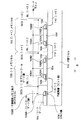
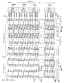
図7(A)は1チップの不揮発性半導体記憶装置の平面レイアウト図であり、ワード線駆動部201を挟んだ左右のメモリセルアレイ領域200A,200Bは、例えば32個のセクタ領域210にそれぞれ分割されている。1チップの不揮発性半導体記憶装置としては、第0〜第63のセクタ領域210を有する。
32個のセクタ領域210は、図7(A)に示すように左右のメモリセルアレイ領域200A,200Bを第2の方向(行方向)Bでそれぞれ分割したもので、各セクタ領域210は第1の方向(列方向)Aを長手方向とする縦長形状を有する。データ消去の最小単位がセクタ領域210であり、セクタ領域210内の記憶データは一括消去される。
【0064】
左右のメモリアレイ領域200A,200Bの各々は、例えば4K本のワード線WLと2K本のビット線BLを有する。ここで、本実施の形態では1本のビット線BLに2つのMONOSメモリセル108A,108Bが接続されるため、2K本のビット線BLは4Kbitの記憶容量を意味する。図7(A)の不揮発性半導体記憶装置は左右のメモリアレイ領域200A,200Bを有するため、メモリ全体として(4K本のワード線WL)×(2K本のビット線BL)×2×2で定義される記憶容量を有する。各セクタ領域210の記憶容量はメモリ全体の記憶容量の1/64であり、(4K本のワード線WL)×(64本のビット線BL)×2で定義される記憶容量を有する。
【0065】
図7(B)は、図7(A)に示す不揮発性半導体記憶装置の一つのセクタ領域210の詳細を示している。図7(B)に示すように、各セクタ領域210は第2の方向にて分割され、16ビットのデータをリード・ライト可能にI/O0〜I/O15用の16個のメモリブロック(入出力ビットに対応したメモリブロック)214を有している。各メモリブロック214は、図7(B)に示すように、4k(4096)本のワード線WLを有する。
【0066】
図7(C)に示すように、図7(B)に示す一つのメモリブロック214は、第1の方向Aにて8個のラージブロック212に分割されている。この各ラージブロック212は、図7(D)に示すように、第1の方向Aにて8個のスモールブロック215に分割されている。
各スモールブロック215は、図7(E)に示すように、64本のワード線WLを有する。
【0067】
よって、一つのラージブロック212に配されるワード線WLの総数(冗長用も含む)は、64本×8スモールブロック=512本となる。このため、一つのセクタ領域210に配されるワード線WLの総数は、512(本)×8(ラージブッロク)=4096本となる。
【0068】
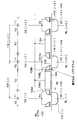
(セクタ領域の詳細)
図8は、図7(A)に示すセクタ領域0の詳細を示している。図8に示すスモールメモリブロック216は、図9に示すように、メモリセル100を列方向に例えば64個、行方向に例えば4個配列したものである。一つのスモールメモリブロック216には、例えば第1層の金属配線層である4本のサブコントロールゲート線SCG0〜SCG3と、データの入出力線である4本のビット線BL0〜BL3と、64本のワード線WLとが接続されている。
【0069】
ここで、偶数のコントロールゲート線SCG0,SCG2には、偶数列(第0列または第2列)の複数メモリセルの各々の第2のコントロールゲート106Bと奇数列(第1列または第3列)の複数メモリセルの各々の第1のコントロールゲート106Aとが共通接続されている。同様に、奇数のサブコントロールゲート線SCG1,SCG3には、奇数列(第1列または第3列)の複数メモリセルの各々の第2のコントロールゲート106Bと偶数列(第2列または第4列)の複数メモリセルの各々の第1のコントロールゲート106Aとが共通接続されている。
【0070】
図8に示すように、スモールメモリブロック216が列方向に64個配列され、16ビットの入出力を行うために、I/O0〜I/O15に対応した16個のスモールメモリブロック216が行方向に配列されている。
【0071】
各スモールメモリブロック216では、コントロールゲート線SCG0が、行方向に延びる例えば第2層の金属配線M0に共通接続されている。同様に、16本のサブコントロールゲート線SCG1は金属配線M1に、16本のサブコントロールゲート線SCG2は金属配線M2に、16本のサブコントロールゲート線SCG3は金属配線M3にそれぞれ共通接続されている。
【0072】
このセクタ領域0のコントロールゲート駆動部である8個のCGドライバ300−0〜300−7が設けられている。CGドライバ300−0から列方向に延びる4本のメインコントロールゲート線MCG00〜MCG03が設けられ、これらは例えば第3層の金属配線により形成されている。同様に、CGドライバ301−0からは4本のメインコントロールゲート線MCG10〜MCG13が、CGドライバ300−2からは4本のメインコントロールゲート線MCG20〜MCG23が、…CGドライバ300−7からは4本のメインコントロールゲート線MCG70〜MCG73が、それぞれ列方向に延びている。
【0073】
ここで、CGドライバ300−0から列方向に延びる4本のメインコントロールゲート線MCG00〜MCG03は、図8に示すようにラージブロック0の領域に亘って延びている。そして、ラージブロック0〜7の各々に配置された8本、計64本の金属配線M0は、メインコントロールゲート線MCG00に共通接続されている。同様に、64本の金属配線M1はメインコントロールゲート線MCG01に、64本の金属配線M2はメインコントロールゲート線MCG02に、64本の金属配線M3はメインコントロールゲート線MCG03にそれぞれ共通接続されている。
【0074】
換言すれば、CGドライバ300−0から列方向に延びる4本のメインコントロールゲート線MCG00〜MCG03は、図8に示すようにラージブロック0内に配置された全メモリセルの第1,第2のコントロールゲート106A,106Bにのみ電位を供給可能で、他のラージブロック1−7には接続されていない。
【0075】
同様に、図8では省略されているが、CGドライバ300−1はラージブロック1と、CGドライバ300−2はラージブロック2と、…CGドライバ300−6はラージブロック6とそれぞれ接続されている。
【0076】
図8ではさらに、CGドライバ300−7がラージブロック7とのみ接続されている状態が図示されている。
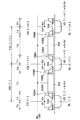
【0077】
図10は、相隣り合うセクタ領域0とセクタ領域1との関係を示している。セクタ領域0とセクタ領域1とはワード線WLが共用されるが、メインコントロールゲート線MCG及びメインビット線MBLはそれぞれ独立して設けられている。特に図10では、セクタ領域0に対応するドライバの一つであるCGドライバ300−0と、セクタ領域1に対応するドライバの一つであるCGドライバ301−0とが示され、CGドライバはセクタ領域毎に独立して設けられている。
【0078】
また、例えばセクタ領域0を例に挙げれば、スモールメモリブロック216毎に配置された複数のサブコントロールゲート線SCG0はメインコントロールゲート線MCG00に共通接続されている。このメインコントロールゲート線MCG00から各サブコントロールゲート線SCG0に至る各経路途中には、ゲート回路は配置されていない。
【0079】
同様に、スモールメモリブロック216毎に配置された複数のビット線BL0(不純物層)は、金属配線であるメインビット線MBL0に共通接続されている。このメインビット線MBL0から各ビット線BL0に至る各経路途中にも、ゲート回路は配置されていない。なお、以上のことは他のセクタ領域1−7についても同様である。
【0080】
(動作説明)
ここで、本実施形態の不揮発性半導体記憶装置でのデータ消去時とプログラム時とについて、設定されるコントロールゲート線CG、ビット線BL及びワード線WLの各電位を、下記の表1に示す。
【0081】
【表1】

表1において、データ消去時には例えばセクタ領域0(選択セクタ)内は全て選択セルとなり、4096本のワード線WLには1.8Vが供給される。また、CGドライバ300−0〜300−7によって32本の全てのメインコントロールゲート線MCG00〜MCG03,MCG10〜MCG13,…MCG70〜MCG73に第1の消去用高電位(例えば−5V)が供給され、セクタ領域0(選択セクタ)内の全メモリセルのコントロールゲート106A,106Bに、一括して第1の消去用高電位を供給することができる。このとき、セクタ領域0内の全ビット線BLには第2の消去用高電位(例えば5V)が供給されるが、その供給方法については後述する。こうして、選択されたセクタ領域0内の全メモリセルにてデータ消去を実施できる。
【0083】
このとき、非選択である例えばセクタ領域1では、4096本の全ワード線WLに1.8Vが供給されるが、コントロールゲートCG及びビット線BLはセクタ領域0とは独立して0Vを供給できるので、非選択セクタにてデータ消去が実施されることはない。
【0084】
次に、プログラミング動作について説明する。選択されたセクタ領域0内の例えばラージブロック0に配置された16個のI/Oにそれぞれ対応する各一つのMONOSメモリセルにて、16ビット同時にデータプログラミングが実施される。このために、セクタ領域0内の選択セルに接続されたいずれか1本のワード線WLに1Vが供給され、他の4095本のワード線WLは0Vに設定される。また、セクタ領域0内のラージブロック0に配置された、各I/O0〜I/O15に対応する16個のメモリブロック214において、図5のCG[i],CG[i+1]に相当する2本のコントロールゲート線CGに5Vを供給し、他のコントロールゲート線CGは0Vに設定する。さらに、セクタ領域0内の各メモリブロック214において、図5のビット線BL[i+1]に相当する1本のビット線BLに5Vを供給し、他のビット線BLは0Vに設定する。これにより、セクタ領域0内のラージブロック0に配置された各メモリブロック214内の各一つのMONOSメモリセルにてデータプログラミングが実施される。
【0085】
このとき、表1に示すように、選択されたセクタ領域0内のラージブロック0に配置された非選択セルにおいては、ワード線WLは0Vに設定されるが、コントロールゲート線CG及びビット線BLには共に5Vの高電位が印加される。
【0086】
一方、表1に示すように、非選択のセクタ領域内における非選択セルにおいては、コントロールゲート線CG及びビット線BLには共に0Vが印加される。よって、非選択セクタ領域内では、プログラム時と同様な高電位が印加されることで生ずるディスターブが非選択セルに生ずることがない。このことは、選択されたセクタ領域0内のラージブロック0を除くラージブロック1−7に配置された非選択セルについても同様である。
【0087】
選択されたセクタ領域0内のラージブロック0に配置された非選択セルには高電位が印加されてしまうが、このような高電位はセクタ領域0内のラージブロック0にてプログラミングを実施する場合にのみ印加される。よって、いずれか一つのセクタ領域でのプログラミングが実施される度に、他のセクタ領域内の非選択セルに高電位が印加されるものと比較すれば、高電位が印加される頻度が大幅に低減し、ディスターブが生ずることを防止できる。
【0088】
(比較例1の説明)
図11は、比較例1の構成を示している。この比較例1では、メモリセルアレイ領域は、列方向で分割され、列方向を長手方向とする複数のセクタ領域0,1,…を有する。また比較例1では、CGドライバ400,401はセクタ領域0,1にそれぞれ対応して設けられずに、両セクタ領域0,1に共用されている。
【0089】
ここで、図11に示すように、セクタ領域0に対応して選択ゲート領域402が、セクタ領域1に対応して選択ゲート領域403がそれぞれ設けられている。選択ゲート領域402,403に配置されたN型MOSトランジスタ群は、選択信号線CGS0,CGS1の電位に基づいて、CGドライバ400,401から供給される電位をセクタ領域0,1に供給するか否かを選択するものである。同様に、選択ゲート領域402,403に配置された他のN型MOSトランジスタ群は、選択信号線BLS0,BLS1の電位に基づいて、セクタ領域0,1のビット線BLの接続/非接続を選択している。
【0090】
図11に示す比較例1の不揮発性半導体記憶装置でのデータ消去時とプログラム時とについて、設定されるコントロールゲート線CG、ビット線BL、ワード線WL及び選択信号線CGS,BLSの各電位を、下記の表2に示す。
【0091】
【表2】
表2に示すように、比較例1においても実質的に表1に示す本実施形態での設定電位と同じ電位に設定できるが、これらは選択ゲート領域402,403を設けることで達成できるのである。もし選択ゲート領域402,403が存在しなければ、選択されたセクタ領域0での選択セルのプログラミング時に、非選択のセクタ領域1の非選択セルにも高電位が印加されてしまう。このようにセクタ領域を越えてプログラム時の高電位が非選択セルにも印加されると、プログラムの度に非選択セルに高電位が印加され、ディスターブが生じてしまう。
【0093】
比較例1では、上記のようなディスターブの発生を防止するために、各セクタ領域毎に選択ゲート領域を設けることが不可欠である。しかし、このような選択ゲート領域の占有スペース分だけ面積が増大し、メモリセルの集積度が低下してしまう。
【0094】
さらに比較例1では、選択ゲート領域402,403にN型MOSトランジスタを使用すると、そこで電圧降下が生ずるため、CGドライバ400,401からは本来必要な第1の消去用高電位に電圧降下分の電圧を上乗せして供給しなければならず、高電圧化してしまう。
【0095】
上述した本発明の実施形態では、ディスターブを回避しながらも選択ゲート領域を省略でき、メモリセルの高集積化と低電圧駆動とが可能となる。
【0096】
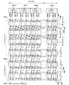
(比較例2)
図15は比較例2の構成を示している。図15においても、本実施の形態と同様なセクタ領域0〜31に分割されている。ただし、例えばセクタ領域0のコントロールゲート駆動部としてCGドライバ300のみが設けられている。このCGドライバ300から列方向に延びる4本のメインコントロールゲート線MCG0〜MCG3が設けられ、これらは例えば第3層の金属配線により形成されている。そして、ラージブロック0〜7の各々に配置された8本、計64本の金属配線M0は、メインコントロールゲート線MCG0に共通接続されている。同様に、64本の金属配線M1はメインコントロールゲート線MCG1に、64本の金属配線M2はメインコントロールゲート線MCG2に、64本の金属配線M3はメインコントロールゲート線MCG3にそれぞれ共通接続されている。
【0097】
図15に示す比較例2においても、セクタ領域0内にデータのプログラミングを実施している時には、他のセクタ領域1−31ではメモリセルに高電位を印加しなくて済み、しかも選択ゲート領域を設けずともディスターブを防止することができる。ただし、比較例2ではセクタ領域0のいずれかのメモリセルについてデータプログラミングを実施している時には、このセクタ領域0内の全てのメモリセルに高電位が等しく印加されることになり、この点で本実施の形態よりも劣っている。
【0098】
比較例2ではさらに、メインコントロールゲート線MCG0〜MCG3の各々に対して、ラージブロック0〜7に亘る列方向の全てのメモリセルが接続される。
よって、本実施の形態のようにメインコントロールゲート線がいずれか一つのラージブロック内のメモリセルに接続されるものと比較すれば、本実施の形態のメインコントロールゲート線に接続される負荷容量(ゲート容量)は比較例2の1/8となる。
【0099】
高電位が供給されるメインコントールゲート線に接続される負荷容量が大きいと、メインコントロールゲート線をその高電位に充電するまでに要する時間が長くなり、高速駆動が不可能となるが、本実施の形態はその点で比較例2よりも優れている。
【0100】
なお、図10に示す本発明の実施形態においては、ビット線BLについては選択ゲートを追加することも可能である。このようにして、選択されたセクタ0中の非選択セルについては、ビット線BLを選択ゲートによってフローティング状態としても良い。こうすると、プログラムが選択されたセクタ領域0内の非選択セルのビット線BLは、高電位とならない。よって、非選択セルでのデータのディスターブはさらに低減できる。なお、選択ゲートを介してビット線に高電位を供給する時には、電圧降下が生ずるおそれは残る。
【0101】
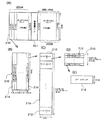
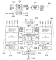
(1チップメモリの構成)
図12は、上述の不揮発性半導体記憶装置を1チップ化したときの概略ブロック図である。図12において、このICチップ500には、左アレイブロック502及び右アレイブロック504が設けられている。この左右のアレイブロック502,504の各々は、図7にて説明したメモリセルアレイ領域を含んでいる。
【0102】
この左右のアレイブロック502,504の間には、CGデコーダ506、Xプリデコーダ508、WLドライバ(左)510、WLドライバ(右)512及びYでコーダ514が配置されている。
【0103】
左右のメモリブロック502,504には、センスアンプ/BLドライバ516,518がそれぞれ接続されている。このセンスアンプ/BLドライバ516,518のいずれか一方に対して、16ビットの信号IO0−15が、データイン/アウトバッファ520及び入出力端子522を介して入出力される。
【0104】
ICチップ500にはさらに、コマンド端子530を介して入力される各種イネーブル信号に基づいて、制御ロジック信号を生成する制御ロジック回路532が設けられている。この制御ロジック回路532からの出力に基づいて、コントロールゲート線WL及びビット線BLなどに供給される各種電位が電位生成回路534にて生成される。
【0105】
一方、アドレス端子640を介して外部から入力されるアドレス信号ADR[0−20]に基づいて、アドレスバッファ542にて内部アドレス信号A0−20が生成される。この内部アドレス信号A0−20の定義を下記の表3に示す。
【0106】
【表3】
表3に示すように、内部アドレス信号の上位6ビットA[20:15]は、図7(A)に示すセクタ領域0−63の一つを選択するのに用いられる。内部アドレス信号の中位3ビットA[14:12]は、図9に示す一つのスモールメモリブロック216の中から8ビットのうちの一つを選択するのに用いられる。内部アドレス信号の下位12ビットA[11:0]は、4096本のワード線WLの一本を選択するために用いられる。
【0108】
図13は、図12に示す左メモリブロック502の詳細を示している。このメモリブロック502は、図7(A)と同様に32分割されたセクタ領域0−31を有し、セクタ領域0−31の各々には図7(B)と同様に8つのラージブロック0−7が設けられている。
【0109】
図13に示すように、32個のセクタ領域の各一つと対応してCGドライバ300〜331が設けられている。セクタ領域0に対応するCGドライバ300は、図8に示したものと同じであり、ラージブロック0−8から成るセクタ領域0内の各メモリセルにコントロールゲート電位を直接供給するものである。他のCGドライバ301〜331も同様の機能を有する。
【0110】
図13において、32個のセクタ領域0−31の各一つに対応して、消去用ビット線駆動部であるウェルドライバ340−0〜340−31が設けられている。ウェルドライバ340−0は、セクタ領域0内の例えばP型ウェルに第2の消去用高電位を供給して、第2の消去用高電位に設定するものである。他のウェルドライバ340−1〜340−31も同様の機能を有する。
【0111】
図13において、32個のセクタ領域0−31の各一つに対応して、セクタデコーダ350−0〜350−31が設けられている。セクタデコーダ350−0は、内部アドレス信号の上位6ビットA[20:15]にて生成される信号をデコードする。そして、セクタ0が選択された際には、セクタデコード350−0がCGドライバ300、ウェルドライバ340−0を駆動して、必要な電位がコントロールゲート線CG、ビット線BLに供給されるようにする。
【0112】
図13において、32個のセクタ領域0−31の各一つに対応して、Yパス回路360−0〜360−31と、セクタ選択回路370−0〜370−31が設けられている。Yパス回路360−0〜360−31は、図12に示すYデコーダ514からの信号に基づいて、16個の各I/Oに接続されたビット線BL0−3の一本を選択する。セクタ選択回路370−0〜370−31は、対応するセクタデコーダ360−0〜360−31からの選択信号SEC0〜SEC31に基づいて、図12に示すセンスアンプ/BLドライバ516との接続/非接続を行う。
【0113】
なお、本発明は上述した実施の形態に限定されるものではなく、本発明の要旨の範囲内で種々の変形実施が可能である。
【0114】
例えば、不揮発性メモリ素子108A,108Bの構造については、MONOS構造に限定されるものではない。1つのワードゲート104と第1,第2のコントロールゲート106A,106Bにより、2箇所にて独立して電荷をトラップできる他の種々のメモリセルを用いた不揮発性半導体記憶装置に、本発明を適用することができる。
【0115】
また、上述の実施形態では、セクタ領域の分割数、ラージブロック、スモールブロックの分割数については一例であり、他の種々の変形実施が可能である。すなみに、ラージブロックの分割数を8としたのはメタル配線ピッチの制約から決められた。もしメタル配線ピッチを狭く出来れば、分割数をさらに増やすことができる。例えば16分割にすれば、1本のコントロールゲート線の負荷容量(ゲート容量)はさらに減るので、より高速駆動が可能となる。ただし、16分割とするとメインコントロールゲート線の数が増えるので、ライン&スペースを狭くするか、面積を増大させるしかない。また、コントロールゲートドライバの数も増えるので、その分面積が増大する。
【0116】
図14は、図8に示すスモールメモリブロック216に対する配線の変形例を示している。図14では、CGドライバ300−0からのメインコントロールゲート線MCG00〜MCG03は、図8のようにラージブロック0内の全てのスモールブロック0−7に接続されるのでなく、ラージブロック0〜7の各スモールブロック0にのみ接続されている。CGドライバ300−1は、ラージブロック0〜7の各スモールブロック2にのみ接続されている。CGドライバ300−7は、ラージブロック0〜7の各スモールブロック7のみに接続されている。
【0117】
図14に示す接続形態であっても、図8に示す接続形態と同様な作用・効果を奏することができる。
【図面の簡単な説明】
【図1】本発明の一実施の形態に係る不揮発性半導体記憶装置に用いられるメモリセルの断面図である。
【図2】図1に示すメモリセルの等価回路図である。
【図3】図1に示す不揮発性半導体記憶装置でのデータ読み出し動作を説明するための概略説明図である。
【図4】図1に示すメモリセルでのコントロールゲート電圧VCGとソース−ドレイン電流Idsとの関係を示す特性図である。
【図5】図1に示す不揮発性半導体記憶装置でのデータ書き込み(プログラム)動作を説明するための概略説明図である。
【図6】図1に示す不揮発性半導体記憶装置でのデータ消去動作を説明するための概略説明図である。
【図7】図7(A)は図1に示す不揮発性半導体記憶装置全体の平面レイアウト図、図7(B)は図7(A)中の一つのセクタ領域の平面図、図7(C)は図7(B)中の一つのメモリブロックの平面図、図7(D)は図7(C)中の一つのラージブロックの平面図、図7(E)は図7(D)中の一つのスモールブロックの平面図である。
【図8】図7(B)に示す一つのセクタ領域の多数のメモリブロックとその配線とを説明するための概略説明図である。
【図9】図8に示すスモールメモリブロックの詳細を示す回路図である。
【図10】隣り合うセクタ領域の関係を示す回路図である。
【図11】図10に対する比較例1の構成を示す回路である。
【図12】1チップ化された不揮発性半導体記憶装置のブロック図である。
【図13】図12に示す左メモリブロックの詳細を示すブロック図である。
【図14】一つのセクタ領域内のスモールメモリブロックに対する配線を図8とは異ならせた変形例を説明するための概略説明図である。
【図15】図8及び図14とはさらに異なる配線とした比較例2の構成を説明するための概略説明図である。
【符号の説明】
100 メモリセル
102 P型ウェル
104 ワードゲート
106A,106B コントロールゲート(線)
108A,108B 不揮発性メモリ素子(MONOSメモリセル)
109 ONO膜
110 不純物層(ビット線)
200A,200B メモリセルアレイ領域
201 ワード線駆動部
210 セクタ領域
212 ラージブロック
214 メモリブロック
215 スモールブロック
216 スモールメモリブロック
300−0〜331−7 CG(コントロールゲート)ドライバ
340−0〜340−31 ウェルドライバ(消去用ビット線駆動部)
350−0〜350−31 セクタドライバ
360−0〜360−31 Yパス回路
370−0〜370−31 セクタ選択回路
400,401 CG(コントロールゲート)ドライバ
402,403 選択ゲート領域
500 ICチップ
502,504 アレイブロック
506 CGデコーダ
508 Xプリデコーダ
510,512 WL(ワード線)ドライバ
514 Yデコーダ
516,518 センスアンプ/BLドライバ
520 データイン/アウトバッファ
522 入出力端子
530 コマンド端子
532 制御ロジック回路
534 電位生成回路
540 アドレス端子
542 アドレスバッファ
WL ワード線
BL ビット線(不純物層)
MBL メインビット線
SCG サブコントロールゲート線(第1層金属配線)
M0〜M3 第2層金属配線
MCG メインコントロールゲート線(第3層金属配線)[0001]
BACKGROUND OF THE INVENTION
The present invention relates to a nonvolatile semiconductor memory device including a memory cell including one word gate and two nonvolatile memory elements controlled by two control gates.
[0002]
[Background]
As a nonvolatile semiconductor device, a gate insulating layer between a channel and a gate is formed of a stacked body of a silicon oxide film, a silicon nitride film, and a silicon oxide film, and MONOS (Metal-Oxide-) in which charges are trapped in the silicon nitride film. Nitride-Oxide-Semiconductor or -substrate) type is known.
[0003]
This MONOS type nonvolatile semiconductor memory device is disclosed in a literature (Y. Hayashi, et al, 2000 Symposium on VLSI Technology Digest of Technical Papers p.122-p.123). This document discloses a twin MONOS flash memory cell including one word gate and two nonvolatile memory elements (MONOS memory cells) controlled by two control gates. That is, one flash memory cell has two charge trap sites.
[0004]
A plurality of twin MONOS flash memory cells having such a structure are arranged in the row direction and the column direction to constitute a memory cell array region.
[0005]
[Problems to be solved by the invention]
Driving the twin MONOS flash memory cell requires two bit lines, one word line, and two control gate lines. However, when driving a large number of memory cells, even if different control gates are set to the same potential, these lines can be connected in common.
[0006]
Here, the operation of the flash memory includes data erasing, programming, and reading. Data programming and reading are usually performed simultaneously in 8-bit or 16-bit selected cells, but data erasing can be performed simultaneously in a wider range.
[0007]
Here, in this type of nonvolatile memory, disturbing data has become a problem. Data disturb means that when a high potential is applied to the control gate line and bit line of a selected cell to perform programming or erasing, a high potential is also applied to a cell in a non-selected sector region by a shared wiring, It means that the data is not disturbed by programming or erasing by repeating the state every time the program is performed.
[0008]
In order to prevent such a situation, it is possible to provide a selection gate circuit so that a high potential is applied only to the cells in the selected sector and no high potential is applied to the cells in the non-selected sector.
[0009]
However, in this case, an area is occupied for the selection gate circuit, and high integration of the memory cells is hindered. Furthermore, when a voltage drop occurs in the selection gate, it is necessary to supply an additional voltage drop in order to supply a high potential to the cells in the selected sector during programming or erasing. As a result, low-voltage driving is hindered, and in particular, it is incompatible with devices that require low power consumption, such as portable devices.
[0010]
Further, in the future, there will be a demand for reading data at high speed from portable devices, but there is room for improvement in terms of high-speed driving.
[0011]
Therefore, the present invention is a non-volatile memory that can avoid high data density without a selection gate circuit while avoiding data disturbance in a cell in an unselected sector during programming or erasing in a selected cell. A semiconductor memory device is provided.
[0012]
Another object of the present invention is to provide a nonvolatile semiconductor device that can reduce a power consumption by avoiding a voltage drop by eliminating a selection gate circuit.
[0013]
Still another object of the present invention is to provide a non-volatile semiconductor memory device capable of high-speed driving by reducing the load capacity of a control gate line to which a high potential is supplied.
[0014]
[Means for Solving the Problems]
A nonvolatile semiconductor memory device according to one embodiment of the present invention includes a memory cell including two nonvolatile memory elements controlled by one word gate and two control gates. Column direction and row direction Each have a plurality of memory cell array regions. The nonvolatile semiconductor memory device further includes a control gate driver that drives the first and second control gates of each of the plurality of memory cells in the memory cell array region.
[0015]
The memory cell array region has a plurality of sector regions divided in the row direction. Each of the plurality of sector areas is line A plurality of memory cells are arranged in each of a plurality of columns along the direction.
[0016]
Each of the plurality of sector areas Column It has a plurality of blocks divided into a plurality in the direction. The control gate driver has a plurality of control gate drivers for each of the plurality of sector regions. Each of the plurality of control drivers sets the potentials of the first and second control gates of all the memory cells arranged in one or more different blocks among the plurality of blocks.
[0017]
According to an aspect of the present invention, when programming a selected cell arranged in one block in one sector area, a memory cell (selected in the selected block in the sector area) is selected. Only the control gate potential of the cell and the non-selected cell can be set as the program potential by the corresponding control gate driver. Other blocks in the selected sector and non-selected sector areas can be set to potentials other than the program potential by the corresponding control gate driver, so that data is disturbed in non-selected cells in the non-selected sector area. There is no. In addition, since this can be achieved without using the selection gate circuit, the memory cells can be highly integrated. In addition, since no voltage drop occurs in the selection gate circuit, low voltage driving is possible, and it can be used effectively as a memory for portable devices. Furthermore, since only one memory cell in one block is connected to one control gate driver, it is connected to the control gate line as compared with the case in which all memory cells in one sector region are connected. The load capacity (gate capacity) is reduced. Therefore, the memory can be driven at a high speed.
[0018]
As multiple blocks, Column A plurality of large blocks divided into a plurality of directions and each of the large blocks Column It can have a plurality of small blocks that are further subdivided in direction.
[0019]
In this case, each of the plurality of control drivers is arranged in a different one of the plurality of large blocks, and the potentials of the first and second control gates of all the memory cells arranged in the plurality of small blocks. Can be set.
[0020]
Alternatively, each of the plurality of control drivers can set the potentials of the first and second control gates of all the memory cells arranged in one different small block for each of the plurality of large blocks.
[0021]
In one embodiment of the present invention, one of a plurality of control gate drivers is selected at the time of data erasing, and the first erasing high potential is supplied to all the first and second control gates in the one sector region. be able to. In this way, data erasure can be performed collectively in each of the plurality of sector areas.
[0022]
In one embodiment of the present invention, each of the plurality of sector regions includes Column A plurality of control gate lines formed along the direction are provided, and the control gate driver is directly connected to each of the plurality of control gate lines arranged in each of the plurality of sector regions without passing through the gate circuit. It is preferable that
[0023]
Thus, even if the gate circuit that increases the area and causes a voltage drop is eliminated, a high potential is not applied to the non-selected cells in the non-selected sector region.
[0024]
Here, the plurality of control gate lines include a plurality of main control gate lines directly connected to the control gate driver, a plurality of main control gate lines, and the first and second control gates of the plurality of memory cells. And a plurality of sub-control gate lines for connecting to each other. These can be formed by metal wirings having different layers.
[0025]
At this time, the even-numbered main control gate lines provided in each of the plurality of sector regions include the second control gate of each of the even-numbered memory cells and the first control of each of the odd-numbered memory cells. A plurality of sub-control gates that are commonly connected to the gate can be connected. On the other hand, an odd number of main control gate lines provided in each of the plurality of sector regions include a second control gate of each of the odd-numbered memory cells and a first control gate of each of the even-numbered memory cells. Can be connected to a plurality of sub-control gate lines.
[0026]
Further, when k main control gate lines are connected to each of the plurality of control gate drivers provided corresponding to each of the plurality of sector regions, each of the plurality of sector regions has k pieces A memory block corresponding to each input / output bit composed of a memory cell group to which the sub-control gate line is connected, line A plurality are arranged in the direction. At this time, line It is preferable to provide a plurality of wirings extending along the direction. Thus, each of the k main control gate lines can be connected to each of the k sub control gate lines corresponding thereto via one of the plurality of wirings.
[0027]
As a particularly preferable form, the memory block line The number of memory cells along the direction can be four. In this case, k = 4 is set, and four main control gate lines are connected to the control gate driver. Memory block line Since there are four cells in the direction, the total is 8 bits, and one sub control gate line is shared by 2 bits, so that four sub control gate lines are arranged.
[0028]
In one aspect of the present invention, each of the plurality of sector regions includes Column It can further include a plurality of bit lines formed along the direction and a bit line driver for driving the plurality of bit lines at least during data programming and reading.
[0029]
The bit line driving unit may drive a plurality of bit lines at the time of erasing data, but an erasing bit line driving unit may be further provided. The erasing bit line driving unit supplies a second erasing high potential to a plurality of bit lines formed in one sector area at the time of erasing data for each sector area.
[0030]
Each of the plurality of sector regions can be formed in one well region separated from other sectors. In this case, an erasing well driver for supplying the second erasing high potential can be provided in the well region.
[0031]
In addition, a plurality of bit lines are formed with an impurity layer. But Each of the plurality of bit lines may be connected to each of the plurality of main bit lines. If the main bit line is a metal wiring, the resistance of the bit line can be reduced and the impurity layer can be reduced. Column Even if it is discontinuous without being continuous in the direction, power can be supplied to each discontinuous bit line via the main bit line.
[0032]
At this time, it is preferable that no gate circuit is provided in the middle of a path from the plurality of main bit lines to the plurality of bit lines. This is because the gate circuit increases the wiring capacity of the bit line and may cause a voltage drop in the gate circuit, which hinders low voltage driving.
[0033]
In the memory cell array area, line A plurality of words commonly connected to the word gates of each of the plurality of memory cells arranged along the direction; line It can be provided along the direction. Thus, multiple sector areas In A plurality of word lines are shared. In the memory cell array region line A word line driver for driving a plurality of word lines can be provided at one end in the direction. To further increase the storage capacity of the nonvolatile semiconductor memory device, line A plurality of memory cell array regions may be arranged on both sides of the word line driver in the direction.
[0034]
Each of the first and second nonvolatile memory elements includes an oxide film (O), a nitride film (N), and an oxide film (O). Or However, the present invention is not limited to this, and other structures can be adopted.
[0035]
DETAILED DESCRIPTION OF THE INVENTION
Embodiments of the present invention will be described below with reference to the drawings.
[0036]
(Memory cell structure)
FIG. 1 shows a cross section of a nonvolatile semiconductor memory device, and FIG. 2 is an equivalent circuit diagram thereof. In FIG. 1, one
[0037]
The first and
[0038]
Each of the first and
[0039]
Thus, one
[0040]
The first and second
As shown in FIGS. 1 and 2, the plurality of
[0041]
Further, the
[0042]
Here, the
[0043]
In the P-type well 102, the [i + 1] th memory cell 100B of the [i] th memory cell 100 [i] and the
[0044]
These impurity layers 110 [i], [i + 1], and [i + 2] are n-type impurity layers formed in, for example, a P-type well, and are arranged in the column direction (first direction A direction perpendicular to the paper surface of FIG. 1). A bit line that extends along the column and is shared by the plurality of
[0045]
(Reading data from memory cells)
In one
[0046]
In describing the operation of the
[0047]
In this case, for example, 2.5 V is applied to each
[0048]
At this time, the operation of the transistor T3 corresponding to the
[0049]
FIG. 4 shows the relationship between the voltage applied to the
[0050]
As shown in FIG. 4, when no charge is accumulated in the
[0051]
Here, the voltage Vread applied to the
[0052]
Therefore, the current Ids flows when no charge is accumulated in the
[0053]
Here, when reading data, the potential VD [i] of the bit line BL [i] (impurity layer 110 [i]) is set to 0V, and the potential VD [i + 1] of the bit line BL [i + 1] (impurity layer 110 [i + 1]). Are set to 1.5V respectively. As a result, when no charge is accumulated in the
[0054]
In the memory cell 100 [i + 1], the transistors T1 and T2 are turned on, but the control gate potential VCG of the transistor T3 is set to 0 V, and the potential VCG is obtained from both the two threshold voltages Vlow and Vhigh in FIG. Since it is low, source-drain current does not flow in the memory cell 100 [i + 1]. Therefore, the data accumulation state in the memory cell 100 [i + 1] does not adversely affect the data reading from the memory cell 100 [i].
[0055]
In order to read data from the
[0056]
(Programming memory cells)
FIG. 5 is a diagram illustrating data programming of the
[0057]
In FIG. 5, as in FIG. 3, the potential of the sub control gate line SCG [i] is set to an override potential (for example, 5V), and the potential of the sub control gate line SCG [i + 2] is set to 0V. However, the potential of each
[0058]
Thus, the transistors T1 and T2 of the memory cell 100 [i] are turned on, and the current Ids flows toward the impurity layer 110 [i]. On the other hand, channel hot electrons (in the
[0059]
(Erase memory cell data)
FIG. 6 is a diagram for explaining data erasure of two memory cells 100 [i] and [i + 1] connected to the word line WL.
[0060]
In FIG. 6, the potential of each
[0061]
In this way, the electrons trapped in the
[0062]
(Overall configuration of nonvolatile semiconductor memory device)
The entire configuration of the nonvolatile semiconductor memory device configured using the above-described
[0063]
FIG. 7A is a plan layout diagram of a one-chip nonvolatile semiconductor memory device. The left and right memory
As shown in FIG. 7A, the 32
[0064]
Each of the left and right
[0065]
FIG. 7B shows details of one
[0066]
As shown in FIG. 7C, one
Each
[0067]
Therefore, the total number (including redundancy) of word lines WL arranged in one
[0068]
(Details of sector area)
FIG. 8 shows details of the
[0069]
Here, the even-numbered control gate lines SCG0 and SCG2 include a
[0070]
As shown in FIG. 8, 64 small memory blocks 216 are arranged in the column direction, and in order to perform 16-bit input / output, 16 small memory blocks 216 corresponding to I / O0 to I / O15 are arranged in the row direction. Is arranged.
[0071]
In each
[0072]
Eight CG drivers 300-0 to 300-7 that are control gate driving units in the
[0073]
Here, the four main control gate lines MCG00 to MCG03 extending in the column direction from the CG driver 300-0 extend over the area of the
[0074]
In other words, the four main control gate lines MCG00 to MCG03 extending in the column direction from the CG driver 300-0 are connected to the first and second memory cells arranged in the
[0075]
Similarly, although omitted in FIG. 8, the CG driver 300-1 is connected to the
[0076]
FIG. 8 further shows a state where the CG driver 300-7 is connected only to the
[0077]
FIG. 10 shows the relationship between
[0078]
For example, taking the
[0079]
Similarly, a plurality of bit lines BL0 (impurity layer) arranged for each
[0080]
(Description of operation)
Table 1 below shows the potentials of the control gate line CG, the bit line BL, and the word line WL that are set for data erasing and programming in the nonvolatile semiconductor memory device of this embodiment.
[0081]
[Table 1]
In Table 1, when data is erased, for example, all the sector areas 0 (selected sectors) are selected cells, and 1.8V is supplied to 4096 word lines WL. The first erasing high potential (for example, −5 V) is supplied to all 32 main control gate lines MCG00 to MCG03, MCG10 to MCG13,... MCG70 to MCG73 by the CG drivers 300-0 to 300-7. The first erasing high potential can be collectively supplied to the
[0083]
At this time, in the
[0084]
Next, a programming operation will be described. For example, 16 bits of data programming is simultaneously performed in each MONOS memory cell corresponding to each of 16 I / Os arranged in, for example, the
[0085]
At this time, as shown in Table 1, in the non-selected cells arranged in the
[0086]
On the other hand, as shown in Table 1, in the non-selected cell in the non-selected sector region, 0 V is applied to both the control gate line CG and the bit line BL. Therefore, in the non-selected sector area, a disturbance caused by applying the same high potential as that at the time of programming does not occur in the non-selected cell. The same applies to the unselected cells arranged in the large blocks 1-7 excluding the
[0087]
A high potential is applied to the non-selected cells arranged in the
[0088]
(Description of Comparative Example 1)
FIG. 11 shows the configuration of Comparative Example 1. In Comparative Example 1, the memory cell array region is divided in the column direction, and has a plurality of
[0089]
Here, as shown in FIG. 11, a
[0090]
Each potential of the control gate line CG, the bit line BL, the word line WL, and the selection signal lines CGS and BLS set for data erasing and programming in the nonvolatile semiconductor memory device of Comparative Example 1 shown in FIG. The results are shown in Table 2 below.
[0091]
[Table 2]
As shown in Table 2, the comparative example 1 can be set to substantially the same potential as the set potential in the present embodiment shown in Table 1, but these can be achieved by providing the
[0093]
In the first comparative example, it is indispensable to provide a selection gate region for each sector region in order to prevent the above-described disturbance. However, the area increases by the space occupied by such a select gate region, and the degree of integration of the memory cells decreases.
[0094]
Further, in the first comparative example, when an N-type MOS transistor is used for the
[0095]
In the embodiment of the present invention described above, the selection gate region can be omitted while avoiding disturbance, and the memory cell can be highly integrated and driven at a low voltage.
[0096]
(Comparative Example 2)
FIG. 15 shows the configuration of Comparative Example 2. Also in FIG. 15, it is divided into
[0097]
Also in the comparative example 2 shown in FIG. 15, when data programming is performed in the
[0098]
In Comparative Example 2, all the memory cells in the column direction extending over the
Therefore, as compared with the case where the main control gate line is connected to the memory cell in any one large block as in the present embodiment, the load capacitance connected to the main control gate line of this embodiment ( The gate capacity) is 1/8 that of Comparative Example 2.
[0099]
If the load capacitance connected to the main control gate line to which a high potential is supplied is large, the time required to charge the main control gate line to the high potential becomes long and high-speed driving becomes impossible. Is superior to Comparative Example 2 in that respect.
[0100]
In the embodiment of the present invention shown in FIG. 10, a selection gate can be added for the bit line BL. In this way, for the non-selected cell in the selected
[0101]
(Configuration of 1-chip memory)
FIG. 12 is a schematic block diagram when the above-described nonvolatile semiconductor memory device is made into one chip. In FIG. 12, the
[0102]
Between the left and right array blocks 502 and 504, a
[0103]
Sense amplifier /
[0104]
The
[0105]
On the other hand, the internal address signal A0-20 is generated in the
[0106]
[Table 3]
As shown in Table 3, the upper 6 bits A [20:15] of the internal address signal are used to select one of the
[0108]
FIG. 13 shows details of the
[0109]
As shown in FIG. 13, CG drivers 300 to 331 are provided corresponding to each of the 32 sector areas. The CG driver 300 corresponding to the
[0110]
In FIG. 13, well drivers 340-0 to 340-31 which are erasing bit line driving units are provided corresponding to each of 32 sector regions 0-31. The well driver 340-0 supplies the second erasing high potential to, for example, a P-type well in the
[0111]
In FIG. 13, sector decoders 350-0 to 350-31 are provided corresponding to each of 32 sector regions 0-31. The sector decoder 350-0 decodes the signal generated by the upper 6 bits A [20:15] of the internal address signal. When
[0112]
In FIG. 13, Y path circuits 360-0 to 360-31 and sector selection circuits 370-0 to 370-31 are provided corresponding to each of 32 sector regions 0-31. The Y path circuits 360-0 to 360-31 select one of the bit lines BL0-3 connected to each of the 16 I / Os based on the signal from the
[0113]
The present invention is not limited to the above-described embodiment, and various modifications can be made within the scope of the gist of the present invention.
[0114]
For example, the structure of the
[0115]
In the above-described embodiment, the division number of the sector area, the division number of the large block, and the small block are examples, and other various modifications can be implemented. In fact, the reason why the number of large block divisions was set to 8 was determined by the restriction of the metal wiring pitch. If the metal wiring pitch can be reduced, the number of divisions can be further increased. For example, if it is divided into 16, the load capacity (gate capacity) of one control gate line is further reduced, so that higher speed driving is possible. However, if it is divided into 16, the number of main control gate lines increases, so the line and space can only be narrowed or the area can be increased. In addition, since the number of control gate drivers increases, the area increases accordingly.
[0116]
FIG. 14 shows a modification of the wiring for the
[0117]
Even with the connection configuration shown in FIG. 14, the same operations and effects as the connection configuration shown in FIG. 8 can be achieved.
[Brief description of the drawings]
FIG. 1 is a cross-sectional view of a memory cell used in a nonvolatile semiconductor memory device according to an embodiment of the present invention.
FIG. 2 is an equivalent circuit diagram of the memory cell shown in FIG.
FIG. 3 is a schematic explanatory diagram for explaining a data read operation in the nonvolatile semiconductor memory device shown in FIG. 1;
4 is a characteristic diagram showing a relationship between a control gate voltage VCG and a source-drain current Ids in the memory cell shown in FIG.
FIG. 5 is a schematic explanatory diagram for explaining a data write (program) operation in the nonvolatile semiconductor memory device shown in FIG. 1;
6 is a schematic explanatory diagram for explaining a data erasing operation in the nonvolatile semiconductor memory device shown in FIG. 1. FIG.
7A is a plan layout view of the entire nonvolatile semiconductor memory device shown in FIG. 1, FIG. 7B is a plan view of one sector region in FIG. 7A, and FIG. ) Is a plan view of one memory block in FIG. 7B, FIG. 7D is a plan view of one large block in FIG. 7C, and FIG. 7E is in FIG. 7D. It is a top view of one small block.
FIG. 8 is a schematic explanatory diagram for explaining a large number of memory blocks and wirings in one sector area shown in FIG. 7B;
FIG. 9 is a circuit diagram showing details of the small memory block shown in FIG. 8;
FIG. 10 is a circuit diagram showing a relationship between adjacent sector regions.
11 is a circuit showing a configuration of Comparative Example 1 with respect to FIG.
FIG. 12 is a block diagram of a nonvolatile semiconductor memory device made into one chip.
13 is a block diagram showing details of a left memory block shown in FIG. 12. FIG.
FIG. 14 is a schematic explanatory diagram for explaining a modified example in which wiring for a small memory block in one sector area is different from that in FIG. 8;
FIG. 15 is a schematic explanatory diagram for explaining the configuration of Comparative Example 2 in which the wiring is further different from that of FIGS. 8 and 14;
[Explanation of symbols]
100 memory cells
102 P-type well
104 word gate
106A, 106B Control gate (line)
108A, 108B Non-volatile memory element (MONOS memory cell)
109 ONO film
110 Impurity layer (bit line)
200A, 200B Memory cell array area
201 Word line driver
210 Sector area
212 Large Block
214 memory blocks
215 Small block
216 Small memory block
300-0 to 331-7 CG (control gate) driver
340-0 to 340-31 well driver (erase bit line drive unit)
350-0 to 350-31 Sector driver
360-0 to 360-31 Y-pass circuit
370-0 to 370-31 sector selection circuit
400, 401 CG (control gate) driver
402, 403 Selection gate region
500 IC chip
502,504 array block
506 CG decoder
508 X predecoder
510, 512 WL (word line) driver
514 Y decoder
516,518 sense amplifier / BL driver
520 Data in / out buffer
522 I / O terminal
530 Command terminal
532 Control logic circuit
534 Potential generation circuit
540 Address terminal
542 Address buffer
WL Word line
BL bit line (impurity layer)
MBL main bit line
SCG Sub-control gate line (first layer metal wiring)
M0 to M3 Second layer metal wiring
MCG Main control gate line (3rd layer metal wiring)
Claims (16)
前記メモリセルアレイ領域内の前記複数のメモリセルの各々の前記第1,第2のコントロールゲートを駆動するコントロールゲート駆動部と、
を有し、
前記メモリセルアレイ領域は、前記行方向で分割された複数のセクタ領域を有し、
前記複数のセクタ領域の各々は、前記行方向で複数に分割された複数のブロックを有し、
前記コントロールゲート駆動部は、前記複数のセクタ領域の各一つについてそれぞれ複数のコントロールゲートドライバを有し、前記複数のコントロールドライバの各々は、前記複数のブロックのうち1以上のブロックに対応して配置され、かつ、対応ブロック内の全メモリセルの前記第1及び第2のコントロールゲートの電位を設定することを特徴とする不揮発性半導体記憶装置。A memory cell array region in which a plurality of memory cells each having one word gate and first and second nonvolatile memory elements controlled by first and second control gates are arranged in the column direction and the row direction, respectively. When,
A control gate driver for driving the first and second control gates of each of the plurality of memory cells in the memory cell array region;
Have
The memory cell array region has a plurality of sector regions divided in the row direction,
Each of the plurality of sector regions has a plurality of blocks divided into a plurality in the row direction,
The control gate driving unit has a plurality of control gate drivers for each of the plurality of sector regions, and each of the plurality of control drivers corresponds to one or more blocks of the plurality of blocks. A nonvolatile semiconductor memory device that is arranged and sets potentials of the first and second control gates of all memory cells in a corresponding block.
前記複数のブロックは、前記列方向で複数に分割された複数のラージブロックと、前記複数のラージブロックの各々を前記列方向でさらに細分割された複数のスモールブロックを有し、
前記複数のコントロールドライバの各々は、前記複数のラージブロックの各々に対応して配置され、かつ対応するラージブロックに設けられた前記複数のスモールブロック内に配置された全メモリセルの前記第1及び第2のコントロールゲートの電位を設定することを特徴とする不揮発性半導体記憶装置。In claim 1,
The plurality of blocks include a plurality of large blocks divided into a plurality of rows in the column direction, and a plurality of small blocks each of the plurality of large blocks further subdivided in the column direction,
Each of the plurality of control drivers is arranged corresponding to each of the plurality of large blocks, and the first and all of the memory cells arranged in the plurality of small blocks provided in the corresponding large block. A non-volatile semiconductor memory device, wherein a potential of a second control gate is set.
前記複数のブロックは、前記列方向で複数に分割された複数のラージブロックと、前記複数のラージブロックの各々を前記列方向でさらに細分割された複数のスモールブロックを有し、
前記複数のコントロールドライバの各々は、前記複数のラージブロックの各々に設けられた前記複数のスモールブロックの各々に対応して設けられ、かつ、対応するスモールブロックに配置された全メモリセルの前記第1及び第2のコントロールゲートの電位を設定することを特徴とする不揮発性半導体記憶装置。In claim 1,
The plurality of blocks include a plurality of large blocks divided into a plurality of rows in the column direction, and a plurality of small blocks each of the plurality of large blocks further subdivided in the column direction,
Each of the plurality of control drivers is provided corresponding to each of the plurality of small blocks provided in each of the plurality of large blocks, and each of the plurality of memory cells arranged in the corresponding small block. A non-volatile semiconductor memory device, wherein the potentials of the first and second control gates are set.
前記複数のコントロールゲートドライバは、一つのセクタ領域内のデータ消去時に、該一つのセクタ領域内の全ての前記第1,第2のコントロールゲートに第1の消去用高電位を供給して、前記複数のセクタ領域の各々にて一括してデータを消去することを特徴とする不揮発性半導体記憶装置。In any one of Claims 1 thru | or 3,
The plurality of control gate drivers supply a first erasing high potential to all the first and second control gates in one sector area when erasing data in one sector area, and A non-volatile semiconductor memory device, wherein data is erased collectively in each of a plurality of sector areas.
前記複数のセクタ領域の各々には、前記列方向に沿って形成された複数のコントロールゲート線が設けられ、
前記コントロールゲート駆動部は、前記複数のセクタ領域の各々に配置された前記複数のコントロールゲート線の各々に、ゲート回路を経由せずに直接接続されていることを特徴とする不揮発性半導体記憶装置。In claim 4,
Each of the plurality of sector regions is provided with a plurality of control gate lines formed along the column direction,
The control gate driving unit is directly connected to each of the plurality of control gate lines arranged in each of the plurality of sector regions without going through a gate circuit. .
前記複数のコントロールゲート線は、
前記コントロールゲート駆動部に直接接続された複数のメインコントロールゲート線と、
前記複数のメインコントロールゲート線と前記複数のメモリセルの前記第1,第2のコントロールゲートとを接続する複数のサブコントロールゲート線と、
を含むことを特徴とする不揮発性半導体記憶装置。In claim 5,
The plurality of control gate lines are
A plurality of main control gate lines directly connected to the control gate driver;
A plurality of sub-control gate lines connecting the plurality of main control gate lines and the first and second control gates of the plurality of memory cells;
A non-volatile semiconductor memory device comprising:
前記複数のセクタ領域の各々に設けられた偶数のメインコントロールゲート線には、偶数列の前記複数メモリセルの各々の前記第2のコントロールゲートと奇数列の前記複数メモリセルの各々の前記第1のコントロールゲートとが共通接続された複数のサブコントロールゲートが接続され、前記複数のセクタ領域の各々に設けられた奇数のメインコントロールゲート線には、奇数列の前記複数メモリセルの各々の前記第2のコントロールゲートと偶数列の前記複数メモリセルの各々の前記第1のコントロールゲートとが共通接続された複数のサブコントロールゲート線が接続されていることを特徴とする不揮発性半導体記憶装置。In claim 6,
The even number of main control gate lines provided in each of the plurality of sector regions include the second control gate of each of the plurality of memory cells in the even number column and the first of each of the plurality of memory cells in the odd number column. A plurality of sub-control gates commonly connected to the control gates of the plurality of sector regions are connected, and an odd number of main control gate lines provided in each of the plurality of sector regions are connected to the first of the plurality of memory cells in the odd-numbered columns. A non-volatile semiconductor memory device, comprising: a plurality of sub-control gate lines to which two control gates and the first control gate of each of the plurality of memory cells in an even column are commonly connected.
前記複数のセクタ領域の各々に対応して設けられた前記複数のコントロールゲートドライバの各々には、k本のメインコントロールゲート線が接続され、
前記複数のセクタ領域の各々には、k本のサブコントロールゲート線が接続されるメモリセル群からなる各入出力ビットに対応したメモリブロックが、前記行方向に複数配置され、
前記行方向に沿って延びる複数の配線が設けられ、前記k本のメインコントロールゲート線の各々と、それと対応する前記k本のサブコントロールゲート線の各々とが、前記複数の配線の各々を介してそれぞれ接続されていることを特徴とする不揮発性半導体記憶装置。In claim 7,
K main control gate lines are connected to each of the plurality of control gate drivers provided corresponding to each of the plurality of sector regions,
In each of the plurality of sector regions, a plurality of memory blocks corresponding to each input / output bit composed of a memory cell group to which k sub-control gate lines are connected are arranged in the row direction,
A plurality of wirings extending along the row direction are provided, and each of the k main control gate lines and each of the k sub control gate lines corresponding to the k main control gate lines are connected to each other through each of the plurality of wirings. Each of which is connected to each other.
前記メモリブロックの前記行方向に沿ったメモリセル数を4とし、k=4に設定したことを特徴とする不揮発性半導体記憶装置。In claim 8,
A nonvolatile semiconductor memory device, wherein the number of memory cells along the row direction of the memory block is set to 4 and k = 4.
前記複数のセクタ領域の各々には、
前記列方向に沿って形成された複数のビット線と、
少なくともデータのプログラム時及び読み出し時に、前記複数のビット線を駆動するビット線駆動部と、
がさらに設けられていることを特徴とする不揮発性半導体記憶装置。In any one of Claims 1 thru | or 9,
Each of the plurality of sector areas includes
A plurality of bit lines formed along the column direction;
A bit line driving unit that drives the plurality of bit lines at least during data programming and reading; and
Is further provided. A non-volatile semiconductor memory device.
一つのセクタ領域毎のデータ消去時に、該一つのセクタ領域に形成された前記複数のビット線に第2の消去用高電位を供給する消去用ビット線駆動部がさらに設けられていることを特徴とする不揮発性半導体記憶装置。In claim 10,
An erasing bit line driving section is further provided for supplying a second erasing high potential to the plurality of bit lines formed in one sector area when erasing data in one sector area. A nonvolatile semiconductor memory device.
前記複数のビット線は、不純物層にて形成されていることを特徴とする不揮発性半導体記憶装置。In claim 10 or 11,
The non-volatile semiconductor memory device, wherein the plurality of bit lines are formed of an impurity layer.
前記複数のセクタ領域の各々は、他のセクタと分離された一つのウェル領域に形成され、前記ウェル領域に第2の消去用高電位を供給する消去用ウェル駆動部が設けられていることを特徴とする不揮発性半導体記憶装置。In claim 12,
Each of the plurality of sector regions is formed in one well region separated from other sectors, and an erasing well driving unit for supplying a second erasing high potential is provided in the well region. A non-volatile semiconductor memory device.
前記不純物層にて形成された前記複数のビット線の各々にそれぞれ接続される複数のメインビット線が設けられ、前記複数のメインビット線から前記複数のビット線にそれぞれ至る各経路途中に、ゲート回路が設けられていないことを特徴とする不揮発性半導体記憶装置。In claim 12 or 13,
A plurality of main bit lines respectively connected to each of the plurality of bit lines formed in the impurity layer are provided, and a gate is provided in each path from the plurality of main bit lines to the plurality of bit lines. A non-volatile semiconductor memory device, characterized in that no circuit is provided.
前記メモリセルアレイ領域には、前記行方向に沿って配列された前記複数のメモリセルの各々の前記ワードゲートにそれぞれ共通接続された複数のワード線が、前記行方向に沿って設けられ、
前記メモリセルアレイ領域の前記行方向の一端には、前記複数のワード線を駆動するワード線駆動部が設けられていることを特徴とする不揮発性半導体記憶装置。In any one of Claims 1 thru | or 14.
In the memory cell array region, a plurality of word lines connected in common to the word gates of the plurality of memory cells arranged along the row direction are provided along the row direction,
A non-volatile semiconductor memory device, wherein a word line driving unit for driving the plurality of word lines is provided at one end in the row direction of the memory cell array region.
前記第1,第2の不揮発性メモリ素子の各々は、酸化膜(O)、窒化膜(N)及び酸化膜(O)からなるONO膜を電荷のトラップサイトとして有することを特徴とする不揮発性半導体記憶装置。In any one of Claims 1 thru | or 15,
Each of the first and second nonvolatile memory elements has an ONO film made of an oxide film (O), a nitride film (N), and an oxide film (O) as a charge trap site. Semiconductor memory device.
Priority Applications (3)
| Application Number | Priority Date | Filing Date | Title |
|---|---|---|---|
| JP2001115678A JP3640175B2 (en) | 2001-04-13 | 2001-04-13 | Nonvolatile semiconductor memory device |
| US10/115,956 US6822900B2 (en) | 2001-04-13 | 2002-04-05 | Non-volatile semiconductor memory device |
| CN02122195.2A CN1231921C (en) | 2001-04-13 | 2002-04-13 | Nonvolatile semiconductor memory device |
Applications Claiming Priority (1)
| Application Number | Priority Date | Filing Date | Title |
|---|---|---|---|
| JP2001115678A JP3640175B2 (en) | 2001-04-13 | 2001-04-13 | Nonvolatile semiconductor memory device |
Publications (3)
| Publication Number | Publication Date |
|---|---|
| JP2002313090A JP2002313090A (en) | 2002-10-25 |
| JP3640175B2 true JP3640175B2 (en) | 2005-04-20 |
| JP2002313090A5 JP2002313090A5 (en) | 2005-06-02 |
Family
ID=18966541
Family Applications (1)
| Application Number | Title | Priority Date | Filing Date |
|---|---|---|---|
| JP2001115678A Expired - Fee Related JP3640175B2 (en) | 2001-04-13 | 2001-04-13 | Nonvolatile semiconductor memory device |
Country Status (3)
| Country | Link |
|---|---|
| US (1) | US6822900B2 (en) |
| JP (1) | JP3640175B2 (en) |
| CN (1) | CN1231921C (en) |
Families Citing this family (17)
| Publication number | Priority date | Publication date | Assignee | Title |
|---|---|---|---|---|
| US6532172B2 (en) * | 2001-05-31 | 2003-03-11 | Sandisk Corporation | Steering gate and bit line segmentation in non-volatile memories |
| JP3716914B2 (en) | 2001-05-31 | 2005-11-16 | セイコーエプソン株式会社 | Nonvolatile semiconductor memory device |
| JP3821032B2 (en) | 2002-03-20 | 2006-09-13 | セイコーエプソン株式会社 | File storage type nonvolatile semiconductor memory device |
| JP3815381B2 (en) * | 2002-06-06 | 2006-08-30 | セイコーエプソン株式会社 | Nonvolatile semiconductor memory device and driving method thereof |
| JP3867624B2 (en) | 2002-06-06 | 2007-01-10 | セイコーエプソン株式会社 | Nonvolatile semiconductor memory device and driving method thereof |
| JP3871049B2 (en) | 2002-12-10 | 2007-01-24 | セイコーエプソン株式会社 | Nonvolatile semiconductor memory device |
| JP2004199738A (en) * | 2002-12-16 | 2004-07-15 | Seiko Epson Corp | Nonvolatile storage device |
| JP3985689B2 (en) * | 2003-02-21 | 2007-10-03 | セイコーエプソン株式会社 | Nonvolatile semiconductor memory device |
| JP3786095B2 (en) | 2003-02-28 | 2006-06-14 | セイコーエプソン株式会社 | Nonvolatile semiconductor memory device |
| JP3873908B2 (en) * | 2003-02-28 | 2007-01-31 | セイコーエプソン株式会社 | Nonvolatile semiconductor memory device and manufacturing method thereof |
| JP2004265508A (en) * | 2003-02-28 | 2004-09-24 | Seiko Epson Corp | Nonvolatile semiconductor memory |
| KR100506941B1 (en) * | 2003-08-19 | 2005-08-05 | 삼성전자주식회사 | Flash memory devices having dummy cells and methods of erasing the same |
| US8233322B2 (en) * | 2003-10-10 | 2012-07-31 | Micron Technology, Inc. | Multi-partition memory with separated read and algorithm datalines |
| FR2871940B1 (en) * | 2004-06-18 | 2007-06-15 | St Microelectronics Rousset | TRANSISTOR MOS WITH FLOATING GRID, WITH DOUBLE CONTROL GRID |
| US7130221B1 (en) * | 2005-09-26 | 2006-10-31 | Macronix International Co., Ltd. | Dual gate multi-bit semiconductor memory |
| KR100706789B1 (en) * | 2005-11-17 | 2007-04-12 | 삼성전자주식회사 | Nonvolatile memory device |
| US7916551B2 (en) * | 2007-11-06 | 2011-03-29 | Macronix International Co., Ltd. | Method of programming cell in memory and memory apparatus utilizing the method |
Family Cites Families (17)
| Publication number | Priority date | Publication date | Assignee | Title |
|---|---|---|---|---|
| JPS63225991A (en) | 1987-03-16 | 1988-09-20 | Hitachi Ltd | Semiconductor memory device |
| JPH01300496A (en) | 1988-05-30 | 1989-12-04 | Hitachi Ltd | Semiconductor memory device |
| JPH07161851A (en) | 1993-12-10 | 1995-06-23 | Sony Corp | Semiconductor nonvolatile memory and its manufacture |
| US5408115A (en) | 1994-04-04 | 1995-04-18 | Motorola Inc. | Self-aligned, split-gate EEPROM device |
| US5422504A (en) | 1994-05-02 | 1995-06-06 | Motorola Inc. | EEPROM memory device having a sidewall spacer floating gate electrode and process |
| US5663923A (en) | 1995-04-28 | 1997-09-02 | Intel Corporation | Nonvolatile memory blocking architecture |
| US5969383A (en) | 1997-06-16 | 1999-10-19 | Motorola, Inc. | Split-gate memory device and method for accessing the same |
| JP2978477B1 (en) | 1998-06-12 | 1999-11-15 | 株式会社日立製作所 | Semiconductor integrated circuit device and method of manufacturing the same |
| JP3973819B2 (en) | 1999-03-08 | 2007-09-12 | 株式会社東芝 | Semiconductor memory device and manufacturing method thereof |
| US6255166B1 (en) | 1999-08-05 | 2001-07-03 | Aalo Lsi Design & Device Technology, Inc. | Nonvolatile memory cell, method of programming the same and nonvolatile memory array |
| US6177318B1 (en) | 1999-10-18 | 2001-01-23 | Halo Lsi Design & Device Technology, Inc. | Integration method for sidewall split gate monos transistor |
| US6248633B1 (en) | 1999-10-25 | 2001-06-19 | Halo Lsi Design & Device Technology, Inc. | Process for making and programming and operating a dual-bit multi-level ballistic MONOS memory |
| JP4899241B2 (en) * | 1999-12-06 | 2012-03-21 | ソニー株式会社 | Nonvolatile semiconductor memory device and operation method thereof |
| DE60235335D1 (en) * | 2001-03-15 | 2010-04-01 | Halo Inc | Dual bit MONOS memory cell use for wide program bandwidth |
| JP3780865B2 (en) * | 2001-04-13 | 2006-05-31 | セイコーエプソン株式会社 | Nonvolatile semiconductor memory device |
| JP4715024B2 (en) * | 2001-05-08 | 2011-07-06 | セイコーエプソン株式会社 | Program method for nonvolatile semiconductor memory device |
| US6563736B2 (en) * | 2001-05-18 | 2003-05-13 | Ibm Corporation | Flash memory structure having double celled elements and method for fabricating the same |
-
2001
- 2001-04-13 JP JP2001115678A patent/JP3640175B2/en not_active Expired - Fee Related
-
2002
- 2002-04-05 US US10/115,956 patent/US6822900B2/en not_active Expired - Fee Related
- 2002-04-13 CN CN02122195.2A patent/CN1231921C/en not_active Expired - Fee Related
Also Published As
| Publication number | Publication date |
|---|---|
| JP2002313090A (en) | 2002-10-25 |
| CN1231921C (en) | 2005-12-14 |
| US20030072191A1 (en) | 2003-04-17 |
| CN1391232A (en) | 2003-01-15 |
| US6822900B2 (en) | 2004-11-23 |
Similar Documents
| Publication | Publication Date | Title |
|---|---|---|
| JP4715024B2 (en) | Program method for nonvolatile semiconductor memory device | |
| JP3659205B2 (en) | Nonvolatile semiconductor memory device and driving method thereof | |
| JP3606231B2 (en) | Nonvolatile semiconductor memory device | |
| US6587380B2 (en) | Programming method for non-volatile semiconductor memory device | |
| JP3640175B2 (en) | Nonvolatile semiconductor memory device | |
| JP3780865B2 (en) | Nonvolatile semiconductor memory device | |
| JP3640177B2 (en) | Nonvolatile semiconductor memory device | |
| JP3640180B2 (en) | Nonvolatile semiconductor memory device | |
| JP3594001B2 (en) | Nonvolatile semiconductor memory device | |
| US6707695B2 (en) | Nonvolatile semiconductor memory device | |
| JP3873679B2 (en) | Semiconductor capacitance device, booster circuit, and nonvolatile semiconductor memory device | |
| JP3640176B2 (en) | Nonvolatile semiconductor memory device | |
| JP3622697B2 (en) | Nonvolatile semiconductor memory device | |
| US6650591B2 (en) | Nonvolatile semiconductor memory device | |
| JP3640179B2 (en) | Nonvolatile semiconductor memory device |
Legal Events
| Date | Code | Title | Description |
|---|---|---|---|
| A521 | Request for written amendment filed |
Free format text: JAPANESE INTERMEDIATE CODE: A523 Effective date: 20040811 |
|
| A977 | Report on retrieval |
Free format text: JAPANESE INTERMEDIATE CODE: A971007 Effective date: 20041213 |
|
| TRDD | Decision of grant or rejection written | ||
| A01 | Written decision to grant a patent or to grant a registration (utility model) |
Free format text: JAPANESE INTERMEDIATE CODE: A01 Effective date: 20041228 |
|
| A61 | First payment of annual fees (during grant procedure) |
Free format text: JAPANESE INTERMEDIATE CODE: A61 Effective date: 20050110 |
|
| R150 | Certificate of patent or registration of utility model |
Free format text: JAPANESE INTERMEDIATE CODE: R150 |
|
| FPAY | Renewal fee payment (event date is renewal date of database) |
Free format text: PAYMENT UNTIL: 20090128 Year of fee payment: 4 |
|
| FPAY | Renewal fee payment (event date is renewal date of database) |
Free format text: PAYMENT UNTIL: 20100128 Year of fee payment: 5 |
|
| FPAY | Renewal fee payment (event date is renewal date of database) |
Free format text: PAYMENT UNTIL: 20110128 Year of fee payment: 6 |
|
| FPAY | Renewal fee payment (event date is renewal date of database) |
Free format text: PAYMENT UNTIL: 20110128 Year of fee payment: 6 |
|
| FPAY | Renewal fee payment (event date is renewal date of database) |
Free format text: PAYMENT UNTIL: 20120128 Year of fee payment: 7 |
|
| FPAY | Renewal fee payment (event date is renewal date of database) |
Free format text: PAYMENT UNTIL: 20120128 Year of fee payment: 7 |
|
| FPAY | Renewal fee payment (event date is renewal date of database) |
Free format text: PAYMENT UNTIL: 20130128 Year of fee payment: 8 |
|
| LAPS | Cancellation because of no payment of annual fees |