JP3638149B2 - Imaging device - Google Patents
Imaging device Download PDFInfo
- Publication number
- JP3638149B2 JP3638149B2 JP2003080036A JP2003080036A JP3638149B2 JP 3638149 B2 JP3638149 B2 JP 3638149B2 JP 2003080036 A JP2003080036 A JP 2003080036A JP 2003080036 A JP2003080036 A JP 2003080036A JP 3638149 B2 JP3638149 B2 JP 3638149B2
- Authority
- JP
- Japan
- Prior art keywords
- imaging
- bare chip
- image
- imaging lens
- ccd bare
- Prior art date
- Legal status (The legal status is an assumption and is not a legal conclusion. Google has not performed a legal analysis and makes no representation as to the accuracy of the status listed.)
- Expired - Fee Related
Links
Images


Description
【0001】
【発明の属する技術分野】
本発明は、撮像装置に関し、特に、画像を取り込む、例えばビデオカメラなどを小型化かつ軽量化し、低価格で提供することができるようにする撮像装置に関する。
【0002】
【従来の技術】
図54は、従来のビデオカメラの一例の構成を示している。このビデオカメラは、レンズモジュール101およびカメラ本体111で構成されている。また、レンズモジュール101は、フォーカスレンズ104を含む結像レンズ102、およびアイリス調整機構103で構成され、カメラ本体111は、光学LPF(ローパスフィルタ)112、イメージセンサ113、およびカメラ処理回路114で構成されている。
【0003】
結像レンズ102に入射された被写体からの光は、アイリス調整機構103、および光学LPF112を介して、イメージセンサ113に出射され、これにより、イメージセンサ113の受光面上には、被写体の像が結像される。イメージセンサ113は、例えば電荷結合素子(以下、適宜、CCDという)などでなり、その受光面で受光された被写体の像としての光を光電変換し、その結果得られる被写体に対応する画像信号を、カメラ処理回路114に出力する。カメラ処理回路114では、イメージセンサ113からの画像信号に対し、所定の信号処理が施され、その後、例えばビデオテープなどの記録媒体に記録されたり、あるいは、例えばモニタなどに出力されて表示されたり、さらにはまた、所定の処理を施すためにコンピュータなどに供給される。
【0004】
なお、イメージセンサ113には、カメラ処理回路114からドライブ信号が供給されるようになされており、イメージセンサ113は、このドライブ信号にしたがって、画像信号の出力などの所定の処理を行う。また、アイリス調整機構103は、イメージセンサ113上に結像される像の明るさを調整したり、また、結像レンズ102から出射された、結像に不要な周辺光線を遮断するようになされている。さらに、フォーカスレンズ104は、イメージセンサ113上に結像される像のフォーカスを調整するようになされている。また、光学LPF112は、そこに入射される光の偏光面によって異なる屈折率を有する光学素子で、例えば光学異方性のある結晶性の水晶などでなり、フォーカスレンズ104からの光の空間周波数の高域成分を抑制し、これにより、イメージセンサ113で生じる折り返し歪を低減するようになされている。
【0005】
ところで、ビデオカメラを、例えばコンピュータに画像を入力するためや、自動車の監視のためなどに用いる場合、あるいは、いわゆるテレビ電話機や、テレビ会議システムなどに適用する場合などには、ビデオカメラから得られる画像が高画質なものであることは、あまり要求されない。すなわち、通常、画質はそれほど高いものでなくても、その組み込みおよび取扱いが容易なビデオカメラが要求される。
【0006】
しかしながら、従来、組み込みおよび取扱いを容易にしようとすると、製造時に光学的な調整が必要となるため、製造工程が複雑化するとともに、装置が大型化し、またその価格も高くなる。
【0007】
さらに、従来のビデオカメラでは、イメージセンサ113に入射する光の空間周波数を制限するため、図54に示したように光学LPF112が必要となるが、この厚みdは、イメージセンサ113の画素ピッチに比例した厚さにする必要があった。このため、イメージセンサ113として、画素ピッチの小さなものを用いた場合には、イメージセンサ113の価格が高くなり、また画素ピッチの大きなものを用いた場合には、厚さdの厚い光学LPF112を設ける必要があり、装置が大型化する。
【0008】
そこで、より小型化かつ低コスト化したビデオカメラとして、例えば図55に示すような構成のものが知られている。この例においては、基板404の上にCCD撮像素子403が固定されている。また、鏡筒402には、1つの結像レンズ401が固定されており、この鏡筒402が、基板404に対して固定される。基板404の裏側には、各種の部品405が取り付けられている。
【0009】
なお、図55の例において、光量を調整する調整機構などの構成は、その図示が省略されている。
【0010】
ここにおけるCCD撮像素子403は、図56に示すように構成されている。すなわち、CCD撮像素子403は、入力された光を光電変換するCCDベアチップ403Aを備える。このCCDベアチップ403Aは、その光入射面側に、R,G,B(補色の場合もある)の所定の色の波長の光のみを通過させるカラーフィルタ(図示せず)を有している。CCDベアチップ403Aは、プラスチックなどよりなるパッケージ403Bの内部に収容され、パッケージ403Bの上端には、カバーガラス403Cが配置されている。
【0011】
【発明が解決しようとする課題】
しかしながら、図55に示す構成例においては、結像レンズ401の上端から、CCD撮像素子403の上面までの距離が約30mm、CCD撮像素子403の厚さが5mm、そして、基板404の上面から部品405の下端までの距離が15mm程度となり、その合計が約50mmとなる。
【0012】
従って、図55に示すような構成を、例えばPCカードなどに組み込み、携帯用のパーソナルコンピュータなどにおいて用いるようにすることができない課題があった。
【0013】
本発明は、このような状況に鑑みてなされたものであり、組み込みおよび取扱いが容易で、小型かつ軽量の装置を、低価格で提供することができるようにするものである。
【0014】
【課題を解決するための手段】
本発明の撮像装置は、光を結像させる少なくとも1つの結像レンズが設けられた、外光を遮断するホルダと、少なくとも、結像レンズにより結像された光を光電変換し、画像信号を出力する光電変換素子が装着された基板とを備え、結像レンズは、ホルダの一部に形成され、ホルダと基板とは一体化されており、ホルダの一方の対抗する脚部が有する切り欠き部は、光電変換素子の2辺の部分に嵌合されていることを特徴とする。
【0015】
本発明の撮像装置は、光を結像させる少なくとも1つの結像レンズが設けられた、周辺光線を遮断する絞り効果を有し、外光を遮断する外装のホルダと、少なくとも、結像レンズにより結像された光を光電変換し、画像信号を出力する光電変換素子が装着された基板とを備える撮像装置であって、ホルダと基板とは一体化されていることを特徴とする。
【0016】
本発明の撮像装置の製造方法は、入射された光を光電変換し、画像信号を出力する光電変換素子を基板に装着するステップと、光電変換素子上に光を結像させる1つの結像レンズに対して周辺光線を遮断する部分を形成するステップと、結像レンズを基板に対して一体化するステップとを備えることを特徴とする。
【0017】
本発明の撮像装置は、光を結像させる1つの結像レンズと、少なくとも、結像レンズにより結像された光を光電変換し、画像信号を出力する光電変換素子が装着された基板とを備える撮像装置であって、結像レンズの瞳径Dと焦点距離fで規定されるFナンバーをFとするとき、光電変換素子は、その有効画素のピッチが、撮像有効領域の1/(200F)より大きい値に設定されていることを特徴とする。
【0018】
本発明の撮像装置は、光を結像させる1つの結像レンズと、結像レンズにより結像された光を光電変換し、画像信号を出力する光電変換素子とを備え、結像レンズは、その一部が光電変換素子と直接接触していることを特徴とする。
【0019】
本発明の撮像装置は、受光面に入射する光を光電変換し、画像信号を出力する光電変換素子と、光電変換素子より出力される画像信号をA/D変換するA/D変換器とを備え、光電変換素子およびA/D変換器は、1つのパッケージに組み込まれていることを特徴とする。
【0020】
本発明の信号処理装置は、電荷結合素子より出力された画像信号をA/D変換したディジタルの画像データを処理する信号処理装置であって、画像データが、電荷結合素子が画像信号を出力する周期の1/2の周期を有するクロックのタイミングで、画像信号をA/D変換したものであるとき、画像データを1クロック分だけ遅延する遅延手段と、画像データと、遅延手段の出力との差分を演算する演算手段と、演算手段より出力される差分を、1つおきに出力する出力手段とを備えることを特徴とする。
【0021】
本発明の信号処理方法は、電荷結合素子より出力された画像信号をA/D変換したディジタルの画像データを処理する信号処理方法であって、画像データが、電荷結合素子が画像信号を出力する周期の1/2の周期を有するクロックのタイミングで、画像信号をA/D変換したものであるとき、画像データを1クロック分だけ遅延するステップと、画像データと、1クロック分だけ遅延した画像データとの差分を演算するステップと、差分を、1つおきに出力するステップとを備えることを特徴とする。
【0022】
本発明の撮像アダプタ装置は、情報処理装置に着脱自在に装着される筐体と、筐体に収容される撮像装置とを備え、撮像装置は、光を結像させる1つの結像レンズが設けられた、周辺光線を遮断する絞り効果を有し、外光を遮断する外装のホルダと、結像レンズにより結像された光を光電変換し、画像信号を出力する光電変換素子が装着され、ホルダと一体化された基板とを備えることを特徴とする。
【0023】
本発明の情報処理装置は、撮像装置からの画像信号を取り込む取込手段と、取込手段により取り込まれた画像信号を処理する処理手段とを備えることを特徴とする。
【0024】
本発明の情報処理方法は、撮像装置からの画像信号を取り込むステップと、取り込まれた画像信号を処理するステップとを備えることを特徴とする。
【0025】
本発明の撮像装置においては、ホルダは、その外装が周辺光線を遮断する絞り効果を有し、外光を遮断するようになされており、そこには、光を結像させる少なくとも1つの結像レンズが設けられている。基板には、少なくとも、結像レンズにより結像された光を光電変換し、画像信号を出力する光電変換素子が装着されている。そして、これらのホルダと基板とは一体化されている。
【0026】
本発明の撮像装置の製造方法においては、入射結像された光を光電変換し、画像信号を出力する光電変換素子が装着された基板に、光電変換素子上に光を結像させる1つの結像レンズが設けられた、周辺光線を遮断する絞り効果を有し、外光を遮断する外装のホルダを装着するようになされている。
【0027】
本発明の撮像装置においては、光電変換素子の有効画素のピッチは、撮像有効領域の1/(200F)より大きい値に設定されている。
【0028】
本発明の撮像装置においては、光を結像させる1つの結像レンズの一部が、その結像レンズにより結像された光を光電変換し、画像信号を出力する光電変換素子と直接接触するようになされている。
【0029】
本発明の撮像装置においては、光電変換素子は、受光面に入射する光を光電変換し、画像信号を出力するようになされている。A/D変換器は、光電変換素子より出力される画像信号をA/D変換するようになされている。そして、これらの光電変換素子およびA/D変換器は、1つのパッケージに組み込まれている。
【0030】
本発明の信号処理装置および信号処理方法においては、画像データを1クロック分だけ遅延し、画像データと、1クロック分だけ遅延した画像データとの差分を演算し、差分を、1つおきに出力するようになされている。
【0031】
本発明の撮像アダプタ装置においては、筐体に撮像装置が収容され、撮像装置には、結像レンズと絞りを有するホルダが、光電変換素子が装着されている基板と一体化されている。
【0032】
本発明の情報処理装置および情報処理方法においては、筐体に収容されている撮像装置の光電変換素子より出力された画像信号が取り込まれ、処理される。
【0033】
【発明の実施の形態】
以下、図面を参照して本発明の実施例について説明する。
【0034】
[第1実施例]
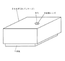
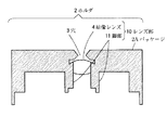
図1は、本発明を適用した撮像装置の第1実施例の構成を示す斜視図である。この撮像装置は、基板1にホルダ2が装着(嵌合)されることにより、それらが一体化されて構成されている。基板1には、後述する図3を参照して説明するように、少なくとも、ホルダ2に設けられた結像レンズ4により結像された光を光電変換し、画像信号を出力する光電変換素子としての、例えばCCDベアチップ12が装着されている。また、ホルダ2には、光を結像させる1つの結像レンズ4が設けられており、その外装は、結像レンズ4に周辺光線が入射しないように、そのような周辺光線を遮断する絞り効果を有し、さらに外光を遮断するパッケージ2Aとされている。なお、パッケージ2Aには、結像レンズ4に、被写体からの光を入射させるための円形状の穴(絞り)3が設けられている。また、この実施例では、穴3は、パッケージ2Aの上部の、ほぼ中央に設けられており、固定アイリスとして機能する。
【0035】
次に、図2は、図1の撮像装置の平面図であり、また、図3は、図2におけるA−A’部分(図2において断面線で示す部分)の断面図である。基板1上には、上述したように、CCDベアチップ12が装着されている他、そのCCDベアチップ12をドライブするドライバ13、CCDベアチップ12の出力をA/D変換するA/D変換器14、その他必要なチップが装着されている(詳細は、図18を参照して後述する)。なお、CCDベアチップ12は、基板1にホルダ2が装着されたときに、ホルダ2に設けられた穴3と対向するような位置に装着されている。但し、基板1の設計上、CCDベアチップ12の装着位置が制限される場合には、先に、CCDベアチップ12の装着位置を決定し、その後、CCDベアチップ12と対向する位置に、穴3を設けるようにすることができる。
【0036】
さらに、基板1の側面には、外部へ信号を出力し、また外部から信号を入力するため(例えば、CCDベアチップ12より出力され、所定の処理が施された画像信号を取り出したり、あるいは基板1に装着された各チップに電源を供給したりするためなど)のリード5が設けられている。なお、図1においては、リード5の図示を省略してある。
【0037】
基板1に装着された各チップは、必要に応じて、接続線によって接続されている。なお、図3では、ドライバ13から引き出されている接続線13Aのみを図示してあり、その他のチップから引き出されている接続線は、図が煩雑になるため省略してある。
【0038】
図4は、CCDベアチップ12の構成例を表している。この実施例においては、CCDベアチップ12は、入力された光に対応する電気信号を出力するCCD素子(電荷結合素子)12Aと、CCD素子12A上に形成され、R,G,B(補色の場合もある)などの所定の波長の光を通過させるカラーフィルタ12Bとで構成されている。但し、カラーフィルタ12Bは、省略される場合もある。
【0039】
この図4に示されているCCDベアチップ12と、図56に示したCCD撮像素子403とを比較して明らかなように、図4に示したCCDベアチップ12には、図56に示したセラミックやプラスチックよりなるパッケージ403Bが省略された構成となされている。従って、その大きさは、図56に示すCCD撮像素子403に較べてより小さいものとすることができる。
【0040】
結像レンズ4は、脚部11とともにレンズ部10を構成している。ここで、図5は、レンズ部10の詳細構成を表した斜視図である。レンズ部10は、透明な材料としての、例えば透明なプラスチック(例えば、PMMAなど)でなり、平行平板に4つの脚が設けられたような、いわばテーブル形状をしている。すなわち、平行平板の中心部分には、単玉レンズとしての結像レンズ4が形成され、さらに、その平行平板の4隅には、結像レンズ4の光軸と平行な方向に延びた、例えば水平断面の形状が長方形である角柱形状の4つの脚部11が設けられている。そして、この4つの脚部11のそれぞれの下部であって、結像レンズ4の光軸と対向する角の部分は、角柱状にくり貫かれ、これにより切欠き11Aが形成されている。なお、4つの脚部11のそれぞれは、その4つの側面のうちの2つ(その2つの側面で構成される角の部分)が、結像レンズ4の光軸と対向するように設けられている。
【0041】
CCDベアチップ12は、その上面(撮像面)から見た形状が、例えば長方形状のチップであり、4つの切欠き11Aのそれぞれは、CCDベアチップ12の4角に精度良く嵌合するようになされている。
【0042】
なお、レンズ部10は、プラスチックを、例えばモールド成形することで構成されており(従って、結像レンズ4はプラスチックモールド単玉レンズである)、これにより結像レンズ4の主点に対する、レンズ部10の各部の寸法の相対的な精度は、充分に高くされている。
【0043】
図2および図3に示すように、以上のように構成されるレンズ部10は、ホルダ2の外装を構成する、蓋形状のパッケージ2Aの内側であって、穴3と対応する位置に、結像レンズ4の光軸が穴3の中心を通るように嵌合されている。そして、レンズ部10の4つの脚部11は、その切欠き11Aのそれぞれが、CCDベアチップ12の4角の部分に嵌合されることにより、CCDベアチップ12に直接接触している。
【0044】
ホルダ2の外装を構成するパッケージ2Aは、遮光性の材料としての、例えばポリカーボネイト樹脂などでなり、同じく遮光性の充填剤(接着剤)20によって基板1と接着されており、これにより、基板1とホルダ2とが一体化されている。
【0045】
図6は、脚部11とCCDベアチップ12とが接触している部分の断面を拡大した拡大図(図3において点線で囲んである部分Zの拡大図)である。同図に示すように、脚部11の下端が、基板1から若干浮いた状態で、切欠き11Aの底面と側面が、CCDベアチップ12の受光面(図中、S1で示す部分)とその側面(図中、S2で示す部分)に、ある程度の圧力をもって、直接接触している(従って、脚部11は、CCDベアチップ12に、いわば突き当てられた状態とされる)。なお、この圧力は、ホルダ2を基板1に嵌合した後、所定の圧力をかけながら、充填剤20を充填することにより基板1とホルダ2とを接着、封止することで生じるようになされている。
【0046】
ホルダ2の、基板1と嵌合させる部分の寸法は、基板1の外形より幾分大きめとされており、従って、基板1とホルダ2とは、脚部11をCCDベアチップ12に接触させる精度を優先する形で接着されている。
【0047】
以上のように、少なくともCCDベアチップ12が装着された基板1と、結像レンズ4が設けられた、絞り効果を有する外装(パッケージ2A)のホルダ2とが一体にされているので、撮像装置を、例えばテレビ会議システムなどに適用する場合などの応用時に、結像レンズ4とCCDベアチップ12との間などの光学的調整が不要であり、従って、その組み込みおよび取扱いが容易になる。その結果、このような撮像装置を用いた装置の製造コストを低減することが可能となる。
【0048】
さらに、上述したように、レンズ部10の各部の寸法の、結像レンズ4の主点に対する相対的な精度は充分に高くされているとともに、その脚部11(切欠き11A)は、CCDベアチップ12の受光面に直接突き当てられているので、結像レンズ4は、その主点が、CCDベアチップ12の受光面と所定の位置関係を満たすように、特別の調整をすることなしに、精度良く配置される。すなわち、結像レンズ4を、低コストで、かつ精度良くマウントすることができる。さらに、この場合、結像レンズ4を精度良くマウントするための調整機構が不要であるから、撮像装置の小型化、軽量化を図ることができる。
【0049】
なお、CCDベアチップ12の撮像面を押圧する脚部11の切欠き11A面に、突起11Aaを生成し、この突起11AaによりCCDベアチップ12を押圧するようにすることもできる。この突起11Aaを半球状または円筒状とすることにより、CCDベアチップ12と脚部11との間の接触が、理論的には点または線で行われるようになるため、CCDベアチップ12や脚部11の面の精度に拘らず、確実にCCDベアチップ12を押圧することが可能となる。
【0050】
あるいはまた、図8に示すように、脚部11の切欠き11Aにテーパ面11Abを形成し、このテーパ面11Abで、CCDベアチップ12の上端部のエッジを押圧するようにしてもよい。このようにすると、CCDベアチップ12の形状のばらつきに拘らず、CCDベアチップ12を確実に押圧することが可能となる。
【0051】
次に、図9および図10を参照して、結像レンズ4の光学特性と脚部11の寸法(長さ)について説明する。図9(A)に示すように、結像レンズ4の合焦位置(結像面)f1は、破線で示すように湾曲する。そして、CCDベアチップ12の受光面(撮像面)は、結像面f1と、結像レンズ4の光軸上において接する理想的像面(湾曲しない平坦な面)f2上の位置に配置される(そのような配置関係になるように、脚部11の長さが設定されている)。
【0052】
しかしながら、そのままだと、撮像面の中央付近(結像面f1と理想的像面f2が接する点の近傍)においては合焦するが、撮像面の中央から離れるほど(図9において、結像面f1と理想的像面f2が接する点から上下方向に離れるほど)、結像面f1の合焦位置撮像面(理想的像面f2)からのデフォーカス量が大きくなる。すなわち、撮像面上の中央部の画像は、フォーカスの合った明瞭な画像となるが、それに較べて周辺部の画像は、所謂ピンボケの画像となる。
【0053】
そこで、撮像面の全体において、均一なデフォーカス量が得られるように、結像レンズ4の光軸上において、球面収差が生じるように、結像レンズ4が設計される。これにより、図9(A)に示すように、本来(球面収差が発生していなければ)、結像面f1と理想的像面f2の接点近傍において集束すべき光が、その位置より、例えば、より遠い位置で集束するようになる。その結果、撮像面の中央部においても、所謂若干ピンボケの状態となり、結局、撮像面全体において、ほぼ均一なフォーカス状態の画像が得られることになる。
【0054】
すなわち、これにより、点光源に対する結像レンズ4の応答の半値幅が、図9(B)および図9(D)に示すように、CCDベアチップ12の受光面上の中央部(図9(B))においても、また、周辺部(図9(D))においても一定で、かつ、CCDベアチップ12の画素ピッチより大きくなるようになされている。
【0055】
ここで、図9(A)または図9(C)は、CCDベアチップ12の中央部または周辺部に平行光線が収束している状態をそれぞれ表しており、図9(B)または図9(D)は、図9(A)または図9(C)に示した場合のCCDベアチップ12の受光面上における光の強度(無限遠にある点光源に対する応答)を表している。本実施例では、CCDベアチップ12の中央部または周辺部それぞれにおける点光源応答の半値幅w1またはw2は、いずれもCCDベアチップ12の画素ピッチのほぼ2倍(好ましくは、例えば1.8倍乃至3倍程度)とされている(CCDベアチップ12の受光面のその他の位置についても同様)。これにより、CCDベアチップ12としては、水平方向が360画素、垂直方向が480画素の、約17万画素の低画素数の素子を用いることができる。
【0056】
このように、点光源応答の半値幅をCCDベアチップ12の画素ピッチの2倍とすることにより、結像レンズ4の空間周波数応答特性は、図10に示すように、CCDベアチップ12のナイキスト限界の空間周波数fn以上の入射成分を充分 に抑圧する特性となる。従って、従来は、図52で説明したように、折り返し歪を低減するための光学LPF112が必要であったが、図1の撮像装置では、そのような光学素子を設けることなく、折り返し歪を低減することができる。その結果、装置の小型化、軽量化、低コスト化を図ることができる。
【0057】
なお、図9においては、光軸近傍の光を、結像レンズ4の結像面f1(理想的像面f2)から所定の距離だけ、結像レンズ4から離れる方向に合焦させるようにしたが、これとは逆に、結像レンズ4に近づく方向に合焦させるようにすることも可能である。
【0058】
また、本実施例では、結像レンズ4は、焦点距離の短いもの(例えば、4mm程度)とされ、さらに絞りとして機能する穴3が小さいもの(例えばその直径は、1.2mm程度のもの)とされている。これにより、被写界深度が深くなり、被写体までの距離が変化しても、ボケの度合いが小さくなる。また、この撮像装置には、例えばいわゆるオートフォーカス機構などのフォーカス機構を設けずに済むようになり、この点でも、装置の小型化、軽量化、低コスト化が図られている。なお、撮像装置を望遠用とする場合には、結像レンズ4としては、焦点距離の長いものを用いるようにし、また、穴3はさらに小さいものとするようにすれば良い。
【0059】
以上の結像面と撮像面の関係をまとめると、図11に示すようになる。すなわち、結像レンズ4の結像面f1は、理想的像面f2に対して湾曲するが、上記実施例においては、この理想的像面f2上に、CCDベアチップ12の撮像面203を配置したことになる。
【0060】
しかしながら、このようにすると、撮像面203の中央部に較べて、周辺部のデフォーカス量が大きくなるため、上述したように、中央部において、球面収差を発生させることで、撮像面203上の全体の画像を均一なフォーカスの画像となるようにしている。
【0061】
しかしながら、この実施例の場合、中央部に較べて、周辺部におけるデフォーカス量が大きくなりすぎる傾向がある。
【0062】
そこで、例えば、図12に示すように、結像レンズ4の結像面f1のほぼ中央(図12の水平方向の中央)にCCDベアチップ12の撮像面203を配置するようにすることもできる。このようにすれば、周辺部と中央部におけるデフォーカス量が、方向は反対となるが、その絶対値はほぼ同一の値となる。但し、この場合、撮像面203と結像面f1の交差する点Aの近傍におけるフォーカス状態が、他の位置におけるフォーカス状態に較べて良好なものとなる。そこで、この点A近傍において、多くの収差が発生するように、結像レンズ4を設計するようにすることができる。このようにすれば、撮像面203の全体において、ほぼ均一なフォーカス状態の画像を得ることができる。
【0063】
次に、図12に示す例に従って、撮像面203の全体において、均一な画像を得るための条件についてさらに詳細に説明する。
【0064】
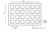
いま、図13に示すように、CCDベアチップ12の有効画素領域の水平方向の長さ(長辺の長さ)Lhを2.0mmとし、垂直方向の長さ(短辺の長さ)Lvを1.5mmとすると、その対角長Ldの長さは、約2.5mmとなる。
【0065】
結像レンズ4の焦点距離fを4.0mmとすると、長辺方向の画角は、次式より約28度と求められる。
長辺方向の画角=2×atan(2.0/(2×4.0))
【0066】
なお、ここで、atanは、逆正接関数を意味する。
【0067】
また、結像レンズ4の焦点距離fと、瞳径Dで規定されるFナンバー(=f/D)を2.8とする。
【0068】
湾曲した結像面f1の半径Rは、ペッツバール和Pの逆数に等しい。すなわち、ペッツバール和Pは、次式で表される。なお、ここで、nは、結像レンズ4の屈折率を表す。
P=Σ1/(nf)
【0069】
いまの場合、結像レンズ4は1個だけであるので、実施の像面201の半径Rは、屈折率nを1.5とすると、次式より求められる。
R=1/P=n×f=1.5×4.0=6.0
【0070】
いま、図13に示すように、有効画素領域の中心から、対角長Ldの1/2の70%までの範囲を均一にすることを考える。この中心から対角長Ldの1/2の70%の位置Lmは、次式から求めることができる。
Lm=0.7×Ld/2=0.4375×Lh=0.875mm
【0071】
図14に示すように、結像面f1の中心をO、結像レンズ4の光軸と理想的像面f2との交点をS、点Sから距離Lmだけ離間した理想的像面f2上の点をQ、結像面f1と、理想的像面f2から結像レンズ4側に距離Zmだけ離れた位置の線205との交点をT、線205と光軸との交点をUとするとき、点T,O,Uで構成される角度θは、ほぼatan(Lm/R)で近似される。従って、点OとUの距離は、結像面f1の半径をR(点OとTの距離=点OとSの距離)とするとき、次式で求められる。
R×cos{atan(Lm/R)}
【0072】
従って、理想的像面f2上の光軸上の点Sからの距離がLmである(像高がLmである)点Qの位置における結像面f1の理想的像面f2からの湾曲量Zmは、R=0.6mm,Lm=0.875mmとして、次式より求めることができる。
Zm=R×(1−cos{atan(Lm/R)})=0.0628mm
【0073】
いま、撮像面203を、理想的像面f2から結像レンズ4側にZm/2の位置に配置するものとすれば、画面の終端部近傍(像高Lmの位置)と画面の中央部において、それぞれZm/2の焦点ズレが発生する。この焦点ズレにより発生する錯乱円の直径αは、
F=f/D=(Zm/2)/α
の関係から、次式より求めることができる。
α=(Zm/2)/F=0.0314/Fmm
【0074】
さらに、円開口によるMTFは、次式より求めることができる。
M(ω)=[J1{πα(k/Lh)}]/{πα(k/Lh)}
【0075】
ここで、J1は、一次の第1種ベッセル関数を表し、k/Lhは、水平方向の空間周波数を表す。従って、kは、水平方向の長さLhを分割する数に対応する。なお、垂直方向の解像特性は、テレビジョンシステムの走査線で決定されるので、ここでは、水平方向だけについて考察する。
【0076】
一次の第1種ベッセル関数J1が最初に0になるときの値は3.83であるから、次式が成立する。
πα(k/Lh)=3.83
【0077】
従って、上記式から、図10に示すMTFのトラップポイントfn(=k/Lh)を求めると、次のようになる。
(k/Lh)=3.83/(πα)=38.8F
【0078】
従って、kは、次のように求めることができる。
k=38.8×F×Lh=38.8×2×F=77.6F
【0079】
従って、上記空間周波数を確保するのに、必要な最低画素数Gは、サンプリング定理に従って、次式より求めることができる。
G=2k=2×77.6F=155F
【0080】
なお、上記演算は、結像レンズ4の屈折率nを1.5として求めたものであるが、もっと高い値(例えば、1.9)とすれば、次式が得られる。
G=2k=200F
【0081】
すなわち、CCDベアチップ12の有効画素ピッチが、有効領域の長辺の1/(200F)より大きいことが、均一な画像を得るための条件となる。このことは、換言すれば、水平方向の有効画素数が200Fより小さいことを意味する。
【0082】
なお、図14において、錯乱円の径αは、結像レンズ4の開口の端部と点Tを結ぶ線が、撮像面203と交差する点の距離として求めることができる。
【0083】
従って、図15に模式的に示すように、図3に示すCCDベアチップ12の撮像面の画素211のピッチPPは、上記条件を満足するように形成される。
【0084】
次に、1つの結像レンズ4を用いて、最も近い距離Sから無限大(∞)までの距離の被写体を、できるだけピンボケが少なくなるようにして撮像するための焦点距離fの条件について説明する。いま、図16に示すように、無限遠の被写体の結像レンズ4による結像位置と、至近の距離Sの被写体の結像レンズ4による結像位置とのずれ量をgとすると、結像の公式より次式が成立する。
g×(S−f)=f2
【0085】
距離Sは、焦点距離fより十分大きいことを利用して上式を整理すると、次式が得られる。
g=f2/(S−f)=f2/S
【0086】
このズレ量gの範囲において、全体的に焦点のずれ量を少なくするには、CCDベアチップ12の撮像面203を、ずれ量gの中間点(g/2の位置)に設定するようにすればよい。
【0087】
図13における場合と同様に、撮像素子の画面の長辺をLh、像面湾曲の半径をR(=n×f)とするとき、像高Lにおける像面の湾曲量Zは、次式より求めることができる。
Z=R×(1−R2−L2)1/2
ここで、L2/R2は、1より十分小さいので、上記式は次のように整理することができる。
Z=R×(1−(1−L2/(2×R2)))
=L2/(2×R)=L2/(2×n×f)
【0088】
総合的なピントずれ量Dの自乗は、g/2とZの間に相関関係が存在しないため、次式に示すように、それらの自乗和として表すことができる。
D2=(g/2)2+Z2
=(f2/2×S)2+(L2/(2×n×f))2
=(f4/4×S2)+L4/(4×n2×f2)
【0089】
上記式で得られるD2の極小値を与えるfを求めるために、上記D2をfで微分した式を0とおくと、次式が得られる。
f3/S2−L4/(2×n2×f3)=0
【0090】
この式を解いて、次式が得られる。
f=((S2×L4)/(2×n2))(1/6)
【0091】
すなわち、上記式で与えられる焦点距離fを結像レンズ4で得るようにすればよいのであるが、厳密に上記式で与えられる値に設定しなくとも、ある幅を持たせることが可能である。
【0092】
すなわち、一般的に、画像で重要なのは、画面の中心から画面の対角長の1/2の7割までであるから、この範囲を均一にピンボケが生じないようにするには、像高Lを対角長の1/2の長さの0.35倍乃至0.5倍の長さに設定すればよい。画面のアスペクト比を4:3とすると、対角長の1/2の長さは、(5/8)×Lhとなるので、像高Lは、次の範囲に設定すればよいことになる。
0.35×(5/8)×Lh
=0.219Lh<L<0.5×(5/8)×Lh
=0.312Lh
【0093】
また、テレビ会議などへの応用を考慮すると、上記した至近距離Sは、200mm乃至300mmであればよい。さらに、結像レンズ4の屈折率nは、
n=1.4乃至1.9
である。これらの条件を上記焦点距離fの式に代入して整理すると、次式が得られる。
1.53×(Lh(2/3))<f<2.46×Lh(2/3)
【0094】
すなわち、上記式で規定される範囲に1枚の結像レンズ4の焦点距離fを設定すれば、至近距離Sから無限遠に存在する被写体をピンボケさせずに撮像することができる。
【0095】
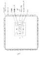
図17は、焦点距離f(横軸)と総合的なピントずれ量Dの自乗の平方根((D2)1/2)(縦軸)の計算例を表している。この場合においては、L=0.63mm,S=200mm,n=1.5とされている。
【0096】
すなわち、この例においては、焦点距離fを約4mmに設定すると、ピントずれ量が最も少ないことがわかる。
【0097】
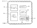
次に、図18および図19を参照して、図1と図3に示す撮像装置の製造方法について説明する。まず、図18に示すように、基板1上にCCDベアチップ12、さらには必要に応じてその他のチップを装着し、必要に応じて電気的に接続する。本実施例では、その他のチップとして、ドライバ13,A/D変換器14、タイミングジェネレータ15、メモリ(2ポートメモリ)16、および信号処理回路17が装着されている。さらに、基板1に、必要なリード5を設け、必要に応じて、基板1上に装着されたチップとの電気的な接続を行う。
【0098】
一方、図19に示すように、遮光性の材料または透明の材料を用い、穴3を設けたパッケージ2Aまたはレンズ部10をそれぞれモールド成形して、パッケージ2Aの穴3の部分に、レンズ部10を嵌合することで一体化し、ホルダ2を製造する。
【0099】
そして、基板1とホルダ2とを、レンズ部10の脚部11を、CCDベアチップ12に突き当てた状態で、図3に示したように充填剤20を充填することで一体化する。
【0100】
上述したように、基板1とホルダ2とを一体化する際には、特別の調整をする必要がないので、容易かつ低コストで、撮像装置を製造することができる。
【0101】
なお、上述の場合には、パッケージ2Aまたはレンズ部10を、それぞれ別にモールド成形した後、これらを一体化することでホルダ2を製造するようにしたが、この他、例えば図20に示すように、ホルダ2は、遮光性の材料および透明の材料を用いて、パッケージ2Aおよびレンズ部10を同時にモールド成形することによって製造するようにすることも可能である。さらに、この場合、図21に示すように、レンズ部10の脚部11は、透明の材料ではなく、遮光性の材料を用いて構成するようにすることができる。この場合、脚部11における光の反射を防止することができ、その結果、フレアを低減することが可能となる。
【0102】
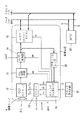
図22は、図1の撮像装置を適用したビデオカメラの電気的構成例を表している。被写体からの光は、穴3を介して結像レンズ4に入射し、結像レンズ4は、その光を、CCDベアチップ12の受光面に結像させるようになされている。CCDベアチップ12は、ドライバ13から供給される各種のタイミング信号yv,yh,ysにしたがって動作するようになされており、結像レンズ4により結像された光を光電変換し、その結果得られる画像信号を、cds処理回路(相関2重サンプリング処理回路)21に出力するようになされている。ドライバ13は、タイミングジェネレータ15より供給される、CCDベアチップ12をドライブするためのタイミング信xv,xh,xsを、そのレベルを変換するとともに、インピーダンスの変換を行うことで、タイミング信号yv,yh,ysとする。そして、これをCCDベアチップ12に与えることで、CCDベアチップ12をドライブするようになされている。
【0103】
A/D変換器14は、タイミングジェネレータ15から供給されるサンプリングクロックpaにしたがって、cds処理回路21からの画像信号をサンプリングし、これにより画像信号をディジタルの画像データとして、メモリ16およびアキュームレータ22に出力するようになされている。なお、A/D変換器14は、外部から供給されるリファレンス電圧vrefを基準に、サンプル値に割り当てるビットを決定するようになされている。タイミングジェネレータ15は、外部のクロック発生回路31から供給されるクロックに基づいて、各種のタイミング信号を生成するようになされている。すなわち、タイミングジェネレータ15は、CCDベアチップ12で発生された電荷を垂直または水平方向にそれぞれ転送するためのタイミング信号xvまたはxh、CCDベアチップ12で発生された電荷をディスチャージする(CCDベアチップ12のサブストレートに排出する)ためタイミング信号(いわゆるシャッタパルス)xs、cds処理回路21を動作させるためのタイミング信号sh、A/D変換器14でのサンプリングのタイミングを与えるためのサンプリングクロックpa、およびメモリ16での画像データの書き込みのタイミングを与えるためのタイミング信号wを生成するようになされている。
【0104】
メモリ16は、例えば、データの読み出しと書き込みとが同時に可能な2ポートメモリで、A/D変換器14からの画像データを、タイミングジェネレータ15から供給されるタイミング信号wにしたがって記憶するようになされている。メモリ16に記憶された画像データは、外部のMPU(マイクロプロセッサユニット)32によって読み出されるようになされている。なお、MPU32による、メモリ16からの画像データの読み出しは、MPU32が、アドレスバスadrsを介して、メモリ16に所定のアドレスを与えることにより、そのアドレスに記憶された画像データが、データバスdata上に出力され、これをMPU32が取り込むことによって行われるようになされている。
【0105】
cds処理回路21は、タイミングジェネレータ15から供給されるタイミング信号shにしたがって動作するようになされており、CCDベアチップ12からの画像信号に対し、いわゆる相関2重サンプリング(correlative double sampling)処 理およびその他の必要な処理を施し、これにより画像信号に含まれる雑音成分を低減して(あるいは取り除いて)、A/D変換器14に出力するようになされている。
【0106】
アキュームレータ22は、A/D変換器14から出力される画像データのうち、CCDベアチップ12の受光面の主要部(例えば、中心部分など)に対応するものの積算値を演算し、タイミングジェネレータ15に出力するようになされている。タイミングジェネレータ15は、アキュームレータ22から供給される積算値が所定の規定値から大きくずれないように、CCDベアチップ12で発生された電荷をディスチャージするためのタイミング信号、すなわちシャッタパルスxsのタイミングを制御するようになされており、これにより電子的にアイリスの調整が行われるようになされている。すなわち、積算値が大きくなったら、露光時間(電荷蓄積時間)を短くし、積算値が小さくなったら、露光時間を長くする。なお、アキュームレータ22は、フィールド周期(場合によってはフレーム周期)でリセットされるようになされている。従って、アキュームレータ22からは、1フィールド(または1フレーム)ごとの画像データの積算値が出力される。
【0107】
クロック発生回路31は、リード5を介して、タイミングジェネレータ15と接続されており、ビデオカメラを動作させるためのクロックを発生し、タイミングジェネレータ15に供給するようになされている。MPU32は、アドレスバスadrsまたはデータバスdataとリード5とを介して、撮像装置(メモリ16)から画像データを読み出し、所定の信号処理を施すようになされている。
【0108】
また、外部からは、リード5を介して、各チップの電源となる電圧Vd、グランドとしての所定の基準電圧gnd、およびCCDベアチップ12をドライブするための電圧Vhが供給されるようになされている。
【0109】
なお、cds処理回路21およびアキュームレータ22は、図18の信号処理回路17に相当する。
【0110】
次に、その動作について説明する。被写体からの光は、固定絞りとして機能する穴3を介して、結像レンズ4に入射し、この光は、結像レンズ4によってCCDベアチップ12の受光面上に結像される。
【0111】
ここで、図23は、結像レンズ4から出射された、撮像対象外の光Lが、脚部11の手前側の面で反射された状態を示している。上述したように、脚部11は、その2つの側面が、結像レンズ4の光軸と対向しており、さらに、その断面は長方形であるから、その2つの面で構成される角の部分の角度aは、直角である。従って、同図に示すように、撮像対象外の光Lが、脚部11の側面で反射された場合には、その反射光は、CCDベアチップ12の受光面に到達することはない。よって、脚部11が設けられていることによるフレアの増加は、ほとんどない。
【0112】
なお、角度aは、直角の他、鋭角であっても良い。ただし、角度aを鈍角にすると、図23において、脚部11の手前側の面で反射された光が、次第にCCDベアチップ12側に入射するようになるので好ましくない。
【0113】
また、脚部11には、例えば遮光性の塗料を塗布するなどして、そこに入射した光をCCDベアチップ12に到達させないようにすることも可能である。さらに、脚部11の断面の形状は、長方形以外の四角形、あるいは三角形、五角形などにすることも可能である。但し、フレアの増加の防止のためには、脚部11の側面のうち、少なくとも1つの隣接する側面が構成する角の部分の角度は直角または鋭角とし、その角の部分が、結像レンズ4の光軸と対向するようにする必要がある。
【0114】
図22に戻り、CCDベアチップ12では、そこで受光された光が光電変換され、その光に対応する画像信号が、ドライバ13からのタイミング信号にしたがって、cds処理回路21に出力される。cds処理回路21では、CCDベアチップ12からの画像信号に対し、相関2重サンプリング処理が施され、A/D変換器14に出力される。A/D変換器14では、cds処理回路21からの画像信号がサンプリングされ、これによりディジタルの画像データとされて、アキュームレータ22に供給される。アキュームレータ22では、A/D変換器14からの画像データのうち、上述したような所定のものが積算され、その積算値がタイミングジェネレータ15に出力される。タイミングジェネレータ15は、クロック発生回路31からのクロックに基づいて、各種のタイミング信号を生成しており、アキュームレータ22から積算値が供給されると、その積算値が所定の規定値から大きくはずれないように、シャッタパルスxsの発生タイミングを変化させる。
【0115】
また、A/D変換器14から出力された画像データは、アキュームレータ22の他、メモリ16にも供給されて記憶される。MPU32では、必要なときに、メモリ16から画像データが読み出され、所定の処理が施される。
【0116】
撮像装置としての1つのパッケージには、光電変換を行い、画像信号を出力するCCDベアチップ12、CCDベアチップ12の出力をA/D変換するA/D変換器14、A/D変換器14の出力を記憶するメモリ16が設けられているため、MPU32から撮像装置を見た場合、撮像装置はメモリと等価であり、従って、撮像装置とその外部のブロックとの同期関係を意識する必要がない。その結果、撮像装置を、上述したようなビデオカメラ、あるいはその他の装置に適用する場合に、その組み込みや取扱いを容易に行うことができる。
【0117】
この他、メモリ16に代えて、NTSCエンコーダ等のカメラ回路を配置し、画像データをNTSC方式のビデオ信号に変換して出力するようにしてもよい。
【0118】
なお、本実施例においては、結像レンズ4からの光を光電変換する光電変換素子として、CCDのベアチップを用いるようにしたが、光電変換素子としては、その他、例えばCMOS型撮像素子などのコンデンサにチャージされた電荷を画像信号として読み出す破壊読み出し型撮像素子のベアチップを用いることも可能である。さらに、光電変換素子としては、破壊読み出し型撮像素子以外のものを用いることも可能である。CCD以外の光電変換素子を用いる場合には、cds処理回路21は設けずに済むようになる。
【0119】
また、本実施例では、メモリ16を2ポートメモリとしたが、メモリ16としては、そのような2ポートメモリでない、通常のメモリを用いることも可能である。但し、メモリ16が2ポートメモリでない場合、CPU32よる画像データの読み出しと、A/D変換器14による画像データの書き込みとの調整を図るための回路が必要となる。
【0120】
さらに、本実施例においては、レンズ部10の4つの脚部11のそれぞれを、CCDベアチップ12の4角に直接接触させるようにしたが、この4つの脚部11は、例えばCCDベアチップ12の4辺(図2において、▲印を付してある部分)のそれぞれに接触させるように設けることなどが可能である。但し、この場合、脚部11で反射された反射光がCCDベアチップ12に入射することによりフレアを生じ、またCCDベアチップ12からの接続線が引き出しにくくなるので、脚部11は、本実施例で説明したように、CCDベアチップ12の4角に接触させるように設けるのが好ましい。
【0121】
あるいはまた、図24に示すように、レンズ部10の脚部11を2つとし、図2において、▲印を付して示した辺のうち、対向する2つの辺を切欠き11Aで保持するようにすることも可能である。さらに、この場合においても、図7または図8に示した突起11Aaまたはテーパ面11Abを設けることもできる。
【0122】
また、図3の実施例においては、レンズ部10をパッケージ2A(ホルダ2)と一体化するようにしたが、図25に示すように、両者の間に間隙を設けるようにすることも可能である。この場合、脚部11の下端は充填剤20で基板1に装着される。このようにすれば、ホルダ2に対して、外から圧力が加わったような場合に、それがレンズ部10に直接伝達されることが少なくなり、レンズ部10の破損を抑制することが可能となる。この実施例の場合、穴3による絞りの位置が結像レンズ4と離れるが、絞りの効果はそれ程敏感ではないので、実用上、殆ど問題はない。
【0123】
ところで、一般的に、合成樹脂は、ガラスに比べて、熱膨張率が約10倍大きく、かつ、屈折率の温度変化がガラスの約100倍大きい。その結果、結像レンズ4を合成樹脂で形成すると、温度が変化したとき、焦点距離が変化してしまい、調整機構を設けずに、広い温度変化にわたって使用できるようにすることが困難になる。そこで、本実施例においては、例えば次のようにして、この調整機構を実質的に設けるようにしている。
【0124】
すなわち、図26に示すように、温度が上昇すると、脚部11の長さL11が長くなる。また、凸レンズの屈折率nと焦点距離fとの間には、ほぼ以下の式が成立する。
f=K/(2(n−1))
なお、ここで、Kは、レンズ球面の曲率に関係する係数である。
【0125】
従って、温度が高くなると、図26に示す結像レンズ4の焦点距離fが変化する。
【0126】
いま、単位温度変化に対する屈折率変化をa(/度)、脚部11の線膨張係数をb(/度)とする。通常、樹脂レンズのaは負の値であり、そのオーダは10-5乃至10-4であり、bは正の値であり、そのオーダは10-5乃至10-4である。
【0127】
いま、常温において、温度がT(度)だけ上昇したときの焦点位置変化をΔfとすると、焦点位置変化Δfは、次のように表すことができる。
Δf=K/(2(n−1+a×T))−R/(2(n−1))
=−a×T×K/(2(n−1+a×T)×(n−1))
=−a×T×f/(n−1+a×T)
【0128】
但し、
R=2×(n−1)×f
である。
【0129】
通常、n−1≫a×Tが成立するから、上記式は次のように表すことができる。
Δf=−a×T×f/(n−1)
【0130】
また、温度がTだけ上昇したとき、脚部11の長さL11の増加量ΔLは、次式で表すことができる。
ΔL=b×T×L11
【0131】
従って、実際の焦点距離面の移動量Δhは、次のようになる。
Δh=Δf−ΔL
【0132】
そこで、Δhが結像レンズ4の焦点深度ΔZに収まるように設計を行うことにより、すなわち、次式
|−a×f/(n−1)−b×L11|<(ΔZ/T)
を満足するように設計を行うことにより、温度が変化したとしても、合焦位置f1をCCDベアチップ12の受光面上に位置させることが可能となる。
【0133】
また、上記実施例では、レンズの収差などを利用して入射光像の空間周波数を制限し、CCDベアチップ12上で発生する折り返し歪みを低減させるようにしている。しかしながら、カメラの用途によっては、単板カラーカメラで発生する色モアレを充分に抑圧することが要求される。この場合、特定の空間周波数のみを鋭く抑圧する必要があるが、上記した実施例のような空間周波数制限法では、特定の空間周波数のみを鋭く抑圧することは困難である。
【0134】
そこで、例えば図27に示すように、結像レンズ4をその中心を通る水平面で2分割して、結像レンズ4Aと4Bとし、その分割面上で、結像レンズ4Aを結像レンズ4Bに対して水平方向に角度θだけ回動して、不連続面4Cを形成した構成のレンズを用いることができる。この結像レンズ4を上面からみると、図28に示すようになる。
【0135】
この場合、被写体からの光が上方の結像レンズ4Aを透過した後、CCDベアチップ12に結像する位置と、下方の結像レンズ4Bを透過してCCDベアチップ12上に結像する位置とは、距離Qだけ水平方向に離れている。すなわち、このとき、次式が成立する。
θ=2×atan(Q/2f)
【0136】
その結果、この結像レンズ4A,4BによるMTFは、図29に示すようになり、空間周波数が1/(2Q)において、鋭く低下する特性となる。
【0137】
なお、このような特性を得るには、結像レンズ4の不連続面の方向を必ずしも水平方向にする必要はなく、図30に示すように、垂直方向(図30(A))あるいは斜め方向(図30(B))にしてもよい。
【0138】
さらに、上記実施例においては、レンズ部10の脚部11をCCDベアチップ12上に直接当接するようにしたが、基板1上に当接させるようにすることも可能である。図31は、この場合の例を表している。
【0139】
すなわち、図31の実施例においては、基板1にCCDベアチップ12より若干大きい形状の凹部1Aが形成されている。そして、CCDベアチップ12は、充填剤20により、この凹部1Aに接着されており、レンズ部10の脚部11は、その切欠き11Aが基板1の凹部1Aの角部に係止されている。そして、脚部11の外周は、充填剤20により基板1に接着されている。その他の構成は、図3における場合と同様である。
【0140】
図32は、図31の実施例における、CCDベアチップ12とレンズ部10を基板1に取り付けるための工程を表している。
【0141】
すなわち、最初に、図32(A)に示すように、吸着型のICチップをつかむための治具501により、CCDベアチップ12の撮像面を吸着する。そして、図32(B)に示すように、基板1の凹部1Aに予め充填剤20を塗布しておき、図32(C)に示すように、治具501に保持されているCCDベアチップ12を基板1の凹部1A内にダイボンディングする。このとき、基板1の上面1Bと治具501の面501Aが当接し、CCDベアチップ12の撮像面は、基板1の上面1Bと同一の高さに位置決めされる。
【0142】
次に、図32(D)に示すように、レンズ部10の切欠き11Aを、基板1の凹部1Aを形成することにより形成される角部に係合する。そして、さらに図32(E)に示すように、脚部11の外周と基板1の上面との間に、充填剤20を充填して、接着する。
【0143】
なお、この実施例の場合、CCDベアチップ12を凹部1A内にダイボンディングしているので、CCDベアチップ12の撮像面の高さを正確に位置決めすることが可能であるが、水平面内(XY平面内)における取り付け精度は若干低下する。しかしながら、CCDベアチップ12の撮像面から離れた位置にレンズ部10の脚部11を配置することができるため、CCDベアチップ12のボンディングワイヤ(図示せず)があったとしても、これを容易に回避して、レンズ部10を取り付けることができる。また、脚部11における不良反射による影響を軽減することができる。
【0144】
さらに、例えば、レンズ部10の脚部11を、図33に示すような、四方の面が囲まれている箱型形状の脚部とし、ゴミなどが内部に進入するのを防止するようにすることができる。また、このとき、図33に示すように、脚部11の底面に突起11Aaを設けることができる。あるいはまた、例えば図34に示すように、対向する2つの脚部を設ける構成としてもよい。そして、この場合において、脚部11の底面に円筒上の突起11Aaを形成することができる。
【0145】
図35は、図22に示した撮像装置の他の構成例を示している。すなわち、この実施例においては、図22におけるクロック発生回路31が、撮像装置の内部に収容されているとともに、メモリ16の代わりにカメラ処理回路511が設けられ、A/D変換器14の出力が供給されている。そして、カメラ処理回路511において、輝度信号と色差信号、あるいは、R,G,B信号などが生成される。さらに、ここにエンコーダを内蔵させ、例えばNTSC方式のフォーマットのビデオデータに変換させるようにしてもよい。その出力は、FIFOメモリ512に供給され、一旦記憶された後、所定のタイミングで読み出される。FIFOメモリ512より読み出されたデータは、パラレルシリアル(P/S)変換器513に入力され、パラレルデータがシリアルデータに変換され、ドライバ515を介して、出力端子517から、正相のデータおよび逆相のデータとして出力される。
【0146】
一方、入力端子518から入力された正相および逆相のデータは、レシーバ516で同相成分が除去された後、調停回路514に入力される。調停回路514は、入力された制御データに対応して、FIFOメモリ512を制御し、カメラ処理回路511からのデータを書き込み、所定のタイミングで読み出す制御を行うとともに、ドライバ515を制御し、パラレルシリアル変換器513からのデータを出力させる。
【0147】
このドライバ515とレシーバ516は、IEEE1394に規定されているシリアルバスの標準規格に準拠するものである。この他、例えば、USDに準拠するようにすることも可能である。
【0148】
このように、シリアルにデータを出力し、また入力を受けるように構成することで、パラレルデータを入出力する場合に較べて、撮像装置が大型化することを防止することができる。
【0149】
なお、A/D変換器14より前段の動作は、図22における場合と同様であるので、その説明は省略する。
【0150】
[第2実施例]
図36は、本発明を適用した撮像装置の第2実施例の構成を示す斜視図である。この撮像装置も、第1実施例の撮像装置と同様に、基板51にホルダ(パッケージ)52が装着(嵌合)されることにより、それらが一体化されて構成されている。但し、この撮像装置は、第1実施例の撮像装置より、さらに小型化、軽量化、低価格化を図るために、ホルダ52には、その一部として、光を結像するための1つの結像レンズ54が上部に形成されており(従って、このホルダ52は、第1実施例におけるレンズ部10に相当する)、また、基板51には、結像レンズ54により結像された光を光電変換し、画像信号を出力するCCDベアチップ12(図37乃至図39)のみが装着されている。なお、ホルダ52は、透明の材料(例えば、透明なプラスチック(例えば、PMMAなど)など)でなり、その、結像レンズ54の部分を除いた外装部分には、CCDベアチップ12に、それほど重要でない周辺光線が入射しないように、そのような周辺光線を遮断する絞り効果を有する遮光性の遮光膜61が形成(コーティング)されている。また、CCDベアチップ12は、第1実施例における場合と同様のものである。
【0151】
図37は、図36の撮像装置の平面図であり、また、図38または図39は、それぞれ図36におけるB−B’部分またはC−C’部分の断面図である。基板51上には、上述したように、CCDベアチップ12のみが装着されている。なお、CCDベアチップ12は、基板51にホルダ52が装着されたときに、ホルダ52の一部として形成されている結像レンズ54と対向するような位置に装着されている。
【0152】
さらに、基板51の側面には、基板1と同様に、外部へ信号を出力し、また外部から信号を入力するためのリード55が設けられている。なお、図36、図38、および図39においては、リード55の図示を省略してある。
【0153】
基板51に装着されたCCDベアチップ12からは、信号の授受のための接続線12Aが引き出されており、各接続線12Aは、所定のリード55と接続されている。
【0154】
ホルダ52は、上述したように、透明な材料でなり、その形状は、その水平方向の断面が長方形である箱型(図38に示す状態において、上下を逆にした場合)とされている。そして、その底面(撮像装置の上部)の中心部分には、単玉レンズとしての結像レンズ54が形成されており、その結像レンズ54の部分を除き、内側も含めて無反射コーティングがなされている。すなわち、ホルダ52には、遮光性の塗料が塗布され、またはこれに準ずる加工がなされており、これにより遮光膜61が形成されている。
【0155】
いま、図37に示すように、CCDベアチップ12の接続線12Aが引き出されている方の辺(図37において垂直方向の辺)の長さは、引き出し線12Aのない方の辺(図37において水平方向の辺)の長さより長い。従って、ホルダ52の4つの側面である、対向する2組の脚部62のうち、図37において水平方向で対向する脚部62どうしの距離は、図38に示すように、短いものとなり、また、図37において垂直方向で対向する脚部62どうしの距離は、図39に示すように、長いものとなる。そして、一方の対向する脚部62は、内側の部分がくり貫かれ、これにより切欠き62Aが形成されている。そして、この切欠き62Aの部分は、CCDベアチップ12の縦の2辺の部分に精度良く嵌合するようになされている。
【0156】
なお、本実施例では、ホルダ52は、例えば透明なプラスチックをモールド成形することで構成されており(従って、結像レンズ54も、結像レンズ4と同様に、プラスチックモールド単玉レンズである)、これにより結像レンズ54の主点に対する、ホルダ52の各部の寸法の相対的な精度は、充分に高くされている。
【0157】
ホルダ52の一方の対向する脚部62は、その切欠き62Aの部分のそれぞれが、CCDベアチップ12の図37における縦の2辺の部分に嵌合されることにより、CCDベアチップ12に直接接触している。この一方の対向する脚部62の長さ(図38における垂直方向の長さ)は、他方の対向する脚部62の長さ(図39における垂直方向の長さ)より幾分短くされている。これにより、一方(図38)の対向する脚部62の下端が、基板51から若干浮いた状態で、切欠き62Aが、CCDベアチップ12の受光面とその側面に、ある程度の圧力をもって、直接接触している(従って、一方(図38)の脚部62は、CCDベアチップ12に突き当てられた状態とされる)。なお、この圧力は、ホルダ52を基板51に嵌合した後、所定の圧力をかけながら、充填剤20を充填することにより基板51とホルダ52とを接着、封止することで生じるようになされている。
【0158】
ホルダ52の、他方(図39)の対向する脚部62は、一方(図38)の対向する脚部62より幾分長めであるが、切欠き62Aが、CCDベアチップ12の受光面に突き当てられたときに、その下部が基板51に接触しない程度の長さとされている。従って、基板51とホルダ52とは、一方(図38)の対向する脚部62をCCDベアチップ12に接触させる精度を優先する形で接着されている。
【0159】
なお、結像レンズ54の光学特性、およびCCDベアチップ12に突き当てられる2つの脚部(一方(図38)の対向する脚部)62の寸法(長さ)は、図11または図12で説明した場合と同様になされている。
【0160】
以上のように、この実施例においても、CCDベアチップ12が装着された基板51と、結像レンズ54および絞り効果を有する遮光膜61が形成されたホルダ52とを一体化するようにしたので、撮像装置の応用時の組み込みおよび取扱いが容易になり、製造コストを低減することが可能となる。
【0161】
さらに、ホルダ52の各部の寸法の、結像レンズ54の主点に対する相対的な精度は充分に高くされているとともに、その一方(図38)の対向する脚部62は、CCDベアチップ12の受光面に直接突き当てられているので、結像レンズ54は、第1実施例の結像レンズ4における場合と同様に、特別の調整をすることなしに、精度良く配置することができ、これにより、撮像装置の小型化、軽量化を図ることができる。
【0162】
また、ホルダ52には、その一部として、結像レンズ54を形成し、基板51には、CCDベアチップ12のみを装着するようにしたので、第1実施例における場合に比較して、撮像装置のさらなる小型化、軽量化、低価格化を図ることができる。
【0163】
さらに、図39に示すように、ホルダ52の、他方の対向する脚部62どうしの距離は、CCDベアチップ12の図37における水平方向の長さよりも長いものとされているので、接続線12Aの引き回しを容易に行うことができる。
【0164】
次に、図36乃至図39に示した撮像装置の製造方法について説明する。まず、基板51上にCCDベアチップ12を装着するとともに、リード55を設け、必要に応じて、CCDベアチップ12の接続線12Aとリード55との接続を行う。一方、透明の材料を用い、結像レンズ54を有し、脚部62に切欠き62Aを設けたホルダ52をモールド成形した後、遮光膜61を形成する。そして、基板51とホルダ52とを、一方の対向する脚部62を、CCDベアチップ12に突き当てた状態で、図38および図39に示したように充填剤20を充填することで一体化する。
【0165】
基板51とホルダ52とを一体化する際には、第1実施例の場合と同様に、特別の調整をする必要がないので、容易かつ低コストで、撮像装置を製造することができる。
【0166】
なお、この場合においても、透明の材料と遮光性の材料を用いて、ホルダ52(結像レンズ54)をモールド成形することができる。これにより、図40に示すように、結像レンズ54を透明材料で形成し、脚部62を遮光性材料で形成することができる。
【0167】
あるいはまた、図41に示すように、透明材料で結像レンズ54を脚部62を含めて成形し、その外周側と内周側に、それぞれ外シート91と内シート92をかぶせるようにして、ホルダ52を形成するようにしてもよい。この外シート91と内シート92は、それぞれ遮光性材料で、結像レンズ54の外周側と内周側の形状に対応して形成されている。あるいは、外シート91と内シート92をかぶせる代わりに、黒く塗装するようにしてもよい。
【0168】
この他、例えば図42に示すように、CCDベアチップ12を基板51上に装着し、さらに結像レンズ54を基板51上に装着した状態で、基板51と結像レンズ54の外周を黒色の樹脂66でモールドするようにすることもできる。
【0169】
また、この撮像装置は、図22に示したドライバ13より出力される信号を、外部から、リード55を介して入力することでドライブし、その結果、やはりリード55を介して得られる画像信号は、外部において、必要に応じて信号処理される。
【0170】
さらに、本実施例においては、結像レンズ54からの光を光電変換する光電変換素子として、CCDベアチップ12を用いるようにしたが、光電変換素子としては、第1実施例で説明したように、例えば破壊読み出し型撮像素子やその他のものを用いることが可能である。
【0171】
なお、図39の実施例における基板51を、図43に示すように大きくし、その基板51上に各種の部品67を配置するようにすることもできる。
【0172】
また、結像レンズとしては、1段の構成だけではなく、図44に示すように、結像レンズ54A(凸レンズ)と結像レンズ54B(凹レンズ)の2段の構成とすることもできる。もちろん、3段以上の構成とすることも可能である。
【0173】
[第3実施例]
図45は、本発明を適用した撮像装置100を組み込んだビデオカメラの構成例を示している。なお、図中、図22における場合と対応する部分については、同一の符号を付してある。撮像装置100は、第1実施例または第2実施例の撮像装置と同様に構成されている。但し、基板1(または51)には、CCDベアチップ12とA/D変換器70が装着されている。なお、本実施例では、撮像装置100は、第1実施例の撮像装置と同様に構成されているものとする。
【0174】
A/D変換器70は、シリアル出力型のA/D変換器で、CCDベアチップ12より出力される画像信号を、その出力周期(ある画素に対応する画像信号が出力されてから、次の画素に対応する画像信号が出力されるまでの時間)の1/2の周期を有するサンプリングクロックp1のタイミングでA/D変換し、その結果得られるディジタルの画像データを、シリアルデータの形で出力するようになされている。
【0175】
なお、A/D変換器70は、外部から供給されるリファレンス電圧vrefを基準に、サンプル値に割り当てるビットを決定するようになされている。
【0176】
また、A/D変換器70としては、サンプリングの結果得られた画像データを、パラレルデータの形で出力するパラレル出力型のA/D変換器を用いることも可能である(この場合、後述するS/P変換器71は不要となる)。但し、A/D変換器70として、パラレル出力型のA/D変換器を用いた場合、パラレルデータの形で出力する画像データのビット数分のリード5を設ける必要があるのに対し、A/D変換器70をシリアル出力型のA/D変換器とした場合には、画像データを出力するために必要なリード5は1つで済む。従って、A/D変換器70としては、シリアル出力型のものを用いた方が、撮像装置100を小型に構成することができる。
【0177】
S/P(シリアル/パラレル)変換器71は、撮像装置100(A/D変換器70)より出力されるシリアルの画像データをパラレルの画像データに変換し、D−FF(遅延型フリップフロップ)72および減算回路73に出力するようになされている。D−FF72は、サンプリングクロックp1と同一の周期を有するクロックp2にしたがって、S/P変換器71からの画像データを1クロック分だけ遅延し、減算回路73に出力するようになされている。減算回路73は、S/P変換器71からの画像データと、D−FF72の出力との差分を演算し、その差分値をD−FF74に出力するようになされている。D−FF74は、クロックp2の2倍の周期(画素の出力周期と同一の周期)を有するクロックp3にしたがい、減算回路73から出力される差分値を、1つおきにラッチして、カメラ信号処理回路75に出力するようになされている。
【0178】
カメラ信号処理回路75は、D−FF74の出力に所定の信号処理を施すようになされている。
【0179】
タイミングジェネレータ76は、図示せぬクロック発生回路から供給されるクロックに基づいて、各種のタイミング信号を生成するようになされている。すなわち、タイミングジェネレータ76は、図22のタイミングジェネレータ15と同様に、CCDベアチップ12をドライブするためのタイミング信号を生成し、ドライバ13に供給する。さらに、タイミングジェネレータ76は、上述したような周期のクロックp1,p2,p3を生成し、A/D変換器70,D−FF72,73にそれぞれ供給する。また、タイミングジェネレータ76は、S/P変換器71が動作するのに必要なクロックを生成し、S/P変換器71に供給する。なお、タイミングジェネレータ76が出力する各種のタイミング信号は、相互に同期のとれたものとされている(クロック発生回路からのクロックに同期したものとされている)。
【0180】
次に、図46のタイミングチャートを参照して、その動作について説明する。被写体からの光は、結像レンズ4に入射し、この光は、結像レンズ4によってCCDベアチップ12の受光面上に結像される。CCDベアチップ12では、そこで受光された光が光電変換され、その光に対応する画像信号outが、ドライバ13からのタイミング信号にしたがって、A/D変換器70に出力される。ここで、図46(A)は、CCDベアチップ12より出力される画像信号outを示している。
【0181】
A/D変換器70では、CCDベアチップ12より出力された画像信号outが、その出力周期の1/2の周期を有するサンプリングクロックp1(図46(B))の、例えば立ち上がりエッジのタイミングでA/D変換され、その結果得られるディジタルの画像データsa(図46(C))が、シリアルデータの形で、S/P変換器71に出力される。S/P変換器71では、A/D変換器70からのシリアルの画像データsaがパラレルの画像データsb(図46(E))に変換され、D−FF72および減算回路73に出力される。
【0182】
なお、S/P変換器71では、変換処理に1クロック分の時間を要し、このため、画像データsb(図46(E))は、画像データsa(図46(C))より1クロックだけ遅れたものとなる。
【0183】
D−FF72では、タイミングジェネレータ76より供給される、サンプリングクロックp1と同一の周期を有するクロックp2(図46(D))の、例えば立ち上がりエッジのタイミングで、S/P変換器71からの画像データsbがラッチされ、これにより1クロック分だけ遅延され、図46(F)に示すような画像データscとされて、減算回路73に出力される。
【0184】
ここで、サンプリングクロックp1と同一の周期を有するクロックp2は、CCDベアチップ12が画像信号outを出力する周期の1/2の周期を有するから、画像データsbを、クロックp2の1周期分だけ遅延した画像データscは、画像データsbよりも、CCDベアチップ12の画素ピッチの半分に対応する時間だけ位相の遅れたものとなる。そこで、画像データscを、以下、適宜、半画素遅延データscという。
【0185】
減算回路73では、S/P変換器71より出力された画像データsbから、D−FF72より出力された半画素遅延データscが減算され、その減算値(差分値)sd(図46(G))が、D−FF74に出力される。D−FF74では、減算回路73からの減算値sdが、タイミングジェネレータ76から供給される、クロックp2の2倍の周期を有するクロックp3(図46(H))の、例えば立ち上がりエッジのタイミングでラッチされ、これにより、図46(I)に示すような画像データseが、カメラ信号処理回路75に出力される。すなわち、D−FF74では、減算回路73からの減算値sdが、1つおきにラッチされ、カメラ信号処理回路75に出力される。
【0186】
ここで、図47は、CCDベアチップ12の内部構成例(いわゆるFDA(Floating Diffusion Amplifier)の部分の構成例)を示している。CCDベアチップ12の受光面で発生した電荷は、コンデンサCにチャージ(蓄積)され、これにより出力バッファBUFからは、コンデンサCに蓄積された電荷に対応した電圧変化が、画像信号として出力される。そして、スイッチSWがオンにされ、これによりコンデンサCに、正の電圧Eが印加されることで、コンデンサCがディスチャージされ(基準電位にチャージされ)、その後、スイッチSWがオフにされ、コンデンサCは、次の画素に対応する電荷をチャージすることが可能な状態となる。
【0187】
CCDベアチップ12では、以上のような動作が繰り返されることで、画像信号が出力されるが、スイッチSWをオン、オフする際には、熱雑音が発生し、その熱雑音に対応する電圧がコンデンサCで保持される。また、出力バッファBUFでは、いわゆる1/fノイズ(揺らぎのノイズ)が発生する。このため、スイッチSWがオンされ、さらにオフされた後(このようなスイッチSWの動作を、以下、適宜、リセットという)、出力バッファBUFの出力レベル(このようなリセット後の出力バッファBUFの出力レベルを、以下、適宜、プリチャージレベルという)は、所定の基準レベル(例えば、黒レベルなど)とはならず、上述したような熱雑音および1/fノイズ(以下、両方含めて、雑音成分という)の影響を反映したレベルとなる。
【0188】
そこで、通常は、CCDベアチップ12の出力に対し、A/D変換処理などを施す前に、第1実施例で説明したような相関2重サンプリング処理を施すことによって、雑音成分を低減した画像信号を得るようになされている。
【0189】
しかしながら、CCDベアチップ12を内蔵する撮像装置100を、できるだけ小型化し、かつ、出力として、ディジタルの画像データを得たいような場合に、CCDベアチップ12の出力を、相関2重サンプリング処理するための、例えば図22に示したcds処理回路21を、撮像装置100に内蔵させたのでは、小型化の要請に沿わないことになる。
【0190】
そこで、図45のビデオカメラでは、このような要請に応えるべく、CCDベアチップ12の出力を、A/D変換器70でディジタルの画像データとした後、次のようにして、雑音成分を低減するようになされている。
【0191】
すなわち、CCDベアチップ12から出力される画像信号outは、上述したことから、図46(A)に示したように、プリチャージレベルとなるプリチャージ部(図中、点線で示す部分)と、コンデンサCにチャージされた電荷に対応するレベル(信号レベル)となる信号部(図中、実線で示す部分)とからなる。そして、上述の雑音成分の発生原理から、ある信号部に含まれる雑音成分と、その直前のプリチャージ部に含まれる雑音成分には相関性がある。すなわち、ある信号部に含まれる雑音成分と、その直前のプリチャージレベルとはほぼ等しい。従って、ある信号部の信号レベルから、その直前のプリチャージレベルを減算すれば、その信号部の真の信号成分が得られることになる。
【0192】
D−FF72、減算回路73、およびD−FF74では、A/D変換器70からの画像データsaに対し、上述の原理に対応する処理を施すことで、雑音成分を低減した画像データを得るようになされている。
【0193】
すなわち、A/D変換器70では、上述したように、CCDベアチップ12からの画像信号outが、その出力周期の1/2の周期を有するサンプリングクロックp1(図46(B))のタイミングでA/D変換されるため、その結果得られるディジタルの画像データsaは、図46(C)に示すように、信号レベル(vi)とプリチャージレベル(fi)とが交互に並んだものとなる。なお、図46(C)(図46(E)および図46(F)においても同様)では、信号レベルまたはプリチャージレベルを、それぞれvまたはfに数字を付して示してある。また、組になるべき信号レベルおよびプリチャージレベル(ある信号レベルと、その直前のプリチャージレベル)には、同一の数字を付してある。
【0194】
そして、減算回路73に入力される画像データsbまたは半画素遅延データscは、画像データsa(但し、パラレルデータの形に変換したもの)を、それぞれ1クロックまたは2クロック分だけ遅延したものであるから、図46(E)または図46(F)に示したようになる。さらに、減算回路73では、画像データsbから、半画素遅延データsbが減算されるから、その減算値sdのうち、組になるべき信号レベルおよびプリチャージレベルから求められたものは、雑音成分が低減された画像データ(以下、適宜、真の画像データという)となる。すなわち、減算値sdは、図46(G)においてv’に数字を付して示すように、1つおきに、真の画像データとなる。なお、図46(G)において、v’#i(#iは整数)は、v#i−f#iの演算結果を表しており、xは無効なデータを表している。
【0195】
従って、D−FF74において、減算値sdを、図46(H)に示したようなクロックp3のタイミングで、1つおきにラッチすることにより、カメラ信号処理回路75には、真の画像データse(図46(I))のみが供給されることになる。
【0196】
なお、減算回路73における減算処理によれば、有効なビット数を低下させることとなるが、これによる影響は、A/D変換器70に与える基準電圧vrefを適切に設定することで、ほとんど無視することができる。
【0197】
カメラ信号処理回路75では、画像データseが、例えば図46(J)に示すようにアナログ信号に変換され、ビデオテープなどに記録される。
【0198】
以上のように、撮像装置100からは、ディジタルで、画像データが出力されるので、これを組み込んだ装置を容易に構成することが可能となる。
【0199】
また、A/D変換器70では、CCDベアチップ12からの画像信号outの出力周期の1/2の周期を有するサンプリングクロックp1のタイミングでA/D変換を行うようにしたので、その後に、画像データに含まれる雑音成分を容易に低減することができる。その結果、撮像装置100に、そのような雑音成分を低減するための回路を設ける必要がなくなり、ディジタルの画像データを出力する、小型の撮像装置を実現することができる。
【0200】
[第4実施例]
以上のような撮像装置をパーソナルコンピュータに装着して使用することが考えられる。図48は、このようなパーソナルコンピュータの外観構成を示している。すなわち、ノートブックタイプのパーソナルコンピュータ240の本体241側の上面には、キーボード242が形成されており、その本体241の側面には、FD装着部244とPCカード装着部245が形成されている。PCカード装着部245には、PCカード246を必要に応じて装着し、また、使用しない場合、これを取り出すことができるようになされている。また、LCD243は、本体241に対して回動自在に支持されており、所定の文字、図形など、画像情報を表示するようになされている。
【0201】
図49は、PCカード246の外観構成を示している。この実施例においては、PCカード246は、長さが85.6mm、幅が54.0mm、高さ(厚さ)が10.5mmとされている。この形状は、PCMCIA(パーソナルコンピュータ・メモリカード・インタナショナルアソシエーション)標準のタイプ3のカードとして規定されているものである。
【0202】
このPCカード246は、図50に示すように、筐体301を有しており、この筐体301に対して、スライド部材302がスライド自在に保持されている。そして、このスライド部材302には、支持部材303を介して撮像装置100が回動自在に支持されている。スライド部材302を筐体301の内部に進入させたとき、撮像装置100も筐体301の内部に完全に収容されるようになされている。
【0203】
そして、例えば、パーソナルコンピュータ240を電話回線などの通信回線に接続し、テレビ電話やテレビ会議を行う場合、図50に示すように、PCカード246をPCカード装着部245に装着し、筐体301に対して、スライド部材302をスライドさせることにより、撮像装置100をパーソナルコンピュータ240の外部に引き出す。さらに、図51に示すように、撮像装置100を、支持部材303を支点として、約60度乃至90度の範囲に回動し、撮像装置100の穴3(結像レンズ4)をユーザ(被写体)に指向させる。
【0204】
図52は、このようにPCカード246の筐体301内に収容する撮像装置100の内部の構成例、すなわち、第4の実施例を表している。
【0205】
この実施例は、基本的に、図3に示した第1の実施例と同様の構成とされている。但し、CCDベアチップ12は、基板1の裏側(結像レンズ4と反対側)に、フリップチップ実装法により、その受光面(撮像面)(図52において、上側の面)が、基板1に形成された穴231を介して、結像レンズ4に対向するように装着されている。基板1には、このCCDベアチップ12を装着する位置を規制するために、突起233が形成されている。
【0206】
また、基板1の図中上面側(CCDベアチップ12を装着する面と反対側)には、結像レンズ4が取り付けられている。基板1には、この結像レンズ4の取り付け位置を規制するために、突起232が形成されている。CCDベアチップ12を突起233をガイドとして所定の位置に取り付け、かつ、結像レンズ4を突起232をガイドとして所定の位置に取り付けることにより、結像レンズ4とCCDベアチップ12は、基板1の穴231を介して所定の相対位置に対向配置されるようになされている。
【0207】
また、基板1の上面には、ドライバ13とA/D変換器14が配置され、基板1の下面側には、その他の部品234が取り付けられている。
【0208】
パッケージ2Aの所定の位置には、絞りとして機能する穴3が形成されており、このパッケージ2Aを充填剤20を介して基板1に接着したとき、穴3を介して入射された光が、結像レンズ4に入射される。この光は結像レンズ4で集光されて、基板1の穴231を介して、CCDベアチップ12の受光面(撮像面)に入射されるようになされている。
【0209】
また、この実施例においては、パッケージ2Aと結像レンズ4との間に所定の間隙が設けられ、パッケージ2Aが外力を受けたとき、その力が結像レンズ4に直接伝達されないようになされている。
【0210】
この実施例においては、パッケージ2Aの上端部から結像レンズ4の上端部までの距離を1.5mm、結像レンズ4の厚さを2.0mm、結像レンズ4の下端面から基板1の上面までの距離を4.0mm、基板1の厚さを0.5mm、基板1の下面から、基板1の下面側に装着されたCCDベアチップ12、部品234などの下端部までの距離を1.0mmとすることができる。特に、CCDベアチップ12を、基板1を介して結像レンズ4と本体側に装着することにより、結像レンズ4の焦点距離内に基板1を配置することができるので、図3に示す実施例に較べて、より薄型化が可能となる。その結果、この実施例の合計の厚みは、9.0mmとなる。また、この撮像装置100の水平方向の長さと垂直方向の長さは、15mmとすることができる。従って、図50と図51に示したように、撮像装置100を、厚さが10.5mmのPCカード246の筐体301の内部に収容することが可能となる。
【0211】
図53は、パーソナルコンピュータ240の内部の電気的構成例を示している。CPU311は、ROM312に記憶されているプログラムに従って、各種の処理を実行するようになされている。RAM313には、CPU311が各種の処理を実行する上において必要なプログラムやデータなどが適宜記憶される。
【0212】
バスを介してCPU311に接続されている入出力インタフェース314には、キーボード242の他、PCカードドライバ315、FDドライバ316、モデム318が、それぞれ接続されている。PCカードドライバ315は、PCカード246が装着されたとき、PCカード246に対して、各種のデータなどを授受するようになされている。また、FDドライバ316は、フロッピィディスク(FD)317が装着されたとき、フロッピィディスク317に対してデータを記録または再生するようになされている。モデム318は、電話回線などの通信回線に接続されており、通信回線を介して入力されたデータを受信復調し、これをCPU311に出力したり、CPU311から供給されたデータを変調し、通信回線に出力するようになされている。
【0213】
入出力インタフェース314にはまた、LCD243を駆動するLCDドライバ319が接続されている。また、マイクロホン320より入力された音声信号が、A/D変換器321でA/D変換された後、入出力インタフェース314に取り込まれるようになされている。また、入出力インタフェース314より出力された音声データが、D/A変換器322でD/A変換された後、スピーカ323から出力されるようになされている。
【0214】
次に、その動作について説明する。例えば、所定の相手とテレビ電話を行うとき、ユーザはPCカード246をPCカード装着部245に装着し、撮像装置100をPCカード246から引き出し、さらに所定の角度に回動して、図51に示すように、自分の方向に指向させる。
【0215】
次に、ユーザは、キーボード242を操作して相手側の電話番号を入力する。CPU311は、この電話番号の入力を受けたとき、入出力インタフェース314を介してモデム318を制御し、その電話番号に対する発呼動作を実行させる。
【0216】
モデム318は、CPU311の指令に対応して、相手先に対する発呼動作を行い、相手先がこの発呼動作に応じたときは、その旨をCPU311に通知する。
【0217】
このとき、CPU311は、PCカードドライバ315を介してPCカード246を制御し、画像信号を取り込ませる。
【0218】
撮像装置100においては、結像レンズ4を介してユーザの画像をCCDベアチップ12で光電変換した後、A/D変換器70でA/D変換し、PCカードドライバ315に出力する。PCカードドライバ315は、PCMCIA標準に従ったフォーマットのデータに変換した画像データを、入出力インタフェース314を介してCPU311に出力する。CPU311は、この画像データを、入出力インタフェース314を介してモデム318に供給し、通信回線を介して相手側に送信させる。
【0219】
一方、同様の装置を有する相手側の画像データが通信回線を介して送られてくると、モデム318は、これを受信復調し、CPU311に出力する。CPU311は、この画像データの入力を受けると、これをLCDドライバ319に出力し、LCD243に表示させる。これにより、LCD243に、相手方の画像が表示されることになる。
【0220】
一方、ユーザが、相手方に向かって喋る音声信号は、マイクロホン320で取り込まれ、A/D変換器321でA/D変換される。モデム318は、CPU311の制御の下に、この音声データを、通信回線を介して相手側に送信する。
【0221】
また、相手側から送信されてきた音声データは、モデム318で復調される。この復調音声データは、D/A変換器322でD/A変換された後、スピーカ323から放音される。
【0222】
このようにして、ユーザは、パーソナルコンピュータ240に撮像機能を有するPCカード246を装着するだけで、簡単にテレビ電話を行うことができる。
【0223】
なお、以上の実施例においては、結像レンズを1つのレンズで構成するようにしたが、結像レンズは、図44に示すように、複数のレンズで構成するようにすることも可能である。
【0224】
【発明の効果】
本発明によれば、その外装が外光を遮断するとともに、周辺光線を遮断する絞り効果を有し、光を結像させる1つの結像レンズが設けられているホルダと、少なくとも、結像レンズにより結像された光を光電変換し、画像信号を出力する光電変換素子が装着されている基板とが一体化されている。従って、撮像装置を小型化、薄型化、軽量化することが可能となり、その組み込みおよび取扱いを容易にすることができる。また、低画素数の光電変換素子を用いることが可能となる。
【0225】
本発明によれば、有効画素のピッチを、撮像有効領域の1/(200F)より大きい値に設定するようにしたので、低コストで薄型化が可能な撮像装置を実現することができる。
【0226】
本発明によれば、光を結像させる1つの結像レンズの一部が、その結像レンズにより結像された光を光電変換し、画像信号を出力する光電変換素子と直接接触しているので、撮像装置を小型化、薄型化、軽量化することが可能となり、その組み込みおよび取扱いを容易にすることができる。また、低画素数の光電変換素子を用いることが可能となるばかりでなく、結像レンズと光電変換素子との間の光学的調整をせずに済むようになる。
【0227】
本発明によれば、光電変換素子、およびA/D変換器が、1つのパッケージに組み込まれている。従って、撮像装置を小型化、薄型化、軽量化することが可能となり、その組み込みおよび取扱いを容易にすることができる。また、低画素数の光電変換素子を用いることが可能となるばかりでなく、ディジタルの画像データを出力する小型の撮像装置の提供が可能となる。
【0228】
本発明によれば、画像データが、電荷結合素子が画像信号を出力する周期の1/2の周期を有するクロックのタイミングで、画像信号をA/D変換したものであるとき、画像データが1クロック分だけ遅延され、画像データと、1クロック分だけ遅延された画像データとの差分が演算される。そして、その差分が、1つおきに出力される。従って、電荷結合素子が出力する画像信号に含まれる雑音成分を低減することができる。
【0229】
本発明によれば、基板とホルダとを一体化した撮像装置を筐体に収容するようにしたので、小型化、薄型化、軽量化、さらに低コスト化が可能となる。
【0230】
本発明によれば、撮像アダプタ装置の撮像装置より出力された画像信号を取り込み、処理するようにしたので、任意の場所で簡単に画像信号を伝送することが可能となる。
【図面の簡単な説明】
【図1】本発明を適用した撮像装置の一実施例の構成を示す斜視図である。
【図2】図1の撮像装置の平面図である。
【図3】図2の撮像装置のA−A’部分の断面図である。
【図4】図3におけるCCDベアチップ12の構成例を示す図である。
【図5】レンズ部10の構成を示す斜視図である。
【図6】図3のZで示す部分の拡大図である。
【図7】図6の実施例の他の構成例を示す図である。
【図8】図6の実施例のさらに他の構成例を示す図である。
【図9】結像レンズ4の光学特性および脚部11の寸法(長さ)を説明するための図である。
【図10】結像レンズ4の空間周波数応答特性を示す図である。
【図11】撮像面の配置位置を説明する図である。
【図12】撮像面の他の配置例を示す図である。
【図13】画像の均一化を図る範囲を説明する図である。
【図14】結像面の湾曲を説明する図である。
【図15】CCDベアチップ上の画素を説明する図である。
【図16】結像位置の変化を説明する図である。
【図17】焦点距離とピントずれ量との関係を示す図である。
【図18】図1の撮像装置の製造方法を説明するための図である。
【図19】図1の撮像装置の製造方法を説明するための図である。
【図20】ホルダの形成例を示す図である。
【図21】ホルダの他の形成例を示す図である。
【図22】図1の撮像装置を適用したビデオカメラの構成例を示すブロック図である。
【図23】結像レンズ4から出射された、撮像対象外の光Lが、脚部11で反射された様子を示す図である。
【図24】レンズ部の他の構成例を示す図である。
【図25】撮像装置の他の構成例を示す図である。
【図26】レンズ部の焦点距離と脚部の変化を説明する図である。
【図27】結像レンズ4に不連続面を形成した場合の例を示す図である。
【図28】図27の実施例の上方から見た場合の構成を示す図である。
【図29】図27の実施例のMTF特性を示す図である。
【図30】結像レンズ4の不連続面の他の形成例を示す図である。
【図31】CCDベアチップとレンズ部の基板に対する他の組立例を示す図である。
【図32】図31の実施例の組立工程を示す図である。
【図33】図31のレンズ部の構成例を示す図である。
【図34】図31のレンズ部の他の構成例を示す図である。
【図35】撮像装置の他の構成例を示すブロック図である。
【図36】撮像装置の他の実施例の構成を示す斜視図である。
【図37】図36の撮像装置の平面図である。
【図38】図37の撮像装置のB−B’部分の断面図である。
【図39】図37の撮像装置のC−C’部分の断面図である。
【図40】ホルダの他の形成例を示す図である。
【図41】ホルダのさらに他の形成例を示す図である。
【図42】ホルダの他の形成例を示す図である。
【図43】図39の実施例の変形例を示す図である。
【図44】結像レンズの他の構成例を示す図である。
【図45】本発明を適用したビデオカメラの構成例を示すブロック図である。
【図46】図45のビデオカメラの動作を説明するためのタイミングチャートである。
【図47】CCDベアチップ12の内部構成例を示す図である。
【図48】PCカードの使用状態を説明する図である。
【図49】PCカードの構成を示す図である。
【図50】PCカードをパーソナルコンピュータに装着した状態を示す図である。
【図51】パーソナルコンピュータにおいて撮像装置を利用する状態を説明する図である。
【図52】図50の撮像装置の内部の構成例を示す図である。
【図53】図48のパーソナルコンピュータの内部の構成例を示すブロック図である。
【図54】従来のビデオカメラの一例の構成を示す図である。
【図55】従来の撮像装置の構成例を示す図である。
【図56】図55のCCD撮像素子の構成例を示す図である。
【符号の説明】
1 基板, 2 ホルダ, 2A パッケージ, 3 穴, 4 結像レンズ, 10 レンズ部, 11 脚部, 11A 切欠き, 12 CCDベアチップ(電荷結合素子), 13 ドライバ, 14 A/D変換器, 15 タイミングジェネレータ, 16 メモリ(2ポートメモリ), 21 cds(相関2重サンプリング)処理回路, 22 アキュームレータ, 51 基板,52 ホルダ, 54 結像レンズ, 61 遮光膜, 62 脚部, 62A 切欠き, 70 A/D変換器, 71 S/P変換器, 72 D−FF(Dフリップフロップ), 73 減算回路, 74 D−FF, 76 タイミングジェネレータ, 100 撮像装置, 101 レンズモジュール, 102 結像レンズ, 103 アイリス調整機構, 104 フォーカスレンズ, 111 カメラ本体, 112 光学LPF(ローパスフィルタ), 113 イメージセンサ, 114 カメラ処理回路[0001]
BACKGROUND OF THE INVENTION
The present inventionRegarding imaging devicesIn particular, to capture an image, for example, a video camera can be reduced in size and weight, and can be provided at a low price.The present invention relates to an imaging apparatus.
[0002]
[Prior art]
FIG. 54 shows an example of the configuration of a conventional video camera. This video camera includes a lens module 101 and a camera body 111. The lens module 101 includes an imaging lens 102 including a
[0003]
Light from the subject incident on the imaging lens 102 is emitted to the image sensor 113 via the iris adjustment mechanism 103 and the optical LPF 112, whereby an image of the subject is formed on the light receiving surface of the image sensor 113. Imaged. The image sensor 113 is composed of, for example, a charge coupled device (hereinafter, referred to as a CCD as appropriate) and photoelectrically converts light as an image of a subject received by the light receiving surface, and outputs an image signal corresponding to the resulting subject. And output to the
[0004]
The image sensor 113 is supplied with a drive signal from the
[0005]
By the way, the video camera can be obtained from the video camera, for example, when inputting an image into a computer or monitoring a car, or when applied to a so-called video phone or video conference system. It is not so required that the image has a high image quality. That is, usually, a video camera that is easy to incorporate and handle even though the image quality is not so high is required.
[0006]
However, conventionally, if it is intended to facilitate installation and handling, optical adjustment is required at the time of manufacturing, which complicates the manufacturing process, increases the size of the apparatus, and increases its price.
[0007]
Further, in the conventional video camera, the optical LPF 112 is required as shown in FIG. 54 in order to limit the spatial frequency of the light incident on the image sensor 113, but this thickness d is equal to the pixel pitch of the image sensor 113. The thickness had to be proportional. For this reason, when an image sensor 113 having a small pixel pitch is used, the price of the image sensor 113 is high. When an image sensor 113 having a large pixel pitch is used, an optical LPF 112 having a thick thickness d is provided. It is necessary to provide it, and the apparatus becomes large.
[0008]
Therefore, for example, a video camera having a configuration as shown in FIG. 55 is known as a video camera that is further reduced in size and cost. In this example, a
[0009]
In the example of FIG. 55, the configuration of an adjustment mechanism for adjusting the light amount is not shown.
[0010]
The CCD
[0011]
[Problems to be solved by the invention]
However, in the configuration example shown in FIG. 55, the distance from the upper end of the imaging lens 401 to the upper surface of the
[0012]
Therefore, there has been a problem that the configuration as shown in FIG. 55 cannot be incorporated in, for example, a PC card and used in a portable personal computer or the like.
[0013]
The present invention has been made in view of such circumstances, and is intended to provide a small and lightweight device that can be easily assembled and handled at a low price.
[0014]
[Means for Solving the Problems]
An imaging apparatus according to the present invention includes at least one imaging lens for imaging light, a holder for blocking outside light, and photoelectrically converting at least the light imaged by the imaging lens to generate an image signal. The imaging lens is formed on a part of the holder, the holder and the substrate are integrated, and a notch provided on one opposing leg of the holder. The portion is fitted to the two sides of the photoelectric conversion element.
[0015]
The imaging apparatus of the present invention has an aperture effect for blocking peripheral rays, provided with at least one imaging lens for imaging light, and an exterior holder for blocking outside light, and at least the imaging lens An imaging apparatus including a substrate on which a photoelectric conversion element that photoelectrically converts imaged light and outputs an image signal is mounted, wherein the holder and the substrate are integrated.
[0016]
The manufacturing method of the imaging device of the present invention includes a step of photoelectrically converting incident light and mounting a photoelectric conversion element that outputs an image signal on a substrate, and one imaging lens that forms an image of light on the photoelectric conversion element A step of forming a portion for blocking peripheral rays and a step of integrating the imaging lens with the substrate.
[0017]
An imaging apparatus according to the present invention includes a single imaging lens that forms an image of light and a substrate on which at least a photoelectric conversion element that photoelectrically converts light imaged by the imaging lens and outputs an image signal is mounted. When the F number defined by the pupil diameter D and focal length f of the imaging lens is F, the photoelectric conversion element has an effective pixel pitch of 1 / (200 F) of the effective imaging area. ) Is set to a larger value.
[0018]
The imaging device of the present invention includes one imaging lens that forms an image of light, and a photoelectric conversion element that photoelectrically converts light imaged by the imaging lens and outputs an image signal. A part thereof is in direct contact with the photoelectric conversion element.
[0019]
An imaging apparatus of the present invention includes a photoelectric conversion element that photoelectrically converts light incident on a light receiving surface and outputs an image signal, and an A / D converter that performs A / D conversion on an image signal output from the photoelectric conversion element. The photoelectric conversion element and the A / D converter are incorporated in one package.
[0020]
The signal processing apparatus of the present invention is a signal processing apparatus for processing digital image data obtained by A / D converting the image signal output from the charge coupled device, and the charge coupled device outputs the image signal. When the image signal is A / D converted at the timing of a clock having a cycle that is 1/2 of the cycle, the delay means for delaying the image data by one clock, the image data, and the output of the delay means Computation means for computing a difference and output means for outputting every other difference output from the computation means.
[0021]
The signal processing method of the present invention is a signal processing method for processing digital image data obtained by A / D converting the image signal output from the charge coupled device, and the charge coupled device outputs the image signal. A step of delaying image data by one clock when the image signal is A / D-converted at a clock timing having a period that is ½ of the period, image data, and an image delayed by one clock A step of calculating a difference with data and a step of outputting every other difference are provided.
[0022]
An imaging adapter device of the present invention includes a housing that is detachably attached to an information processing device, and an imaging device that is accommodated in the housing, and the imaging device includes a single imaging lens that forms an image of light. The outer holder for blocking the ambient light, the exterior holder for blocking the outside light, and the photoelectric conversion element for photoelectrically converting the light imaged by the imaging lens and outputting the image signal are mounted. And a substrate integrated with the holder.
[0023]
An information processing apparatus according to the present invention includes a capturing unit that captures an image signal from an imaging apparatus, and a processing unit that processes the image signal captured by the capturing unit.
[0024]
The information processing method of the present invention includes a step of capturing an image signal from an imaging device and a step of processing the captured image signal.
[0025]
In the image pickup apparatus of the present invention, the holder has a diaphragm effect whose exterior shields the peripheral light, and is configured to block outside light, and there is at least one image formation for imaging light. A lens is provided. At least a photoelectric conversion element that photoelectrically converts light imaged by the imaging lens and outputs an image signal is mounted on the substrate. These holders and the substrate are integrated.
[0026]
In the method for manufacturing an imaging apparatus according to the present invention, a single image is formed on a photoelectric conversion element on a substrate on which a photoelectric conversion element for photoelectrically converting incident imaged light and outputting an image signal is mounted. An exterior holder provided with an image lens, which has a diaphragm effect for blocking ambient light and blocks external light, is mounted.
[0027]
In the imaging apparatus of the present invention, the effective pixel pitch of the photoelectric conversion element is set to a value larger than 1 / (200 F) of the imaging effective area.
[0028]
In the imaging apparatus according to the present invention, a part of one imaging lens that forms an image of light photoelectrically converts light imaged by the imaging lens and directly contacts a photoelectric conversion element that outputs an image signal. It is made like that.
[0029]
In the image pickup apparatus of the present invention, the photoelectric conversion element photoelectrically converts light incident on the light receiving surface and outputs an image signal. The A / D converter is configured to A / D convert the image signal output from the photoelectric conversion element. These photoelectric conversion elements and A / D converters are incorporated in one package.
[0030]
In the signal processing apparatus and signal processing method of the present invention, the image data is delayed by one clock, the difference between the image data and the image data delayed by one clock is calculated, and every other difference is output. It is made to do.
[0031]
In the imaging adapter device of the present invention, the imaging device is accommodated in a housing, and a holder having an imaging lens and a diaphragm is integrated with a substrate on which a photoelectric conversion element is mounted.
[0032]
In the information processing apparatus and the information processing method of the present invention, the image signal output from the photoelectric conversion element of the imaging apparatus accommodated in the housing is captured and processed.
[0033]
DETAILED DESCRIPTION OF THE INVENTION
Embodiments of the present invention will be described below with reference to the drawings.
[0034]
[First embodiment]
FIG. 1 is a perspective view showing the configuration of a first embodiment of an imaging apparatus to which the present invention is applied. This image pickup apparatus is configured such that they are integrated by attaching (fitting) a
[0035]
Next, FIG. 2 is a plan view of the image pickup apparatus of FIG. 1, and FIG. 3 is a cross-sectional view of the A-A 'portion in FIG. As described above, a CCD
[0036]
Furthermore, on the side surface of the
[0037]
Each chip mounted on the
[0038]
FIG. 4 shows a configuration example of the CCD
[0039]
As is clear from comparison between the CCD
[0040]
The
[0041]
The shape of the CCD
[0042]
The
[0043]
As shown in FIGS. 2 and 3, the
[0044]
The package 2A that constitutes the exterior of the
[0045]
FIG. 6 is an enlarged view (an enlarged view of a portion Z surrounded by a dotted line in FIG. 3) of a cross section of a portion where the leg portion 11 and the CCD
[0046]
The dimension of the portion of the
[0047]
As described above, since the
[0048]
Furthermore, as described above, the relative accuracy of the dimensions of each part of the
[0049]
Note that a protrusion 11Aa can be generated on the
[0050]
Alternatively, as shown in FIG. 8, a tapered surface 11Ab may be formed in the
[0051]
Next, the optical characteristics of the
[0052]
However, if it remains as it is, it will be focused near the center of the imaging surface (near the point where the imaging surface f1 and the ideal image surface f2 are in contact), but the further away from the center of the imaging surface (in FIG. 9, the imaging surface). As the distance from the contact point between f1 and the ideal image plane f2 increases in the vertical direction, the defocus amount of the image plane f1 from the in-focus position imaging plane (ideal image plane f2) increases. That is, the central image on the imaging surface is a clear and focused image, while the peripheral image is a so-called out-of-focus image.
[0053]
Therefore, the
[0054]
That is, as a result, the full width at half maximum of the response of the
[0055]
Here, FIG. 9 (A) or FIG. 9 (C) shows a state in which parallel rays converge at the central part or the peripheral part of the CCD
[0056]
In this way, by setting the half-value width of the point light source response to twice the pixel pitch of the CCD
[0057]
In FIG. 9, the light in the vicinity of the optical axis is focused in a direction away from the
[0058]
In this embodiment, the
[0059]
The relationship between the imaging surface and the imaging surface is summarized as shown in FIG. That is, the imaging surface f1 of the
[0060]
However, in this case, since the defocus amount in the peripheral portion is larger than that in the central portion of the imaging surface 203, as described above, by generating spherical aberration in the central portion, The entire image is made to have a uniform focus.
[0061]
However, in the case of this embodiment, the defocus amount in the peripheral portion tends to be too large as compared with the central portion.
[0062]
Therefore, for example, as shown in FIG. 12, the imaging surface 203 of the CCD
[0063]
Next, according to the example shown in FIG. 12, conditions for obtaining a uniform image on the entire imaging surface 203 will be described in more detail.
[0064]
Now, as shown in FIG. 13, the horizontal length (long side length) Lh of the effective pixel region of the CCD
[0065]
Assuming that the focal length f of the
Angle of view in the long side direction = 2 × atan (2.0 / (2 × 4.0))
[0066]
Here, atan means an arctangent function.
[0067]
Further, the F number (= f / D) defined by the focal length f of the
[0068]
The radius R of the curved image plane f1 is equal to the reciprocal of the Petzval sum P. That is, the Petzval sum P is expressed by the following equation. Here, n represents the refractive index of the
P = Σ1 / (nf)
[0069]
In this case, since there is only one
R = 1 / P = n × f = 1.5 × 4.0 = 6.0
[0070]
Now, as shown in FIG. 13, it is considered that the range from the center of the effective pixel region to 70% of 1/2 of the diagonal length Ld is made uniform. A position Lm that is 70% of 1/2 of the diagonal length Ld from this center can be obtained from the following equation.
Lm = 0.7 × Ld / 2 = 0.4375 × Lh = 0.875 mm
[0071]
As shown in FIG. 14, the center of the imaging plane f1 is O, the intersection of the optical axis of the
R × cos {atan (Lm / R)}
[0072]
Therefore, the amount of curvature Zm of the imaging plane f1 from the ideal image plane f2 at the position of the point Q where the distance from the point S on the optical axis on the ideal image plane f2 is Lm (image height is Lm). Can be obtained from the following equation with R = 0.6 mm and Lm = 0.875 mm.
Zm = R × (1-cos {atan (Lm / R)}) = 0.0628 mm
[0073]
Now, if the imaging surface 203 is arranged at a position of Zm / 2 from the ideal image surface f2 to the
F = f / D = (Zm / 2) / α
From the relationship, the following equation can be used.
α = (Zm / 2) /F=0.0314/Fmm
[0074]
Further, the MTF due to the circular opening can be obtained from the following equation.
M (ω) = [J1 {πα (k / Lh)}] / {πα (k / Lh)}
[0075]
Here, J1 represents a first-order first-type Bessel function, and k / Lh represents a horizontal spatial frequency. Therefore, k corresponds to the number by which the horizontal length Lh is divided. Note that, since the resolution characteristic in the vertical direction is determined by the scanning line of the television system, only the horizontal direction is considered here.
[0076]
Since the value when the primary first-type Bessel function J1 first becomes 0 is 3.83, the following equation is established.
πα (k / Lh) = 3.83
[0077]
Accordingly, the trap point fn (= k / Lh) of the MTF shown in FIG.
(K / Lh) = 3.83 / (πα) = 38.8F
[0078]
Therefore, k can be obtained as follows.
k = 38.8 × F × Lh = 38.8 × 2 × F = 77.6F
[0079]
Therefore, the minimum number of pixels G required to secure the spatial frequency can be obtained from the following equation according to the sampling theorem.
G = 2k = 2 × 77.6F = 155F
[0080]
The above calculation is obtained by setting the refractive index n of the
G = 2k = 200F
[0081]
That is, a condition for obtaining a uniform image is that the effective pixel pitch of the CCD
[0082]
In FIG. 14, the diameter α of the circle of confusion can be obtained as the distance between the point where the line connecting the end of the aperture of the
[0083]
Therefore, as schematically shown in FIG. 15, the pitch P of the
[0084]
Next, the condition of the focal length f for imaging an object at a distance from the nearest distance S to infinity (∞) with as little blur as possible using one
g × (S−f) = f2
[0085]
If the above equation is arranged using the fact that the distance S is sufficiently larger than the focal length f, the following equation is obtained.
g = f2/ (S−f) = f2/ S
[0086]
In order to reduce the overall focus shift amount in the range of the shift amount g, the image pickup surface 203 of the CCD
[0087]
As in the case of FIG. 13, when the long side of the screen of the image sensor is Lh and the radius of curvature of field is R (= n × f), the amount of curvature Z of the image plane at the image height L is Can be sought.
Z = R × (1-R2-L2)1/2
Where L2/ R2Is sufficiently smaller than 1, the above equation can be arranged as follows.
Z = R × (1- (1-L2/ (2 × R2)))
= L2/ (2 × R) = L2/ (2 × n × f)
[0088]
Since the square of the total focus shift amount D does not have a correlation between g / 2 and Z, it can be expressed as the sum of squares thereof as shown in the following equation.
D2= (G / 2)2+ Z2
= (F2/ 2 x S)2+ (L2/ (2 × n × f))2
= (FFour/ 4xS2) + LFour/ (4 × n2× f2)
[0089]
D obtained by the above formula2In order to obtain f giving the minimum value of2If the expression obtained by differentiating x with respect to f is set to 0, the following expression is obtained.
fThree/ S2-LFour/ (2 × n2× fThree) = 0
[0090]
Solving this equation yields:
f = ((S2× LFour) / (2 × n2))(1/6)
[0091]
In other words, the focal length f given by the above equation may be obtained by the
[0092]
That is, in general, what is important in the image is from the center of the screen to 70% of 1/2 of the diagonal length of the screen. In order to prevent this range from being out of focus uniformly, the image height L May be set to 0.35 to 0.5 times as long as ½ of the diagonal length. If the aspect ratio of the screen is 4: 3, the length of ½ of the diagonal length is (5/8) × Lh, so the image height L can be set in the following range. .
0.35 × (5/8) × Lh
= 0.219Lh <L <0.5 × (5/8) × Lh
= 0.312Lh
[0093]
In consideration of application to a video conference or the like, the close distance S described above may be 200 mm to 300 mm. Further, the refractive index n of the
n = 1.4 to 1.9
It is. Substituting these conditions into the focal length f formula and rearranging it gives the following formula.
1.53 × (Lh(2/3)) <F <2.46 × Lh(2/3)
[0094]
That is, if the focal length f of one
[0095]
FIG. 17 shows the square root of the focal length f (horizontal axis) and the square of the total focus shift amount D ((D2)1/2) (Vertical axis) represents a calculation example. In this case, L = 0.63 mm, S = 200 mm, and n = 1.5.
[0096]
That is, in this example, when the focal length f is set to about 4 mm, it can be seen that the amount of focus deviation is the smallest.
[0097]
Next, with reference to FIGS. 18 and 19, a method for manufacturing the imaging device shown in FIGS. 1 and 3 will be described. First, as shown in FIG. 18, a CCD
[0098]
On the other hand, as shown in FIG. 19, a light-shielding material or a transparent material is used to mold the package 2A or the
[0099]
Then, the
[0100]
As described above, when the
[0101]
In the above case, the
[0102]
FIG. 22 shows an example of the electrical configuration of a video camera to which the image pickup apparatus of FIG. 1 is applied. Light from the subject enters the
[0103]
The A /
[0104]
The
[0105]
The
[0106]
The
[0107]
The
[0108]
In addition, a voltage Vd as a power source for each chip, a predetermined reference voltage gnd as a ground, and a voltage Vh for driving the CCD
[0109]
The
[0110]
Next, the operation will be described. Light from the subject enters the
[0111]
Here, FIG. 23 shows a state in which the light L that is not imaged and is emitted from the
[0112]
The angle a may be an acute angle in addition to a right angle. However, if the angle a is an obtuse angle, in FIG. 23, the light reflected by the front surface of the leg portion 11 gradually enters the CCD
[0113]
Further, for example, a light-shielding paint may be applied to the leg portion 11 so that the incident light does not reach the CCD
[0114]
Referring back to FIG. 22, the CCD
[0115]
The image data output from the A /
[0116]
In one package as an imaging device, a CCD
[0117]
In addition, instead of the
[0118]
In this embodiment, a CCD bare chip is used as a photoelectric conversion element that photoelectrically converts light from the
[0119]
In this embodiment, the
[0120]
Furthermore, in the present embodiment, each of the four legs 11 of the
[0121]
Alternatively, as shown in FIG. 24, two leg portions 11 of the
[0122]
In the embodiment of FIG. 3, the
[0123]
By the way, in general, a synthetic resin has a thermal expansion coefficient about 10 times larger than that of glass and a temperature change in refractive index about 100 times larger than that of glass. As a result, when the
[0124]
That is, as shown in FIG. 26, when the temperature rises, the length L of the leg 11 is increased.11Becomes longer. Further, the following expression is substantially established between the refractive index n of the convex lens and the focal length f.
f = K / (2 (n-1))
Here, K is a coefficient related to the curvature of the lens spherical surface.
[0125]
Accordingly, when the temperature increases, the focal length f of the
[0126]
Here, the refractive index change with respect to the unit temperature change is a (/ degree), and the linear expansion coefficient of the leg portion 11 is b (/ degree). Usually, a of a resin lens is a negative value, and its order is 10-FiveThru 10-FourAnd b is a positive value and its order is 10-FiveThru 10-FourIt is.
[0127]
Now, assuming that the focal position change when the temperature rises by T (degrees) at room temperature is Δf, the focal position change Δf can be expressed as follows.
Δf = K / (2 (n−1 + a × T)) − R / (2 (n−1))
= -A * T * K / (2 (n-1 + a * T) * (n-1))
= -A * T * f / (n-1 + a * T)
[0128]
However,
R = 2 × (n−1) × f
It is.
[0129]
Since n-1 >> a × T is usually established, the above equation can be expressed as follows.
Δf = −a × T × f / (n−1)
[0130]
When the temperature rises by T, the length L of the leg 1111The amount of increase ΔL can be expressed by the following equation.
ΔL = b × T × L11
[0131]
Accordingly, the actual movement amount Δh of the focal length surface is as follows.
Δh = Δf−ΔL
[0132]
Therefore, by designing so that Δh falls within the depth of focus ΔZ of the
| −a × f / (n−1) −b × L11| <(ΔZ / T)
By designing so as to satisfy the above, it is possible to position the in-focus position f1 on the light receiving surface of the CCD
[0133]
In the above embodiment, the spatial frequency of the incident light image is limited using the aberration of the lens and the like, and the aliasing distortion generated on the CCD
[0134]
Therefore, for example, as shown in FIG. 27, the
[0135]
In this case, the position where the light from the subject passes through the
θ = 2 × atan (Q / 2f)
[0136]
As a result, the MTF by the
[0137]
In order to obtain such characteristics, the direction of the discontinuous surface of the
[0138]
Further, in the above-described embodiment, the leg portion 11 of the
[0139]
That is, in the embodiment of FIG. 31, a
[0140]
FIG. 32 shows a process for attaching the CCD
[0141]
That is, first, as shown in FIG. 32A, the imaging surface of the CCD
[0142]
Next, as shown in FIG. 32D, the notch 11 </ b> A of the
[0143]
In this embodiment, since the CCD
[0144]
Further, for example, the leg part 11 of the
[0145]
FIG. 35 illustrates another configuration example of the imaging device illustrated in FIG. That is, in this embodiment, the
[0146]
On the other hand, normal phase and reverse phase data input from the input terminal 518 is input to the
[0147]
The
[0148]
As described above, the configuration in which the data is serially output and the input is received can prevent the image pickup apparatus from becoming larger than the case where parallel data is input / output.
[0149]
The operation before the A /
[0150]
[Second Embodiment]
FIG. 36 is a perspective view showing the configuration of the second embodiment of the imaging apparatus to which the present invention is applied. Similarly to the image pickup apparatus of the first embodiment, this image pickup apparatus is also configured by mounting (fitting) a holder (package) 52 on the substrate 51 so that they are integrated. However, in order to further reduce the size, weight, and cost of the image pickup apparatus compared to the image pickup apparatus of the first embodiment, the holder 52 is provided with one piece for imaging light. An
[0151]
37 is a plan view of the imaging apparatus of FIG. 36, and FIG. 38 or FIG. 39 is a cross-sectional view of the B-B ′ portion or the C-C ′ portion in FIG. 36, respectively. As described above, only the CCD
[0152]
Further, on the side surface of the substrate 51, similarly to the
[0153]
From the CCD
[0154]
As described above, the holder 52 is made of a transparent material, and its shape is a box shape whose horizontal cross section is a rectangle (when upside down in the state shown in FIG. 38). An
[0155]
As shown in FIG. 37, the length of the side from which the connection line 12A of the CCD
[0156]
In the present embodiment, the holder 52 is configured by molding a transparent plastic, for example (the
[0157]
One of the opposing leg portions 62 of the holder 52 is in direct contact with the CCD
[0158]
The other leg portion 62 of the holder 52 (FIG. 39) is slightly longer than the opposite leg portion 62 (FIG. 38), but the notch 62A abuts against the light receiving surface of the CCD
[0159]
The optical characteristics of the
[0160]
As described above, also in this embodiment, the substrate 51 on which the CCD
[0161]
Further, the relative accuracy of the dimensions of each part of the holder 52 with respect to the principal point of the
[0162]
In addition, since the
[0163]
Furthermore, as shown in FIG. 39, the distance between the other opposing leg portions 62 of the holder 52 is longer than the horizontal length of the CCD
[0164]
Next, a method for manufacturing the imaging device shown in FIGS. 36 to 39 will be described. First, the CCD
[0165]
When integrating the substrate 51 and the holder 52, as in the case of the first embodiment, it is not necessary to make a special adjustment, so that the imaging device can be manufactured easily and at low cost.
[0166]
Even in this case, the holder 52 (imaging lens 54) can be molded using a transparent material and a light-shielding material. Thereby, as shown in FIG. 40, the
[0167]
Alternatively, as shown in FIG. 41, the
[0168]
In addition, as shown in FIG. 42, for example, with the CCD
[0169]
In addition, the image pickup apparatus is driven by inputting the signal output from the
[0170]
Furthermore, in this embodiment, the CCD
[0171]
39 can be enlarged as shown in FIG. 43, and various components 67 can be arranged on the substrate 51.
[0172]
Further, as the imaging lens, not only a one-stage configuration, but also a two-stage configuration of an imaging lens 54A (convex lens) and an imaging lens 54B (concave lens) as shown in FIG. Of course, it is possible to have a configuration of three or more stages.
[0173]
[Third embodiment]
FIG. 45 shows a configuration example of a video camera in which the imaging device 100 to which the present invention is applied is incorporated. In the figure, parts corresponding to those in FIG. 22 are denoted by the same reference numerals. The imaging device 100 is configured similarly to the imaging device of the first embodiment or the second embodiment. However, the CCD
[0174]
The A /
[0175]
The A /
[0176]
The A /
[0177]
The S / P (serial / parallel)
[0178]
The camera
[0179]
The
[0180]
Next, the operation will be described with reference to the timing chart of FIG. Light from the subject enters the
[0181]
In the A /
[0182]
Note that the S /
[0183]
In the D-
[0184]
Here, since the clock p2 having the same cycle as the sampling clock p1 has a cycle that is 1/2 of the cycle in which the CCD
[0185]
In the
[0186]
Here, FIG. 47 shows an internal configuration example of the CCD bare chip 12 (configuration example of a so-called FDA (Floating Diffusion Amplifier) portion). The electric charge generated on the light receiving surface of the CCD
[0187]
In the CCD
[0188]
Therefore, the image signal in which the noise component is reduced is usually obtained by performing the correlated double sampling processing as described in the first embodiment before the A / D conversion processing or the like is performed on the output of the CCD
[0189]
However, when the imaging device 100 incorporating the CCD
[0190]
Therefore, in the video camera of FIG. 45, in order to meet such a demand, the output of the CCD
[0191]
That is, since the image signal out output from the CCD
[0192]
In the D-
[0193]
That is, in the A /
[0194]
The image data sb or half-pixel delay data sc input to the
[0195]
Accordingly, the D-
[0196]
Note that the subtraction processing in the
[0197]
In the camera
[0198]
As described above, since image data is output digitally from the imaging apparatus 100, an apparatus incorporating the image data can be easily configured.
[0199]
In the A /
[0200]
[Fourth embodiment]
It is conceivable to use the imaging apparatus as described above by attaching it to a personal computer. FIG. 48 shows the external configuration of such a personal computer. That is, a
[0201]
FIG. 49 shows an external configuration of the
[0202]
As shown in FIG. 50, the
[0203]
For example, when a
[0204]
FIG. 52 illustrates an internal configuration example of the imaging apparatus 100 accommodated in the
[0205]
This embodiment basically has the same configuration as that of the first embodiment shown in FIG. However, the CCD
[0206]
An
[0207]
A
[0208]
A
[0209]
Further, in this embodiment, a predetermined gap is provided between the package 2A and the
[0210]
In this embodiment, the distance from the upper end portion of the package 2A to the upper end portion of the
[0211]
FIG. 53 shows an example of the electrical configuration inside the
[0212]
In addition to the
[0213]
An
[0214]
Next, the operation will be described. For example, when making a videophone call with a predetermined partner, the user inserts the
[0215]
Next, the user operates the
[0216]
In response to the instruction from the
[0217]
At this time, the
[0218]
In the imaging apparatus 100, the user's image is photoelectrically converted by the CCD
[0219]
On the other hand, when the image data of the other party having the same device is sent via the communication line, the
[0220]
On the other hand, an audio signal that the user speaks toward the other party is captured by the
[0221]
Also, the voice data transmitted from the other party is demodulated by the
[0222]
In this way, the user can easily make a videophone call simply by attaching the
[0223]
In the above embodiment, the imaging lens is configured by a single lens, but the imaging lens may be configured by a plurality of lenses as shown in FIG. .
[0224]
【The invention's effect】
According to the present invention, the exterior has a diaphragm effect that blocks external light and blocks peripheral light, and includes a holder provided with one imaging lens for imaging light, and at least the imaging lens. Are integrated with a substrate on which a photoelectric conversion element that photoelectrically converts the imaged light and outputs an image signal is mounted. Therefore, the image pickup apparatus can be reduced in size, thickness, and weight, and can be easily incorporated and handled. In addition, it is possible to use a photoelectric conversion element having a low number of pixels.
[0225]
According to the present invention, since the effective pixel pitch is set to a value larger than 1 / (200F) of the effective imaging area, it is possible to realize an imaging apparatus that can be thinned at low cost.
[0226]
According to the present invention, a part of one imaging lens that forms an image of light is in direct contact with a photoelectric conversion element that photoelectrically converts light imaged by the imaging lens and outputs an image signal. Therefore, it is possible to reduce the size, thickness, and weight of the imaging apparatus, and to facilitate the incorporation and handling thereof. In addition, it becomes possible not only to use a photoelectric conversion element having a small number of pixels, but also to eliminate the need for optical adjustment between the imaging lens and the photoelectric conversion element.
[0227]
According to the present invention, the photoelectric conversion element and the A / D converter are incorporated in one package. Therefore, the image pickup apparatus can be reduced in size, thickness, and weight, and can be easily incorporated and handled. In addition, it is possible not only to use a photoelectric conversion element having a small number of pixels, but also to provide a small imaging device that outputs digital image data.
[0228]
According to the present invention, when the image data is obtained by A / D conversion of the image signal at the timing of a clock having a cycle that is 1/2 of the cycle at which the charge coupled device outputs the image signal, the image data is 1 The difference between the image data delayed by the clock and the image data delayed by one clock is calculated. Then, every other difference is output. Therefore, noise components included in the image signal output from the charge coupled device can be reduced.
[0229]
According to the present invention, since the imaging device in which the substrate and the holder are integrated is housed in the casing, it is possible to reduce the size, the thickness, the weight, and the cost.
[0230]
According to the present invention, since the image signal output from the imaging device of the imaging adapter device is captured and processed, the image signal can be easily transmitted at an arbitrary place.
[Brief description of the drawings]
FIG. 1 is a perspective view illustrating a configuration of an embodiment of an imaging apparatus to which the present invention is applied.
FIG. 2 is a plan view of the imaging apparatus of FIG.
3 is a cross-sectional view of the A-A ′ portion of the imaging apparatus of FIG. 2;
4 is a diagram showing a configuration example of a CCD
FIG. 5 is a perspective view illustrating a configuration of a
6 is an enlarged view of a portion indicated by Z in FIG. 3;
7 is a diagram illustrating another configuration example of the embodiment of FIG. 6;
FIG. 8 is a diagram showing still another configuration example of the embodiment of FIG. 6;
9 is a diagram for explaining optical characteristics of the
10 is a diagram showing a spatial frequency response characteristic of the
FIG. 11 is a diagram illustrating an arrangement position of an imaging surface.
FIG. 12 is a diagram illustrating another arrangement example of the imaging surface.
FIG. 13 is a diagram for explaining a range in which an image is made uniform.
FIG. 14 is a diagram for explaining the curvature of an image plane.
FIG. 15 is a diagram illustrating pixels on a CCD bare chip.
FIG. 16 is a diagram for explaining a change in an imaging position.
FIG. 17 is a diagram illustrating a relationship between a focal length and a focus shift amount.
18 is a diagram for explaining a manufacturing method of the imaging device in FIG. 1; FIG.
19 is a diagram for explaining a manufacturing method of the imaging device in FIG. 1; FIG.
FIG. 20 is a view showing an example of forming a holder.
FIG. 21 is a view showing another example of forming the holder.
22 is a block diagram illustrating a configuration example of a video camera to which the imaging apparatus of FIG. 1 is applied.
FIG. 23 is a diagram showing a state in which light L that is not imaged and is emitted from the
FIG. 24 is a diagram illustrating another configuration example of the lens unit.
FIG. 25 is a diagram illustrating another configuration example of the imaging apparatus.
FIG. 26 is a diagram for explaining changes in focal length and legs of a lens unit.
FIG. 27 is a diagram showing an example where discontinuous surfaces are formed on the
28 is a diagram showing a configuration when viewed from above the embodiment of FIG. 27. FIG.
FIG. 29 is a diagram showing MTF characteristics of the example of FIG. 27;
30 is a diagram showing another example of forming a discontinuous surface of the
FIG. 31 is a diagram showing another example of assembly of the CCD bare chip and the lens unit with respect to the substrate.
32 is a view showing an assembly process of the embodiment of FIG. 31;
33 is a diagram illustrating a configuration example of a lens unit in FIG. 31;
34 is a diagram showing another configuration example of the lens unit in FIG. 31. FIG.
FIG. 35 is a block diagram illustrating another configuration example of the imaging apparatus.
FIG. 36 is a perspective view illustrating a configuration of another embodiment of the imaging apparatus.
37 is a plan view of the imaging apparatus in FIG. 36. FIG.
38 is a cross-sectional view of the B-B ′ portion of the imaging device of FIG. 37. FIG.
39 is a cross-sectional view of the C-C ′ portion of the imaging apparatus of FIG. 37.
FIG. 40 is a diagram showing another example of forming a holder.
FIG. 41 is a view showing still another example of forming the holder.
FIG. 42 is a diagram showing another example of forming a holder.
43 is a diagram showing a modification of the embodiment of FIG. 39. FIG.
FIG. 44 is a diagram illustrating another configuration example of the imaging lens.
FIG. 45 is a block diagram illustrating a configuration example of a video camera to which the present invention has been applied.
46 is a timing chart for explaining the operation of the video camera in FIG. 45;
47 is a diagram showing an internal configuration example of a CCD
FIG. 48 is a diagram for explaining a use state of a PC card.
FIG. 49 is a diagram showing a configuration of a PC card.
FIG. 50 is a diagram showing a state in which a PC card is mounted on a personal computer.
FIG. 51 is a diagram illustrating a state in which an imaging device is used in a personal computer.
52 is a diagram illustrating an internal configuration example of the imaging apparatus in FIG. 50;
53 is a block diagram showing an example of the internal configuration of the personal computer of FIG. 48. FIG.
FIG. 54 is a diagram illustrating a configuration of an example of a conventional video camera.
FIG. 55 is a diagram illustrating a configuration example of a conventional imaging device.
56 is a diagram showing a configuration example of a CCD image pickup device in FIG. 55. FIG.
[Explanation of symbols]
1 substrate, 2 holder, 2A package, 3 holes, 4 imaging lens, 10 lens part, 11 leg part, 11A notch, 12 CCD bare chip (charge coupled device), 13 driver, 14 A / D converter, 15 timing Generator, 16 memory (2 port memory), 21 cds (correlated double sampling) processing circuit, 22 accumulator, 51 substrate, 52 holder, 54 imaging lens, 61 light shielding film, 62 leg, 62A notch, 70 A / D converter, 71 S / P converter, 72 D-FF (D flip-flop), 73 subtraction circuit, 74 D-FF, 76 timing generator, 100 imaging device, 101 lens module, 102 imaging lens, 103 iris adjustment Mechanism, 104 Focus Slens, 111 Camera body, 112 Optical LPF (low pass filter), 113 Image sensor, 114 Camera processing circuit
Claims (1)
少なくとも、前記結像レンズにより結像された光を光電変換し、画像信号を出力する光電変換素子が装着された基板と
を備え、
前記結像レンズは、前記ホルダの一部に形成され、前記ホルダと基板とは一体化されており、前記ホルダの一方の対抗する脚部が有する切り欠き部は、前記光電変換素子の2辺の部分に嵌合されている
ことを特徴とする撮像装置。A holder provided with at least one imaging lens for imaging light and blocking external light;
At least a substrate on which a photoelectric conversion element that photoelectrically converts light imaged by the imaging lens and outputs an image signal is mounted,
The imaging lens is formed in a part of the holder, and the holder and the substrate are integrated, and the notch portion of one of the opposing legs of the holder has two sides of the photoelectric conversion element An imaging device characterized by being fitted to the portion.
Priority Applications (1)
| Application Number | Priority Date | Filing Date | Title |
|---|---|---|---|
| JP2003080036A JP3638149B2 (en) | 1995-05-31 | 2003-03-24 | Imaging device |
Applications Claiming Priority (5)
| Application Number | Priority Date | Filing Date | Title |
|---|---|---|---|
| JP13376395 | 1995-05-31 | ||
| JP7-133763 | 1995-05-31 | ||
| JP2754896 | 1996-02-15 | ||
| JP8-27548 | 1996-02-15 | ||
| JP2003080036A JP3638149B2 (en) | 1995-05-31 | 2003-03-24 | Imaging device |
Related Parent Applications (1)
| Application Number | Title | Priority Date | Filing Date |
|---|---|---|---|
| JP12534896A Division JP3498775B2 (en) | 1995-05-31 | 1996-05-21 | Imaging device |
Related Child Applications (1)
| Application Number | Title | Priority Date | Filing Date |
|---|---|---|---|
| JP2004137591A Division JP3772893B2 (en) | 1995-05-31 | 2004-05-06 | PC card |
Publications (2)
| Publication Number | Publication Date |
|---|---|
| JP2003338964A JP2003338964A (en) | 2003-11-28 |
| JP3638149B2 true JP3638149B2 (en) | 2005-04-13 |
Family
ID=29715802
Family Applications (1)
| Application Number | Title | Priority Date | Filing Date |
|---|---|---|---|
| JP2003080036A Expired - Fee Related JP3638149B2 (en) | 1995-05-31 | 2003-03-24 | Imaging device |
Country Status (1)
| Country | Link |
|---|---|
| JP (1) | JP3638149B2 (en) |
Families Citing this family (6)
| Publication number | Priority date | Publication date | Assignee | Title |
|---|---|---|---|---|
| JP2006085004A (en) * | 2004-09-17 | 2006-03-30 | Ricoh Co Ltd | Semiconductor device, and, lens position adjustment method for semiconductor device, semiconductor device assembling method, image reading unit, and image forming apparatus |
| JP2006085003A (en) * | 2004-09-17 | 2006-03-30 | Ricoh Co Ltd | Semiconductor device, and, lens position adjustment method for semiconductor device, semiconductor device assembling method, image reading unit, and image forming apparatus |
| JP4805705B2 (en) * | 2006-03-23 | 2011-11-02 | アルプス電気株式会社 | The camera module |
| JP4666005B2 (en) * | 2008-05-30 | 2011-04-06 | ソニー株式会社 | Camera device |
| JP4694602B2 (en) | 2008-09-02 | 2011-06-08 | シャープ株式会社 | Solid-state imaging device and electronic apparatus including the same |
| JP2014068307A (en) * | 2012-09-27 | 2014-04-17 | Jvc Kenwood Corp | Position adjustment device of image pickup device and imaging apparatus |
-
2003
- 2003-03-24 JP JP2003080036A patent/JP3638149B2/en not_active Expired - Fee Related
Also Published As
| Publication number | Publication date |
|---|---|
| JP2003338964A (en) | 2003-11-28 |
Similar Documents
| Publication | Publication Date | Title |
|---|---|---|
| JP3498775B2 (en) | Imaging device | |
| US6122009A (en) | Image pickup apparatus fabrication method thereof image pickup adaptor apparatus signal processing apparatus signal processing method thereof information processing apparatus and information processing method | |
| JP4543072B2 (en) | Case member, sensor module, and electronic information device | |
| JP3783966B2 (en) | Signal processing apparatus and signal processing method | |
| JP5440032B2 (en) | Imaging lens and small imaging device | |
| JP3915513B2 (en) | Imaging device | |
| TWI261682B (en) | Miniature image-capturing lens, image-capturing unit and mobile terminal provided therewith | |
| JP2987455B2 (en) | Solid-state imaging device | |
| EP2063629A1 (en) | Imaging device, method for manufacturing the imaging device and cellular phone | |
| JP3733592B2 (en) | Imaging device | |
| JP2009124515A (en) | Imaging module and its manufacturing method, and electronic information device | |
| JP2006180487A (en) | Image pickup device | |
| JP3638149B2 (en) | Imaging device | |
| JP4714233B2 (en) | Imaging module, method for manufacturing the same, and electronic information device | |
| KR100512318B1 (en) | Small-sized image pickup module | |
| JP3638147B2 (en) | Imaging device | |
| WO2024046056A1 (en) | Camera module and electronic device | |
| JP3772893B2 (en) | PC card | |
| JP3783965B2 (en) | Imaging device | |
| JP2011019078A (en) | Camera module, foreign matter removal method thereof, and electronic information apparatus | |
| JP4446327B2 (en) | Imaging device and method for assembling imaging device | |
| JP4721136B2 (en) | Imaging device | |
| JP2001036776A (en) | Image pickup device | |
| JP4622237B2 (en) | Imaging device and portable terminal equipped with imaging device | |
| JP2002320122A (en) | Imaging device |
Legal Events
| Date | Code | Title | Description |
|---|---|---|---|
| A977 | Report on retrieval |
Free format text: JAPANESE INTERMEDIATE CODE: A971007 Effective date: 20040226 |
|
| A131 | Notification of reasons for refusal |
Free format text: JAPANESE INTERMEDIATE CODE: A131 Effective date: 20040302 |
|
| A521 | Request for written amendment filed |
Free format text: JAPANESE INTERMEDIATE CODE: A523 Effective date: 20040506 |
|
| TRDD | Decision of grant or rejection written | ||
| A01 | Written decision to grant a patent or to grant a registration (utility model) |
Free format text: JAPANESE INTERMEDIATE CODE: A01 Effective date: 20041224 |
|
| A61 | First payment of annual fees (during grant procedure) |
Free format text: JAPANESE INTERMEDIATE CODE: A61 Effective date: 20050106 |
|
| FPAY | Renewal fee payment (event date is renewal date of database) |
Free format text: PAYMENT UNTIL: 20080121 Year of fee payment: 3 |
|
| FPAY | Renewal fee payment (event date is renewal date of database) |
Free format text: PAYMENT UNTIL: 20090121 Year of fee payment: 4 |
|
| FPAY | Renewal fee payment (event date is renewal date of database) |
Free format text: PAYMENT UNTIL: 20090121 Year of fee payment: 4 |
|
| FPAY | Renewal fee payment (event date is renewal date of database) |
Free format text: PAYMENT UNTIL: 20100121 Year of fee payment: 5 |
|
| FPAY | Renewal fee payment (event date is renewal date of database) |
Free format text: PAYMENT UNTIL: 20100121 Year of fee payment: 5 |
|
| FPAY | Renewal fee payment (event date is renewal date of database) |
Free format text: PAYMENT UNTIL: 20110121 Year of fee payment: 6 |
|
| FPAY | Renewal fee payment (event date is renewal date of database) |
Free format text: PAYMENT UNTIL: 20120121 Year of fee payment: 7 |
|
| FPAY | Renewal fee payment (event date is renewal date of database) |
Free format text: PAYMENT UNTIL: 20130121 Year of fee payment: 8 |
|
| FPAY | Renewal fee payment (event date is renewal date of database) |
Free format text: PAYMENT UNTIL: 20140121 Year of fee payment: 9 |
|
| R250 | Receipt of annual fees |
Free format text: JAPANESE INTERMEDIATE CODE: R250 |
|
| LAPS | Cancellation because of no payment of annual fees |