JP3637397B2 - High frequency reaction processing equipment - Google Patents
High frequency reaction processing equipment Download PDFInfo
- Publication number
- JP3637397B2 JP3637397B2 JP2004508507A JP2004508507A JP3637397B2 JP 3637397 B2 JP3637397 B2 JP 3637397B2 JP 2004508507 A JP2004508507 A JP 2004508507A JP 2004508507 A JP2004508507 A JP 2004508507A JP 3637397 B2 JP3637397 B2 JP 3637397B2
- Authority
- JP
- Japan
- Prior art keywords
- frequency
- container
- dielectric
- plasma
- outer container
- Prior art date
- Legal status (The legal status is an assumption and is not a legal conclusion. Google has not performed a legal analysis and makes no representation as to the accuracy of the status listed.)
- Expired - Lifetime
Links
- 238000012545 processing Methods 0.000 title claims description 184
- 238000006243 chemical reaction Methods 0.000 title claims description 133
- 230000008878 coupling Effects 0.000 claims description 94
- 238000010168 coupling process Methods 0.000 claims description 94
- 238000005859 coupling reaction Methods 0.000 claims description 94
- 239000004020 conductor Substances 0.000 claims description 74
- 230000005684 electric field Effects 0.000 claims description 67
- 230000004048 modification Effects 0.000 claims description 52
- 238000012986 modification Methods 0.000 claims description 52
- 239000000463 material Substances 0.000 claims description 46
- 238000000034 method Methods 0.000 claims description 36
- 239000010445 mica Substances 0.000 claims description 35
- 229910052618 mica group Inorganic materials 0.000 claims description 35
- 239000007788 liquid Substances 0.000 claims description 27
- 239000003989 dielectric material Substances 0.000 claims description 21
- 238000000354 decomposition reaction Methods 0.000 claims description 12
- 230000005284 excitation Effects 0.000 claims description 12
- 239000000126 substance Substances 0.000 claims description 11
- 230000008569 process Effects 0.000 claims description 9
- 239000003054 catalyst Substances 0.000 claims description 8
- 238000006552 photochemical reaction Methods 0.000 claims description 7
- 229910010293 ceramic material Inorganic materials 0.000 claims description 3
- 230000002093 peripheral effect Effects 0.000 claims description 3
- 239000002648 laminated material Substances 0.000 claims 1
- 239000007789 gas Substances 0.000 description 159
- 230000005540 biological transmission Effects 0.000 description 79
- 238000010586 diagram Methods 0.000 description 49
- 239000010453 quartz Substances 0.000 description 42
- VYPSYNLAJGMNEJ-UHFFFAOYSA-N silicon dioxide Inorganic materials O=[Si]=O VYPSYNLAJGMNEJ-UHFFFAOYSA-N 0.000 description 42
- 229910052782 aluminium Inorganic materials 0.000 description 38
- XAGFODPZIPBFFR-UHFFFAOYSA-N aluminium Chemical compound [Al] XAGFODPZIPBFFR-UHFFFAOYSA-N 0.000 description 38
- 230000010355 oscillation Effects 0.000 description 33
- 238000004065 wastewater treatment Methods 0.000 description 30
- 230000002829 reductive effect Effects 0.000 description 25
- 230000006837 decompression Effects 0.000 description 21
- 239000002351 wastewater Substances 0.000 description 21
- 230000015572 biosynthetic process Effects 0.000 description 20
- 239000000919 ceramic Substances 0.000 description 20
- 238000010438 heat treatment Methods 0.000 description 20
- 238000001816 cooling Methods 0.000 description 19
- 239000007787 solid Substances 0.000 description 19
- 230000006870 function Effects 0.000 description 17
- PNEYBMLMFCGWSK-UHFFFAOYSA-N aluminium oxide Inorganic materials [O-2].[O-2].[O-2].[Al+3].[Al+3] PNEYBMLMFCGWSK-UHFFFAOYSA-N 0.000 description 16
- 230000000644 propagated effect Effects 0.000 description 16
- 230000000694 effects Effects 0.000 description 15
- 229910001220 stainless steel Inorganic materials 0.000 description 15
- 239000010935 stainless steel Substances 0.000 description 15
- XLYOFNOQVPJJNP-UHFFFAOYSA-N water Substances O XLYOFNOQVPJJNP-UHFFFAOYSA-N 0.000 description 12
- 230000007246 mechanism Effects 0.000 description 11
- 238000012360 testing method Methods 0.000 description 11
- 239000010802 sludge Substances 0.000 description 9
- 239000000758 substrate Substances 0.000 description 9
- 210000004027 cell Anatomy 0.000 description 8
- 239000002826 coolant Substances 0.000 description 8
- 229920001343 polytetrafluoroethylene Polymers 0.000 description 8
- 239000004810 polytetrafluoroethylene Substances 0.000 description 8
- 238000005245 sintering Methods 0.000 description 8
- 238000005516 engineering process Methods 0.000 description 7
- 230000001954 sterilising effect Effects 0.000 description 7
- 238000004659 sterilization and disinfection Methods 0.000 description 7
- 239000003344 environmental pollutant Substances 0.000 description 6
- 230000002452 interceptive effect Effects 0.000 description 6
- 238000007254 oxidation reaction Methods 0.000 description 6
- 239000001301 oxygen Substances 0.000 description 6
- 229910052760 oxygen Inorganic materials 0.000 description 6
- 231100000719 pollutant Toxicity 0.000 description 6
- QVGXLLKOCUKJST-UHFFFAOYSA-N atomic oxygen Chemical compound [O] QVGXLLKOCUKJST-UHFFFAOYSA-N 0.000 description 5
- 230000008859 change Effects 0.000 description 5
- 239000000203 mixture Substances 0.000 description 5
- 239000005416 organic matter Substances 0.000 description 5
- 230000003647 oxidation Effects 0.000 description 5
- CBENFWSGALASAD-UHFFFAOYSA-N Ozone Chemical compound [O-][O+]=O CBENFWSGALASAD-UHFFFAOYSA-N 0.000 description 4
- 210000002421 cell wall Anatomy 0.000 description 4
- 238000007796 conventional method Methods 0.000 description 4
- 239000012530 fluid Substances 0.000 description 4
- 229910052731 fluorine Inorganic materials 0.000 description 4
- 239000011737 fluorine Substances 0.000 description 4
- 230000020169 heat generation Effects 0.000 description 4
- 229910052751 metal Inorganic materials 0.000 description 4
- 239000002184 metal Substances 0.000 description 4
- 230000001902 propagating effect Effects 0.000 description 4
- 230000005855 radiation Effects 0.000 description 4
- 230000009467 reduction Effects 0.000 description 4
- 238000002791 soaking Methods 0.000 description 4
- 238000012546 transfer Methods 0.000 description 4
- MYMOFIZGZYHOMD-UHFFFAOYSA-N Dioxygen Chemical compound O=O MYMOFIZGZYHOMD-UHFFFAOYSA-N 0.000 description 3
- YCKRFDGAMUMZLT-UHFFFAOYSA-N Fluorine atom Chemical compound [F] YCKRFDGAMUMZLT-UHFFFAOYSA-N 0.000 description 3
- UFHFLCQGNIYNRP-UHFFFAOYSA-N Hydrogen Chemical compound [H][H] UFHFLCQGNIYNRP-UHFFFAOYSA-N 0.000 description 3
- 239000011248 coating agent Substances 0.000 description 3
- 238000000576 coating method Methods 0.000 description 3
- 239000000470 constituent Substances 0.000 description 3
- 230000001276 controlling effect Effects 0.000 description 3
- 239000000498 cooling water Substances 0.000 description 3
- 238000013461 design Methods 0.000 description 3
- 229910001882 dioxygen Inorganic materials 0.000 description 3
- 238000011038 discontinuous diafiltration by volume reduction Methods 0.000 description 3
- 238000005342 ion exchange Methods 0.000 description 3
- 239000002994 raw material Substances 0.000 description 3
- 239000012495 reaction gas Substances 0.000 description 3
- 238000007788 roughening Methods 0.000 description 3
- 238000000926 separation method Methods 0.000 description 3
- IJGRMHOSHXDMSA-UHFFFAOYSA-N Atomic nitrogen Chemical compound N#N IJGRMHOSHXDMSA-UHFFFAOYSA-N 0.000 description 2
- PXHVJJICTQNCMI-UHFFFAOYSA-N Nickel Chemical compound [Ni] PXHVJJICTQNCMI-UHFFFAOYSA-N 0.000 description 2
- 239000004809 Teflon Substances 0.000 description 2
- 229920006362 Teflon® Polymers 0.000 description 2
- GWEVSGVZZGPLCZ-UHFFFAOYSA-N Titan oxide Chemical compound O=[Ti]=O GWEVSGVZZGPLCZ-UHFFFAOYSA-N 0.000 description 2
- 238000010521 absorption reaction Methods 0.000 description 2
- 230000003197 catalytic effect Effects 0.000 description 2
- 238000006555 catalytic reaction Methods 0.000 description 2
- 238000004132 cross linking Methods 0.000 description 2
- 230000001086 cytosolic effect Effects 0.000 description 2
- 238000006731 degradation reaction Methods 0.000 description 2
- 239000006185 dispersion Substances 0.000 description 2
- 238000006073 displacement reaction Methods 0.000 description 2
- 238000005868 electrolysis reaction Methods 0.000 description 2
- 230000005672 electromagnetic field Effects 0.000 description 2
- 238000000295 emission spectrum Methods 0.000 description 2
- 238000005530 etching Methods 0.000 description 2
- 125000004435 hydrogen atom Chemical group [H]* 0.000 description 2
- 235000015097 nutrients Nutrition 0.000 description 2
- 238000006864 oxidative decomposition reaction Methods 0.000 description 2
- 230000000149 penetrating effect Effects 0.000 description 2
- 229920002120 photoresistant polymer Polymers 0.000 description 2
- 238000005498 polishing Methods 0.000 description 2
- 229920000642 polymer Polymers 0.000 description 2
- 238000003672 processing method Methods 0.000 description 2
- 230000001629 suppression Effects 0.000 description 2
- 238000004381 surface treatment Methods 0.000 description 2
- 230000009466 transformation Effects 0.000 description 2
- 238000010977 unit operation Methods 0.000 description 2
- 241000233866 Fungi Species 0.000 description 1
- 208000031481 Pathologic Constriction Diseases 0.000 description 1
- OAICVXFJPJFONN-UHFFFAOYSA-N Phosphorus Chemical compound [P] OAICVXFJPJFONN-UHFFFAOYSA-N 0.000 description 1
- XUIMIQQOPSSXEZ-UHFFFAOYSA-N Silicon Chemical compound [Si] XUIMIQQOPSSXEZ-UHFFFAOYSA-N 0.000 description 1
- 235000019892 Stellar Nutrition 0.000 description 1
- 230000005856 abnormality Effects 0.000 description 1
- 230000000844 anti-bacterial effect Effects 0.000 description 1
- 238000004380 ashing Methods 0.000 description 1
- 230000004888 barrier function Effects 0.000 description 1
- 238000004140 cleaning Methods 0.000 description 1
- 230000008602 contraction Effects 0.000 description 1
- 230000007797 corrosion Effects 0.000 description 1
- 238000005260 corrosion Methods 0.000 description 1
- 210000000805 cytoplasm Anatomy 0.000 description 1
- 230000009709 cytosolic degradation Effects 0.000 description 1
- 238000007872 degassing Methods 0.000 description 1
- 238000004332 deodorization Methods 0.000 description 1
- 238000009792 diffusion process Methods 0.000 description 1
- 238000010828 elution Methods 0.000 description 1
- 230000007613 environmental effect Effects 0.000 description 1
- 230000007717 exclusion Effects 0.000 description 1
- 238000002474 experimental method Methods 0.000 description 1
- 125000001153 fluoro group Chemical group F* 0.000 description 1
- 239000011521 glass Substances 0.000 description 1
- 230000009477 glass transition Effects 0.000 description 1
- 230000017525 heat dissipation Effects 0.000 description 1
- 238000009413 insulation Methods 0.000 description 1
- 230000003834 intracellular effect Effects 0.000 description 1
- 230000001678 irradiating effect Effects 0.000 description 1
- 238000010030 laminating Methods 0.000 description 1
- 230000031700 light absorption Effects 0.000 description 1
- 230000007774 longterm Effects 0.000 description 1
- 238000005259 measurement Methods 0.000 description 1
- 238000009768 microwave sintering Methods 0.000 description 1
- 238000000465 moulding Methods 0.000 description 1
- 229910052759 nickel Inorganic materials 0.000 description 1
- 229910052757 nitrogen Inorganic materials 0.000 description 1
- 229910017464 nitrogen compound Inorganic materials 0.000 description 1
- 150000002830 nitrogen compounds Chemical class 0.000 description 1
- 239000000615 nonconductor Substances 0.000 description 1
- 229910052698 phosphorus Inorganic materials 0.000 description 1
- 239000011574 phosphorus Substances 0.000 description 1
- 239000011941 photocatalyst Substances 0.000 description 1
- 238000001020 plasma etching Methods 0.000 description 1
- 238000002203 pretreatment Methods 0.000 description 1
- 238000000746 purification Methods 0.000 description 1
- 230000006798 recombination Effects 0.000 description 1
- 238000005215 recombination Methods 0.000 description 1
- 238000002407 reforming Methods 0.000 description 1
- 239000003507 refrigerant Substances 0.000 description 1
- 230000001105 regulatory effect Effects 0.000 description 1
- 150000003839 salts Chemical class 0.000 description 1
- 238000005201 scrubbing Methods 0.000 description 1
- 238000007789 sealing Methods 0.000 description 1
- 239000004065 semiconductor Substances 0.000 description 1
- 229910052710 silicon Inorganic materials 0.000 description 1
- 239000010703 silicon Substances 0.000 description 1
- 239000002210 silicon-based material Substances 0.000 description 1
- 239000011343 solid material Substances 0.000 description 1
- 230000036262 stenosis Effects 0.000 description 1
- 208000037804 stenosis Diseases 0.000 description 1
- 238000006557 surface reaction Methods 0.000 description 1
- 238000003786 synthesis reaction Methods 0.000 description 1
- 239000004408 titanium dioxide Substances 0.000 description 1
- 238000009834 vaporization Methods 0.000 description 1
- 230000008016 vaporization Effects 0.000 description 1
- 229910052724 xenon Inorganic materials 0.000 description 1
- FHNFHKCVQCLJFQ-UHFFFAOYSA-N xenon atom Chemical compound [Xe] FHNFHKCVQCLJFQ-UHFFFAOYSA-N 0.000 description 1
Images


Classifications
-
- H—ELECTRICITY
- H01—ELECTRIC ELEMENTS
- H01J—ELECTRIC DISCHARGE TUBES OR DISCHARGE LAMPS
- H01J37/00—Discharge tubes with provision for introducing objects or material to be exposed to the discharge, e.g. for the purpose of examination or processing thereof
- H01J37/32—Gas-filled discharge tubes
- H01J37/32009—Arrangements for generation of plasma specially adapted for examination or treatment of objects, e.g. plasma sources
- H01J37/32082—Radio frequency generated discharge
-
- B—PERFORMING OPERATIONS; TRANSPORTING
- B01—PHYSICAL OR CHEMICAL PROCESSES OR APPARATUS IN GENERAL
- B01J—CHEMICAL OR PHYSICAL PROCESSES, e.g. CATALYSIS OR COLLOID CHEMISTRY; THEIR RELEVANT APPARATUS
- B01J19/00—Chemical, physical or physico-chemical processes in general; Their relevant apparatus
- B01J19/08—Processes employing the direct application of electric or wave energy, or particle radiation; Apparatus therefor
- B01J19/12—Processes employing the direct application of electric or wave energy, or particle radiation; Apparatus therefor employing electromagnetic waves
- B01J19/122—Incoherent waves
- B01J19/126—Microwaves
-
- B—PERFORMING OPERATIONS; TRANSPORTING
- B01—PHYSICAL OR CHEMICAL PROCESSES OR APPARATUS IN GENERAL
- B01J—CHEMICAL OR PHYSICAL PROCESSES, e.g. CATALYSIS OR COLLOID CHEMISTRY; THEIR RELEVANT APPARATUS
- B01J19/00—Chemical, physical or physico-chemical processes in general; Their relevant apparatus
- B01J19/08—Processes employing the direct application of electric or wave energy, or particle radiation; Apparatus therefor
- B01J19/12—Processes employing the direct application of electric or wave energy, or particle radiation; Apparatus therefor employing electromagnetic waves
- B01J19/122—Incoherent waves
- B01J19/129—Radiofrequency
Landscapes
- Chemical & Material Sciences (AREA)
- Physics & Mathematics (AREA)
- Organic Chemistry (AREA)
- General Health & Medical Sciences (AREA)
- Toxicology (AREA)
- Health & Medical Sciences (AREA)
- Electromagnetism (AREA)
- Chemical Kinetics & Catalysis (AREA)
- Engineering & Computer Science (AREA)
- Plasma & Fusion (AREA)
- Analytical Chemistry (AREA)
- Cleaning In General (AREA)
- Drying Of Semiconductors (AREA)
- Cleaning Or Drying Semiconductors (AREA)
- ing And Chemical Polishing (AREA)
Description
技術分野
本発明は大容量の処理領域負荷に対して効率よく大電力の高周波を多大な反射波を発生することなく導入し、被処理材料を高周波励起による電磁波処理反応を行うことを特徴とする高周波反応処理装置に関する。
背景技術
従来の高周波反応処理装置は、高周波終端負荷端面が空洞共振導波管の端面を形成しその負荷と直交する断面が終端となっている。
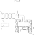
たとえば、特開平8−236298号公報に記載された装置は、導電性の材料からなる円筒容器内に高周波線路側円筒容器端面からおおよそ高周波波長のn/2倍の管軸方向位置に、円筒容器管軸に直交しかつ高周波線路方向側に円板状の高周波透過部材を設けている。そして、高周波透過部材の高周波線路方向と反対側の領域を反応処理用減圧雰囲気として高周波線路から導入されるマイクロ波帯高周波により減圧雰囲気領域に高周波プラズマ気体放電を得ている(図1)。この装置は高周波共振回路技術における円筒空洞共振技術を利用しており、エネルギー効率をあげて高密度なプラズマを得ることが可能となっている。
また、従来の高周波反応処理装置には、導波管線路からの高周波を誘電体線路に導入して誘電体線路内に高周波を広く伝播させることにより大きな面積の電場を誘電体線路の下側に形成し、これにより投影されるプラズマ形成領域の面積を大きくしているものもある。
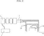
たとえば、特開昭62−5600号公報ならびに特開昭62−99481号公報に記載された装置は、導波管線路内の反応処理用減圧円筒容器の管軸に直交する端面側に平行に設けた誘電体線路を経由して誘電体線路の下側に所定間隔で対向配置された円筒容器管軸に直交した板状の透過窓を介して、マイクロ波帯高周波を導波管線路から減圧円筒反応室に導入し、反応処理用減圧円筒容器内で高周波プラズマ気体放電を得ている(図2)。この装置では誘電体線路により広げられた高周波電界からの誘電体線路下方側への漏れ電界を高周波透過窓から反応処理円筒容器部に透過することにより反応処理円筒容器の径方向に均一な面積の大きなプラズマを得ることができる。
また、従来の高周波反応処理装置においては、マイクロ波帯が出力の規定されたマグネトロン発振によるものであるために複数の発振部をもつマイクロ波帯立体回路を負荷に接続し、装置の大電力化を行う方式を採用しているものもある。
たとえば、マイクロ波帯高周波利用において大電力を負荷に導入する手法として、複数の高周波発振部ならびに導波管高周波立体回路を同一の負荷に接続する電力分割複数伝送路電力投入技術がある。単一伝送路から大電力を投入することも不可能ではないが、市場では入手の難しい大電力マグネトロンならびに特殊電源が必要となり実用的ではなく、当該技術はマイクロ波乾燥機等の分野において有効な手段として一般的に用いられている。(柴田長吉郎著「工業用マイクロ波応用技術」電気書院1993年)
また、従来の高周波反応処理装置では、一般的に高周波発振部から負荷への電力移送に関するインピーダンス整合および負荷からの反射波への対策のための技術を採用している。このような装置では、高周波線路において、結合部および負荷からの反射波の影響で高周波発振部方向に発生した反射波の反射成分を吸収するために、アイソレーターおよびインピーダンス整合器を挿入して高周波発振部に反射波が戻らないような構成が組まれている。
たとえば、高周波発振部から負荷への電力移送に関するインピーダンス整合および負荷からの反射波への対策のための技術として、高周波線路において、結合部および負荷からの反射波の影響で高周波発振部方向に発生した反射波の反射成分を吸収するために、アイソレーターおよびインピーダンス整合器を挿入して高周波発振部に反射波が戻らないような構成が組まれている(図3、柴田長吉郎著「工業用マイクロ波応用技術」電気書院1993年)。このような構成は、導波管高周波立体回路の標準としてほとんどのマイクロ波帯高周波反応処理装置に使用されている。
また、従来の高周波反応処理装置の中の高周波プラズマ装置においては、高周波発振部方向への負荷からの反射波を受けず、アイソレーターならびにインピーダンス整合器を除外して導波管高周波立体回路を簡略化かつ低コスト化し、かつ損失のない伝送路を実現する手法として、電離気体プラズマ自体が誘電体特性を有し、かつ可変インピーダンスであることを応用利用し、プラズマ負荷を高周波発振部からの電磁波の全位相波を吸収するものもある。
たとえば、高周波発振部方向への負荷からの反射波を受けず、アイソレーターならびにインピーダンス整合器を除外して導波管高周波立体回路を簡略化かつ低コスト化し、かつ損失のない伝送路を実現する手法として、本願出願人は、電離気体プラズマ自体が誘電体特性をもち、かつ可変インピーダンスであることを応用利用し、プラズマ負荷を高周波発振部からの電磁波の全位相波を吸収できる処理装置を特願2000−559714(国際出願番号 PCT/JP99/03650)において提案している。この装置は、プラズマ放電開始時を含めた負荷インピーダンスの大きな変動にも対応でき、高周波線路を極力短縮することが可能で、プラズマの安定放電を実現している。
また、従来の高周波反応処理装置には、電子レンジに代表される多重モード空洞共振器を用いたマイクロ波加熱装置がある(図4)。
この装置では回転ステラファンにより電磁波の拡散あるいは、被加熱体をターンテーブル上で回転することによって被加熱体を均一に加熱する。
また、従来の高周波反応処理装置には、セラミック焼結等に用いられる単一モード共振器を用いたマイクロ波加熱装置がある(図5)。
低誘電体損の材料を加熱する場合、多重モード共振器の装置では空洞内電界が比較的均一にはなるものの入力エネルギーが各モードに分散されるため加熱が困難になるが、この装置は、電界最大点に被処理材料を置き、入力エネルギーを集中し処理をしており、高温焼結等に利用される。
また、従来の高周波反応処理装置には、導波管線路からの高周波を誘電体線路に導入して誘電体線路内に高周波を広く伝播させることにより大きな面積の電場を誘電体線路の下側に形成し、処理材料を一度均一加熱板上に設置して処理を行い、処理材料での均一処理を達成しているものもある。
たとえば、特開2000−150136号公報に記載された装置は、マイクロ波を誘電体に照射して表面波を形成し加熱板を介して処理物を加熱している(図6)。この装置では大面積の被加熱体を均一に加熱することができる。
また、従来の高周波反応処理装置には、無反射終端形状負荷構造によって、小型かつ低コストで、反射定在波の発生がなく、高効率に導入エネルギーを負荷に投入できる液体加熱装置がある。
たとえば、特願平10−333329において本出願人により提案されている装置は、無反射終端型ブロックを液体加熱部のマイクロ波進行方向に対して、反対側に接触または近接設置している(図7)。この装置は、高周波発振部方向への負荷からの反射波を受けず、アイソレーターならびにインピーダンス整合器を除外し、導波管高周波立体回路を簡略化かつ低コスト化し、反射波の無い高効率の液体加熱を実現している。
発明の開示
本発明の目的は、大容量の高周波プラズマ生成に不可欠な装置の大電力化,プラズマの高均一化,高効率化ができかつ低コストであることを同時に満足する高周波反応処理装置を提供することにある。
本発明が解決しようとする課題は、マイクロ波帯域の高い高周波を用い、高周波結合部からの反射のない無反射状態を実現することにより導波管立体回路内から反射波対策機構部品であるアイソレーターならびに整合器を除外して、高周波結合部ならびにプラズマ負荷構造によって高周波結合部以降の負荷が無反射終端回路と等価の構造とすることである。
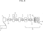
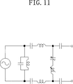
図8に示す従来技術は、電離気体プラズマ放電装置のような可変インピーダンス負荷への電力移送を行うためのインピーダンス整合および反射波対策に関する標準的な方式を採用している。図8は、この技術に係る装置におけるマイクロ波進行波と反射波の状態ならびにアイソレーターとインピーダンス整合器の機能を示している。本構成を集中定数等価回路で示したものが図9である。また、図10は、図9からプラズマ境界面を高周波終端面と考えた図であり、アイソレーターを除外した場合の等価回路図であり、図11は図10においてプラズマ発生がない状態の等価回路図である。
プラズマ負荷部において、プラズマ生成の無い状態からプラズマを発生させるためには回路終端に電離ガスが初期乖離するだけの高電圧を必要とする。高周波回路においては高電圧を得るために直列共振回路を用いることが有利であるが本回路構成では図11に示されているように終端において共振を行うためには整合器回路内の可変LあるいはCを変動させて共振点を得なければならないことを本発明者は見出した。また、共振を起こすまでの調整期間中は、発振部に反射波が帰還することを示していてアイソレーター回路の必然性を示している。
さらに、図10に示すように、プラズマ負荷生成後においては、逆L型インピーダンス整合回路が形成されているが可変インピーダンスであるプラズマ負荷においてインピーダンス変化が起こった場合には、常時追随できるような自動機能整合回路が必要であることを本発明者は見出した。
すなわち、従来技術のような構成において信頼性のある装置を実用化するには、アイソレーターと自動追随機能整合器を導波管伝送路に必要とする。この場合、伝送線路であるマイクロ波帯立体回路の物理的サイズが増加する。大幅なコスト上昇の問題があり、マイクロ波帯利用の阻害要因である。特に電力分割複数伝送路電力投入方法の従来技術を用いる場合には装置サイズは肥大化する。
従来のマイクロ波電離気体プラズマ放電装置で、インピーダンス整合および反射波対策に関する標準的な方式の従来技術と電力分割複数伝送路電力投入方法を用いて2つの高周波伝送路から同一プラズマ負荷に対し高周波電力を導入し大電力化をおこなう場合での高周波進行波と反射波の状態ならびにこれに作用するマイクロ波立体回路の各部の機能を図12に示す。本構成を集中定数等価回路で示したものが図13である。図14はプラズマ境界面を高周波終端面と考えた場合の等価回路を示したものである。
図12に示すように、整合器とプラズマ負荷間全体の領域26は個別な2つの高周波伝送路により共有されていて図14の回路図で示しているように電離プラズマ生成によって両側の回路は連動し、各々の整合器動作によってインピーダンス整合に関し相互干渉することとなる。これにより、生成プラズマの変動が発生し、プラズマ負荷部での電界不均一等の不安定性が増大することを本発明者は見出した。また、図8に示す技術の検討から、プラズマ負荷自体を高周波発振部からの電磁波の全位相波を吸収できる無反射終端構造で形成する必要があることを本発明者は見出した。さらに本技術では、大容積プラズマ生成に必要な高周波結合部における電場の拡大に対応するためのプラズマ負荷形状を形成するには構造的限界を生じ、高周波結合部において発生する反射波の問題を回避できないことを本発明者は見出した。
本発明に係る高周波反応処理装置は、誘電性材料で構成され、2つの端面により内腔を閉鎖することができる外容器と、誘電性材料で構成され、前記外容器の内側面に接さず、高周波結合部を通して飛来する高周波を受ける位置に設けられ、2つの端面により内腔を閉鎖することができる1又は2以上の内容器と、前記外容器の外面の任意の位置に設けられた1又は2以上の高周波結合部と、導電性材料で構成され、前記外容器の外面で前記高周波結合部が設けられた部分以外を被覆し、高周波線路接地電位と同電位に保たれた被覆部と、を備え、前記内容器の内腔において反応処理を行うことを特徴としている。
このように、本発明に係る高周波反応処理装置においては、誘電体により形成された外容器と、その内側に誘電体により形成されている内容器が配置されて、外容器の外面には高周波結合部が設けられ、それ以外の外面部分には接地電位に保たれた導電体の被覆部が設けられている。
これにより、外容器の容器外側の高周波結合部以外の部分は導入高周波接地電位となるよう導体被覆されているため、内容器内側の反応処理領域において多数の強電界点を持たせることができる。
また、高周波結合部を筒状側面あるいは球状側面に設けて高周波伝播線路がループ状に帰還するように、筒状あるいは球状の誘電体容器により線路が形成されるため、線路面積の大きな無限長誘電体線路を構成し、高周波導波管線路より電磁波を無限長誘電体線路方向に伝播させることができる。
これにより、無限長誘電体線路を実現することができ、複数の高周波結合部を同一誘電体線路に導入するに際し、各々の高周波結合部導入位置を調整することにより、各々の導入される高周波の相互干渉を抑制でき、同一線路内にて共振を増幅することが可能となる。その結果、共振状態によっては系全体の反射係数を減じることが可能となる。
また、複数の高周波結合部から同一負荷に電力を投入する電力分割複数伝送路電力投入によって任意に投入電力を増加できる構造としているため、大電力を投入することが可能になる。
また、導波管線路からの高周波を誘電体線路に導入して誘電体線路内に高周波を広く伝播させているため、均一で大きな電界面を誘電体線路の内側の内容器内側の反応処理領域に発生させることができ、大容積であって高均一に電力を投入できる高周波反応装置を実現できる。
また、高周波反応装置がプラズマ装置の場合においては、投入電力の増加によって内容器内側の電離気体プラズマの電子密度が上昇するにつれて電離気体プラズマの境界面は導体と同様の性質を増し、ループ上に帰還している無限長誘電体線路と電離気体プラズマ境界面とで閉鎖される領域において電磁波が反射伝播するため、電磁波伝播面積が増加して大面積に対して電界を生成することが可能となる。
また、プラズマ負荷部においてプラズマ生成の無い状態からプラズマを発生させるには、回路終端に電離ガスが乖離するだけの高電圧を必要とするが、上記のような構成をとることにより、終端側に共振回路が構成されていて高電圧が発生しプラズマの着火が容易となる。また、高周波結合部および誘電線路によって結合回路型整合器と等価の回路が構成されているため、負荷回路が発振部領域から分離されていることにより負荷変動に対して安定した回路を実現することができる。その結果、電力の投入から反射波の発振部への帰還に強く、かつ電力の負荷への投入を多くすることができる回路構成を実現できる。
【図面の簡単な説明】
図1は、従来の円筒共振型磁場付加方式のマイクロ波放電装置の放電部概略断面図および構成図である。
図2は、従来の有限長誘電体線路表面波方式のマイクロ波放電装置の放電部概略断面図および構成図である。
図3は、従来のH面貫通型チューブアプリケーター方式のマイクロ波放電装置の放電部概略断面図および構成図である。
図4は、従来の多重モード空洞共振型のマイクロ波加熱反応装置の概略断面図および構成図である。
図5は、従来の単一モード共振型のマイクロ波焼結反応装置の概略断面図および構成図である。
図6は、従来の有限長誘電体線路表面波方式におけるマイクロ波加熱反応装置の概略断面図および構成図である。
図7は、従来の無反射型のマイクロ波液体加熱反応装置の概略断面図および構成図である。
図8は、従来のH面貫通型チューブアプリケーター方式のマイクロ波放電装置におけるマイクロ波進行波と反射波の状態並びにアイソレーターとインピーダンス整合器の機能を示した図である。
図9は、従来のマイクロ波放電装置におけるマイクロ波伝送立体回路構成を集中定数等価回路で示した図である。
図10は、従来のマイクロ波放電装置におけるマイクロ波伝送立体回路構成の集中定数等価回路においてプラズマ境界面を高周波終端面と考えた場合でかつアイソレーターを除外した場合の等価回路を示した図である。
図11は、従来のマイクロ波放電装置におけるマイクロ波伝送立体回路構成の集中定数等価回路においてプラズマ放電がない場合でかつアイソレーターを除外した場合の等価回路を示した図である。
図12は、従来のマイクロ波放電装置において電力分割複数伝送路電力投入方法を用いて2つの高周波伝送路から同一プラズマ負荷に対しての高周波電力の導入による大電力化を行う場合の高周波進行波と反射波の状態並びにこれに作用するマイクロ波立体回路の各部の機能を示した図である。
図13は、従来のマイクロ波放電装置において電力分割複数伝送路電力投入方法を用いて2つの高周波伝送路から同一プラズマ負荷に対しての高周波電力の導入による大電力化を行う場合のマイクロ波伝送立体回路構成を集中定数等価回路で示した図である。
図14は、従来のマイクロ波放電装置において電力分割複数伝送路電力投入方法を用いて2つの高周波伝送路から同一プラズマ負荷に対しての高周波電力の導入による大電力化を行う場合のマイクロ波伝送立体回路構成を集中定数等価回路におけるプラズマ境界面を高周波終端面と考えた場合の等価回路を示した図である。
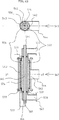
図15は、本発明に係るマイクロ波反応処理装置構造を定義する3軸立体外形図の一例を示した図である。
図16は、本発明に係るマイクロ波反応処理装置構造を定義する3軸立体外形図(図15)の内部透視図を示した図である。
図17は、本発明の装置構造でのマイクロ波反応処理装置の概略断面図および構成図である。
図18は、本発明の装置構造におけるマイクロ波伝送立体回路構成を集中定数等価回路で示した図である。
図19は、本発明の装置構造におけるマイクロ波伝送立体回路構成の集中定数等価回路において処理容器導体壁面を高周波終端面と考えた場合の等価回路を示した図である。
図20は、本発明のマイクロ波反応処理装置において電力分割複数伝送路電力投入方法を用いて2つの高周波伝送路から同一負荷に対しての高周波電力の導入による大電力化を行う場合のマイクロ波伝送立体回路構成を集中定数等価回路で示した図である。
図21は、本発明のマイクロ波反応処理装置において電力分割複数伝送路電力投入方法を用いて2つの高周波伝送路から同一負荷に対しての高周波電力の導入による大電力化を行う場合のマイクロ波伝送立体回路構成を集中定数等価回路における処理容器導体壁面を高周波終端面と考えた場合の等価回路を示した図である。
図22は、本発明に係る放電装置構造を定義する3軸立体外形図の一例を示した図である。
図23は、本発明に係る放電装置構造を定義する3軸立体外形図(図22)の内部透視図を示した図である。
図24は、本発明に係る放電装置構造を定義する3軸立体外形図の一例を示した図である。
図25は、本発明に係る放電装置構造を定義する3軸立体外形図(図24)の内部透視図を示した図である。
図26は、本発明の装置構造でのマイクロ波放電装置の放電部概略断面図および構成図である。
図27は、本発明の装置構造におけるマイクロ波伝送立体回路構成を集中定数等価回路で示した図である。
図28は、本発明の装置構造におけるマイクロ波伝送立体回路構成の集中定数等価回路においてプラズマ境界面を高周波終端面と考えた場合の等価回路を示した図である。
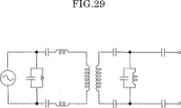
図29は、本発明の装置構造におけるマイクロ波伝送立体回路構成の集中定数等価回路においてプラズマ放電がない場合の等価回路を示した図である。
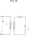
図30は、一般的な高周波誘電体共振回路の等価回路を示した図である。
図31は、一般的な高周波結合回路型整合器回路の等価回路を示した図である。
図32は、本発明のマイクロ波放電装置において電力分割複数伝送路電力投入方法を用いて2つの高周波伝送路から同一プラズマ負荷に対しての高周波電力の導入による大電力化を行う場合の高周波進行波と反射波の状態並びにこれに作用するマイクロ波立体回路の各部の機能を示した図である。
図33は、本発明のマイクロ波放電装置において電力分割複数伝送路電力投入方法を用いて2つの高周波伝送路から同一プラズマ負荷に対しての高周波電力の導入による大電力化を行う場合のマイクロ波伝送立体回路構成を集中定数等価回路で示した図である。
図34は、本発明のマイクロ波放電装置において電力分割複数伝送路電力投入方法を用いて2つの高周波伝送路から同一プラズマ負荷に対しての高周波電力の導入による大電力化を行う場合のマイクロ波伝送立体回路構成を集中定数等価回路におけるプラズマ境界面を高周波終端面と考えた場合の等価回路を示した図である。
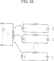
図35は、一般的な伝送線と結合した空洞共振器における高周波結合部の等価回路を示した図である。
図36は、本発明の第一実施例での高周波電離気体プラズマ装置放電部構成の鉛直中心部断面図および、y1−y2における水平断面図である。
図37は、本発明の第二実施例での高周波電離気体プラズマ装置放電部構成の鉛直中心部断面図および、y1−y2における水平断面図である。
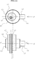
図38は、本発明の第三実施例での高周波電離気体プラズマ装置放電部構成の鉛直中心部断面図および、y1−y2における水平断面図である。
図39は、本発明の第一実施例の変形例での高周波電離気体プラズマ装置放電部構成の鉛直中心部断面図および、y1−y2における水平断面図である。
図40は、本発明の第一実施例の変形例での高周波電離気体プラズマ装置放電部構成の鉛直中心部断面図および、y1−y2における水平断面図である。
図41は、本発明の第一実施例の変形例での高周波電離気体プラズマ装置放電部構成の鉛直中心部断面図および、y1−y2における水平断面図である。
図42は、本発明の第一実施例の変形例での高周波電離気体プラズマ装置放電部構成の鉛直中心部断面図および、y1−y2における水平断面図である。
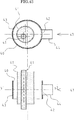
図43は、図42に示す実施例の変形例での高周波電離気体プラズマ装置放電部構成の鉛直中心部断面図および、y1−y2における水平断面図である。
図44は、本発明の第一実施例の変形例での高周波電離気体プラズマ装置放電部構成の鉛直中心部断面図および、y1−y2における水平断面図である。
図45は、本発明の第一実施例の変形例での高周波電離気体プラズマ装置放電部構成の鉛直中心部断面図および、y1−y2における水平断面図である。
図46は、本発明の第一実施例の変形例での高周波電離気体プラズマ装置放電部構成の鉛直中心部断面図および、y1−y2における水平断面図である。
図47は、本発明の第一実施例の変形例での高周波電離気体プラズマ装置放電部構成の鉛直中心部断面図および、y1−y2における水平断面図である。
図48は、本発明の第一実施例の変形例での高周波電離気体プラズマ装置放電部構成の鉛直中心部断面図および、y1−y2における水平断面図である。
図49は、本発明の第一実施例の変形例での高周波電離気体プラズマ装置放電部構成の鉛直中心部断面図および、y1−y2における水平断面図である。
図50は、本発明の第一実施例の変形例での高周波電離気体プラズマ装置放電部構成の鉛直中心部断面図および、y1−y2における水平断面図である。
図51は、本発明の第一実施例の変形例での高周波電離気体プラズマ装置放電部構成の鉛直中心部断面図および、y1−y2における水平断面図である。
図52は、本発明の第一実施例の変形例での高周波電離気体プラズマ装置放電部構成の鉛直中心部断面図および、y1−y2における水平断面図である。
図53は、本発明の第四実施例での反応処理部構成の鉛直中心部断面図および、y1−y2における水平断面図である。
図54は、本発明の第五実施例での反応処理部構成の鉛直中心部断面図および、y1−y2における水平断面図である。
図55は、本発明の第六実施例での反応処理部構成の鉛直中心部断面図および、y1−y2における水平断面図である。
図56は、図42に示す変形例での反応処理部構成の鉛直中心部断面図および、y1−y2における水平断面図である。
図57は、本発明の第六実施例の変形例での反応処理部構成の鉛直中心部断面図および、y1−y2における水平断面図である。
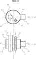
図58は、本発明の第四実施例の変形例での反応処理部構成の鉛直中心部断面図および、y1−y2における水平断面図である。
図59は、本発明の第四実施例の変形例での反応処理部構成の鉛直中心部断面図および、y1−y2における水平断面図である。
図60は、本発明の第四実施例の変形例での反応処理部構成の鉛直中心部断面図および、y1−y2における水平断面図である。
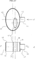
図61は、本発明の第四実施例の変形例での反応処理部構成の鉛直中心部断面図および、y1−y2における水平断面図である。
図62は、本発明の装置構造でのマイクロ波反応処理装置の概略断面図および構成図である。
図63は、本発明の第七実施例での反応処理部構成の鉛直中心部断面図および、y1−y2における水平断面図である。
図64は、本発明の第八実施例での反応処理部構成の鉛直中心部断面図および、y1−y2における水平断面図である。
図65は、本発明の第九実施例での反応処理部構成の鉛直中心部断面図および、y1−y2における水平断面図である。
図66は、本発明の第十実施例での反応処理部構成の鉛直中心部断面図および、y1−y2における水平断面図である。
図67は、本発明の第十実施例の変形例での反応処理部構成の鉛直中心部断面図および、y1−y2における水平断面図である。
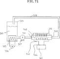
図68は、本発明の第十一実施例の廃水処理方法および処理システムを示す概略構成図である。
図69は、本発明の第十一実施例の変形例の廃水処理部構成の鉛直中心部断面図および、y1−y2における水平断面図である。
図70は、本発明の第十一実施例の変形例の廃水処理方法および処理システムを示す概略構成図である。
図71は、本発明の第十一実施例の変形例の廃水処理方法および処理システムを示す概略構成図である。
発明を実施するための最良の形態
添付図面に従い、以下に本発明に係る実施の形態について説明する。
課題が解決されるための具体的な装置の構造について、添付図面に従い説明する。
均一で大きな電界面を処理領域に発生させるために、導波管線路からの高周波を誘電体線路に導入して誘電体線路内に高周波を広く伝播させることによって、大きな面積の電場を誘電体線路の下側に形成することは有効である。しかしながら、誘電体線路が終端をもつ有限長誘電体線路である限り線路終端からの反射により不確定な定在波が形成されるため、有限誘電体線路の形状、厚み等に工夫を生じかつ導波管線路において、アイソレーターおよびインピーダンス整合器回路の設置が必要となる。
さらに、大きな電力を導入するために複数の高周波結合部から同一負荷に電力を投入する電力割当複数伝送路電力投入を行おうとすると各々の線路における高周波結合部位置から負荷までの距離が均等でなく有限長線路終端からの反射定在波が異なることから各線路毎にインピーダンス変化に常時追随できる自動インピーダンス整合器による反射定在波を制御する必要が生じる。その結果、装置の構造が高価なものとなり、高周波伝送路が導波管を用いるために装置が大型化して装置設計上に制約を与える。また、伝送損失による装置の効率低下をもたらす。
本発明においては、誘電体線路を高周波伝播がループ状に帰還する線路とすることにより、等価回路上線路を無限長とし、誘電体線路に高周波を循環させる。また、帰還線路長自体を導入される電磁波の1/4波長の整数倍とすることによって、伝送線路共振を起こし、共振状態により反射係数を減じる。
線路共振を行うためには共振線路長は1/2波長の整数倍であれば条件は満足するが、導入されるモードがTMモードであるかTEモードであるかによって電界ピーク位置が1/4波長長さずれるために線路長を1/4波長の整数倍とする。
また、線路長が1/4波長の整数倍でありかつループ状に帰還していれば1/4波長インピーダンス変成器としても作動することから負荷側に並列あるいは直列リアクタンスが挿入されると整合器としても作動することになって発振回路への反射を低減することもできる。
また、複数の高周波結合部を同一誘電体線路に導入するに際し、上記のような無限長誘電体線路では各々の高周波結合部導入位置を調整することにより、導入される高周波の相互干渉を抑制でき、同一線路内にて共振を増幅することが可能である。その結果、共振状態によっては系全体の反射係数を減じることが可能となる。
線路面積の大きな無限長誘電体線路を構成するには誘電体による筒状あるいは球状の誘電体容器により線路を形成すれば実現できる。高周波結合部を筒状側面あるいは球状側面に設けて高周波伝播線路がループ状に帰還するように容器を構成すればよく、高周波導波管線路より無限長誘電体線路方向に電磁波が伝播するように高周波結合部を設ける構成とすればよい。
さらに、無限長誘電体線路において線路面の片側を導入高周波電力接地電位の導体で被覆し、接地電位側線路面の反対側において1/4波長の整数倍距離の位置に抵抗である処理領域を生成する。これにより、誘電体線路からの垂直方向に発生する漏洩電界の多数の強電界点がこの処理領域に発生し、負荷に対し効率の高い入力エネルギーの集中が行える。
さらに、負荷までの距離が無限長誘電体線路から1/4波長の整数倍であることから、この構成自体が漏洩電磁波の1/4波長インピーダンス変成型整合器としても作動して系全体の反射係数を減じることが可能となる。
また、無限長誘電体線路の全ての線路にわたって、上記のように接地電位側線路面の反対側において1/4波長の奇数倍距離の位置に抵抗である負荷領域を生成するような形状においては、伝送線路の共振としては並列共振回路特性と等価となる。この結果、系全体として大きな電流を負荷に投入でき、大電力の負荷投入が容易になり、負荷吸収効率が増加する。
また、導体の境界面を処理領域の内側に形成することにより、ループ上に帰還している無限長誘電体線路と導体面とで閉鎖される導体でない材料の処理領域において電磁波が反射伝播する。これにより、さらに電磁波伝播面積が増加して大面積に対して電界を生成することが可能となる。
以上のことから、以下のように装置を構成すれば上記の条件は満足される。すなわち装置は、誘電体による筒状あるいは球状の誘電体面線路を構成し、当該誘電体線路を無限線路と等価にするために高周波結合部を筒状側面あるいは球状側面に設けて高周波伝播線路がループ状に帰還する無限長誘電体線路を構成する。また、帰還長を少なくとも導入される高周波の1/4波長の整数倍とし、さらに、無限長誘電体線路である容器外側の高周波結合部以外の部分を導入高周波接地電位となるよう導体被覆する。また、導体面と無限長誘電体線路の境界面から導入される高周波波長の1/4波長長さを隔てた距離の部分に少なくとも一部の面をもつ処理材料容器を構成し、必要に応じて処理材料容器の内側に導体面をもつ構成とする。
図15は、本発明に係る装置構造を定義する3軸立体外形図、図16は図15の立体の内部透視図である。他の記号と判別するために図面符号は■■内に示す。
外容器Va■240■の外側面の任意な位置を導波管線路からの高周波導入結合部■242■を少なくとも1つ以上設け導波管線路から導入し高周波■247■を誘電体線路である誘電体外容器Va■240■の誘電体に伝播させる。外容器Va■240■は、対称軸面Sz1■232■に対称であって内腔を持ち、かつSz1と直交しさらに高周波結合部■242■と交差する面Sx1■246■により切断された断面形状におけるその外郭線が連続曲線であり、さらにZ軸方向距離がL1■234■の2つの端面(a1■236■およびa2■237■)により内腔を閉鎖することができ、誘電体で構成される。L1は、外容器の両端面を結ぶ軸の長さである。
少なくとも電磁波の伝播方向が結合部近傍において面Sx1■246■により切断される断面形状における内郭線に沿って電磁波が伝播するような電磁波モードにより高周波を結合する。ループ状に閉鎖している内郭線の長さが少なくとも導入される高周波波長の1/4波長の整数倍となるように、外容器Va■240■を構成する。
さらに、外容器Va■240■外面の高周波導入結合部以外の部分を高周波線路接地電位と同電位の導電体■243■によって被覆する。
また、高周波結合部■242■においては、導波管線路と外容器Va■240■面との接続角により、あるいは外容器Va■240■の曲面自体により、あるいは外容器Va■240■と接続する誘電体の形状により導波管線路からの電磁波の電界が誘電体面に対して垂直でなく面方向に拡散するような構造あるいは導入電磁波モードを選択することにより効率よく導入電磁波を誘電体線路に導入し、高周波結合部における反射発生を抑制する構造とする。
被処理材料の処理領域外郭となる内容器Vb■241■は、面Sz1のZ軸と平行な線分を含む面Sz2■233■あるいは面Sz1のうちの少なくとも1つ以上の面に対称で内腔を有する。さらに、少なくともZ軸方向距離L1の端面(a1およびa2)を各々含む2つの面により内腔を閉鎖することができ、誘電体で構成される。
内容器Vb■241■を外容器Va■240■の内側面に接することなく挿入するが、面Sx1■246■により切断される断面を持たなければならない。さらに当該断面形状の少なくとも一部において外容器Va■240■断面の外郭線と内容器Vb■241■断面の内郭線との距離が導入される高周波の1/4波長の整数倍となるように構成する。
2つ以上の内容器Vb■241■を外容器Va■240■内に相互に内腔を重複しないように挿入して複数の処理領域を作成してもよい。また、内容器Vb■241■の内側に少なくともZ軸方向距離L1の端面(a1およびa2)を各々含む2つの面により内腔を閉鎖することができる内容器Vcを内容器Vbに接することなく配置し、被処理材料が内容器Vbと内容器Vcで狭窄される領域を処理領域としてもよい。
また、被処理材料の処理領域の内側を構成する内容器Vc■256■の少なくとも外側面あるいは内側面を導体面として誘電体線路である誘電体外容器Va■240■からの漏洩電界からの電磁波を反射させ、導電体■243■との間において反射伝播させて、処理領域を通過する電磁波により効率よく反応処理を行う。
また、上記と同様な効果を得るために、内容器Vc■256■が誘電体の場合においては、内容器Vc■256■を減圧として内部に電離プラズマを発生させて電離プラズマのプラズマ境界面を導電体■243■と等価の意義で用いることもできる。
また、被処理材料の処理領域の内側を構成する内容器Vc自体に反応処理のために加熱あるいは冷却の別のエネルギー源を設けて内容器Vcの外側の処理領域の補助反応源として用いることも可能となる。
また、外容器Va■240■および内容器Vb■241■は異なる誘電体材料による多層構造であってもかまわない。異なる材質の誘電体層を用いると誘電体層間において電磁波の屈折現象が生じるために材質の選定が正しければ、電磁波を誘電体層の面方向に拡散し電界面を大きくすることになる。
また、外容器Vaの内側面あるいは内容器Vbの外側面を凹凸形状あるいは、研磨等により表面を粗くすることによって電磁波を面方向に誘電体層拡散し電界面を大きくすることになる。
処理領域でない外容器Va■240■と内容器Vb■241■で狭窄される領域において、気体冷却あるいは誘電率の低い液体を用いた液体冷却を行うことにより処理領域を形成する内容器Vb■241■の壁面を冷却し処理反応温度の制御が可能となる。
また、処理領域を形成する内容器Vbあるいは内容器Vbと内容器Vcで狭窄される領域のZ軸方向を閉じる面が導体面でありZ軸方向距離が導入される高周波波長の1/4波長の整数倍となるように構成した場合、内容器Vbと内容器Vcの容器形状ならびに寸法を適正化することにより空洞共振器を構成し共振状態を最適化することが可能となる。
また、処理領域に対して、永久磁石あるいは電磁石によりZ軸方向に磁場を形成するように構成し、さらに反応速度を上昇させることも可能となる。
また、内容器Vbの容器内部で生成されるマイクロ波電界部に対して、永久磁石あるいは電磁石によりZ軸方向に磁場を形成するように構成して、さらに電界密度を上昇させることも可能となる。
以上のような構成のマイクロ波反応処理装置における反射波抑制機構とインピーダンス整合機構について、添付図面に従い説明する。
図17は、上記の装置構造を高周波伝送系も含めて示した装置構成概略図である。
高周波発振部■202■は、マグネトロンが内蔵されていて、高圧電源■201■の高電圧によって所定の高周波電磁波を励起発振する。電磁波は矩形導波管■203■を経由して高周波結合部■223■にて誘電体外容器Va■240■と結合し誘電体線路である外容器Va■240■に導入される。高周波結合部以外の外容器Va外側面は、導波管線路と同電位接地された導体で被覆されている。そのため、導入された電磁波は、容器側面において無限長誘電体線路として機能する外容器Va■240■の側面方向に拡散伝播し、表面波によって容器内側に漏洩電界を生じる。
表面波電磁波は誘電体外容器Va■240■と処理容器側壁でもある誘電体内容器Vb■241■で狭窄される領域に導入され、高周波進行波■221■と反射波■222■による定在波を立てると共に、誘電体内容器Vbn■241■内部に導入されてそのエネルギーは被処理体負荷内に吸収される。
図17に示すように、本構成においては伝送経路にインピーダンス整合器を設けていないにもかかわらず、マグネトロン発振部に支障をきたさないのは、系全体として負荷に対して整合が取れていて導波管■203■において反射波が存在しないためである。
図18は、図17の構成を集中定数等価回路で示した図である。また、図19は、図18で容器導体面を高周波終端面と考えて簡略化された等価回路を示す図である。
図18に示すように、本構成は全体回路としては一般的な誘電体共振回路が2つ結合し、共振器に入力線路と出力線路が結合した2結合共振器回路となっている。高周波結合部を示す回路領域■223■と内容器Vb結合部を示す回路領域■228■の間に1/4波長インピーダンス変成器型整合回路が形成された形である。
2結合共振器回路においては、入力結合線路のQが、出力結合線路のQの約二分の一となる条件が満たされると無反射となる(岡田文明著「マイクロ波工学」学献社1993年)。したがって、装置の設計最適化により無反射が達成される。
図18に示すように、本構成では処理負荷部において終端側に共振回路■219■が構成されていて装置のエネルギー効率が高い。また、高周波結合部および誘電線路によって、図19に示すような結合回路型整合器と等価の回路が構成されていて、負荷回路が発振部領域から分離されており、本装置が負荷変動に強いことを示している。
さらに、図19に示すように、結合整合回路と1/4波長インピーダンス変成器型整合回路とにより変形のπ型整合器が形成されており、整合範囲を多く取れる回路構成である。また、1/4波長インピーダンス変成器型整合回路が負荷に対して並列共振回路を構成するために、負荷における電流値を増加しやすく電力効率をあげられるような回路構成となっている。
すなわち、電力の投入から反射波の発振部への帰還に強く、かつ電力の負荷への投入を多くすることができる回路構成である。
この技術を用いて電力分割複数伝送路電力投入方法による2つ以上の高周波伝送路から同一負荷に対して高周波電力を導入し大電力化を行う場合の集中定数等価回路で示した図が図20であり、処理容器導体面を高周波終端面と考えた場合の簡略化した等価回路を示した図が図21である。
図20に示すように、負荷は個別な2つの高周波伝送路により共有されている。図21に示すように、負荷部分の領域は両発振部からの結合回路型整合回路で分離されており、また結合回路以降の負荷部分全体が並列共振回路を構成している。この状態は伝送線路と結合した空洞共振器回路の1次側と2時側が反転した構成と等価であり複数伝送路電力投入によっても発振部と負荷部分において相互干渉の無い回路構成となることを示している。
上記のように、負荷全体部が並列共振回路を構成することにより終端負荷での電流値を増加することが容易となる。これにより、負荷での電力消費効率が増加することとなり大電力投入も可能となる。
以上のような構成によって、装置の性能条件と高周波伝送回路条件を解決する手法との間において相互に矛盾がない高周波反応装置が実現する。その装置の導波管線路には、アイソレーターおよびインピーダンス整合器回路等を必要とせず、複数の高周波結合部から回路上において相互干渉することなく同一負荷に電力が投入でき。任意に投入電力を増加でき、かつ均一で大きな電界面を反応処理領域に発生させる。このようにして、伝送損失が小さく、負荷における電力消費効率も高く、かつ小型で低コスト化可能な大容積対応のマイクロ波反応装置が実現する。
添付図面に従い、以下に本発明に係る実施の形態1の高周波反応処理装置がプラズマ発生装置であるものについて説明する。
誘電体による筒状あるいは球状の誘電体面線路を構成する。誘電体線路を無限線路と等価にするため、高周波結合部を筒状側面あるいは球状側面に設ける。帰還長を少なくとも導入される高周波の1/4波長の整数倍とする。さらに、無限長誘電体線路である容器外側の高周波結合部以外の部分を導入高周波接地電位となるよう導体被覆する。導体面と無限長誘電体線路の境界面から導入される高周波波長の1/4波長長さを隔てた距離の部分に少なくとも一部の面をもつ減圧容器ともなる誘電体で構成される電離気体プラズマ減圧容器を構成する。
図22は、本発明に係る放電装置構造を定義する3軸立体外形図、図23は、図22の立体の内部透視図である。また、図24および図25は、図22の形状の一部を変形したものを示した図である。他の記号と判別するために図面符号は■■内に示す。
以下のような外容器Va■40■の外側面の任意な位置に導波管線路からの高周波導入結合部■42■を少なくとも1つ以上設け導波管線路から導入される高周波■47■を誘電体線路である誘電体外容器Va■40■の誘電体に伝播させる。外容器Va■40■は、対称軸面Sz1■32■に対称であって内腔を持つ。たとえば、楕円柱や楕円体などの形状とすることができる。これにより、電磁波を外容器の周囲方向について伝播させやすくすることができる。さらに、外容器Va■40■は、面Sz1と直交しさらに高周波結合部■42■と交差する面Sx1■46■により切断された断面形状における外郭線が連続曲線である。さらに、外容器Va■40■は、Z軸方向距離がL1■34■の2つの端面あるいは端点(a1■36■およびa2■37■)により内腔を閉鎖することができ、誘電体で構成される。L1は、外容器の両端面を結ぶ軸の長さである。
少なくとも電磁波の伝播方向が結合部近傍において面Sx1■46■により切断される断面形状における内郭線に沿って電磁波が伝播するような電磁波モードにより、高周波の結合が行われる。外容器Va■40■は、ループ状に閉鎖している当該内郭線の長さが、少なくとも導入される高周波波長の1/4波長の整数倍となるように構成される。
さらに、外容器Va■40■外面の高周波導入結合部以外の部分を高周波線路接地電位と同電位の導電体■43■によって被覆する。
また、高周波結合部■42■は、以下のような構造とする。すなわち、導波管線路と外容器Va■40■面との接続角により、あるいは外容器Va■40■の曲面自体により、あるいは外容器Va■40■と接続する誘電体の形状により導波管線路からの電磁波の電界が誘電体面に対して垂直でなく面方向に拡散するような構造とする。あるいは、導入電磁波モードを選択することにより効率よく導入電磁波を誘電体線路に導入し、高周波結合部における反射発生を抑制する構造とする。
電離気体プラズマ形成領域となる内容器Vbn(nは整数)■41■は減圧にできる容器であって、少なくとも一つ以上の対称軸面Sz2■33■に対称で内腔を持ちZ軸方向距離がL2■35■の2つの端面あるいは端点(b1■38■およびb2■39■)により内腔を閉鎖することができる誘電体で構成される。L2は、内容器の両端面を結ぶ軸の長さである。
内容器Vbn(nは整数)■41■を外容器Va■40■の内側面に接することなく挿入するが、面Sx1■46■により切断される断面を持たなければならない。さらに、断面形状の少なくとも一部において外容器Va■40■断面の外郭線と内容器Vbn■41■断面の内郭線との距離が導入される高周波の1/4波長の整数倍となるように構成する。
外容器の外側面と内容器の内側面との距離を一定にすることで、電磁波を円管周囲方向に伝播し易くすることができる。
2つ以上の内容器Vbn■41■を外容器Va■40■内に相互に内腔を重複しないように挿入して複数の電離気体プラズマ形成領域を作製してもよい。また、2つ以上の内容器Vbn■41■を相互に接しないように多重に挿入して内容器Vbn1の内側と内容器Vbn2の外側で狭窄される領域を減圧として電離気体プラズマ形成領域としてもよい。
図24および図25は、図22の外容器Va■40■の外側面が面状である装置を示す図である。また、外容器Va■40■は球状であってもよい。
また、外容器Va■40■および内容器Vbn■41■は異なる誘電体材料による多層構造であってもよい。異なる材質の誘電体層を用いると誘電体層間において電磁波の屈折現象が生じるために材質の選定が正しければ電磁波を誘電体層の面方向に拡散し電界面を大きくすることになる。
また、外容器Vaの内側面あるいは内容器Vbnの外側面を凹凸形状あるいは、研磨等により表面を粗くすることによって電磁波を面方向に誘電体層拡散し電界面を大きくすることになる。
電離気体プラズマ形成領域でない外容器Va■40■と内容器Vbn■41■で狭窄される領域、2つ以上の内容器Vbn■41■を相互に接しないように多重に挿入した場合における最内部の内容器Vbnの内側領域または内容器Vbn同士で狭窄されていてかつ電離気体プラズマ形成領域でなく減圧となっていない領域において、気体冷却あるいは誘電率の低い液体を用いた液体冷却を行うことにより、電離気体プラズマ領域を形成する内容器Vbn■41■の壁面を冷却しプラズマで生成した活性種の壁面再結合を抑制し、プラズマ処理の効率化を増加することが可能となる。
また、外容器Va■40■のa1■36■およびa2■37■と内容器Vbnのb1■38■およびb2■39■が導体面でありかつa1とb1、a2とb2の双方が共通な面でかつZ軸方向距離L1■34■およびL2■35■が同じ距離の場合において、Z軸方向距離L1=L2を導入される高周波波長の1/4波長の整数倍となるように構成した場合、内容器Vbnの容器形状ならびに寸法を適正化することにより空洞共振器を構成し内容器Vbnの容器内部で生成される電離気体プラズマの共振状態を最適化することが可能となる。
また、内容器Vbnの容器内部で生成される電離気体プラズマに対して、永久磁石あるいは電磁石によりZ軸方向に磁場を形成するように構成し電子サイクロトロン状態を生成して、さらにプラズマ密度を上昇させることも可能となる。
以上のような構成の高周波電離プラズマ気体放電装置における反射波抑制機構とインピーダンス整合機構について、添付図面に従い説明する。
図26は装置構造を高周波伝送系も含めて示した装置構成概略図である。
高周波発振部■2■はマグネトロンが内蔵されていて、高圧電源■1■の高電圧によって所定の高周波電磁波を励起発振する。電磁波は矩形導波管■3■を経由して高周波結合部■23■にて誘電体外容器Va■40■と結合し誘電体線路である外容器Va■40■に導入される。高周波結合部以外の外容器Va外側面は導波管線路と同電位接地された導体被覆されているために、導入された電磁波は容器側面において無限長誘電体線路として機能する外容器Va■40■の側面方向に拡散伝播し、表面波によって容器内側に漏洩電界を生じる。
上記の表面波電磁波は誘電体外容器Va■40■と真空容器■12■側壁でもある誘電体内容器Vbn■41■で狭窄される領域に導入され、高周波進行波■21■と反射波■22■による定在波を立てると共に、内部が減圧されていて処理ガスが導入されている誘電体内容器Vbn■41■内部に導入されて電離気体プラズマ負荷■15■を生成し、そのエネルギーはプラズマ負荷内に吸収される。
図26に示すように、本構成においては伝送経路にインピーダンス整合器を設けていないにもかかわらず、電離気体プラズマを発生することが可能でかつマグネトロン発振部に支障をきたさないのは、系全体としてプラズマ負荷に対して整合が取れていて導波管■3■において反射波が存在しないためである。
図27は、図26の構成を集中定数等価回路により示す図である。また、図28は図27からプラズマ境界面を高周波終端面と考えた場合の等価回路であり、図29はプラズマ発生がない状態の等価回路である。
図27において、本構成は全体回路としては図30に示した一般的な誘電体共振回路が2つ結合し、共振器に入力線路と出力線路が結合した2結合共振器回路となっている。高周波結合部を示す回路領域■23■と内容器Vbn結合部を示す回路領域■28■の間に1/4波長インピーダンス変成器型整合回路が形成された形である。
2結合共振器回路においては入力結合線路のQが出力結合線路のQの約二分の一となる条件が満たされると無反射となる(岡田文明著「マイクロ波工学」学献社1993年)ことから装置の設計最適化により無反射が達成される。
プラズマ負荷部においてプラズマ生成の無い状態からプラズマを発生させるには、回路終端に電離ガスが乖離するだけの高電圧を必要とするが、図29に示されているように本構成では終端側に共振回路が構成されていて高電圧が発生しプラズマの着火が容易であることとなり、また高周波結合部および誘電線路によって図31に示したような結合回路型整合器と等価の回路が構成されており、負荷回路が発振部領域から分離されていることにより負荷変動に強いことを示している。
さらに、図28に示すようにプラズマ負荷生成後においては、結合整合回路と1/4波長インピーダンス変成器型整合回路とにより変形のπ型整合器が形成されていて整合範囲を多く取れる回路構成である。1/4波長インピーダンス変成器型整合回路がプラズマ負荷発生により随時変化する可変インピーダンス回路となり並列共振回路を構成するために、プラズマ負荷においてインピーダンス変化が起こった場合にも負荷における電流値を増加しやすく常時追随でき、かつ電力効率をあげられるような回路構成となっている。
すなわち、本発明の構成は電力の投入から負荷におけるプラズマ発生に至る経過時間において、本回路は負荷においてプラズマの瞬時発生が容易で発生時の反射波の発振部への帰還に強く、かつプラズマ負荷生成後は負荷インピーダンスの変化に対して随時に整合がとれかつ電力の負荷への投入を多くすることができる構成をとる。
この技術を用いて、電力分割複数伝送路電力投入方法による2つ以上の高周波伝送路から同一プラズマ負荷に対して高周波電力を導入し、大電力化を行う場合の高周波進行波と反射波の状態ならびにこれに作用するマイクロ波立体回路を図32に示す。本構成を集中定数等価回路で示した図が図33であり、プラズマ境界面を高周波終端面と考えた場合の等価回路を示した図が図34である。
図32に示すように、プラズマ負荷は個別な2つの高周波伝送路により共有されている。図34に示すように、負荷部分の領域は電離プラズマ生成時においても両発振部からの結合回路型整合回路で分離されており、また結合回路以降の負荷部分全体が並列共振回路を構成している。この状態は、図35に示した伝送線路と結合した空洞共振器回路の1次側と2時側が反転した構成と等価であり、複数伝送路電力投入によっても発振部と負荷部分において相互干渉の無い回路構成となることを示している。
上記のように、負荷全体部が並列共振回路を構成することにより終端負荷での電流値を増加することが容易となる。その結果、終端プラズマ負荷での電力消費効率が増加することとなり大電力投入も可能となる。
以上のような構成によって、放電装置の性能条件と高周波伝送回路条件を解決する手法との間において相互に矛盾がないプラズマ装置が実現する。そのプラズマ装置は、導波管線路において、アイソレーターおよびインピーダンス整合器回路等を必要としない。また、複数の高周波結合部から回路上において相互干渉することなく同一負荷に電力が投入でき任意に投入電力を増加できる。さらに、均一で大きな電界面を電離プラズマ生成域に発生さる。その装置の伝送損失は小さく、プラズマ負荷における電力消費効率は高い。このように、小型で低コスト化可能な大容量対応のプラズマ装置が実現する。
以下に、本発明に係る実施の形態1の具体的な実施例として、第一から第三までの実施例およびその変形例を説明する。
図36は本発明の第一実施例の高周波電離気体プラズマ装置放電部の鉛直中心部断面図および、y1−y2における水平断面図である。
図36に示すように、高周波■47■が2つのマイクロ波発振部から発振され、それぞれ導波管高周波線路■44■を経て処理真空容器■12■を構成する本発明の装置の放電部に導入される。処理真空容器■12■は誘電体内容器Vbn■41■である円筒形の内容器石英管■55■と上部および下部のアルミ製真空容器壁■59■とアルミ製ドア試料台■57■から構成されていてオーリング■58■により真空シールされている。真空容器壁■59■には、排気減圧用の減圧排気口■56■が設けられている。プラズマ化されるガスは処理ガス入路■20■より流量を制御しつつ導入される。
本発明によるプラズマ発生までの過程を概説する。処理試料を大気中にてドア試料台■57■上に設置した後、ドア試料台■57■を上昇させて下部真空容器壁■59■にてオーリング接触シール接続する。真空容器■12■を減圧し、所定の処理ガスを処理ガス入路■20■より導入する。高周波進行方向■47■を進行方向とする高周波電磁波を導入することにより、プラズマ境界面■16■をもつ高周波電離気体プラズマが真空容器■20■内に発生する。
導波管高周波線路■44■は、誘電体外容器Va■40■の外側面に接続されている。誘電体外容器Va■40■は、外容器フッ素樹脂膜層■53■で外側面を被覆した外容器石英管■54■により構成される。外容器フッ素樹脂膜層■53■の外側面は導波管高周波線路■44■が接続されている部分以外は導波管高周波線路■44■と同電位のアルミ製被覆導体■43■によって被覆されている。さらに、被覆導体■43■はアルミ製真空容器壁■59■とも電気的に接続している。
本実施例においては、誘電体内容器Vbn■41■は誘電体内容器Vbn■41■の内側面から誘電体外容器Va■40■の外容器フッ素樹脂膜層■53■の外側面までの距離が導入される高周波の1/4波長となるように同軸状に誘電体外容器Va■40■の内部に配置されている。
また、誘電体外容器Va■40■と誘電体内容器Vbn■41■を冷却させる目的で、誘電体外容器Va■40■と誘電体内容器Vbn■41■で狭窄される領域に下部真空容器壁■59■の冷却媒体入路■71■から気体あるいは誘電率の小さな液体を流入させて上部真空容器壁■59■の冷却媒体出路■72■から排出する構造となっている。
高周波導入結合部■42■は、導波管高周波線路■44■と誘導体外容器Va■40■を接続しており、高周波■47■は高周波導入結合部■42■を介して誘電体外容器Va■40■を線路として伝播する。通常、高周波■47■の電磁波モードにより電界方向は異なるが、本実施例ではTM11モードを使用して円管である誘電体外容器Va■40■の円管周囲方向に電磁波が伝播するように電界方向をとり、電磁波が円管側面をループ状に帰還する無限長誘電体線路を形成している。
誘電体外容器Va■40■の水平断面における内郭線の長さは導入される高周波の1/4波長の整数倍となるように設計されている。これにより、誘電体外容器Va■40■の円周方向を誘電体線路として伝播する高周波■47■は伝送線路共振する。また、誘電体外容器Va■40■の外側面は被覆導体■43■により被覆されている。これにより、電磁波は外側に漏れることはなく、漏洩電界を形成する表面波が誘電体外容器Va■40■の内径方向に線路に沿って幅広く発生する。また、被覆導体■43■は接地電位に保たれている。これにより、その導体表面の内側に導入される表面波の1/4波長の整数倍の位置に多数の高電界点がループ状に幅広く発生する。
上記のように、真空容器■12■の壁面を構成する誘電体内容器Vbn■41■の内側面位置は上記表面波の高電界点と一致する。これにより、高周波■47■の導入から瞬時に容易に真空容器■12■内に電離気体プラズマが発生させることができる。
電離気体プラズマが発生すると、プラズマ境界面■16■が誘電体内容器Vbn■41■の内側に形成される。電離気体プラズマ自体が可変インピーダンスをもつため、表面波の一部は電離気体プラズマに吸収され、また表面波の他の一部はプラズマ境界面■16■により反射されることになる。反射された波は被覆導体■43■により被覆された誘電体外容器Va■40■と誘電体内容器Vbn■41■およびプラズマ境界面■16■により形成される領域を交互に反射伝播する。この領域での高周波の線路インピーダンスは電離気体プラズマのインピーダンスによって連動して変化する。そして、この領域は1/4波長インピーダンス変成器整合回路を形成する。これにより、電離気体プラズマに連動し共振が生じる。その結果、線路とプラズマ負荷との間でインピーダンス整合がとれて、最終的には電磁波エネルギーが効率よくプラズマ負荷に吸収される。
また、導入電力の増加に伴い、プラズマ密度が上昇してプラズマ境界面■16■が導体に近い性質を帯び始める。そして、上記1/4波長インピーダンス変成器線路において反射定在波が増加しても、線路の容量特性が増加し全体として並列共振回路を形成する。このため、反射定在波の増加はプラズマ負荷に対して電流値を増加させる方向に働き、プラズマ電離効率が上昇する。
以上により、反射波が導波管高周波線路■44■に帰還することが無く、発振側から負荷を見た場合無反射状態が実現する。
また、真空容器■12■は全体としてプラズマ負荷のない場合には円筒空洞共振器の構造であり、またプラズマ負荷がある場合には誘電体共振器となる構造である。このために、負荷において電力を効率よく吸収することができる。
図36に示すように、複数の導波管高周波線路■44■から高周波■47■を導入する場合であっても、定在波は1/4波長インピーダンス変成器整合回路に相当する領域に閉じ込められる。これにより、複数の発振部は相互に干渉することなく電力を負荷に注入でき、装置の大電力化が実現する。
ここで、本実施例に係る装置の具体的な寸法および容量を示す。高周波■47■は2.45GHz高周波であり、TM11モードで最大出力1Kwである。高周波結合部■42■部は幅70ミリ高さ130ミリの開口部において、誘電体外容器Va■40■と接している。誘電体外容器Va■40■は厚み4ミリのPTFE製外容器フッ素樹脂膜層■53■で外側面を被覆した外径150ミリ肉厚3ミリZ軸方向長さ200ミリの外容器石英管■54■で形成されている。誘電体内容器Vbn■41■は外径115ミリ肉厚3ミリZ軸方向長さ200ミリの内容器石英管■55■で形成されている。アルミ製被覆導体■43■は厚み0.5ミリのアルミ板で形成されている。アルミ製真空容器壁■59■は厚み20ミリ外径200ミリの円盤状であり、下部真空容器壁の中心は100ミリ径の孔を持ち、ドア試料台によって閉鎖される。減圧排気口■56■は内径20ミリ外径1インチの管でありオーリングシール接続継ぎ手により真空ポンプからの真空配管と接続している。冷却媒体入路■71■は1/4インチガス配管継ぎ手が接続されていて、冷却用にドライエアを30psiにて供給している。
本実施例におけるプラズマ発生のテスト例を以下に説明する。真空条件として、圧力は13Paから1000Pa、使用ガスはN2、O2およびその混合ガス、ガス流量は50cc/分から300cc/分とした。マイクロ波電力として、1基あたり50Wから1000Wを2基投入した。真空排気系については、排気量1000L/分のロータリーポンプを用い、真空測定は真空排気ライン上のピラニー真空計により測定し、圧力調整は真空排気ライン上の手動開閉バルブの開閉調整により行った。上記すべての発生条件下において電力投入から瞬時にプラズマ放電が得られ、真空容器全体に均等なプラズマ発光のある電離気体プラズマを得た。また1000時間以上の長期連続運転をおこなっても、マグネトロン発振部に異常は認められなかった。
本実施例における処理効率のテスト例を以下に説明する。試料として面積20平方センチメートルのシリコン基板上に塗布した厚み2ミクロン有機フォトレジストを用いて、剥離速度のテストを行った。処理条件として、基板温度を常温、マイクロ波パワーを500W、処理ガスを酸素(100cc/分)、処理圧力を150Pa、処理時間を20秒とした。本実施例の装置においてフォトレジスト剥離速度は2.6ミクロン/分であった。処理後の基板温度を測定したところ60度程度であり、基板温度を上昇させずに高速に有機物剥離を行うことができた。
通常の酸素マイクロ波プラズマによる有機物剥離装置を用いた場合、剥離速度は基板温度の上昇にともない増加し、有機レジスト膜のガラス転移点である140度以上に基板を昇温しないと1ミクロン/分以上の剥離速度が得られない。本装置において基板温度が上昇せず、かつ剥離速度が高速であるのは高密度励起プラズマが誘電体内容器Vbn■41■の内壁部近傍のプラズマ境界面■16■に生成し大量の酸素ラジカルが生成したためと判断できる。
誘電体内容器Vbn■41■の構造材料に関して、本実施例では石英を使用しているが、他の低誘電率誘電体も使用できる。たとえば、アルミナ系セラミックは全て使用可能である。また、誘電体外容器Va■40■としては全ての低誘電率誘電体が使用可能であり、さらに複数の異なる材質の誘電体の層を積層した構造でもよい。
また、本実施例では誘電体外容器Va■40■においてPTFE製の外容器フッ素樹脂膜層■53■で外容器石英管■54■外側面を被覆したものを用いているが、空乏層を持ったフッ素樹脂を用いて、適当な空乏率を選んでフッ素樹脂層の誘電率を調整することによって誘電線路の性能を向上することもできる。あるいは薄いマイカを外容器石英管■54■外側面において積層構造に被覆して構成してもよい。また、多孔質セラミックスを同様の目的で誘電体外容器Va■40■として使用することもできる。
次に、図37に示す第二実施例について説明する。図37は本発明の第二実施例での高周波電離気体プラズマ装置放電部の鉛直中心部断面図および、y1−y2における水平断面図である。
本実施例は、第一実施例からの変形である。図37に示すように、電離気体プラズマ放電部として働く真空容器■12■が誘電体内容器Vbn■41■である円筒形の内容器石英管■55■と上部および下部のアルミ製真空容器壁■59■で構成されている。そして、この真空容器■12■が下部のアルミ製真空容器壁においてダウンフロー処理室容器■61■と接続することによって真空容器全体が構成されている。
プラズマ境界面■16■を有する高周波電離気体プラズマは多孔導電体板■60■によりダウンフロー処理室■61■と分離されている。本実施例では、本発明に係るプラズマ放電装置をプラズマラジカルダウンフロー処理装置のプラズマ源として使用する形態である。
本装置によるラジカル表面処理までの過程を概説する。まず、処理試料をドア■62■よりダウンフロー処理室■61■内の試料台■63■に搬入する。ドアを閉鎖した後、減圧排気口■56■より排気減圧し、プラズマ化されるガスを処理ガス入路■20■より流量を制御しつつ導入する。高周波■47■の印加によって真空容器■12■内に電離気体プラズマを形成する。発生する反応活性種を多孔導電体板■60■の孔部を経由して減圧方向であるダウンフロー処理室■61■に移送して試料に対してラジカル表面反応処理を行う。
放電部として働く真空容器■12■の構成は、減圧排気口を除いて第一実施例と同様である。図37においては、導波管高周波線路■44■は一つであるが複数であってもかまわない。
ここで、本実施例に係る装置の具体的な寸法および容量を示す。高周波■47■については、周波数が2.45GHz、電磁波モードがTM11モードで最大出力が1Kwである。高周波結合部■42■は、幅70ミリ高さ130ミリの開口部において誘電体外容器Va■40■と接している。誘電体外容器Va■40■は、外径150ミリ肉厚3ミリZ軸方向長さ200ミリの外容器石英管■54■とその外側面を被覆した厚み4ミリのPTFE製外容器フッ素樹脂膜層■53■で形成されている。誘電体内容器Vbn■41■は、外径115ミリ肉厚3ミリZ軸方向長さ200ミリの内容器石英管■55■で形成されている。アルミ製被覆導体■43■は、厚み0.5ミリのアルミ板で形成されている。アルミ製真空容器壁■59■は、厚み20ミリ外径200ミリの円盤状であり、下部真空容器壁の中心に100ミリ径の孔を有し、アルミ製ダウンフロー処理室容器■61■とオーリングシールにて接続している。ステンレス製で厚み2ミリ直径100ミリの開孔率30%のメッシュ状の多孔導電体板■60■は、下部真空容器壁の中心部100ミリ径の孔位置に装着されており、真空容器■12■の領域で形成される電離気体プラズマをダウンフロー処理室容器■61■との間にて分離する。減圧排気口■56■は内径20ミリ外径1インチ管であり、オーリングシール接続継ぎ手により真空ポンプからの真空配管と接続している。冷却媒体入路■71■は1/4インチガス配管継ぎ手が接続されていて、冷却用にドライエアを30psiにて供給している。
本実施例について、図37に示す電離プラズマ放電の作動状態ならびにインピーダンス整合に関しては、第一実施例のものと同様である。また、本実施例でのプラズマ発生のテスト例は上記第一実施例と同様である。
次に、図38に示す第三実施例について説明する。図38は本発明の第三実施例に係る高周波電離気体プラズマ装置の放電部の鉛直中心部断面図および、y1−y2における水平断面図である。
図38に示すように、高周波■47■がマイクロ波発振部から導波管高周波線路■44■を経て本発明の装置放電部に導入される。電離気体プラズマ形成領域■45■は、減圧プラズマ放電部として形成され、誘電体内容器Vbn■41■としての円筒形の内容器セラミック管■64■を上部および下部のステンレス製真空接続フランジ■67■によりボルト■68■を用いて挟み込みオーリング■58■によりシールされる。片側の真空接続フランジ■67■は真空機器と接続されており、プラズマ化されるガスは減圧方向と反対側の真空接続フランジ■67■側から流入する。電離気体プラズマ形成領域■45■の中心内部にはステンレス製水冷管■65■が挿入されている。水冷管■65■は真空接続フランジ■67■側面を貫通し水冷管継ぎ手■66■に接続していて、その内部には冷却水が通過している。ステンレス製水冷管■65■が真空接続フランジ■67■を貫通する部分は溶接あるいはオーリングシールされている。
本装置は、主としてフッ素系ガスをプラズマ分解して、フッ素ラジカルを大量に発生させるために、フッ素系ガス分解あるいはフッ素ラジカル供給源として真空機器に接続される。
図38に示すように、本実施例における電離プラズマ放電の作動状態ならびにインピーダンス整合に関しては、第一実施例のものと同様である。
ここで、本実施例に係る装置の具体的な寸法および容量を示す。高周波■47■については、その周波数が2.45GHz、電磁波モードがTM11モード、最大出力が1Kwである。高周波結合部■42■は、幅70ミリ高さ130ミリの開口部において誘電体外容器Va■40■と接している。誘電体外容器Va■40■は厚み4ミリのPTFE製外容器フッ素樹脂膜層■53■で外側面を被覆した外径100ミリ肉厚3ミリZ軸方向長さ200ミリの外容器石英管■54■で形成されている。誘電体内容器Vbn■41■は外径50ミリ肉厚3ミリZ軸方向長さ200ミリの高純度アルミナセラミック内容器セラミック管■64■で形成されている。アルミ製被覆導体■43■は厚み0.5ミリのアルミ板で形成されている。ステンレス真空接続フランジ■67■は外径60ミリの内容器セラミック管■64■接続部とNW50真空フランジ部とで構成されていて、両端部が真空機器に接続できる構成となっている。放電部内部には外径3/8インチステンレス製水冷管■65■が貫通設置されていて、NW50真空フランジ部により接続されシールされている。
以下に本実施の形態の変形例を説明する。
図39に示すように、第一実施例の変形例として、少なくとも2つ以上の内容器Vbn■41■が存在し、各々の内腔が重なり合わない構成をとることができる。
また、図40に示すように、第一実施例の変形例として、少なくとも2つ以上の内容器Vbn■41■が存在し、各々が相互の容器内面に接することなく多重に重なっていてもよい。
また、図41に示すように、第一実施例の変形例として、少なくとも2つ以上の内容器Vbn■41■が存在し、各々の対称軸面が同一面となるような構成をとることもできる。
また、図42に示すように、第一実施例の変形例として、少なくとも2つ以上の内容器Vbn■41■が存在して、面Sx1■46■により切断された複数の内容器Vbnの断面形状において、いずれかの内容器Vb1の内郭線といずれかの内容器Vb2の外郭線に挟まれる領域においてのみ減圧されていてもよい。
さらに上記の例の変形例として、図43に示すように、最も内側の内容器Vbn■41■の内部に冷却を目的とした液体ならびに冷媒を流入させることもできる。
また、上記の例の変形例として、図44に示すように、最も内側の内容器Vbn■41■の内側の部分が導電体によって被覆された構成をとることもできる。
また、図45に示すように、第一実施例の変形例として、対称軸面Sz1■32■と対称軸面Sz2■33■が平行である構成をとることもできる。
また、図46に示すように、第一実施例の変形例として、対称軸面Sz1■32■と対称軸面Sz2■33■が同一面で、外容器Va■40■外側面の任意の点から、電離気体プラズマ領域外面を形成する内容器Vbn■41■の内側面との最短距離が導入される高周波電磁波波長の1/4の整数倍であり、Z軸方向距離L1の長さが導入される高周波電磁波の波長の1/4の整数倍である構成をとることもできる。
また、図47に示すように、第一実施例の変形例として、外容器Vaの端面あるいは端点であるa1■36■およびa2■37■と内容器Vbn■41■の端面あるいは端点であるb1■38■およびb2■39■において、a1とb1、a2とb2とのいずれかの端面あるいは端点が共通な面上にある構成をとることもできる。
また、図48に示すように、第一実施例の変形例として、対称軸面Sz1■32■にて切断された外容器Va■40■の断面形状における外郭線が円または楕円あるいはその一部である構成をとることもできる。
また、図49に示すように、第一実施例の変形例として、外容器Va■40■の内側面と電離気体プラズマ領域の外側を形成する内容器Vbn■41■の外側面との間の領域に、冷却を目的に低誘電率の気体あるいは液体を連続的に流動させた構造を含む構成をとることもできる。
また、図50に示すように、第一実施例の変形例として、外容器Va■40■の内面側に電磁波の屈折を目的として凹凸を形成し、電離気体プラズマ領域の外側を形成する内容器Vbn■41■の外側面に電磁波の屈折を目的として凹凸を形成する構成をとることもできる。
また、図51に示すように、第一実施例の変形例として、高周波発振部から発振される電磁波の進行方向が外容器Va■40■の外側面のZ軸方向に対し0度以外の任意の角度を有し、高周波結合部の誘電体面が高周波発振部から発振される電磁波の進行方向と平行でない面であり、それが高周波線路終端部を形成していて、さらに少なくとも当該終端の一部が外容器Va自体あるいは外容器Va■40■と接している誘電体によって形成する構成をとることもできる。
また、図52に示すように、第一実施例の変形例として、高周波発振部から発振される電磁波の進行方向が外容器Va■40■の外側面のZ軸方向に対し平行で、かつ高周波結合部の誘電体面が高周波発振部から発振される電磁波の進行方向と平行でない面でかつ高周波線路終端部を形成していて、さらに少なくとも終端の一部が外容器Va自体あるいは外容器Vaと接している誘電体によって形成される構成をとることもできる。
次に、本発明に係る実施態様2の高周波反応処理装置を以下に説明する。
以下に、本発明に係る実施の形態2の具体的な実施例として、第四から第六までの実施例およびその変形例を説明する。
図53は、本発明の第四実施例であるマイクロ波反応処理部の鉛直中心部断面図および、y1−y2における水平断面図である。
図53に示すように、高周波■247■が2つのマイクロ波発振部から発振され、それぞれ導波管高周波線路■244■を経て本発明の反応処理部に導入される。処理容器は誘電体内容器Vbn■241■である円筒形の内容器石英管■255■と上部および下部のアルミ製容器壁■259■とアルミ製ドア試料台■257■から構成されていてオーリング■258■によりシールされている。さらに、容器壁■259■には処理によって必要となる脱ガス用のガス排出口■261■が少なくとも一つ設けられている。ガス排出口は処理の内容によってはガス導入口ともなる。
本装置の大要は、導体でない固体処理試料■213■をドア試料台■257■上に設置した後、ドア試料台■257■を上昇させて下部容器壁■259■にてオーリング接触シール接続したのち、高周波進行方向■247■をもつ高周波電磁波を導入することにより処理試料■213■を励起し、必要な反応を起こすものである。ガスと固体を接触させる反応においては、ガス導入口■261■より反応ガスを導入して処理試料■213■と接触させ処理を行う。
導波管高周波線路■244■は誘電体外容器Va■240■の外側面に接触されており、誘電体外容器Va■240■は外容器フッ素樹脂膜層■253■で外側面を被覆した外容器石英管■254■により構成される。外容器フッ素樹脂膜層■253■の外側面は導波管高周波線路■244■が接続されている部分以外は導波管高周波線路■244■と同電位のアルミ製被覆導体■243■によって被覆されている。さらに、当該被覆導体■243■はアルミ製容器壁■259■とも電気的に接続している。
本実施例においては誘電体内容器Vb■241■は誘電体内容器Vb■241■の側面から誘電体外容器Va■240■の外容器フッ素樹脂膜層■253■の外側面までの距離が導入される高周波の1/4波長の距離となるように同軸状に誘電体外容器Va■240■の内部に配置されている。
また、本実施例に係る高周波反応処理装置は、誘電体外容器Va■240■と誘電体内容器Vb■241■を冷却させる目的で、誘電体外容器Va■240■と誘電体内容器Vb■241■で狭窄される領域に下部容器壁■259■の冷却媒体入路■271■から気体あるいは誘電率の小さな液体を流入させて上部容器壁■259■の冷却媒体出路■272■から排出する構造となっている。
高周波■247■は導波管高周波線路■244■と誘電体外容器Va■240■の接続部の高周波導入結合部■242■を介して誘電体外容器Va■240■を線路として伝播する。通常、高周波■247■の電磁波モードにより電界方向は各々異なるが、本実施例ではTM11モードを使用して円管である誘電体外容器Va■240■の円管周囲方向に電磁波が伝播するように電界方向をとり、電磁波が円管側面をループ状に帰還する無限長誘電体線路を形成している。
誘電体外容器Va■240■の水平断面における内郭線の長さは導入される高周波の1/4波長の整数倍となるように設計されている。これにより、誘電体外容器Va■240■の円周方向を誘電体線路として伝播する高周波■247■は伝送線路共振する。また、誘電体外容器Va■240■の外側面は被覆導体■243■により被覆されている。これにより、外側には漏れることなく、漏洩電界を形成する表面波が誘電体外容器Va■240■の内径方向に線路に沿って幅広く発生する。また、被覆導体■243■は接地電位に保たれている。これにより、その導体表面から内径方向において導入される表面波の1/4波長の整数倍の位置に多数の高電界点がループ状に幅広く発生する。
上記のように、処理容器の壁面を構成する誘電体内容器Vb■241■の側面位置がループ状の表面波の高電界点と一致する。これにより、高周波■247■の導入によって、誘電体内容器Vb■241■が誘電体線路となり、容器周囲に渡っての無限長誘電体線路が形成される。そして、漏洩電界が内容器Vb■241■の内側の反応処理領域■245■に発生する。
電磁波が誘電率の大きな媒質から小さな媒質に入射する場合には、入射角がある角度以上になると全反射が生じるため、誘電体内容器Vb■241■の内側面により反射成分が発生する。このため、結果的に、表面波の一部は内容器Vb■241■の内側に吸収され、また他の一部は誘電体内容器Vb■241■の内側面により反射される。反射された波は被覆導体■243■により被覆された誘電体外容器Va■240■との領域において交互に反射伝播する。この領域での高周波の線路インピーダンスは負荷のインピーダンスによって連動変化する。また、線路は1/4波長インピーダンス変成器整合回路である。したがって、線路と負荷との間でインピーダンス整合がとれて、最終的には電磁波エネルギーが効率よく負荷に吸収される。
以上により、反射波が導波管高周波線路■244■に帰還することが無い。こうして、発振側から負荷を見た場合無反射状態が実現する。
また、処理容器は全体として円筒空洞共振器の構造であり、誘電体共振器となる構造を有する。このため、効率よく電力を負荷にて吸収することができる。
図53に示すように、複数の導波管高周波線路■244■から高周波■247■を導入する場合であっても、定在波は1/4波長インピーダンス変成器整合回路に相当する領域に閉じ込められる。これにより、複数の発振部は相互に干渉することなく電力を負荷に注入でき、装置の大電力化が実現する。
ここで、本実施例に係る装置の具体的寸法および容量を示す。高周波■247■は2.45GHz高周波であり、TM11モードで最大出力1Kwである。高周波結合部■242■部は幅70ミリ高さ130ミリの開口部をもって誘電体外容器Va■240■と接している。誘電体外容器Va■240■は厚み4ミリのPTFE製外容器フッ素樹脂膜層■253■で外側面を被覆した外径150ミリ肉厚3ミリZ軸方向長さ200ミリの外容器石英管■254■で形成されている。誘電体内容器Vb■241■は外径115ミリ肉厚3ミリZ軸方向長さ200ミリの内容器石英管■255■で形成されている。アルミ製被覆導体■243■は厚み0.5ミリのアルミ板で形成されている。アルミ製容器壁■259■は厚み20ミリ外径200ミリの円盤状であり、下部容器壁の中心は100ミリ径の孔を持ち、ドア試料台にて閉鎖される。冷却媒体入路■271■は1/4インチガス配管継ぎ手が接続されていて、冷却用にドライエアを30psiにて供給している。
誘電体内容器Vb■241■の構造材料に関して、上記実施例では石英を使用しているが、他の低誘電率誘電体も使用できる。たとえば、アルミナ系セラミックは全て使用可能である。また、誘電体外容器Va■240■は全ての低誘電率誘電体が使用可能であり、さらに複数の異なる材質の誘電体の層を積層した構造でもよい。
また、本実施例では誘電体外容器Va■240■においてPTFE製の外容器フッ素樹脂膜層■253■で外容器石英管■254■外側面を被覆したものを用いているが、空乏層を持ったフッ素樹脂を用いて、適当な空乏率を選んでフッ素樹脂層の誘電率を調整することによって誘電線路の性能を向上することもできる。あるいは薄いマイカを外容器石英管■54■外側面において積層構造に被覆して構成してもよい。また、多孔質セラミックスを同様の目的で誘電体外容器Va■240■として使用することもできる。
被処理材料は導体でない固体・液体・気体あるいはこれらの混合物であってもよい。
次に、図54に示す第五実施例について説明する。図54は本発明の第五実施例でのマイクロ波反応処理部の鉛直中心部断面図および、y1−y2における水平断面図である。
本実施例は、第四実施例からの変形例である。図54に示すように、誘電体内容器Vb■241■の内部に導体の内容器Vc■256■円管を内容器Vb■241■の内側面に接触させずに設置している。そして、反応処理領域■245■が内容器Vb■241■と内容器Vc■256■で狭窄される領域に構成されている。
内容器Vc■256■を導入高周波接地電位と同じ電位にすることにより、反応処理領域■245■は内容器Vb■241■内部に導入された高周波の終端反射端となる。また、電磁波が低誘電率の媒質から高誘電率の媒質に進む場合には角度により境界に金属面が存在するように反射するため、内容器Vc■256■の表面で発生した反射波は反応処理領域■245■を内容器Vb■241■と内容器Vc■256■で狭窄される領域を進み、内容器Vb■241■において再反射されて上記狭窄領域を円周方向に循環反射することになり、反応処理領域における負荷試料へのエネルギー吸収効率が上昇する。
また、内容器Vc■256■に抵抗ヒーター等の熱源あるいは冷媒による冷却源を設けて、それを反応処理領域での反応処理の温度制御に用いることも可能となる。
ここで、本実施例に係る装置の具体的寸法および容量を示す。内容器Vc■256■は長さ250ミリのステンレス製内径20ミリ外径1インチ円筒管であり、上部アルミ製容器壁■259■にて保持されている。その他の構成は上記第四実施例と同様である。
本実施例について図54に示す反応装置の作動状態は、第四実施例のものと同様であり、被処理材料は導体でない固体・液体・気体あるいはこれらの混合物であってもよい。
次に、図55を示す第六実施例について説明する。図55は本発明の第六実施例のマイクロ波反応処理部の鉛直中心部断面図および、y1−y2における水平断面図である。
図55に示すように、マイクロ波発振部からの高周波■247■が導波管高周波線路■244■を経て本発明の反応処理部■245■に導入される。反応処理部は、誘電体内容器Vb■241■である円筒形の内容器セラミック管■264■を上部および下部のステンレス製接続フランジ■267■によりボルト■268■を用いて挟み込み、オーリング■258■によりシールすることにより、形成される。反応処理部■245■にはセラミックボール等の多孔質表面で比表面積の大きな材料をガスが透過できるように多孔導体板■260■にて封入する。反応性ガスあるいは混合ガスを接続フランジ■267■の片側から供給し、反応処理部■245■内に封入されている多孔質誘電体固体材料の表面を反応接触表面として用いる。内容器Vb■241■の中心内部には内容器Vc■256■としてステンレス製水冷管■265■が挿入されている。その内部には、反応速度を制御するために冷却水が通過している。
本装置は、主として供給反応ガスを分解・合成あるいは処理材料に吸着させることを目的としている。
ここで、本実施例に係る装置の具体的寸法および容量を示す。高周波■247■については、その周波数が2.45GHz、電磁波モードがTM11モード、最大出力が1Kwである。高周波結合部■242■は幅70ミリ高さ130ミリの開口部において誘電体外容器Va■240■と接している。誘電体外容器Va■240■は、厚み4ミリのPTFE製外容器フッ素樹脂膜層■253■で外側面を被覆した外径100ミリ肉厚3ミリZ軸方向長さ200ミリの外容器石英管■254■で形成されている。誘電体内容器Vb■241■は外径50ミリ肉厚3ミリZ軸方向長さ200ミリの高純度アルミナセラミック内容器セラミック管■264■で形成されている。アルミ製被覆導体■243■は厚み0.5ミリのアルミ板で形成されている。ステンレス接続フランジ■267■は外径60ミリの内容器セラミック管■264■接続部とNW50接続フランジ部とで構成されていて、両端部が外部配管に接続できる構成となっている。処理部内部には内容器Vc■256■として外径3/8インチステンレス製水冷管■265■が貫通設置されていて、その内部を冷却水が通過している。反応処理部■245■は、2つの厚み3ミリ開口率35%のアルミパンチ板の多孔導体板■260■にて内容器Vb■241■と内容器Vc■256■の狭窄される領域を閉じることで形成されており、内部には直径3ミリのニッケル系触媒を担持処理したアルミナボールが触媒材料として封入されている。このような触媒材料としては、その他のセラミック多孔体単体またはセラミック多孔体に触媒を担持させた材料であってもよい。触媒材料は、負荷部分に入れておき、これに気体または液体を通過させながらマイクロ波を照射することにより、有害物質分解、有害物分解、脱臭処理またはスクラビング処理等の物質分解または変成に用いることができる。反応ガスとして水素ガスが圧力15Psiにて接続フランジ■267■の片側から供給され、反対側より排出される。
本実施例について図55に示す反応装置の作動状態は、第四実施例のものと同様であり、被処理材料は導体でない固体・液体・気体あるいはこれらの混合物であってもよく、また処理材料は金属触媒を含有していてよい。
誘電体内容器Vb■241■の構造材料に関して、上記実施例では高純度アルミナセラミックを使用しているが、他のセラミックも全て使用可能である。また、誘電体外容器Va■240■は全ての低誘電率誘電体が使用可能であり、さらに異なる材質の誘電体を複数層にした構造でもよい。
また、本実施例では誘電体外容器Va■240■においてPTFE製の外容器フッ素樹脂膜層■253■で外容器石英管■254■外側面を被覆したものを用いているが、空乏層を持ったフッ素樹脂を用いてフッ素樹脂層の誘電率を調整することによって、誘電線路の性能を向上することもできる。また、多孔質セラミックスを同様の目的で誘電体外容器Va■240■として使用することもできる。
以下に本実施の形態の変形例を説明する。
図56に示すように、第四実施例の変形例として、少なくとも2つ以上の内容器Vb■241■が存在し、各々の内腔が重なり合わない構成をとることができる。
また、図57に示すように、第六実施例の変形例として、内容器Vc■256■が誘電体で、かつ内側面の部分が導電体によって被覆された構造とすることもできる。
また、図58に示すように、第四実施例の変形例として、外容器Va■240■の内側面と反応処理領域の外側を形成する内容器Vb■241■の外側面との間の領域に、冷却を目的として低誘電率の気体あるいは液体を連続的に流動させる構造をとすることができる。
また、図59に示すように、第四実施例の変形例として、外容器Va■240■の内面側に電磁波の屈折を目的として凹凸を形成すること、または反応処理領域の外側を形成する内容器Vb■241■の外側面に電磁波の屈折を目的として凹凸を形成することもできる。
また、図60に示すように、第四実施例の変形例として、高周波発振部から発振される電磁波の進行方向が外容器Va■240■の外側面のZ軸方向に対し0度以外の任意の角度を有し、高周波結合部の誘電体面が高周波発振部からの電磁波進行方向と平行でない面であり、それが高周波線路終端部を形成していて、さらに少なくとも当該終端の一部が外容器Va自体あるいは外容器Vaと接している誘電体によって形成されていてもよい。
また、図61に示すように、第四実施例の変形例として、高周波発振部から発振される電磁波の進行方向が外容器Va■240■の外側面のZ軸方向に対し平行で、高周波結合部の誘電体面が高周波発振部からの電磁波進行方向と平行でない面であり、それが高周波線路終端部を形成していて、さらに少なくとも終端の一部が外容器Va自体あるいは外容器Va■240■と接している誘電体によって形成されていてもよい。
次に、本発明に係る実施の形態3の高周波反応処理装置が紫外光励起処理装置であるものについて以下に添付図面に従い説明する。
図62は、装置構造を高周波伝送系も含めて示した装置構成概略図である。
高周波発振部■305■は、マグネトロンが内蔵されていて、マイクロ波電源■306■の高電圧によって所定の高周波電磁波を励起発振する。電磁波は、導波部■303■を経由して高周波結合部■342■において誘電体外容器Va■340■と結合し誘電体線路である外容器Va■340■に導入される。高周波結合部以外の外容器Va外側面は導波管線路と同電位接地された導体で被覆されている。このため、導入された電磁波は容器側面において無限長誘電体線路として機能する外容器Va■340■の側面方向に拡散伝播し、表面波によって容器内側に漏洩電界を生じる。
表面波電磁波は、誘電体外容器Va■340■と電離プラズマ形成領域外郭側壁でもある誘電体内容器Vb■341■で狭窄される領域に導入され、高周波進行波■321■と反射波■322■による定在波を立てると共に、誘電体内容器Vb■341■と被処理体容器外郭である誘電体内容器Vc■356■で狭窄される減圧とされた領域に、電離プラズマ形成領域■374■に導入される。
誘電体内容器Vb■341■と被処理体容器外郭である誘電体内容器Vc■356■で狭窄される領域は減圧ポンプ■376■により減圧されていて、電離プラズマ用ガス導入口■377■から導入される電離プラズマガスが供給されていて、電離プラズマ形成領域■374■全体に電離プラズマ■375■が広く形成される。
電離プラズマ■375■はガス種、圧力等のプラズマ形成条件によって一定のインピーダンスを持って形成される。このため、アンテナとして作用して電磁波を誘電体内容器Vc■356■に広く伝播でき、誘電体内容器Vc■356■内の反応処理領域■345■に導入されている液体、固体または液体と固体の混在物である被処理体は漏洩電界によって処理される。
また、被処理体は、誘電体内容器Vc■356■を介して電離プラズマ■375■の輻射エネルギーを受け反応処理される。
光透過性材質の誘電体内容器Vc■356■を用いた場合、ガス種、圧力、高周波パワーなどのプラズマ形成条件によって発生する固有のプラズマ発光スペクトルを被処理体に照射できることとなって光化学反応処理に利用される。
さらに、光透過性材質の誘電体内容器Vb■341■を用い、かつ誘電体外容器Va■340■と誘電体内容器Vb■341■で狭窄される領域に電離プラズマからの真空紫外光等によって活性化されるガスを通過させることによって、光励起ガスを生成できる。この励起ガスを被処理材料の処理領域である内容器Vc■356■の内側に導入し被処理体との接触反応に利用できる。
被処理材料の処理領域である内容器Vc■356■の内側に反応処理のために加熱あるいは冷却等を目的とした管状の構造物を挿入し補助反応源として用いてもよい。
被処理材料の処理領域である内容器Vc■356■の内部に反応処理のための触媒材料を設置して、触媒反応を行うことも可能である。
外容器Va■340■、内容器Vb■341■および内容器Vc■356■は異なる誘電体材料による多層構造であってもかまわない。
内容器Vb■341■において、紫外線領域を含む光を透過可能な誘電体材料を用い、処理領域でない外容器Va■340■と内容器Vb■341■で狭窄される領域に、電離プラズマからの真空紫外光等によって活性化されるガスを通過させることによって、生成される光励起ガスを被処理材料の処理領域である内容器Vc■356■の内側に導入し活用してもよい。
図62に示すように、本構成においては伝送経路にインピーダンス整合器を設けていないにもかかわらず、マグネトロン発振部に支障をきたさないのは、系全体として負荷に対して整合が取れていて、導波管■303■において反射波が存在しないためである。
以下に、本発明に係る実施の形態3の具体的な実施例として、第七から第九までの実施例およびその変形例を説明する。
図63は、本発明の第七実施例であるマイクロ波反応処理部の鉛直中心部断面図および、y1−y2における水平断面図である。
図63に示すように、高周波■347■がマイクロ波発振部から発振され、導波管高周波線路■344■を経て高周波結合部■342■において誘導体外容器Va■340■に伝播し、電離プラズマ■375■を経由して反応処理部■345■に導入される。電離プラズマ■375■が形成される電離プラズマ形成領域■374■は誘電体内容器Vb■341■と誘電体内容器Vc■356■で狭窄される領域に形成される。
通常、高周波■347■の電磁波モードにより電界方向は各々異なるが、本実施例ではTM11モードを使用して円管である誘電体外容器Va■340■の円管周囲方向に電磁波が伝播するように電界方向をとり、電磁波が円管側面をループ状に帰還する無限長誘電体線路を形成している。
誘電体外容器Va■340■は、外容器Va(石英管)■354■とそれを被覆する外容器Va(マイカ層)■353■により構成されており、その周囲において被覆電体■343■と接触している。誘電体内容器Vb■341■は、円筒形の内容器Vb石英管■355■により構成されている。誘電体内容器Vc■356■は、内容器Vc(石英管)■357■と内容器Vc(テフロン管)■358■により構成されている。誘電体内容器Vb■341■は、上部および下部のステンレス製接続フランジ■367■によりボルト■368■を用いて挟み込まれ、オーリング■359■によりシールされる。誘電体内容器Vc■356■は接続フランジ■367■を貫通し、貫通部はオーリングによってシールされる。
誘電体外容器Va■340■の水平断面における内郭線の長さは導入される高周波の1/4波長の整数倍となるように設計されている。その結果、誘電体外容器Va■340■の円周方向を誘電体線路として伝播する高周波■347■は伝送線路共振する。また、誘電体外容器Va■340■の外側面は被覆導体■343■により被覆されているため電磁波は外側には漏れることはなく、漏洩電界を形成する表面波が誘電体外容器Va■340■の内径方向に線路に沿って幅広く発生する。また、被覆導体■343■は接地電位であるため、導体面から内径方向において導入される表面波の1/4波長の整数倍の位置に多数の高電界点がループ状に幅広く発生する。これにより、電離プラズマ形成領域■374■に容易に電離プラズマ■375■が形成される
上記のように、被処理体容器となる誘電体内容器Vc■356■の外郭側に形成される電離プラズマ■375■が誘電体線路となって誘電体内容器Vc■356■周囲に渡っての無限長誘電体線路となり、さらに漏洩電界が内容器Vc■356■の内側の反応処理領域■345■に発生する。
電磁波が誘電率の大きな媒質から小さな媒質に入射する場合には、入射角がある角度以上になると全反射が生じるため、誘電体内容器Vc■356■の内部反射成分は電離プラズマ■375■により反射伝播し被処理体に吸収される。この領域での高周波の線路インピーダンスは負荷のインピーダンスによって連動変化し、かつ線路としては1/4波長インピーダンス変成器整合回路のために負荷との間でインピーダンス整合がとれて、最終的には電磁波エネルギーが効率よく負荷に吸収されることになる。
以上により、反射波が導波管高周波線路■344■に帰還することが無く、発振側から負荷を見た場合無反射状態が実現する。
さらに処理容器の構造は、全体として円筒空洞共振器の構造であり、また誘電体共振器となる構造である。このため、効率よく電力を負荷によって吸収することができる。
図63に示すように、複数の導波管高周波線路■344■より高周波■347■を導入しても、定在波は1/4波長インピーダンス変成器整合回路に相当する領域に閉じ込められるために複数の発振部は相互に干渉することなく電力を負荷に注入でき、装置の大電力化が実現する。
電離プラズマ形成領域■374■には電離プラズマ用ガス導入口■377■より流量制御された空気が導入され、電離プラズマ用ガス排気口■378■から排出され減圧ポンプに接続されている。
反応処理部■345■には流動性被処理体導入口■380■から水中での滅菌を目的として、被反応処理体として水を導入し、流動性被処理体排出口■381■より排出する。
誘電体外容器Va■340■と誘電体内容器Vb■341■により狭窄された領域には、光励起ガス入路■371■から酸素ガスが導入される。電離プラズマ■375■により発生する真空紫外光が内容器Vb石英管■355■を透過し、その紫外光によりオゾンが生成される。そのオゾンは、光励起ガス出路■372■を経由して反応処理部■345■に導入され、被処理体と接触する。
本装置は、被処理体としての水へのマイクロ波による加熱殺菌反応処理、マイクロ波電離プラズマによる真空紫外光照射による殺菌反応処理およびオゾン酸化処理反応を同一エネルギー源を用いて行える高効率高度水処理のための装置である。
ここで、本実施例に係る装置の具体的寸法および容量を示す。高周波■347■については、その周波数が2.45GHz、電磁波モードがTM11モード、最大出力が1Kwである。高周波結合部■342■部は、幅70ミリ高さ130ミリの開口部において誘電体外容器Va■340■と接している。誘電体外容器Va■340■は、厚み4ミリに皮膜されたマイカ層■353■で外側面を被覆した外径100ミリ肉厚3ミリZ軸方向長さ200ミリの外容器石英管■354■で形成されている。誘電体内容器Vb■341■は、外径50ミリ肉厚3ミリZ軸方向長さ200ミリの石英管■355■で形成されている。誘電体内容器Vc■356■は、外径19ミリ肉厚1.5ミリZ軸方向長さ360ミリの内容器Vc(石英管)■357■の内部に外径16ミリの内容器Vc(テフロン管)■358■を挿入し構成されている。アルミ製被覆導体■343■は、厚み0.5ミリのアルミ板で形成されている。ステンレス接続フランジ■367■は、外径60ミリの誘電体内容器Vb■341■の接続部とNW50接続フランジ部とで構成されていて、両端部が外部真空配管に接続できる構成となっている。
電離プラズマ形成領域■374■は、2つの厚み3ミリ開口率35%のアルミパンチ板の多孔導体板■360■によって内容器Vb■341■と内容器Vc■356■に狭窄される領域を閉じて形成されている。電離プラズマ形成領域■374■では、空気が圧力15Psiで電離プラズマ用ガス導入口■377■より導入され、減圧ポンプに接続された電離プラズマ用ガス排気口■378■から排出され、その中の圧力が80paに制御されている。
本実施例に係る装置の構成では、50sccmに流量制御されつつ外径1/4インチSUS製光励起ガス入路■371■配管を経由した酸素ガスを、圧力15psiで誘電体外容器Va■340■と誘電体内容器Vb■341■により狭窄された領域に導入されている。さらに、その酸素ガスは光励起ガス出路■372■からTユニオン継ぎ手を経由して反応処理部■345■に導入されて被処理体と接触する。
被処理体としての水は最大1リットル/分の流量で作動性被処理体導入口■380■から導入され、流動性被処理体排出口■381■より排出される。
本実施例でのテスト例は次の通りである。被処理体水は純水、流入流量は500cc/分、電離プラズマ領域圧力は80pa、電離プラズマ用空気流量は30sccm、オゾン発生用酸素流量は50sccm、マイクロ波印加電力は800Wである。
次に、図64に示す第八実施例について説明する。図64は本発明のマイクロ波反応処理部の鉛直中心部断面図および、y1−y2における水平断面図である。
本実施例は第七実施例からの変形例である。内容器Vc■356■の内側に二酸化チタンを被覆した外径が3ミリの多孔質アルミナを触媒材料■382■として充填し、反応処理領域■345■における光化学反応を目的とすることができる。
電離プラズマ■375■生成ガスとしてキセノン等のガスを用いてプラズマ発光スペクトルにおいて紫外光領域に強度ピークをもつ電離プラズマを形成し、反応処理領域■345■内に封入あるいは基材に担持された光触媒材料の触媒作用によって、気体・液体等の流動性被処理材料の反応促進を行う。
次に、図65に示す第九実施例について説明する。図65は本発明のマイクロ波反応処理部で、セラミック成型体の加熱焼結を目的とした反応装置の鉛直中心部断面図および、y1−y2における水平断面図である。
図65に示すように、2つのマイクロ波発振部から発振された高周波■347■がそれぞれ導波管高周波線路■344■を経て高周波結合部■342■において誘電体外容器Va■340■に伝播し、電離プラズマ■375■を経由して反応処理部■345■に導入される。電離プラズマが形成される電離プラズマ形成領域■374■は、誘電体内容器Vb■341■と誘電体内容器Vc■356■で狭窄される領域に形成される。通常、高周波■347■の電磁波モードにより電界方向は各々異なるが、本実施例ではTM11モードを使用して円管である誘電体外容器Va■340■の円管周囲方向に電磁波が伝播するように電界方向をとり、電磁波が円管側面をループ状に帰還する無限長誘電体線路を形成している。
反応処理領域■345■は、誘電体内容器Vc■357■と上部および下部のアルミ製容器壁■361■とアルミ製ドア試料台から構成されていてオーリング■359■によりシールされている。
導波管高周波線路■344■は、外容器マイカ層■353■で外側面を被覆した外容器石英管■354■により構成される誘電体外容器Va■340■の外側面において接続されている。外容器マイカ層■353■の外側面は、導波管高周波線路■344■が接続されている部分以外は導波管高周波線路■344■と同電位のアルミ製被覆導体■343■によって被覆されている。さらに、その被覆導体■343■はアルミ製容器壁■361■とも電気的に接続している。
本実施例においては、誘電体内容器Vc■341■の外郭には内容器Vb外郭断熱誘電体層(マイカ層)■383■で被覆した内容器Vb(石英管)■355■が配置されている。そして、誘電体内容器Vb■341■は、その側面から誘電体外容器Va■340■の外容器マイカ層■353■の外側面までの距離が、導入される高周波の1/4波長の距離となるように同軸状に誘電体外容器Va■340■の内部に配置されている。
内容器Vc(石英管)■357■と内容器Vb(石英管)■355■は、容器壁■361■にてオーリング■359■によりシールされていて、それらにより狭窄された領域が電離プラズマ形成領域■374■となる。容器壁■361■に形成されている電離プラズマ用ガス導入口■377■からは流量制御されつつプラズマ用ガスが導入され、減圧ポンプに接続されている電離プラズマ用ガス排気口■378■から排出される。
外容器マイカ層■353■および内容器Vb外郭断熱誘電体層(マイカ層)■383■は、誘電体線路としての機能を有するとともに、同時に加熱焼結処理での断熱機能をも有している。これにより、両層は投入エネルギーの外部への放射損失を抑止することになる。さらに、内容器Vb外郭断熱誘電体層(マイカ層)■383■は、電離プラズマ形成領域■374■外郭側への光エネルギー放射損失を抑止し、光吸収機能および熱エネルギー保持機能も果たすことになる。
被処理体容器となる誘電体内容器Vc■356■の外郭側に形成される電離プラズマ■375■が、誘電体線路となるため、誘電体内容器Vc■356■の周囲に渡っての無限長誘電体線路が形成される。さらに、漏洩電界が内容器Vc■356■の内側の反応処理領域■345■に発生し、内部の処理体■313■の加熱焼結に使用される。
本実施例のように、複数の導波管高周波線路■344■より高周波■347■を導入しても、定在波は1/4波長インピーダンス変成器整合回路に相当する領域に閉じ込められる。そのため、複数の発振部は相互に干渉することなく電力を負荷に注入でき、装置の大電力化が実現する。
本実施例においては、内容器Vc■356■の内側面に、さらに均一電界分散のために、均熱分散誘電体■384■としてアルミナ管を設置し、漏洩電界の均一分散線路として用いている。これにより、負荷焼結セラミック成型体の均熱焼結が実現する。
以上により、反射波が導波管高周波線路■344■に帰還することが無く、発振側から負荷を見た場合無反射状態が実現し、さらにエネルギーの損失なくセラミック焼結が均一に高速に実現する。
ここで、本発明に係る実施例の具体的寸法および容量を示す。高周波■347■については、その周波数が2.45GHz高周波、電磁波モードがTM11モード、最大出力が1Kwである。高周波結合部■342■は、幅70ミリ高さ130ミリの開口部において誘電体外容器Va■340■と接している。誘電体外容器Va■340■は、厚み4ミリに積層されたマイカ層■353■で外側面を被覆した外径150ミリ肉厚3ミリZ軸方向長さ200ミリの外容器石英管■354■で形成されている。誘電体内容器Vb■341■は、外径115ミリ肉厚3ミリZ軸方向長さ200ミリの内容器石英管■355■の外側面を厚み4ミリに積層された内容器Vb外郭断熱誘電体層(マイカ層)■383■で被覆して形成されている。誘電体内容器Vc■357■は、外径80ミリ肉厚3ミリZ軸方向長さ200ミリの石英管で形成されている。アルミ製被覆導体■343■は、厚み0.5ミリのアルミ板で形成されている。アルミ製容器壁■361■は、厚み20ミリ外径200ミリの円盤状であり、ドア試料台で閉鎖される。均熱分散誘電体■384■は、外径73ミリ肉厚2ミリZ軸方向長さ190ミリのアルミナ管で形成されている。処理体■313■は、焼結成型前の高純度アルミナ材ブロックである。
内容器石英管■355■および誘電体内容器Vc■357■の構造材料として、本実施例では石英を使用しているが、他の低誘電率誘電体も使用できる。たとえば、アルミナ系セラミックは全て使用可能である。また、誘電体外容器Va■340■には、全ての低誘電率誘電体が使用可能であり、さらに異なる材質の誘電体を複数層にした構造のものも使用可能である。
本実施例では、均熱分散誘電体■384■においてアルミナ管を用いているが、空乏層を持ったセラミック材料を用いて、空乏率を選定し誘電率を調整することによって誘電線路の性能を向上することもできる。また被処理体の形状によって変形材を使用することもできる。
被処理材料は導体でない固体・液体・気体あるいはこれらの混合物であってもよい。
添付図面に従い、本発明に係る実施の形態4の具体的な実施例として、以下に第十実施例およびその変形例を説明する。
まず、第十実施例について説明する。図66は、本発明のマイクロ波処理装置の鉛直中心部断面図および、y1−y2における水平断面図である。
図66に示すように、マイクロ波進行方向■401■のマイクロ波が導波管高周波線路■402■を経て、減圧試料室■407■およびプラズマガス導入口■405■と接続している処理室を構成するマイクロ波透過誘電体放電管■403■に照射される。上記の誘電体放電管■403■のマイクロ波進行方向■401■の反対側には、マイクロ波整合終端調整を行うために、可動式の金属製終端調整板■408■が設けられている。上記の誘電体放電管■403■の外周全域には、マイカ部材構成部■409■が多重に巻きつけられている。
減圧されている誘電体放電管■403■にプラズマガス導入口■405■から処理ガスが導入される。照射されたマイクロ波は、マイカ部材構成部■409■を透過し、誘電体放電管■403■上に高電界部を形成するように整合調整されている。マイクロ波照射により、誘電体放電管■403■内部には電離ガスプラズマ■406■が形成される。誘電体放電管■403■は形成される電離プラズマ■406■に対してエッチングあるいは腐食等を発生しない材質のものが形成される電離ガスプラズマ種に応じて選択されている。
マイクロ波電離プラズマの形成には、高電界部を負荷である放電管に形成することによって電離に必要な高電圧を付与する必然性がある。また、放電管の少なくとも一部に高電界部を形成できるように金属製終端調整板■408■あるいはマイクロ波導波線路内に設けられた位相整合器等の作動によって高電界部が放電管の内面の一部に現れるように調整する必要がある。
投入されたマイクロ波エネルギーは、電離ガスプラズマ■406■に消費されると共に、一部は誘電体放電管■403■の誘電損失角の特性によって放電管部によって発熱消費される。さらに誘電体放電管■403■は電離ガスプラズマによる輻射エネルギーを受け発熱する。特に、誘電体放電管■403■におけるマイクロ波高電界照射部分はマイクロ波エネルギー集中によって局部的に発熱し膨張する。
投入電力の増加ならびに照射時間の増加に伴い、発熱量が増大すると共に誘電体放電管■403■におけるマイクロ波高電界照射部分とそれ以外の部位との熱膨張の差により、誘電体放電管■403■にクラック等の破損が生じやすくなる。
さらに、マイクロ波照射を停止した処理後に放電管内部の減圧を開放し大気に戻す場合において、誘電体放電管■403■の急激な局所温度低下による収縮により誘電体放電管■403■にクラック等の破損を生じやすくなる。
本発明のマイカ部材構成部■409■は、誘電体放電管■403■の外周部に直接面上で接するように形成される。マイカが断熱機能および放熱機能を有するため、マイクロ波照射時の放電管発熱は、マイカ部材構成部■409■により断熱されると同時に誘電体放電管■403■全体が均質に熱されることになる。これにより、局部発熱による局所熱膨張を防止しクラック等の破損を防止することになる。さらに、マイカ部材構成部■409■による保熱効果によって処理後の減圧開放による誘電体放電管■403■の急激な局所温度低下による収縮を防止しクラック等の破損を防止することになる。
さらに具体的に説明すると、マイクロ波の高電界部によって透過窓あるいは放電管部材誘電体自体、あるいは処理室内の負荷によって透過窓あるいは放電管部材誘電体は局部発熱を生じるが、マイカ層が断熱効果を発揮するとともに、放熱特性によって透過窓あるいは放電管部材誘電体面に面状に放熱することによって上記の局部発熱は緩和され、透過窓あるいは放電管部材の局部温度差による熱膨張応力が緩和されることになり、クラックが発生しにくい。
また、処理完了後の減圧開放等により発生する冷却による透過窓あるいは放電管部材の収縮に対しては、マイカ層による断熱保温効果によって、処理室の状態変化にかかわらず透過窓あるいは放電管部材は低速にて冷却されることになって収縮応力が緩和され、クラックが発生しにくい。
また、マイカ層は成型加工も可能であると共に積層マイカ成型体は低コストであってさらに膜厚によっては柔軟性もある。
本装置は、フッ素系ガスを用いた電離ガスプラズマによるシリコン系材料のプラズマエッチング装置である。
ここで、本発明に係る実施例の具体的寸法および容量を示す。マイクロ波進行方向■401■から導入されるマイクロ波については、電磁はモードがTE01モード、周波数が2.45GHz、最大出力が2Kwである。導波管高周波線路■402■は、JIS規格WRJ2アルミ製導波管である。処理室として構成されるマイクロ波透過誘電体放電管■403■は、外径25.4ミリ肉厚3ミリ長さ300ミリのアルミナ管で形成されていて、導波管高周波線路■402■の高電界部を貫通するように設置されている。さらに、処理室として構成されているマイクロ波透過誘電体放電管■403■の導波管高周波線路■402■内の部分に、幅100ミリ厚み0.35ミリのマイカ積層フィルムが多層に巻きつけられ、厚み5ミリのマイカ部材構成部■409■が形成されている。誘電体放電管■403■はアルミ製減圧試料室■407■と1インチ系ユニオン継ぎ手により真空接続されており、減圧試料室■407■に接続されている真空ポンプの作動により減圧されている。さらに、誘電放電管■403■の上方により1インチ径−1/4インチ変換継ぎ手を用いてプラズマガス導入口■405■から流量制御されつつガスが導入されている。
本実施例でのテストの条件は、次の通りである。電離プラズマ用ガスはCF4である。流入流量は60cc/分、電離プラズマ領域圧力80pa、マイクロ波印加電力1500Wである。
本実施例でのテストの結果は、以下の通りである。マイカ部材構成部■409■を形成せずに上記のテスト条件の下で連続電離プラズマ放電を実施した。15分を経過したところで誘電体放電管■403■にクラックが発生し、クラック部分からのリークにより減圧維持が困難となり放電不能となった。
さらに、マイカ部材構成部■409■を形成せずに上記のテスト条件の下で3分の放電時間後、減圧された放電領域を窒素導入により大気開放し1分間放置し、再度減圧をして再度放電を3分実施するサイクルのテストを実施したところ、3サイクル目の大気開放時に誘電体放電管■403■にクラックが発生した。
本発明のマイカ部材構成部■409■を形成したものでは、連続放電時間1時間を経過しても誘電体放電管■403■に破損は無く、さらにサイクル処理時の大気開放による破損も無く本発明の効果が実証できた。
本実施例では処理室として構成されるマイクロ波透過誘電体放電管■403■においてアルミナ管を用いているが他の全てのセラミック材料も使用できる。またマイカ部材構成部■409■においてマイカ積層フィルムを用いているが、マイカ成型管あるいは、マイカ積層フィルムを低誘電損失角の断熱ガラス基材と組み合わせて積層させた積層体を用いてもよい。
図67に示すように、第十実施例の変形例として、マイクロ波表面波利用装置の処理室構成マイクロ波透過誘電体透過窓■404■にマイカ成型体を密着設置することもできる。
添付図面に従い、本発明に係る実施の形態5の具体的な実施例として、以下に第十一実施例およびその変形例を説明する。
他の記号と判別するために図面符号は■■内に示す。
図68は、本発明の第十一実施例の態様を示す図である。本発明に係る装置の構造では、処理廃水■509■は処理廃水槽■504■において加熱源■506■の加熱制御により液体恒温加熱槽■505■によって40度から70度の間で加熱制御され、廃水移送ポンプ■507■により被処理廃水入口■581■から本発明に係る装置の処理部に導入される。処理部における廃水処理通路については、廃水接液部が合成石英製の管により構成されている。このため、真空紫外光による高エネルギー光子フォトン照射■548■の透過およびマイクロ波電磁波■546■の透過が補償されている。電離ガスプラズマ形成領域■574■は減圧真空ポンプ■503■により減圧されている。そして、ガスプラズマ原料となる原料ガスが電離プラズマ用ガス導入口■577■から流量制御されつつ電離ガスプラズマ形成領域■574■に導入される。
マイクロ波発振源■501■から発振された高周波マイクロ波が高周波導波線路■544■を経由して、電離ガスプラズマ形成領域■574■となる高周波共振負荷に導入される。そして、電離ガスプラズマが電離ガスプラズマ形成領域■574■に生成し、減圧電離ガスプラズマからの真空紫外光による高エネルギー光子フォトン照射■548■が廃水処理通路内の被処理廃水に照射される。さらに高周波マイクロ波電磁波■546■は、電離ガスプラズマ形成領域■574■におけるプラズマが誘電体線路の機能を果たすことにより、プラズマ形成領域全般に漏洩拡散して一部が電離プラズマエネルギーとして消費されるとともに、その他は高周波終端となる被処理廃水に対して照射されることになる。
廃水処理通路を通過する廃水は上記の真空紫外線照射と電磁波照射により処理が行われ被処理廃水出口■580■から排出され廃水返送路■508■を経由して処理廃水槽■504■に戻される。こうして、連続的に循環処理が行われる。
図69は、本発明の廃水処理部の鉛直中心部断面図および、y1−y2における水平断面図である。
図69に示すように、マイクロ波発振部から発振される高周波■547■が導波管高周波線路■544■を経て高周波結合部■542■を介して誘電体外容器Va■540■に伝播し、電離プラズマ■575■を経由して反応処理部■545■に導入される。電離プラズマが形成される電離プラズマ形成領域■574■は、アルミナ管製の誘電体内容器Vb■541■と廃水処理通路を形成する合成石英管製の廃水処理管■556■で狭窄される領域に形成される。通常、高周波■547■の電磁波モードにより電界方向は各々異なるが、本実施例ではTM11モードを使用して円管である石英製の誘電体外容器Va■554■の円管周囲方向に電磁波が伝播するように電界方向をとることによって円管側面をループ状に帰還する無限長誘電体線路を形成している。
誘電体外容器Va■554■は、石英管にマイカ層を被覆して形成され、その周囲を被覆電体■543■と接触している。誘電体内容器Vb■541■は、上部および下部のステンレス製接続フランジ■567■によりボルト■568■を用いて挟み込まれ、オーリング■559■によりシールされる。廃水処理管■556■は、接続フランジ■567■を貫通し、貫通部はオーリングによってシールされる。
誘電体外容器Va■554■の水平断面における内郭線の長さは、導入される高周波の1/4波長の整数倍となるように設計されている。これにより、誘電体外容器Va■554■の円周方向を誘電体線路として伝播する高周波■547■は、伝送線路共振することになる。さらに、誘電体外容器Va■554■の外側面は、被覆導体■543■により被覆されているため、電磁波は外側には漏れることがなく、漏洩電界を形成する表面波が誘電体外容器Va■554■の内径方向に線路に沿って幅広く発生する。さらに、被覆導体■543■は接地電位であるために導体面から内径方向において導入される表面波の1/4波長の整数倍の位置に多数の高電界点がループ状に幅広く発生することになる。これにより、電離プラズマ形成領域■574■に容易に電離プラズマが形成される
上記のように、被処理体容器となる廃水処理管■556■の外郭側に形成される電離プラズマが誘電体線路となって廃水処理管■556■周囲に渡っての無限長誘電体線路となり、さらに漏洩電界が廃水処理管■556■の内側の被処理廃水処理部■545■に発生する。
電磁波が誘電率の大きな媒質から小さな媒質に入射する場合には、入射角がある角度以上になると全反射が生じる。このため、廃水処理管■556■の内部反射成分は電離プラズマにより反射伝播し被処理体に吸収される。この領域での高周波の線路インピーダンスは負荷のインピーダンスによって連動変化し、線路は1/4波長インピーダンス変成器整合回路である。これにより、線路と負荷との間でインピーダンス整合がとれて、最終的には電磁波エネルギーが効率よく負荷に吸収される。
以上により、反射波が導波管高周波線路■544■に帰還することが無く、発振側から負荷を見た場合無反射状態が実現する。
さらに、処理容器の構造は全体として円筒空洞共振器の構造であり、また誘電体共振器となる構造である。このため、効率よく電力を負荷にて吸収することができる。
複数の導波管高周波線路■544■より高周波■547■を導入しても、定在波は上記の1/4波長インピーダンス変成器整合回路に相当する領域に閉じ込められるため、複数の発振部は相互に干渉することなく電力を負荷に注入でき装置の大電力化が実現する。
誘電体外容器Va■554■と誘電体内容器Vb■541■により狭窄された領域には、光励起ガス入路■571■からガスが導入される。そして、そのガスは光励起ガス出路■572■を経由して被処理廃水処理部■545■に導入されて被処理体と接触する。
ここで、本発明に係る実施例の具体的寸法および容量を示す。高周波■547■については、周波数が2.45GHz、電磁波モードがTM11モード、最大出力が1Kwである。誘電体外容器Va■554■は、外径100ミリ肉厚3ミリZ軸方向長さ200ミリの外容器石英管■554■で形成されている。誘電体内容器Vb■541■は、外径50ミリ肉厚3ミリZ軸方向長さ200ミリのアルミナ管で形成されている。廃水処理管■556■は、外径19ミリ肉厚1.5ミリZ軸方向長さ360ミリの合成石英管である。ステンレス接続フランジ■567■は、外径60ミリの誘電体内容器Vb■541■の接続部とNW50接続フランジ部とで構成されていて、両端部が外部真空配管に接続できるように構成されている。
電離プラズマ形成領域■574■は、2つの厚み3ミリ開口率35%のアルミパンチ板の多孔導体板■560■によって内容器Vb■541■と廃水処理管■556■の狭窄される領域を閉じて形成されている。電離プラズマ形成領域■574■には、空気が圧力15Psiで電離プラズマ用ガス導入口■577■より導入され、減圧ポンプに接続されている電離プラズマ用ガス排気口■578■から排出されており、圧力が100paに制御されている。
外径1/4インチSUS製光励起ガス入路■571■配管から50sccmに流量制御されつつ水素ガスが圧力15psiで誘電体外容器Va■554■と誘電体内容器Vb■541■により狭窄された領域に導入されており、光励起ガス出路■572■よりTユニオン継ぎ手を経由して廃水処理部■545■に導入されうる。このように、処理用途によって処理廃水にガス接触できる構成である。
被処理廃水流量は廃水移送ポンプを制御することにより、最大10リットル/分に制御できる。処理廃水槽■504■は、実効最大廃水容積20リットルである。また、減圧真空ポンプは、排気量250リットル/分のロータリーポンプにより構成されている。
本実施例でのテストの結果は、以下の通りである。
廃水処理として余剰汚泥の減容化処理実験を行った。処理原水としてpH値6.78、TOC値96.2、MLSS値2900、COD値2500、BOD値1000、TN値330、TP値54の汚泥5リットルを用いて、処理前温度を40度に加熱処理した。循環流量10リットル/分にて循環し、浄化処理を行い30分後処理後の数値を測定した。
減圧電離ガスプラズマのガス原料としては空気を用い、プラズマ発生処理条件としては、マイクロ波出力を500ワット、圧力条件を100paとした。水素ガス添加は行わなかった。
30分処理後の数値は、pH値6.71、TOC値413.5、MLSS値770、COD値1900、BOD値880、TN値380、TP値60となった。MLSSの減少率は74%であり大きな減容化効果が見られた。細胞質溶出によるCOD値とBOD値の増加が見られないことから有機物酸化分解反応も同時並行して行われていると考えられ、減容化処理と分解処理において大きな効果が見られた。
上記の結果から、処理後の廃水を生物学的処理に戻す処理システムを構成しても、余剰汚泥の発生量を大きく抑制できることとなる。また、同時にランニングコストは電力費用のみでありかつ上記実験結果からの試算では従来方法に比べて約1/3以下となる。
無機栄養化塩類の除外を廃水処理の目的としてもよい。
図70に示すように、第十一実施例からの変形例として、本発明の廃水処理装置の構成の後段あるいは前段にイオン交換処理ユニットあるいは電解装置■511■を連続接続した装置を構成し、本発明の処理方法によって廃水中の汚濁物質のイオン化を行い、後段のイオン交換処理効果または電解効果を促進することを目的とすることもできる。
図71に示すように、第十一実施例からの変形例として、真空紫外光源と高周波電磁波励起源を別のものとすることもできる。
処理システム構成としてエキシマ光源として誘電体バリア放電ランプ■510■を合成石英製廃水処理槽に照射できるように配置し、高周波励起源として1KHzから2450MHzまでの高周波を高周波発振源■502■により照射できるように構成してもよい。
本発明は廃水処理方法として単一単位操作処理であって、酸化分解処理効果があり、かつ殺菌効果があり、汚濁物質のイオン化により次の工程における固液分離操作を容易とする効果があり、細胞に対して破壊あるいは溶解性がありかつ低分子化が行える処理方法で、かつ処理ランニングコストが低く、処理効果に対する投下エネルギー効率が高く、処理装置の大型化が容易である処理方法および処理システムに関するものである。
本発明に係る装置に用いられる処理方法と処理システムでは広体積域に形成可能な真空紫外線源となるマイクロ波減圧ガスプラズマが、電磁波伝播拡散線路媒体として同時に機能することから処理システムを小型化できると同時に大きな廃水処理接触部を構成できる。
廃水処理部に照射吸収されたマイクロ波電磁波により、汚濁物質は直接あるいは水を媒体として振動励起されて反応に対する活性が上がることにより反応速度を向上できる。さらにより強度な振動励起によってはイオン化が計られる。また汚泥細胞に対しては高周波電磁波の透過による細胞内部溶質の直接励起によって細胞を死滅かつ内部膨張させ細胞壁を構成する高分子架橋分子構造を拡張させて分解反応を容易とする効果が得られる。
以上の機構により、被処理廃水の汚濁物質を直接光化学反応によって分解することが可能であり、廃水中の溶存酸素に対しては活性酸素を生成せしめて酸化反応が実現する。さらに、菌体に対しては高エネルギーフォトンによる殺菌が可能で、細胞壁破壊については有機物分解と同様な機構で構成分子構造を切断することによって細胞壁破壊が実現する。さらに細胞質溶質後の細胞質分解に対しても酸化・分解反応によって低分子化が実現する。また光化学反応による有機物分解過程で脱離される水素原子は脱リン反応あるいは脱窒素反応に寄与することになる。
有機物・還元性物質の酸化と分解の高度処理および殺菌に関する廃水処理においては、上記の機構により電磁波エネルギーにより振動励起し活性が上がった汚濁物質あるいは菌体に対して、真空紫外光による光化学酸化・分解・殺菌反応が行われることにより、補助促進酸化処理を必要とせず高い効率の処理が実現する。
有害物質の除去処理使用においては、上記の機構により電磁波エネルギーにより振動励起し活性が上った汚濁物質においては固液分離反応が促進し、強度な振動励起によっては汚濁物質のイオン化が促進して後段にイオン交換処理を組み合わせることにより廃水処理効率を向上できる。また、真空紫外光による光化学反応処理により脱離された水素原子は、電磁波照射により励起活性化して脱リン反応あるいは脱窒素反応に寄与し高い効率の処理が実現する。
汚泥処理および余剰汚泥処理使用においては、上記の機構により汚泥細胞に対して、高周波電磁波の透過により細胞内部溶質が直接励起されることによって、細胞を死滅かつ内部膨張させて細胞壁を構成する高分子架橋分子構造を拡張させて分解反応を容易な状態とすることができる。同時に真空紫外光による光化学反応により細胞壁を構成する有機物を光分解して構成分子構造の一部を切断することにより上記電磁波励起により内部膨張している細胞は一挙に細胞質溶出され短時間に高い効率で汚泥の減量化が実現する。さらに溶出した細胞質は、有機物の酸化および分解反応と同様な機構で脱リン反応と脱窒素反応も同時に行われることによって、汚泥減量化処理によるBOE値、COD値、TN値、TP値、TOC値の過大な上昇なく高い効果の処理が実現する。
被処理廃水を上記処理の前に40度から70度に加熱することにより、廃水処理の活性を上げてさらに処理時間を短縮し処理の効率を上げることができる。
さらにリン・窒素化合物等の無機栄養塩類処理に関しては、水素ガスを本発明の処理部に気泡混入し還元効果を上げることができる。
また、一方で処理システムとして安全上の問題はなく、また環境負荷の小さい、エネルギー効率の高い手法であって、また消耗材等も無く低ランニングコスト処理が実現する。
本発明の応用分野は固体、液体、気体を対象とした全ての高周波反応処理またはプラズマ処理を行う分野で、エッチング、アッシング、CVD、半導体表面処理、光ソース、加熱、焼結、合成、分解、洗浄、改質処理、触媒反応、気化、殺菌等の分野を含む。
本発明は、上記の実施例や実施態様に限定されず、特許請求の精神および範囲を逸脱することなく各種の変形例を含む。
産業上の利用可能性
本発明に係る高周波反応処理装置においては、誘電体により形成された外容器と、その内側に誘電体により形成されている内容器が配置されて、外容器の外面には高周波結合部が設けられ、それ以外の外面部分には接地電位に保たれた導電体の被覆部が設けられている。
これにより、外容器の容器外側の高周波結合部以外の部分は導入高周波接地電位となるよう導体被覆されているため、内容器内側の反応処理領域において多数の強電界点を持たせることができる。
また、高周波結合部を筒状側面あるいは球状側面に設けて高周波伝播線路がループ状に帰還するように、筒状あるいは球状の誘電体容器により線路が形成されるため、線路面積の大きな無限長誘電体線路を構成し、高周波導波管線路より電磁波を無限長誘電体線路方向に伝播させることができる。
この無限長誘電体線路の実現によって、複数の高周波結合部を同一誘電体線路に導入するに際し、各々の高周波結合部導入位置を調整することにより、各々の導入される高周波の相互干渉を抑制でき、同一線路内にて共振を増幅することが可能となる。その結果、複数の高周波結合部から同一負荷に電力を投入する電力分割複数伝送路電力投入によって任意に投入電力を増加できる構造であり大電力を投入することが可能になる。
また、導波管線路からの高周波を誘電体線路に導入して誘電体線路内に高周波を広く伝播させているため、均一で大きな電界面を誘電体線路の下側の内容器内側の反応処理領域に発生させることができ、大容積であって高均一に電力を投入できる高周波反応処理装置を実現できる。
また、プラズマ装置応用においては投入電力の増加によって電離気体プラズマの電子密度が上昇するにつれて電離気体プラズマの境界面は導体と同様の性質を増し、ループ上に帰還している無限長誘電体線路と電離気体プラズマ境界面とで閉鎖される領域において電磁波が反射伝播するため、電磁波伝播面積が増加して大面積に対して電界を生成することが可能となる。
また、プラズマ負荷部においてプラズマ生成の無い状態からプラズマを発生させるには、回路終端に電離ガスが剥離するだけの高電圧を必要とするが、上記のような構成をとることにより、終端側に共振回路が構成されていて高電圧が発生しプラズマの着火が容易となる。また、高周波結合部および誘電線路によって結合回路型整合器と等価の回路が構成されているため、負荷回路が発振部領域から分離されていることにより負荷変動に対して安定した回路を実現することができる。その結果、電力の投入から反射波の発振部への帰還に強く、かつ電力の負荷への投入を多くすることができる回路構成を実現できる。Technical field
The present invention is a high-frequency reaction characterized in that a high-power high-frequency is efficiently introduced into a large-capacity processing region load without generating a large reflected wave, and an electromagnetic wave treatment reaction is performed on the material to be processed by high-frequency excitation. The present invention relates to a processing apparatus.
Background art
In the conventional high frequency reaction processing apparatus, the end surface of the high frequency terminal load forms the end surface of the cavity resonant waveguide, and the cross section orthogonal to the load is the terminal.
For example, an apparatus described in Japanese Patent Application Laid-Open No. 8-236298 discloses a cylindrical container in a cylindrical container made of a conductive material at a tube axis direction position approximately n / 2 times the high-frequency wavelength from the end face of the high-frequency line side cylindrical container. A disc-shaped high-frequency transmitting member is provided perpendicular to the tube axis and on the high-frequency line direction side. Then, a high frequency plasma gas discharge is obtained in the reduced pressure atmosphere region by the microwave band high frequency introduced from the high frequency line with the region opposite to the high frequency line direction of the high frequency transmission member as a reduced pressure atmosphere for reaction processing (FIG. 1). This apparatus uses the cylindrical cavity resonance technology in the high-frequency resonance circuit technology, and can obtain high-density plasma with improved energy efficiency.
In addition, the conventional high-frequency reaction processing apparatus introduces a high frequency from the waveguide line into the dielectric line and propagates the high frequency widely in the dielectric line so that a large electric field is placed below the dielectric line. In some cases, the area of the plasma formation region formed and thereby projected is enlarged.
For example, the devices described in Japanese Patent Application Laid-Open Nos. Sho 62-5600 and 62-99481 are provided in parallel on the end face side perpendicular to the tube axis of the reaction processing decompression cylindrical container in the waveguide line. The microwave high-frequency wave is reduced from the waveguide line to the decompression cylinder through a plate-shaped transmission window orthogonal to the cylindrical container tube axis that is disposed opposite to the dielectric line at a predetermined interval via the dielectric line. Introduced into the reaction chamber, a high-frequency plasma gas discharge was obtained in a vacuum cylinder for reaction treatment (FIG. 2). In this apparatus, a leakage electric field from the high-frequency electric field spread by the dielectric line to the lower side of the dielectric line is transmitted from the high-frequency transmission window to the reaction-processing cylindrical container, so that the area of the reaction-processing cylindrical container is uniform in the radial direction. A large plasma can be obtained.
In addition, in the conventional high-frequency reaction processing apparatus, since the microwave band is generated by magnetron oscillation whose output is regulated, a microwave band three-dimensional circuit having a plurality of oscillating units is connected to a load to increase the power of the apparatus. Some have adopted the method of performing.
For example, as a technique for introducing a large amount of power into a load in microwave band high frequency utilization, there is a power splitting multiple transmission line power input technique for connecting a plurality of high frequency oscillation units and waveguide high frequency solid circuits to the same load. Although it is not impossible to input a large amount of power from a single transmission line, it is not practical because it requires a large power magnetron and a special power source that are difficult to obtain in the market, and the technology is effective in the field of microwave dryers and the like. Generally used as a means. (Shikada Nagayoshi, “Industrial Microwave Application Technology” Denki Shoin 1993)
In addition, conventional high-frequency reaction processing apparatuses generally employ techniques for impedance matching related to power transfer from a high-frequency oscillating unit to a load and countermeasures against reflected waves from the load. In such a device, in order to absorb the reflected component of the reflected wave generated in the direction of the high-frequency oscillation part due to the influence of the reflected wave from the coupling part and the load in the high-frequency line, an isolator and an impedance matching device are inserted to perform high-frequency oscillation. The configuration is such that the reflected wave does not return to the part.
For example, as a technique for impedance matching related to power transfer from the high-frequency oscillator to the load and countermeasures against reflected waves from the load, it occurs in the direction of the high-frequency oscillator in the high-frequency line due to the influence of the reflected waves from the coupling part and the load. In order to absorb the reflected component of the reflected wave, an isolator and an impedance matching device are inserted so that the reflected wave does not return to the high-frequency oscillation unit (see Fig. 3, “Industrial Micro” written by Nagayoshiro Shibata). Applied wave technology "Denki Shoin 1993). Such a configuration is used in most microwave band high-frequency reaction processing apparatuses as a standard for waveguide high-frequency three-dimensional circuits.
In addition, in the high-frequency plasma apparatus in the conventional high-frequency reaction processing apparatus, the waveguide high-frequency three-dimensional circuit is simplified by removing the isolator and the impedance matching unit without receiving the reflected wave from the load toward the high-frequency oscillation unit. In addition, as a method for realizing a transmission line that is low in cost and loss-free, the ionized gas plasma itself has dielectric characteristics and variable impedance, and is used to apply a plasma load to the electromagnetic wave from the high-frequency oscillation unit. Some absorb all phase waves.
For example, a method that simplifies and lowers the cost of a high-frequency waveguide 3-D circuit without loss of reflected waves from the load in the direction of the high-frequency oscillator, eliminates the isolator and impedance matching unit, and realizes a lossless transmission line As a result, the applicant of the present application has applied for a processing apparatus that can absorb all phase waves of electromagnetic waves from a high-frequency oscillation part using a plasma load by applying the fact that the ionized gas plasma itself has dielectric characteristics and variable impedance. 2000-559714 (International Application No. PCT / JP99 / 03650). This device can cope with large fluctuations in load impedance including the start of plasma discharge, can shorten the high-frequency line as much as possible, and realizes stable discharge of plasma.
Further, a conventional high-frequency reaction treatment apparatus includes a microwave heating apparatus using a multimode cavity resonator typified by a microwave oven (FIG. 4).
In this apparatus, the object to be heated is uniformly heated by diffusing electromagnetic waves with a rotating stellar fan or rotating the object to be heated on a turntable.
Further, a conventional high-frequency reaction processing apparatus includes a microwave heating apparatus using a single mode resonator used for ceramic sintering or the like (FIG. 5).
When heating materials with low dielectric loss, the multi-mode resonator device has a relatively uniform electric field in the cavity, but the input energy is dispersed in each mode, which makes heating difficult. The material to be processed is placed at the maximum point of the electric field, and the input energy is concentrated and processed, which is used for high-temperature sintering.
In addition, the conventional high-frequency reaction processing apparatus introduces a high frequency from the waveguide line into the dielectric line and propagates the high frequency widely in the dielectric line so that a large electric field is placed below the dielectric line. In some cases, the processing material is once placed on a uniform heating plate and processed to achieve uniform processing with the processing material.
For example, an apparatus described in Japanese Patent Application Laid-Open No. 2000-150136 irradiates a dielectric with a microwave to form a surface wave and heats a processed object through a heating plate (FIG. 6). With this apparatus, a large-area object to be heated can be uniformly heated.
Further, the conventional high-frequency reaction processing apparatus includes a liquid heating apparatus that is small in size and low in cost, does not generate a reflected standing wave, and can efficiently introduce introduced energy into a load by a non-reflective terminal-shaped load structure.
For example, in the device proposed by the present applicant in Japanese Patent Application No. 10-333329, a non-reflective terminal block is placed in contact with or close to the opposite side with respect to the microwave traveling direction of the liquid heating unit (see FIG. 7). This device does not receive the reflected wave from the load in the direction of the high-frequency oscillating unit, excludes the isolator and the impedance matching device, simplifies and lowers the cost of the waveguide high-frequency three-dimensional circuit, and highly efficient liquid without the reflected wave Heating is realized.
Disclosure of the invention
An object of the present invention is to provide a high-frequency reaction processing apparatus that can simultaneously increase the power consumption of a device indispensable for the generation of a large-capacity high-frequency plasma, achieve high uniformity of plasma, increase efficiency, and is low in cost. It is in.
The problem to be solved by the present invention is to provide an isolator which is a reflection wave countermeasure mechanism component from within a waveguide three-dimensional circuit by realizing a non-reflection state without reflection from a high-frequency coupling portion using a high frequency in a microwave band. In addition, the matching unit is excluded, and the load after the high-frequency coupling unit is made equivalent to the non-reflective termination circuit by the high-frequency coupling unit and the plasma load structure.
The conventional technique shown in FIG. 8 employs a standard system relating to impedance matching and reflected wave countermeasures for transferring power to a variable impedance load such as an ionized gas plasma discharge device. FIG. 8 shows the states of the microwave traveling wave and the reflected wave and the functions of the isolator and the impedance matching device in the apparatus according to this technique. FIG. 9 shows this configuration as a lumped constant equivalent circuit. 10 is a diagram in which the plasma boundary surface is considered as a high-frequency termination surface from FIG. 9, and is an equivalent circuit diagram when the isolator is excluded, and FIG. 11 is an equivalent circuit diagram in a state where no plasma is generated in FIG. It is.
In order to generate plasma from a state in which no plasma is generated in the plasma load section, a high voltage is required at the end of the circuit so that the ionized gas is initially separated. In a high-frequency circuit, it is advantageous to use a series resonance circuit to obtain a high voltage. However, in this circuit configuration, as shown in FIG. The inventor has found that the resonance point must be obtained by varying C. In addition, during the adjustment period until resonance occurs, the reflected wave is fed back to the oscillating unit, indicating the necessity of the isolator circuit.
Further, as shown in FIG. 10, after the generation of the plasma load, an inverted L-type impedance matching circuit is formed. However, when an impedance change occurs in the plasma load having a variable impedance, an automatic operation that can always follow is performed. The inventor has found that a function matching circuit is necessary.
That is, in order to put a reliable device in a configuration as in the prior art into practical use, an isolator and an automatic tracking function matching device are required for the waveguide transmission line. In this case, the physical size of the microwave band three-dimensional circuit that is a transmission line increases. There is a problem of a significant increase in cost, which is an obstacle to the use of the microwave band. In particular, when the conventional technique of power splitting multiple transmission line power input method is used, the apparatus size is enlarged.
In a conventional microwave ionized gas plasma discharge device, high-frequency power from two high-frequency transmission lines to the same plasma load using the conventional method of impedance matching and reflected wave countermeasures and the power-splitting multi-transmission line power-on method FIG. 12 shows the states of the high-frequency traveling wave and the reflected wave and the functions of the respective parts of the microwave three-dimensional circuit that act on the high-frequency traveling wave and the reflected wave when the power is increased by introducing the power. FIG. 13 shows this configuration as a lumped constant equivalent circuit. FIG. 14 shows an equivalent circuit when the plasma boundary surface is considered as a high-frequency termination surface.
As shown in FIG. 12, the
The high-frequency reaction processing apparatus according to the present invention is composed of a dielectric material, and is composed of an outer container capable of closing a lumen by two end faces, and is composed of a dielectric material without contacting the inner surface of the outer container. 1 or 2 or more inner containers which are provided at a position for receiving a high-frequency wave flying through the high-frequency coupling portion and can close the lumen by two end faces, and 1 provided at an arbitrary position on the outer surface of the outer container. Or two or more high-frequency coupling portions, and a covering portion that is made of a conductive material, covers a portion other than the portion provided with the high-frequency coupling portion on the outer surface of the outer container, and is maintained at the same potential as the high-frequency line ground potential; The reaction process is performed in the lumen of the inner container.
As described above, in the high-frequency reaction processing apparatus according to the present invention, the outer container formed of the dielectric and the inner container formed of the dielectric are disposed inside, and the outer surface of the outer container is coupled with the high-frequency coupling. The other outer surface portion is provided with a conductor covering portion maintained at the ground potential.
As a result, the portions other than the high-frequency coupling portion outside the container of the outer container are covered with the conductor so as to have the introduced high-frequency ground potential, so that a large number of strong electric field points can be provided in the reaction processing region inside the inner container.
In addition, since the line is formed by a cylindrical or spherical dielectric container so that the high-frequency coupling part is provided on the cylindrical side surface or the spherical side surface and the high-frequency propagation line returns in a loop shape, the infinite length dielectric with a large line area is formed. A body line can be formed, and an electromagnetic wave can be propagated from the high-frequency waveguide line toward the infinitely long dielectric line.
As a result, an infinitely long dielectric line can be realized, and when introducing a plurality of high-frequency coupling parts into the same dielectric line, by adjusting the respective high-frequency coupling part introduction positions, Mutual interference can be suppressed, and resonance can be amplified in the same line. As a result, the reflection coefficient of the entire system can be reduced depending on the resonance state.
In addition, since it has a structure in which the input power can be arbitrarily increased by power input from a plurality of power division multiple transmission lines in which power is input to the same load from a plurality of high-frequency coupling units, it is possible to input large power.
In addition, since the high frequency from the waveguide line is introduced into the dielectric line so that the high frequency propagates widely in the dielectric line, a uniform and large electric field surface is formed in the reaction processing region inside the inner container inside the dielectric line. It is possible to realize a high-frequency reactor that has a large volume and can supply power with high uniformity.
In the case where the high-frequency reactor is a plasma device, as the electron density of the ionized gas plasma inside the inner container increases due to an increase in input power, the boundary surface of the ionized gas plasma increases in the same properties as the conductor, and is on the loop. Electromagnetic waves are reflected and propagated in the region closed by the returning infinite dielectric line and the ionized gas plasma interface, so that the electromagnetic wave propagation area increases and an electric field can be generated for a large area. .
In addition, in order to generate plasma from a state in which no plasma is generated in the plasma load section, a high voltage sufficient for ionizing gas separation is required at the circuit termination, but by adopting the configuration as described above, A resonant circuit is configured, and a high voltage is generated to facilitate plasma ignition. In addition, since a circuit equivalent to a coupled circuit type matcher is configured by the high-frequency coupling unit and the dielectric line, the load circuit is separated from the oscillation unit region, thereby realizing a circuit that is stable against load fluctuations. Can do. As a result, it is possible to realize a circuit configuration that is strong against feedback of the reflected wave from the input of power to the oscillation unit and can increase the input of power to the load.
[Brief description of the drawings]
FIG. 1 is a schematic cross-sectional view and configuration diagram of a discharge portion of a conventional cylindrical resonance type magnetic field addition type microwave discharge device.
FIG. 2 is a schematic cross-sectional view and configuration diagram of a discharge portion of a conventional finite-length dielectric line surface wave type microwave discharge device.
FIG. 3 is a schematic cross-sectional view and a configuration diagram of a discharge portion of a conventional H-plane through-tube applicator type microwave discharge device.
FIG. 4 is a schematic cross-sectional view and configuration diagram of a conventional multimode cavity resonance type microwave heating reactor.
FIG. 5 is a schematic cross-sectional view and configuration diagram of a conventional single mode resonance type microwave sintering reactor.
FIG. 6 is a schematic cross-sectional view and configuration diagram of a microwave heating reactor in a conventional finite-length dielectric line surface wave method.
FIG. 7 is a schematic cross-sectional view and configuration diagram of a conventional non-reflective microwave liquid heating reactor.
FIG. 8 is a diagram showing the state of the microwave traveling wave and the reflected wave and the functions of the isolator and the impedance matching unit in the conventional H-plane through tube type applicator type microwave discharge device.
FIG. 9 is a diagram showing a microwave transmission three-dimensional circuit configuration in a conventional microwave discharge device as a lumped constant equivalent circuit.
FIG. 10 is a diagram showing an equivalent circuit when a plasma boundary surface is considered as a high-frequency termination surface and an isolator is excluded in a lumped constant equivalent circuit of a microwave transmission three-dimensional circuit configuration in a conventional microwave discharge device. .
FIG. 11 is a diagram showing an equivalent circuit when there is no plasma discharge and an isolator is excluded in a lumped constant equivalent circuit of a microwave transmission three-dimensional circuit configuration in a conventional microwave discharge device.
FIG. 12 shows a high-frequency traveling wave in a conventional microwave discharge device in the case of increasing power by introducing high-frequency power from two high-frequency transmission lines to the same plasma load using a power splitting multiple-transmission-path power input method. FIG. 2 is a diagram showing the state of reflected waves and the function of each part of a microwave three-dimensional circuit acting on the state.
FIG. 13 shows a microwave transmission in a conventional microwave discharge apparatus in which power is increased by introducing high-frequency power from two high-frequency transmission lines to the same plasma load using a power splitting multiple-transmission-path power input method. It is the figure which showed the solid circuit structure with the lumped constant equivalent circuit.
FIG. 14 shows a microwave transmission in a conventional microwave discharge device in the case where power is increased by introducing high-frequency power from two high-frequency transmission paths to the same plasma load using a power splitting multiple-transmission-path power input method. It is the figure which showed the equivalent circuit at the time of considering the plasma boundary surface in a lumped constant equivalent circuit as a high frequency termination surface in a three-dimensional circuit structure.
FIG. 15 is a diagram showing an example of a three-dimensional solid outline diagram defining the structure of the microwave reaction processing apparatus according to the present invention.
FIG. 16 is a diagram showing an internal perspective view of a three-axis three-dimensional outline view (FIG. 15) that defines the structure of the microwave reaction processing apparatus according to the present invention.
FIG. 17 is a schematic cross-sectional view and a configuration diagram of a microwave reaction processing apparatus in the apparatus structure of the present invention.
FIG. 18 is a diagram showing a microwave transmission three-dimensional circuit configuration in the apparatus structure of the present invention as a lumped constant equivalent circuit.
FIG. 19 is a diagram showing an equivalent circuit when the processing vessel conductor wall surface is considered as a high-frequency termination surface in the lumped constant equivalent circuit of the microwave transmission three-dimensional circuit configuration in the apparatus structure of the present invention.
FIG. 20 shows a microwave in the case where power is increased by introducing high-frequency power from two high-frequency transmission paths to the same load using the power splitting multiple-transmission-path power input method in the microwave reaction processing apparatus of the present invention. It is the figure which showed the transmission solid circuit structure by the lumped constant equivalent circuit.
FIG. 21 shows a microwave in the case of increasing power by introducing high-frequency power from two high-frequency transmission lines to the same load using the power division multiple transmission line power input method in the microwave reaction processing apparatus of the present invention. It is the figure which showed the equivalent circuit at the time of considering the processing container conductor wall surface in a lumped constant equivalent circuit as a high frequency termination surface in a transmission solid circuit structure.
FIG. 22 is a diagram showing an example of a three-axis three-dimensional outline diagram defining the discharge device structure according to the present invention.
FIG. 23 is an internal perspective view of a three-axis three-dimensional outline diagram (FIG. 22) that defines the discharge device structure according to the present invention.
FIG. 24 is a view showing an example of a three-axis three-dimensional outline view defining the discharge device structure according to the present invention.
FIG. 25 is a diagram showing an internal perspective view of a three-axis three-dimensional outline diagram (FIG. 24) that defines the discharge device structure according to the present invention.
FIG. 26 is a schematic cross-sectional view and a configuration diagram of a discharge part of a microwave discharge device having the device structure of the present invention.
FIG. 27 is a diagram showing a microwave transmission three-dimensional circuit configuration in the device structure of the present invention as a lumped constant equivalent circuit.
FIG. 28 is a diagram showing an equivalent circuit when the plasma boundary surface is considered as a high-frequency termination surface in the lumped constant equivalent circuit of the microwave transmission three-dimensional circuit configuration in the apparatus structure of the present invention.
FIG. 29 is a diagram showing an equivalent circuit when there is no plasma discharge in the lumped constant equivalent circuit of the microwave transmission three-dimensional circuit configuration in the apparatus structure of the present invention.
FIG. 30 is a diagram showing an equivalent circuit of a general high-frequency dielectric resonance circuit.
FIG. 31 is a diagram showing an equivalent circuit of a general high-frequency coupling circuit type matcher circuit.
FIG. 32 shows the progress of high frequency when the power is increased by introducing high frequency power from two high frequency transmission lines to the same plasma load using the power splitting multiple transmission line power input method in the microwave discharge device of the present invention. It is the figure which showed the function of each part of the state of a wave and a reflected wave, and the microwave solid circuit which acts on this.
FIG. 33 shows a microwave in the case of increasing power by introducing high frequency power from two high frequency transmission lines to the same plasma load using the power dividing multiple transmission line power input method in the microwave discharge device of the present invention. It is the figure which showed the transmission solid circuit structure by the lumped constant equivalent circuit.
FIG. 34 shows a microwave in the case of increasing power by introducing high frequency power from two high frequency transmission lines to the same plasma load using the power dividing multiple transmission line power input method in the microwave discharge device of the present invention. It is the figure which showed the equivalent circuit at the time of considering the plasma boundary surface in a lumped constant equivalent circuit as a high frequency termination surface in a transmission solid circuit configuration.
FIG. 35 is a diagram showing an equivalent circuit of a high-frequency coupling unit in a cavity resonator coupled with a general transmission line.
FIG. 36 is a vertical center sectional view and y1-y2 horizontal sectional view of the configuration of the high frequency ionized gas plasma apparatus discharge section in the first embodiment of the present invention.
FIGS. 37A and 37B are a vertical center sectional view and a horizontal sectional view at y1-y2 of the discharge part configuration of the high frequency ionized gas plasma apparatus in the second embodiment of the present invention.
FIG. 38 is a vertical center sectional view and y1-y2 horizontal sectional view of the high frequency ionized gas plasma apparatus discharge portion configuration in the third embodiment of the present invention.
FIG. 39 is a vertical center sectional view and a horizontal sectional view at y1-y2 of the discharge part configuration of the high frequency ionized gas plasma apparatus in the modification of the first embodiment of the present invention.
FIG. 40 is a vertical center sectional view and y1-y2 horizontal sectional view of the configuration of the discharge part of the high frequency ionized gas plasma apparatus in the modification of the first embodiment of the present invention.
FIG. 41 is a vertical center sectional view and a horizontal sectional view at y1-y2 of the discharge part configuration of the high frequency ionized gas plasma apparatus in the modification of the first embodiment of the present invention.
FIG. 42 is a vertical center sectional view and y1-y2 horizontal sectional view of the discharge part configuration of the high frequency ionized gas plasma apparatus in the modification of the first embodiment of the present invention.
FIG. 43 is a vertical center sectional view and y1-y2 horizontal sectional view of the discharge part configuration of the high frequency ionized gas plasma apparatus in the modification of the embodiment shown in FIG.
FIG. 44 is a vertical center sectional view and a horizontal sectional view at y1-y2 of the discharge part configuration of the high frequency ionized gas plasma apparatus in the modification of the first embodiment of the present invention.
FIG. 45 is a vertical center sectional view and a horizontal sectional view at y1-y2 of the discharge part configuration of the high frequency ionized gas plasma apparatus in the modification of the first embodiment of the present invention.
FIG. 46 is a vertical center sectional view and a horizontal sectional view at y1-y2 of the discharge part configuration of the high frequency ionized gas plasma apparatus in the modification of the first embodiment of the present invention.
FIG. 47 is a vertical center sectional view and y1-y2 horizontal sectional view of the discharge part configuration of the high frequency ionized gas plasma apparatus in the modification of the first embodiment of the present invention.
FIG. 48 is a vertical center sectional view and a horizontal sectional view at y1-y2 of the discharge part configuration of the high frequency ionized gas plasma apparatus in the modification of the first embodiment of the present invention.
FIG. 49 is a vertical center sectional view and a horizontal sectional view at y1-y2 of the discharge part configuration of the high frequency ionized gas plasma apparatus in the modification of the first embodiment of the present invention.
FIG. 50 is a vertical center sectional view and y1-y2 horizontal sectional view of the configuration of the discharge part of the high frequency ionized gas plasma apparatus in the modification of the first embodiment of the present invention.
FIG. 51 is a vertical center sectional view and a horizontal sectional view at y1-y2 of the discharge part configuration of the high frequency ionized gas plasma apparatus in the modification of the first embodiment of the present invention.
FIG. 52 is a vertical center sectional view and y1-y2 horizontal sectional view of the discharge part configuration of the high frequency ionized gas plasma apparatus in the modification of the first embodiment of the present invention.
FIGS. 53A and 53B are a vertical center sectional view and a horizontal sectional view at y1-y2 of the reaction processing unit configuration in the fourth embodiment of the present invention.
FIG. 54 is a vertical center sectional view of a reaction processing unit configuration and a horizontal sectional view at y1-y2 in the fifth embodiment of the present invention.
FIG. 55 is a vertical center sectional view of the reaction processing section configuration and a horizontal sectional view at y1-y2 in the sixth embodiment of the present invention.
FIG. 56 is a vertical center sectional view of the reaction processing unit configuration in the modification shown in FIG. 42 and a horizontal sectional view at y1-y2.
FIGS. 57A and 57B are a vertical center sectional view and a horizontal sectional view at y1-y2 of the reaction processing unit configuration in the modification of the sixth embodiment of the present invention.
FIG. 58 is a vertical center sectional view and a horizontal sectional view at y1-y2 of a reaction processing unit configuration in a modification of the fourth embodiment of the present invention.
FIG. 59 is a vertical center sectional view of a reaction processing section configuration and a horizontal sectional view at y1-y2 in a modification of the fourth embodiment of the present invention.
FIG. 60 is a vertical center sectional view and a horizontal sectional view at y1-y2 of a reaction processing unit configuration in a modification of the fourth embodiment of the present invention.
FIG. 61 is a vertical center sectional view of a reaction processing unit configuration and a horizontal sectional view at y1-y2 in a modification of the fourth embodiment of the present invention.
FIG. 62 is a schematic cross-sectional view and configuration diagram of a microwave reaction processing apparatus having the apparatus structure of the present invention.
FIG. 63 is a vertical center sectional view and a horizontal sectional view at y1-y2 of the reaction processing section configuration in the seventh embodiment of the present invention.
FIG. 64 is a vertical center sectional view of the reaction processing section configuration in the eighth embodiment of the present invention and a horizontal sectional view at y1-y2.
FIG. 65 is a vertical center sectional view and a horizontal sectional view at y1-y2 of the reaction processing unit configuration in the ninth embodiment of the present invention.
66 is a vertical center sectional view and a horizontal sectional view at y1-y2 of the reaction processing unit configuration in the tenth embodiment of the present invention.
FIG. 67 is a vertical center sectional view of a reaction processing unit configuration and a horizontal sectional view at y1-y2 in a modification of the tenth embodiment of the present invention.
FIG. 68 is a schematic configuration diagram showing a wastewater treatment method and a treatment system according to the eleventh embodiment of the present invention.
FIG. 69 is a vertical sectional view of a wastewater treatment section configuration of a modification of the eleventh embodiment of the present invention and a horizontal sectional view at y1-y2.
FIG. 70 is a schematic configuration diagram showing a wastewater treatment method and a treatment system according to a modification of the eleventh embodiment of the present invention.
FIG. 71 is a schematic configuration diagram showing a wastewater treatment method and a treatment system according to a modification of the eleventh embodiment of the present invention.
BEST MODE FOR CARRYING OUT THE INVENTION
Embodiments according to the present invention will be described below with reference to the accompanying drawings.
A specific apparatus structure for solving the problems will be described with reference to the accompanying drawings.
In order to generate a uniform and large electric field surface in the processing region, a high frequency from the waveguide line is introduced into the dielectric line, and the high frequency is widely propagated in the dielectric line. It is effective to form on the lower side. However, as long as the dielectric line is a finite-length dielectric line with an end, an uncertain standing wave is formed by reflection from the line end, so that the shape and thickness of the finite dielectric line are devised and guided. In the wave tube line, it is necessary to install an isolator and an impedance matching circuit.
In addition, in order to introduce a large amount of power, a power allocation multiple transmission line power input to input power from a plurality of high frequency coupling units to the same load, the distance from the high frequency coupling unit position to the load in each line is not uniform. Since the reflected standing wave from the end of the finite length line is different, it is necessary to control the reflected standing wave by an automatic impedance matching device that can always follow the impedance change for each line. As a result, the structure of the device becomes expensive, and since the high-frequency transmission line uses a waveguide, the size of the device increases, which imposes restrictions on the device design. In addition, the efficiency of the apparatus is reduced due to transmission loss.
In the present invention, the dielectric line is a line in which high-frequency propagation is fed back in a loop shape, so that the line on the equivalent circuit is infinitely long and the high frequency is circulated through the dielectric line. Further, by setting the feedback line length itself to an integral multiple of a quarter wavelength of the introduced electromagnetic wave, transmission line resonance is caused and the reflection coefficient is reduced depending on the resonance state.
In order to perform line resonance, the condition is satisfied if the resonant line length is an integral multiple of ½ wavelength, but the electric field peak position is ¼ depending on whether the introduced mode is TM mode or TE mode. In order to shift the wavelength length, the line length is set to an integral multiple of ¼ wavelength.
In addition, if the line length is an integral multiple of a quarter wavelength and is fed back in a loop shape, it operates as a quarter wavelength impedance transformer, so that a matching unit is inserted when a parallel or series reactance is inserted on the load side. As a result, the reflection to the oscillation circuit can be reduced.
In addition, when introducing a plurality of high-frequency coupling portions into the same dielectric line, in the infinite length dielectric lines as described above, the mutual interference of the introduced high frequencies can be suppressed by adjusting each high-frequency coupling portion introduction position. It is possible to amplify the resonance in the same line. As a result, the reflection coefficient of the entire system can be reduced depending on the resonance state.
An infinitely long dielectric line having a large line area can be realized by forming the line with a cylindrical or spherical dielectric container made of a dielectric. The container may be configured such that the high frequency coupling part is provided on the cylindrical side surface or the spherical side surface so that the high frequency propagation line returns in a loop shape, so that the electromagnetic wave propagates in the direction of the infinite length dielectric line from the high frequency waveguide line. What is necessary is just to set it as the structure which provides a high frequency coupling part.
Furthermore, in the infinite length dielectric line, one side of the line surface is covered with a conductor of the introduced high-frequency power ground potential, and a resistance processing region is generated at a position of an integral multiple distance of 1/4 wavelength on the opposite side of the ground potential side line surface. To do. As a result, a large number of strong electric field points of a leakage electric field generated in the vertical direction from the dielectric line are generated in this processing region, and the input energy can be concentrated with high efficiency with respect to the load.
Furthermore, since the distance to the load is an integral multiple of ¼ wavelength from the infinitely long dielectric line, this configuration itself also operates as a ¼ wavelength impedance transformation matching device for the leaked electromagnetic wave and reflects the entire system. The coefficient can be reduced.
In addition, in a shape that generates a load region that is a resistance at a position of an odd multiple of a quarter wavelength on the opposite side of the ground potential side line surface as described above, over all lines of the infinitely long dielectric line, The resonance of the transmission line is equivalent to the parallel resonant circuit characteristic. As a result, a large current can be input to the load as a whole system, a large power load can be easily input, and load absorption efficiency is increased.
Further, by forming the boundary surface of the conductor inside the processing region, the electromagnetic wave is reflected and propagated in the processing region of the non-conductor material closed by the infinite length dielectric line returning to the loop and the conductor surface. Thereby, the electromagnetic wave propagation area is further increased, and an electric field can be generated for a large area.
From the above, the above condition is satisfied if the apparatus is configured as follows. That is, the device constitutes a dielectric or cylindrical dielectric surface line, and in order to make the dielectric line equivalent to an infinite line, a high frequency coupling portion is provided on the cylindrical side surface or the spherical side surface so that the high frequency propagation line is looped. An infinitely long dielectric line that feeds back in the shape is formed. Further, the feedback length is set to at least an integral multiple of a quarter wavelength of the introduced high frequency, and a portion other than the high frequency coupling portion outside the container, which is an infinitely long dielectric line, is covered with the conductor so as to be the introduced high frequency ground potential. In addition, a processing material container having at least a part of the surface at a distance of a quarter wavelength length of the high frequency wavelength introduced from the boundary surface between the conductor surface and the infinitely long dielectric line is formed, and if necessary Thus, the treatment material container has a conductor surface inside.
FIG. 15 is a three-dimensional solid outline drawing that defines the device structure according to the present invention, and FIG. 16 is an internal perspective view of the solid shown in FIG. In order to distinguish it from other symbols, the drawing symbols are shown in ■■.
At least one high-frequency
High-frequency waves are coupled in an electromagnetic wave mode in which the electromagnetic waves propagate at least along the contour line in the cross-sectional shape cut by the
Furthermore, the
In addition, in the high-
The
The
Two or more
In addition, electromagnetic waves from the leakage electric field from the dielectric
In order to obtain the same effect as described above, when the
In addition, another energy source for heating or cooling may be provided for reaction treatment in the inner container Vc itself that constitutes the inside of the treatment area of the material to be treated and used as an auxiliary reaction source for the treatment area outside the inner container Vc. It becomes possible.
Further, the outer container Va <240> and the inner container Vb <241> may have a multilayer structure made of different dielectric materials. When dielectric layers made of different materials are used, an electromagnetic wave refraction phenomenon occurs between the dielectric layers. Therefore, if the selection of the material is correct, the electromagnetic waves are diffused in the direction of the surface of the dielectric layer to increase the electric field surface.
Further, by roughening the inner side surface of the outer container Va or the outer side surface of the inner container Vb by roughing or polishing the surface, the electromagnetic wave is diffused in the plane direction to increase the electric field surface.
An
Further, the surface that closes the Z-axis direction of the inner container Vb or the inner container Vb and the inner container Vc forming the processing region is a conductor surface and is a quarter wavelength of the high-frequency wavelength into which the Z-axis direction distance is introduced. When it is configured to be an integral multiple of the above, it is possible to configure the cavity resonator and optimize the resonance state by optimizing the container shapes and dimensions of the inner container Vb and the inner container Vc.
In addition, a magnetic field can be formed in the Z-axis direction with a permanent magnet or an electromagnet with respect to the processing region, and the reaction rate can be further increased.
Further, it is possible to further increase the electric field density by forming a magnetic field in the Z-axis direction by a permanent magnet or an electromagnet with respect to the microwave electric field portion generated inside the container of the inner container Vb. .
The reflected wave suppression mechanism and the impedance matching mechanism in the microwave reaction processing apparatus configured as described above will be described with reference to the accompanying drawings.
FIG. 17 is a schematic diagram of a device configuration showing the above device structure including a high-frequency transmission system.
The high-
The surface wave electromagnetic wave is introduced into the region confined by the dielectric
As shown in FIG. 17, in this configuration, although the impedance matching unit is not provided in the transmission path, the magnetron oscillating unit is not affected because the entire system is matched to the load. This is because there is no reflected wave in the
FIG. 18 is a diagram showing the configuration of FIG. 17 as a lumped constant equivalent circuit. FIG. 19 is a diagram showing an equivalent circuit simplified by considering the container conductor surface as a high-frequency termination surface in FIG.
As shown in FIG. 18, this configuration is a two-coupled resonator circuit in which two general dielectric resonance circuits are coupled as an overall circuit, and an input line and an output line are coupled to the resonator. A quarter-wavelength impedance transformer matching circuit is formed between the circuit region {circle around (2)} 223 indicating the high frequency coupling portion and the circuit region {circle around (2)} 228 indicating the inner container Vb coupling portion.
In a two-coupled resonator circuit, no reflection occurs when the condition that the Q of the input coupled line is approximately one-half of the Q of the output coupled line is satisfied (Fukuaki Okada, “Microwave Engineering” Gakushokusha 1993) ). Therefore, non-reflection is achieved by optimizing the design of the device.
As shown in FIG. 18, in this configuration, a resonance circuit {circle around (2)} 219 is formed on the termination side in the processing load section, and the energy efficiency of the apparatus is high. Further, a circuit equivalent to a coupled circuit type matcher as shown in FIG. 19 is constituted by the high frequency coupling portion and the dielectric line, the load circuit is separated from the oscillation portion region, and this apparatus is resistant to load fluctuations. It is shown that.
Further, as shown in FIG. 19, a modified π-type matching device is formed by the coupling matching circuit and the quarter-wavelength impedance transformer type matching circuit, and the circuit configuration can take a large matching range. In addition, since the 1/4 wavelength impedance transformer type matching circuit forms a parallel resonant circuit with respect to the load, the circuit configuration is such that the current value at the load can be easily increased and the power efficiency can be increased.
That is, the circuit configuration is strong against feedback of the reflected wave from the input of power to the oscillation unit and can increase the input of power to the load.
FIG. 20 is a diagram showing a lumped constant equivalent circuit when high power is introduced by introducing high frequency power from the two or more high frequency transmission lines to the same load using the power splitting multiple power transmission method using this technique. FIG. 21 shows a simplified equivalent circuit when the processing vessel conductor surface is considered as a high-frequency termination surface.
As shown in FIG. 20, the load is shared by two separate high-frequency transmission lines. As shown in FIG. 21, the region of the load portion is separated by a coupling circuit type matching circuit from both oscillation units, and the entire load portion after the coupling circuit constitutes a parallel resonance circuit. This state is equivalent to a configuration in which the primary side and the two o'clock side of the cavity resonator circuit coupled with the transmission line are reversed, and even when a plurality of transmission line powers are input, the circuit configuration has no mutual interference in the oscillation part and the load part. Show.
As described above, since the entire load portion constitutes a parallel resonance circuit, it is easy to increase the current value at the terminal load. As a result, the power consumption efficiency at the load increases and a large amount of power can be input.
With the configuration as described above, a high-frequency reaction device that is consistent with each other between the performance condition of the device and the technique for solving the high-frequency transmission circuit condition is realized. The waveguide line of the device does not require an isolator and an impedance matching circuit, and power can be supplied to the same load from a plurality of high frequency coupling portions without mutual interference on the circuit. The input power can be increased arbitrarily, and a uniform and large electric field surface is generated in the reaction processing region. In this way, a microwave reactor capable of handling a large volume with a small transmission loss, high power consumption efficiency at the load, small size and low cost can be realized.
In the following, the high-frequency reaction processing apparatus according to the first embodiment of the present invention is a plasma generator according to the attached drawings.
A cylindrical or spherical dielectric surface line is formed by a dielectric. In order to make the dielectric line equivalent to the infinite line, the high frequency coupling portion is provided on the cylindrical side surface or the spherical side surface. The feedback length is at least an integral multiple of a quarter wavelength of the introduced high frequency. Further, a portion other than the high-frequency coupling portion outside the container, which is an infinitely long dielectric line, is covered with a conductor so as to have an introduced high-frequency ground potential. An ionized gas composed of a dielectric that also serves as a decompression vessel having at least a part of the surface at a distance of a quarter wavelength length of the high frequency wavelength introduced from the boundary surface between the conductor surface and the infinitely long dielectric line. A plasma decompression vessel is constructed.
22 is a three-axis three-dimensional outline view defining the discharge device structure according to the present invention, and FIG. 23 is a three-dimensional internal perspective view of FIG. 24 and 25 are diagrams showing a part of the shape of FIG. 22 modified. In order to distinguish it from other symbols, the drawing symbols are shown in ■■.
At least one high-frequency
High-frequency coupling is performed in an electromagnetic wave mode in which the electromagnetic wave propagates at least along the contour line in the cross-sectional shape cut by the
Further, a portion other than the high-frequency introduction coupling portion on the outer surface of the
Further, the high
The inner container Vbn (n is an integer) 41, which is an ionized gas plasma formation region, is a container that can be depressurized, and has a symmetric lumen with at least one symmetry
The inner container Vbn (n is an integer) <41> is inserted without contacting the inner surface of the outer container Va <40>, but it must have a cross section cut by the surface Sx1 <46>. Further, in at least a part of the cross-sectional shape, the distance between the outer line of the outer
By making the distance between the outer surface of the outer container and the inner surface of the inner container constant, electromagnetic waves can be easily propagated in the circumferential direction of the circular tube.
Two or more inner containers Vbn 41 may be inserted into the
24 and 25 are views showing an apparatus in which the outer side surface of the
Further, the
Further, by roughening the inner side surface of the outer container Va or the outer side surface of the inner container Vbn by roughening or polishing the surface, the electromagnetic wave is diffused in the plane direction to increase the electric field surface.
The innermost area when the
Further,
In addition, the ionized gas plasma generated inside the container of the inner container Vbn is configured to form a magnetic field in the Z-axis direction by a permanent magnet or an electromagnet to generate an electron cyclotron state, thereby further increasing the plasma density. It is also possible.
The reflected wave suppression mechanism and the impedance matching mechanism in the high-frequency ionized plasma gas discharge device having the above configuration will be described with reference to the accompanying drawings.
FIG. 26 is a schematic diagram showing the structure of the apparatus including the high-frequency transmission system.
The high-
The surface wave electromagnetic wave is introduced into a region confined by the dielectric
As shown in FIG. 26, in this configuration, although no impedance matching device is provided in the transmission path, ionized gas plasma can be generated and the magnetron oscillating unit is not hindered. This is because it is matched with the plasma load and no reflected wave exists in the
FIG. 27 is a diagram showing the configuration of FIG. 26 using a lumped constant equivalent circuit. FIG. 28 is an equivalent circuit when the plasma boundary surface is considered as a high-frequency termination surface from FIG. 27, and FIG. 29 is an equivalent circuit in a state where no plasma is generated.
In FIG. 27, this configuration is a two-coupled resonator circuit in which two general dielectric resonance circuits shown in FIG. 30 are coupled as a whole circuit, and an input line and an output line are coupled to the resonator. A quarter-wavelength impedance transformer type matching circuit is formed between a
In a two-coupled resonator circuit, no reflection occurs when the condition that the Q of the input coupled line is about one-half of the Q of the output coupled line is satisfied (Fumiaki Okada, “Microwave Engineering”, 1993) Therefore, non-reflection is achieved by optimizing the design of the device.
In order to generate plasma from a state in which no plasma is generated in the plasma load section, a high voltage is required at the end of the circuit to dissociate the ionized gas. In this configuration, as shown in FIG. Since the resonant circuit is configured, a high voltage is generated and plasma is easily ignited, and a circuit equivalent to the coupled circuit type matcher as shown in FIG. 31 is configured by the high frequency coupling unit and the dielectric line. This indicates that the load circuit is resistant to load fluctuations because it is separated from the oscillation unit region.
Further, as shown in FIG. 28, after the plasma load is generated, a modified π-type matching device is formed by the coupling matching circuit and the quarter-wavelength impedance transformer type matching circuit, so that the matching range can be increased. is there. The quarter-wavelength impedance transformer type matching circuit becomes a variable impedance circuit that changes as needed due to the generation of the plasma load, and forms a parallel resonance circuit. Therefore, even when an impedance change occurs in the plasma load, it is easy to increase the current value at the load. The circuit configuration is such that it can always follow and can improve power efficiency.
That is, in the configuration of the present invention, in the elapsed time from the application of power to the generation of plasma in the load, this circuit is easy to instantaneously generate plasma in the load, is strong in returning the reflected wave to the oscillation part at the time of generation, and is After generation, a configuration is adopted in which matching can be made at any time with respect to a change in load impedance, and the input of electric power to the load can be increased.
Using this technology, the state of high-frequency traveling waves and reflected waves when high-frequency power is introduced to the same plasma load from two or more high-frequency transmission lines by the power splitting multiple-transmission-path power-on method and the power is increased. In addition, FIG. 32 shows a microwave three-dimensional circuit that acts on this. FIG. 33 is a diagram showing this configuration as a lumped constant equivalent circuit, and FIG. 34 is a diagram showing an equivalent circuit when the plasma boundary surface is considered as a high-frequency termination surface.
As shown in FIG. 32, the plasma load is shared by two separate high-frequency transmission lines. As shown in FIG. 34, the region of the load portion is separated by the coupling circuit type matching circuit from both oscillation parts even when ionized plasma is generated, and the entire load portion after the coupling circuit constitutes a parallel resonance circuit. Yes. This state is equivalent to the configuration in which the primary side and the two o'clock side of the cavity resonator circuit coupled to the transmission line shown in FIG. 35 are reversed. It shows that there is no circuit configuration.
As described above, since the entire load portion constitutes a parallel resonance circuit, it is easy to increase the current value at the terminal load. As a result, the power consumption efficiency at the terminal plasma load increases, and a large amount of power can be input.
With the configuration as described above, a plasma apparatus that is consistent with the performance conditions of the discharge apparatus and the technique for solving the high-frequency transmission circuit conditions is realized. The plasma device does not require an isolator and an impedance matching circuit in the waveguide line. In addition, power can be input to the same load without interfering with each other on the circuit from a plurality of high-frequency coupling units, and the input power can be arbitrarily increased. Furthermore, a uniform and large electric field surface is generated in the ionized plasma generation region. The transmission loss of the device is small and the power consumption efficiency in the plasma load is high. In this manner, a large-capacity plasma apparatus that can be reduced in size and cost can be realized.
Hereinafter, first to third examples and modifications thereof will be described as specific examples of the first embodiment according to the present invention.
FIG. 36 is a vertical center sectional view of the discharge part of the high-frequency ionized gas plasma apparatus of the first embodiment of the present invention and a horizontal sectional view at y1-y2.
As shown in FIG. 36, a
The process up to plasma generation according to the present invention will be outlined. After the processed sample is placed on the door sample table 57 in the atmosphere, the door sample table 57 is raised and connected to the lower
The waveguide high-
In this embodiment, the
Further, for the purpose of cooling the dielectric
The high frequency lead-in
The length of the contour line in the horizontal cross section of the dielectric
As described above, the position of the inner surface of the
When ionized gas plasma is generated, a
Further, as the power introduced increases, the plasma density rises and the
As a result, the reflected wave does not return to the waveguide high-
Further, the
As shown in FIG. 36, even when a plurality of high-
Here, specific dimensions and capacities of the apparatus according to the present embodiment are shown. The
A test example of plasma generation in this embodiment will be described below. As vacuum conditions, the pressure was 13 Pa to 1000 Pa, the gas used was N2, O2, and mixed gas thereof, and the gas flow rate was 50 cc / min to 300 cc / min. As the microwave power, 2 units of 50 to 1000 W were introduced per unit. For the vacuum exhaust system, a rotary pump with a displacement of 1000 L / min was used, vacuum measurement was performed with a Pirani vacuum gauge on the vacuum exhaust line, and pressure adjustment was performed by opening and closing a manual open / close valve on the vacuum exhaust line. Under all the above-mentioned generation conditions, plasma discharge was instantaneously obtained from the application of power, and an ionized gas plasma with uniform plasma emission over the entire vacuum vessel was obtained. In addition, no abnormality was observed in the magnetron oscillating portion even after long-term continuous operation for 1000 hours or more.
A test example of the processing efficiency in this embodiment will be described below. Using a 2 micron thick organic photoresist coated on a silicon substrate having an area of 20 square centimeters as a sample, a peeling rate test was performed. As processing conditions, the substrate temperature was normal temperature, the microwave power was 500 W, the processing gas was oxygen (100 cc / min), the processing pressure was 150 Pa, and the processing time was 20 seconds. In the apparatus of this example, the photoresist stripping rate was 2.6 microns / min. When the substrate temperature after the treatment was measured, it was about 60 ° C., and organic substances could be peeled off at a high speed without increasing the substrate temperature.
In the case of using an organic substance peeling apparatus using a normal oxygen microwave plasma, the peeling speed increases as the substrate temperature rises, and if the substrate is not heated to 140 ° C. or more, which is the glass transition point of the organic resist film, 1 micron / min. The above peeling speed cannot be obtained. In this apparatus, the substrate temperature does not increase and the peeling speed is high because high-density excitation plasma is generated on the
In this embodiment, quartz is used for the structural material of the
In this embodiment, the outer
Next, a second embodiment shown in FIG. 37 will be described. FIG. 37 is a cross-sectional view of the vertical center portion of the discharge part of the high-frequency ionized gas plasma apparatus in the second embodiment of the present invention and a horizontal cross-sectional view at y1-y2.
This embodiment is a modification of the first embodiment. As shown in FIG. 37, a cylindrical inner
The high-frequency ionized gas plasma having the
The process up to radical surface treatment by this equipment is outlined. First, the processed sample is carried into the
The configuration of the
Here, specific dimensions and capacities of the apparatus according to the present embodiment are shown. For the
In this embodiment, the operating state and impedance matching of the ionized plasma discharge shown in FIG. 37 are the same as those in the first embodiment. The test example of plasma generation in this example is the same as that in the first example.
Next, a third embodiment shown in FIG. 38 will be described. FIG. 38 is a vertical center sectional view of the discharge part of the high-frequency ionized gas plasma apparatus according to the third embodiment of the present invention and a horizontal sectional view at y1-y2.
As shown in FIG. 38, the
This apparatus is connected to vacuum equipment as a fluorine-based gas decomposition or fluorine radical supply source in order to generate a large amount of fluorine radicals mainly by plasma decomposition of fluorine-based gases.
As shown in FIG. 38, the operating state and impedance matching of the ionized plasma discharge in this embodiment are the same as those in the first embodiment.
Here, specific dimensions and capacities of the apparatus according to the present embodiment are shown. For the
A modification of the present embodiment will be described below.
As shown in FIG. 39, as a modification of the first embodiment, at least two or more inner containers Vbn 41 exist, and the respective lumens do not overlap each other.
As shown in FIG. 40, as a modification of the first embodiment, at least two or more inner containers Vbn 41 exist, and each of them may overlap without contacting the inner surfaces of the containers. .
As a modification of the first embodiment, as shown in FIG. 41, at least two or more inner containers Vbn 41 exist, and the respective symmetry axes may be the same plane. it can.
Further, as shown in FIG. 42, as a modification of the first embodiment, there are at least two inner containers Vbn 41 and a cross section of a plurality of inner containers Vbn cut by a
Furthermore, as a modification of the above example, as shown in FIG. 43, a liquid and a coolant for cooling can be allowed to flow into the innermost
As a modification of the above example, as shown in FIG. 44, the innermost portion of the innermost
As shown in FIG. 45, as a modification of the first embodiment, a configuration in which the symmetric
As shown in FIG. 46, as a modification of the first embodiment, the symmetry
Further, as shown in FIG. 47, as a modified example of the first embodiment, b1 which is an end face or end point of the inner container Vbn 41 and the inner face Vbn 41 and the
Further, as shown in FIG. 48, as a modification of the first embodiment, the outline line in the cross-sectional shape of the
Further, as shown in FIG. 49, as a modified example of the first embodiment, between the inner side surface of the outer vessel Va I 40 and the outer side surface of the inner
Further, as shown in FIG. 50, as a modified example of the first embodiment, an inner container that forms irregularities on the inner surface side of the
Further, as shown in FIG. 51, as a modification of the first embodiment, the traveling direction of the electromagnetic wave oscillated from the high frequency oscillating unit is any other than 0 degree with respect to the Z-axis direction of the outer side surface of the outer container Va. The dielectric surface of the high-frequency coupling portion is a surface that is not parallel to the traveling direction of the electromagnetic wave oscillated from the high-frequency oscillation portion, and forms a high-frequency line termination portion, and at least a part of the termination May be formed of a dielectric in contact with the outer container Va itself or the outer container Va.
As a modification of the first embodiment, as shown in FIG. 52, the traveling direction of the electromagnetic wave oscillated from the high frequency oscillating portion is parallel to the Z-axis direction of the outer surface of the outer container Va and the high frequency. The dielectric surface of the coupling portion is a surface that is not parallel to the traveling direction of the electromagnetic wave oscillated from the high-frequency oscillation portion and forms a high-frequency line termination portion, and at least a part of the termination is in contact with the outer container Va itself or the outer container Va. It is also possible to adopt a configuration formed by a dielectric material.
Next, the high frequency reaction processing apparatus of
Hereinafter, fourth to sixth examples and modifications thereof will be described as specific examples of the second embodiment according to the present invention.
FIG. 53 is a vertical center sectional view and a horizontal sectional view at y1-y2 of the microwave reaction processing unit according to the fourth embodiment of the present invention.
As shown in FIG. 53, the
The main point of this equipment is that after the non-conductive
The waveguide high-
In this embodiment, the
In addition, the high-frequency reaction processing apparatus according to the present embodiment uses a dielectric
The
The length of the inner contour line in the horizontal section of the dielectric outer container Va <240> is designed to be an integral multiple of 1/4 wavelength of the high frequency to be introduced. As a result, the
As described above, the side surface position of the dielectric container Vb <241> constituting the wall surface of the processing container coincides with the high electric field point of the loop-shaped surface wave. Thus, the introduction of the
When electromagnetic waves are incident on a small medium from a medium having a large dielectric constant, total reflection occurs when the incident angle exceeds a certain angle, so that a reflection component is generated by the inner surface of the dielectric container Vb <241>. As a result, part of the surface wave is absorbed inside the inner container Vb <241>, and the other part is reflected by the inner surface of the dielectric container Vb <241>. The reflected waves are reflected and propagated alternately in the region with the dielectric
Thus, the reflected wave does not return to the waveguide high-
Further, the processing container has a structure of a cylindrical cavity resonator as a whole, and has a structure to be a dielectric resonator. For this reason, electric power can be efficiently absorbed by the load.
As shown in FIG. 53, even when high-
Here, specific dimensions and capacities of the apparatus according to the present embodiment are shown. The
Regarding the structural material of the
In this embodiment, the outer
The material to be treated may be a solid, liquid, gas or a mixture thereof that is not a conductor.
Next, a fifth embodiment shown in FIG. 54 will be described. FIG. 54 is a vertical center sectional view of a microwave reaction processing section and a horizontal sectional view at y1-y2 in the fifth embodiment of the present invention.
This embodiment is a modification of the fourth embodiment. As shown in FIG. 54, the conductor
By setting the
It is also possible to provide a heat source such as a resistance heater or a cooling source using a refrigerant in the
Here, specific dimensions and capacities of the apparatus according to the present embodiment are shown. The
The working state of the reactor shown in FIG. 54 for this example is the same as that of the fourth example, and the material to be treated may be solid, liquid, gas, or a mixture thereof that is not a conductor.
Next, a sixth embodiment shown in FIG. 55 will be described. FIG. 55 is a vertical center sectional view and a horizontal sectional view at y1-y2 of the microwave reaction processing unit of the sixth embodiment of the present invention.
As shown in FIG. 55, the
This apparatus is mainly intended to decompose or synthesize the supplied reaction gas or to adsorb it on the processing material.
Here, specific dimensions and capacities of the apparatus according to the present embodiment are shown. Regarding the
The working state of the reactor shown in FIG. 55 for this example is the same as that of the fourth example, and the material to be treated may be solid, liquid, gas, or a mixture thereof that is not a conductor. May contain a metal catalyst.
Regarding the structural material of the
In this embodiment, the outer
A modification of the present embodiment will be described below.
As shown in FIG. 56, as a modification of the fourth embodiment, at least two or more inner containers Vb <241> exist and the respective lumens do not overlap each other.
As shown in FIG. 57, as a modified example of the sixth embodiment, the
As shown in FIG. 58, as a modification of the fourth embodiment, an area between the inner surface of the outer container Va ■ 240 ■ and the outer surface of the inner container Vb241 forming the outer side of the reaction processing region. In addition, a structure in which a gas or liquid having a low dielectric constant is allowed to flow continuously for the purpose of cooling.
Further, as shown in FIG. 59, as a modified example of the fourth embodiment, contents for forming irregularities for the purpose of refracting electromagnetic waves on the inner surface side of the outer container Va <240> or forming the outside of the reaction processing region Concavities and convexities can be formed on the outer surface of the
As shown in FIG. 60, as a modification of the fourth embodiment, the traveling direction of the electromagnetic wave oscillated from the high frequency oscillating unit is an arbitrary value other than 0 degree with respect to the Z-axis direction of the outer surface of the outer container Va. The dielectric surface of the high-frequency coupling portion is a surface that is not parallel to the traveling direction of the electromagnetic wave from the high-frequency oscillation portion, and forms a high-frequency line termination portion, and at least a part of the termination is an outer container Va may be formed by the dielectric itself in contact with the outer container Va.
As shown in FIG. 61, as a modification of the fourth embodiment, the traveling direction of the electromagnetic wave oscillated from the high frequency oscillator is parallel to the Z-axis direction of the outer surface of the outer container Va. The dielectric surface of the portion is a surface that is not parallel to the traveling direction of the electromagnetic wave from the high-frequency oscillation portion, which forms the high-frequency line termination portion, and at least a part of the termination is the outer container Va itself or the outer container Va ■ 240 ■. It may be formed of a dielectric in contact with.
Next, what the high frequency reaction processing apparatus of
FIG. 62 is an apparatus configuration schematic diagram showing the apparatus structure including the high-frequency transmission system.
The high
The surface wave electromagnetic wave is introduced into a region confined by the dielectric
The region constricted by the
The ionized
The object to be processed is subjected to a reaction process by receiving the radiation energy of ionized
In the case of using the
Furthermore, using a
A tubular structure for the purpose of heating or cooling for reaction treatment may be inserted inside the
It is also possible to perform a catalytic reaction by installing a catalytic material for reaction treatment inside the inner container Vc <356> which is a processing region of the material to be processed.
The
In the
As shown in FIG. 62, in the present configuration, the impedance matching unit is not provided in the transmission path, but the magnetron oscillation part is not disturbed because the entire system is matched to the load. This is because there is no reflected wave in the
Hereinafter, as specific examples of the third embodiment according to the present invention, seventh to ninth examples and modifications thereof will be described.
FIG. 63 is a vertical center sectional view and a horizontal sectional view at y1-y2 of the microwave reaction processing unit according to the seventh embodiment of the present invention.
As shown in FIG. 63, the
Normally, the electric field direction varies depending on the electromagnetic wave mode of
The dielectric
The length of the inner line in the horizontal cross section of the dielectric outer container Va ■ 340 ■ is designed to be an integral multiple of a quarter wavelength of the introduced high frequency. As a result, the
As described above, the ionized
When electromagnetic waves are incident on a small medium from a medium having a large dielectric constant, total reflection occurs when the incident angle exceeds a certain angle. Therefore, the internal reflection component of the
Thus, the reflected wave does not return to the waveguide high-
Furthermore, the structure of the processing vessel is a structure of a cylindrical cavity resonator as a whole, and a structure that becomes a dielectric resonator. For this reason, electric power can be efficiently absorbed by the load.
As shown in FIG. 63, even if a
In the ionized
For the purpose of sterilization in water from the fluid
Oxygen gas is introduced from the photoexcited
This device is a high-efficiency, advanced water that can perform heat sterilization reaction treatment by microwave to water as an object to be treated, sterilization reaction treatment by vacuum ultraviolet light irradiation by microwave ionized plasma, and ozone oxidation treatment reaction using the same energy source. A device for processing.
Here, specific dimensions and capacities of the apparatus according to the present embodiment are shown. For the
The ionized
In the configuration of the apparatus according to the present embodiment, oxygen gas passing through a 1/4 inch SUS
Water as the object to be treated is introduced from the working
Test examples in this example are as follows. The water to be treated is pure water, the inflow rate is 500 cc / min, the ionization plasma region pressure is 80 pa, the ionization plasma air flow rate is 30 sccm, the ozone generation oxygen flow rate is 50 sccm, and the microwave applied power is 800 W.
Next, an eighth embodiment shown in FIG. 64 will be described. FIG. 64 is a vertical center sectional view of the microwave reaction processing section of the present invention and a horizontal sectional view at y1-y2.
This embodiment is a modification of the seventh embodiment. The
Next, a ninth embodiment shown in FIG. 65 will be described. FIG. 65 is a cross-sectional view of a vertical center portion of a reaction apparatus for heat-sintering a ceramic molded body and a horizontal cross-sectional view at y1-y2 in the microwave reaction processing section of the present invention.
As shown in FIG. 65, the
The
The waveguide high-
In this embodiment, an inner container Vb (quartz tube) 355 covered with an inner container Vb outer heat insulating dielectric layer (mica layer) 383 is disposed on the outer periphery of the
The inner container Vc (quartz tube) 357 and the inner container Vb (quartz tube) 355 are sealed by an O-
The outer
Since the ionized
Even if a
In this embodiment, an alumina tube is installed on the inner side surface of the inner container Vc ■ 356 ■ as a soaking and dispersing
As a result, the reflected wave does not return to the waveguide high-
Here, specific dimensions and capacities of examples according to the present invention are shown. Regarding the
In this embodiment, quartz is used as a structural material for the inner
In this example, an alumina tube is used in the soaking and dispersing dielectric 384, but using a ceramic material having a depletion layer, the depletion rate is selected and the dielectric constant is adjusted to improve the performance of the dielectric line. It can also be improved. A deformable material can also be used depending on the shape of the object to be processed.
The material to be treated may be a solid, liquid, gas or a mixture thereof that is not a conductor.
As a specific example of the fourth embodiment according to the present invention, a tenth example and a modification thereof will be described below with reference to the accompanying drawings.
First, a tenth embodiment will be described. 66 is a vertical sectional view of the microwave processing apparatus of the present invention and a horizontal sectional view at y1-y2.
As shown in FIG. 66, a processing chamber in which microwaves in a
A processing gas is introduced from the
In forming microwave ionized plasma, it is necessary to apply a high voltage necessary for ionization by forming a high electric field portion in a discharge tube as a load. In addition, the high electric field part is formed on the inner surface of the discharge tube by the operation of a metal
The input microwave energy is consumed by the ionized
As the input power increases and the irradiation time increases, the amount of heat generation increases, and the
Furthermore, when the decompression inside the discharge tube is released and returned to the atmosphere after the microwave irradiation is stopped, the
The mica
More specifically, the transmission window or the discharge tube member dielectric itself due to the high electric field portion of the microwave, or the transmission window or the discharge tube member dielectric due to the load in the processing chamber generates local heat, but the mica layer has a heat insulating effect. In addition, the local heat generation is reduced by radiating heat to the transmission window or the discharge tube member dielectric surface in accordance with the heat dissipation characteristics, and the thermal expansion stress due to the local temperature difference of the transmission window or the discharge tube member is reduced. As a result, cracks are unlikely to occur.
In addition, against the shrinkage of the transmission window or discharge tube member due to cooling caused by decompression opening after the completion of processing, the transmission window or discharge tube member is not affected by the heat insulation effect by the mica layer regardless of the state change of the processing chamber. Since it is cooled at a low speed, the shrinkage stress is relieved and cracks are unlikely to occur.
Further, the mica layer can be molded, and the laminated mica molded body is low-cost and has flexibility depending on the film thickness.
This apparatus is a silicon material plasma etching apparatus using ionized gas plasma using a fluorine-based gas.
Here, specific dimensions and capacities of examples according to the present invention are shown. As for the microwave introduced from the microwave traveling direction (401), the electromagnetic mode is the TE01 mode, the frequency is 2.45 GHz, and the maximum output is 2 Kw. The waveguide high-
The test conditions in this example are as follows. The ionized plasma gas is CF4. The inflow rate is 60 cc / min, the ionized plasma region pressure is 80 pa, and the microwave power is 1500 W.
The test results in this example are as follows. A continuous ionized plasma discharge was carried out under the above test conditions without forming the mica member constituting portion (409). After 15 minutes, a crack was generated in the
Further, without forming the
In the case of forming the mica member
In this embodiment, an alumina tube is used in the microwave transmission
As shown in FIG. 67, as a modified example of the tenth embodiment, a mica molded body can be closely attached to the microwave transmitting
As a specific example of the fifth embodiment according to the present invention, an eleventh example and a modification thereof will be described below with reference to the accompanying drawings.
In order to distinguish it from other symbols, the drawing symbols are shown in ■■.
FIG. 68 is a diagram showing an aspect of the eleventh embodiment of the present invention. In the structure of the apparatus according to the present invention, the treated
A high frequency microwave oscillated from a
Wastewater that passes through the wastewater treatment passage is treated by the above-described vacuum ultraviolet irradiation and electromagnetic wave irradiation, discharged from the treated
FIG. 69 is a vertical center sectional view of the wastewater treatment section of the present invention and a horizontal sectional view at y1-y2.
As shown in FIG. 69, the
The dielectric
The length of the inner contour line in the horizontal section of the dielectric outer container Va {circle around (5)} is designed to be an integral multiple of a quarter wavelength of the introduced high frequency. As a result, the
As described above, the ionized plasma formed on the outer side of the
When electromagnetic waves are incident on a small medium from a medium having a large dielectric constant, total reflection occurs when the incident angle exceeds a certain angle. For this reason, the internal reflection component of the
As a result, the reflected wave does not return to the waveguide high-
Furthermore, the structure of the processing vessel is a structure of a cylindrical cavity resonator as a whole, and a structure that becomes a dielectric resonator. For this reason, electric power can be efficiently absorbed by the load.
Even if the
Gas is introduced from the photoexcited
Here, specific dimensions and capacities of examples according to the present invention are shown. For the
The ionized plasma formation region ■ 574 ■ closes the confined region of the
The treated wastewater flow rate can be controlled to a maximum of 10 liters / minute by controlling the wastewater transfer pump. The treated
The test results in this example are as follows.
A volume reduction experiment of excess sludge was conducted as wastewater treatment. Using 5 liters of sludge with pH value of 6.78, TOC value of 96.2, MLSS value of 2900, COD value of 2500, BOD value of 1000, TN value of 330 and TP value of 54 as the raw water for treatment, the pre-treatment temperature is heated to 40 degrees Processed. Circulation was performed at a circulation flow rate of 10 liters / minute, purification treatment was performed, and the value after 30 minutes after treatment was measured.
Air was used as a gas raw material for the reduced-pressure ionized gas plasma, and the plasma generation treatment conditions were a microwave output of 500 watts and a pressure condition of 100 pa. Hydrogen gas addition was not performed.
The numerical values after the 30-minute treatment were pH value 6.71, TOC value 413.5, MLSS value 770, COD value 1900, BOD value 880,
From the above results, even if a treatment system that returns the treated wastewater to biological treatment is configured, the amount of surplus sludge generated can be greatly suppressed. At the same time, the running cost is only the power cost, and the trial calculation from the above experimental results is about 1/3 or less of the conventional method.
The exclusion of inorganic nutrient salts may be the purpose of wastewater treatment.
As shown in FIG. 70, as a modified example from the eleventh embodiment, an apparatus in which an ion exchange treatment unit or an
As shown in FIG. 71, as a modification from the eleventh embodiment, the vacuum ultraviolet light source and the high-frequency electromagnetic wave excitation source may be different.
As a processing system configuration, a dielectric
The present invention is a single unit operation treatment as a wastewater treatment method, has an oxidative decomposition treatment effect, has a bactericidal effect, and has an effect of facilitating a solid-liquid separation operation in the next step by ionization of pollutants, A processing method and a processing system that are destructible or soluble in cells and can reduce the molecular weight, have a low processing running cost, have high energy efficiency for processing effects, and can easily increase the size of the processing apparatus. It is about.
In the processing method and processing system used in the apparatus according to the present invention, the microwave decompression gas plasma serving as a vacuum ultraviolet ray source that can be formed in a wide volume region simultaneously functions as an electromagnetic wave propagation diffusion line medium, so that the processing system can be miniaturized. At the same time, a large wastewater treatment contact portion can be constructed.
By the microwave electromagnetic wave absorbed and absorbed by the wastewater treatment unit, the pollutant can be excited directly or by vibration excitation using water as a medium, and the reaction rate can be improved. Furthermore, ionization is measured by more intense vibration excitation. In addition, for sludge cells, an effect of facilitating the degradation reaction by killing and expanding the cells by direct excitation of the intracellular solute by transmission of high-frequency electromagnetic waves and expanding the polymer cross-linking molecular structure constituting the cell wall can be obtained.
With the above mechanism, the pollutant in the wastewater to be treated can be decomposed directly by a photochemical reaction, and an active oxygen is generated for the dissolved oxygen in the wastewater to realize an oxidation reaction. Furthermore, the cells can be sterilized with high-energy photons, and the cell wall can be destroyed by cleaving the constituent molecular structure by a mechanism similar to the decomposition of organic matter. Furthermore, low molecular weight can be achieved by oxidation / degradation reaction for cytosolic degradation after cytosolic solute. In addition, hydrogen atoms that are eliminated in the process of decomposing organic matter by photochemical reaction contribute to dephosphorization or denitrogenation.
In wastewater treatment related to advanced treatment and sterilization of organic matter and reductive substances and sterilization, pollutant substances or fungus bodies that have been vibrated and excited by electromagnetic energy by the above mechanism are subjected to photochemical oxidation by vacuum ultraviolet light. By performing the decomposition and sterilization reaction, a highly efficient treatment is realized without the need for an auxiliary accelerated oxidation treatment.
In the removal treatment of harmful substances, solid-liquid separation reaction is promoted in the polluted substances that are vibrated and excited by electromagnetic energy by the above mechanism, and ionization of the pollutants is promoted by strong vibrational excitation. Waste water treatment efficiency can be improved by combining ion exchange treatment in the latter stage. In addition, hydrogen atoms desorbed by photochemical reaction treatment using vacuum ultraviolet light are excited and activated by electromagnetic wave irradiation to contribute to dephosphorization reaction or denitrogenation reaction, thereby realizing a highly efficient treatment.
In sludge treatment and surplus sludge treatment use, a polymer that kills and internally expands cells by constructing cell walls by directly exciting cell internal solutes by permeation of high-frequency electromagnetic waves to sludge cells by the above mechanism. The crosslinking molecular structure can be expanded to make the decomposition reaction easy. At the same time, the organic matter that composes the cell wall by photochemical reaction using vacuum ultraviolet light is photolyzed to cleave a part of the constituent molecular structure, so that the cells expanding internally by the electromagnetic wave excitation are eluted at once, and the efficiency is improved in a short time. With this, sludge can be reduced. Furthermore, the eluted cytoplasm is subjected to a dephosphorization reaction and a denitrification reaction simultaneously by the same mechanism as the oxidation and decomposition reaction of organic matter, so that the BOE value, COD value, TN value, TP value, TOC value by sludge reduction treatment are performed. High-efficiency processing can be realized without excessive increase of
By heating the wastewater to be treated from 40 degrees to 70 degrees before the above treatment, it is possible to increase the activity of the wastewater treatment, further shorten the treatment time and increase the treatment efficiency.
Further, regarding the treatment of inorganic nutrients such as phosphorus and nitrogen compounds, hydrogen gas can be mixed into the treatment section of the present invention to increase the reduction effect.
On the other hand, there is no safety problem as a processing system, and it is an energy efficient method with a small environmental load and low running cost processing without consumables.
The application field of the present invention is a field that performs all high-frequency reaction processing or plasma processing for solid, liquid, gas, etching, ashing, CVD, semiconductor surface treatment, light source, heating, sintering, synthesis, decomposition, Includes fields such as cleaning, reforming, catalytic reaction, vaporization, and sterilization.
The present invention is not limited to the above examples and embodiments, but includes various modifications without departing from the spirit and scope of the claims.
Industrial applicability
In the high-frequency reaction processing apparatus according to the present invention, an outer container formed of a dielectric and an inner container formed of a dielectric are disposed inside thereof, and a high-frequency coupling portion is provided on the outer surface of the outer container. The other outer surface portion is provided with a conductor covering portion maintained at the ground potential.
As a result, the portions other than the high-frequency coupling portion outside the container of the outer container are covered with the conductor so as to have the introduced high-frequency ground potential, so that a large number of strong electric field points can be provided in the reaction processing region inside the inner container.
In addition, since the line is formed by a cylindrical or spherical dielectric container so that the high-frequency coupling part is provided on the cylindrical side surface or the spherical side surface and the high-frequency propagation line returns in a loop shape, the infinite length dielectric with a large line area is formed. A body line can be formed, and an electromagnetic wave can be propagated from the high-frequency waveguide line toward the infinitely long dielectric line.
By realizing this infinite length dielectric line, when introducing a plurality of high frequency coupling parts into the same dielectric line, the mutual interference of each introduced high frequency can be suppressed by adjusting the respective high frequency coupling part introduction positions. The resonance can be amplified in the same line. As a result, it is a structure that can increase the input power arbitrarily by supplying power to the same load from a plurality of high-frequency coupling units, and it is possible to input a large amount of power.
In addition, the high frequency from the waveguide line is introduced into the dielectric line so that the high frequency is widely propagated in the dielectric line, so that a uniform and large electric field surface is treated inside the inner container below the dielectric line. A high-frequency reaction processing apparatus that can be generated in the region and has a large volume and can supply power with high uniformity can be realized.
In plasma equipment applications, as the electron density of the ionized gas plasma increases due to an increase in input power, the boundary surface of the ionized gas plasma increases in the same properties as the conductor, and the infinite length dielectric line returning on the loop Since electromagnetic waves are reflected and propagated in a region closed by the ionized gas plasma boundary surface, the electromagnetic wave propagation area is increased and an electric field can be generated for a large area.
In addition, in order to generate plasma from a state in which no plasma is generated in the plasma load section, a high voltage is required at the end of the circuit so that the ionized gas can be separated. A resonant circuit is configured to generate a high voltage and facilitate plasma ignition. In addition, since a circuit equivalent to a coupled circuit type matcher is configured by the high-frequency coupling unit and the dielectric line, the load circuit is separated from the oscillation unit region, thereby realizing a circuit that is stable against load fluctuations. Can do. As a result, it is possible to realize a circuit configuration that is strong against feedback of the reflected wave from the input of power to the oscillation unit and can increase the input of power to the load.
Claims (18)
前記外容器の外面の任意の位置に設けられた1または2以上の高周波結合部と、
誘電性材料で構成され、前記外容器の内側面に接さず、前記高周波結合部を通して飛来する高周波を受ける位置に設けられ、2つの端面により内腔を閉鎖することができる1または2以上の内容器と、
導電性材料で構成され、前記外容器の外面で前記高周波結合部が設けられた部分以外を被覆し、高周波線路接地電位と同電位に保たれた被覆部と、
を備え、
前記内容器の内腔においてプラズマを生じさせることを特徴とする高周波反応処理装置。An outer container made of a dielectric material and capable of closing the lumen by two end faces;
One or more high-frequency coupling portions provided at arbitrary positions on the outer surface of the outer container;
One or two or more of which is made of a dielectric material, is provided at a position for receiving a high frequency wave that flies through the high frequency coupling portion without contacting the inner side surface of the outer container, and can close the lumen by two end surfaces An inner container,
A covering portion that is made of a conductive material, covers a portion other than the portion provided with the high-frequency coupling portion on the outer surface of the outer container, and is maintained at the same potential as the high-frequency line ground potential;
With
A high-frequency reaction treatment apparatus, wherein plasma is generated in a lumen of the inner container.
前記外容器の外面の任意の位置に設けられた1または2以上の高周波結合部と、
誘電性材料で構成され、前記外容器の内側面に接さず、前記高周波結合部を通して飛来する高周波を受ける位置に設けられ、2つの端面により内腔を閉鎖することができる1または2以上の内容器と、
導電性材料で構成され、前記外容器の外面で前記高周波結合部が設けられた部分以外を被覆し、高周波線路接地電位と同電位に保たれた被覆部と、
を備え、
前記内容器の内腔において前記高周波結合部より導入される電磁波により処理材料の反応処理を行うことを特徴とする高周波反応処理装置。An outer container made of a dielectric material and capable of closing the lumen by two end faces;
One or more high-frequency coupling portions provided at arbitrary positions on the outer surface of the outer container;
One or two or more of which is made of a dielectric material, is provided at a position for receiving a high frequency wave that flies through the high frequency coupling portion without contacting the inner side surface of the outer container, and can close the lumen by two end surfaces An inner container,
A covering portion that is made of a conductive material, covers a portion other than the portion provided with the high-frequency coupling portion on the outer surface of the outer container, and is maintained at the same potential as the high-frequency line ground potential;
With
A high-frequency reaction processing apparatus, wherein the processing material is subjected to a reaction process by an electromagnetic wave introduced from the high-frequency coupling portion in a lumen of the inner container.
前記外容器の外側面と前記内容器の内側面との距離は、一定であることを特徴とする請求項1または請求項2記載の高周波反応処理装置。The shape of the outer container or the inner container is an elliptic cylinder or an ellipsoid,
The high frequency reaction processing apparatus according to claim 1 or 2, wherein a distance between an outer surface of the outer container and an inner surface of the inner container is constant.
Applications Claiming Priority (11)
| Application Number | Priority Date | Filing Date | Title |
|---|---|---|---|
| JP2002167850 | 2002-05-07 | ||
| JP2002167849 | 2002-05-07 | ||
| JP2002167849 | 2002-05-07 | ||
| JP2002167850 | 2002-05-07 | ||
| JP2002307626 | 2002-09-17 | ||
| JP2002307626 | 2002-09-17 | ||
| JP2002307627 | 2002-09-17 | ||
| JP2002307627 | 2002-09-17 | ||
| JP2003038959 | 2003-01-14 | ||
| JP2003038959 | 2003-01-14 | ||
| PCT/JP2003/005662 WO2003096769A1 (en) | 2002-05-07 | 2003-05-06 | High frequency reaction processing system |
Publications (2)
| Publication Number | Publication Date |
|---|---|
| JP3637397B2 true JP3637397B2 (en) | 2005-04-13 |
| JPWO2003096769A1 JPWO2003096769A1 (en) | 2005-09-15 |
Family
ID=29424811
Family Applications (1)
| Application Number | Title | Priority Date | Filing Date |
|---|---|---|---|
| JP2004508507A Expired - Lifetime JP3637397B2 (en) | 2002-05-07 | 2003-05-06 | High frequency reaction processing equipment |
Country Status (2)
| Country | Link |
|---|---|
| JP (1) | JP3637397B2 (en) |
| WO (1) | WO2003096769A1 (en) |
Cited By (1)
| Publication number | Priority date | Publication date | Assignee | Title |
|---|---|---|---|---|
| CN115767868A (en) * | 2022-11-02 | 2023-03-07 | 南方科技大学 | Jet flow excitation device and jet flow excitation system |
Families Citing this family (12)
| Publication number | Priority date | Publication date | Assignee | Title |
|---|---|---|---|---|
| US7892357B2 (en) * | 2004-01-12 | 2011-02-22 | Axcelis Technologies, Inc. | Gas distribution plate assembly for plasma reactors |
| JP5190203B2 (en) * | 2007-01-22 | 2013-04-24 | 芝浦メカトロニクス株式会社 | Plasma generator, plasma processing apparatus, and plasma processing method |
| US20120326803A1 (en) * | 2011-06-24 | 2012-12-27 | Amarante Technologies, Inc. | Microwave resonant cavity |
| JP2013134837A (en) * | 2011-12-26 | 2013-07-08 | Tokyo Electron Ltd | Plasma generation device and plasma processing apparatus |
| AU2014240387B2 (en) * | 2013-03-13 | 2017-11-30 | Radom Corporation | Microwave plasma spectrometer using dielectric resonator |
| WO2014192062A1 (en) | 2013-05-27 | 2014-12-04 | 株式会社アドテック プラズマ テクノロジー | Microwave plasma emitter device cavity resonator |
| JP5682001B1 (en) * | 2014-01-07 | 2015-03-11 | マイクロ波化学株式会社 | Chemical reaction apparatus and chemical reaction method |
| JP6021881B2 (en) * | 2014-11-13 | 2016-11-09 | マイクロ波化学株式会社 | Chemical reaction apparatus and chemical reaction method |
| US10900907B2 (en) | 2017-02-17 | 2021-01-26 | Radom Corporation | Portable plasma source for optical spectroscopy |
| CN115336395B (en) * | 2020-03-23 | 2025-07-01 | Sst有限公司 | High frequency reaction processing device and high frequency reaction processing system |
| JPWO2024024817A1 (en) * | 2022-07-27 | 2024-02-01 | ||
| WO2025022605A1 (en) * | 2023-07-26 | 2025-01-30 | 株式会社アビット・テクノロジーズ | Microwave plasma generation device, microwave plasma processing device, and microwave plasma processing method |
Family Cites Families (10)
| Publication number | Priority date | Publication date | Assignee | Title |
|---|---|---|---|---|
| JPS6471097A (en) * | 1987-09-10 | 1989-03-16 | Mitsubishi Electric Corp | Plasma device |
| US5082517A (en) * | 1990-08-23 | 1992-01-21 | Texas Instruments Incorporated | Plasma density controller for semiconductor device processing equipment |
| US5262610A (en) * | 1991-03-29 | 1993-11-16 | The United States Of America As Represented By The Air Force | Low particulate reliability enhanced remote microwave plasma discharge device |
| US5235251A (en) * | 1991-08-09 | 1993-08-10 | The United States Of America As Represented By The Secretary Of The Air Force | Hydraulic fluid cooling of high power microwave plasma tubes |
| JPH0760111A (en) * | 1993-08-26 | 1995-03-07 | Toshiba Corp | Light reaction device |
| JP2872637B2 (en) * | 1995-07-10 | 1999-03-17 | アプライド マテリアルズ インコーポレイテッド | Microwave plasma based applicator |
| US5747917A (en) * | 1996-02-14 | 1998-05-05 | Applied Materials, Inc. | Double-walled mircrowave plasma based applicator |
| JP2000260596A (en) * | 1999-03-11 | 2000-09-22 | Hitachi Ltd | Plasma equipment |
| JP2003096570A (en) * | 2001-09-20 | 2003-04-03 | Kobe Steel Ltd | Method and apparatus for plasma treatment |
| JP2003159314A (en) * | 2001-11-27 | 2003-06-03 | Hitachi Ltd | UV sterilizer |
-
2003
- 2003-05-06 JP JP2004508507A patent/JP3637397B2/en not_active Expired - Lifetime
- 2003-05-06 WO PCT/JP2003/005662 patent/WO2003096769A1/en not_active Ceased
Cited By (1)
| Publication number | Priority date | Publication date | Assignee | Title |
|---|---|---|---|---|
| CN115767868A (en) * | 2022-11-02 | 2023-03-07 | 南方科技大学 | Jet flow excitation device and jet flow excitation system |
Also Published As
| Publication number | Publication date |
|---|---|
| WO2003096769A1 (en) | 2003-11-20 |
| JPWO2003096769A1 (en) | 2005-09-15 |
Similar Documents
| Publication | Publication Date | Title |
|---|---|---|
| US20050212626A1 (en) | High frequency reaction processing system | |
| JP3637397B2 (en) | High frequency reaction processing equipment | |
| TWI402000B (en) | A top plate of a plasma processing apparatus, a plasma processing apparatus, and a plasma processing method | |
| JP5891341B2 (en) | Plasma generating apparatus and method | |
| EP0874386B1 (en) | Apparatus and process for remote microwave plasma generation | |
| KR100689037B1 (en) | micrewave resonance plasma generating apparatus and plasma processing system having the same | |
| KR100363820B1 (en) | Plasma processor | |
| JPS5939178B2 (en) | Activated gas generator | |
| CN100552871C (en) | Plasma processing apparatus and plasma processing method | |
| JPH02224236A (en) | Apparatus for manufacture of integrated circuit device | |
| KR20040021621A (en) | Method and apparatus for micro-jet enabled, low energy ion generation and transport in plasma processing | |
| CN102421237A (en) | Plasma generating apparatus, plasma processing apparatus and plasma processing method | |
| WO1999063586A1 (en) | Plasma processing apparatus | |
| US7574974B2 (en) | Device for production of a plasma sheet | |
| KR20050049349A (en) | Processing apparatus | |
| KR101573357B1 (en) | Facility for purifying harmful gas | |
| US7640887B2 (en) | Surface wave excitation plasma generator and surface wave excitation plasma processing apparatus | |
| CN104782235B (en) | Surface wave applicator for plasma generation | |
| JPS61208743A (en) | Ultraviolet treatment device | |
| JP7289170B2 (en) | High-frequency reaction processing equipment and high-frequency reaction processing system | |
| KR102765265B1 (en) | High density microwave plasma apparatus for decomposition and treatment of fluid-transported waste gas | |
| JPS6013740B2 (en) | Activated gas generator | |
| US6562079B1 (en) | Microwave discharge apparatus | |
| JP3845933B2 (en) | Volume reduction processing method and apparatus for ion exchange resin | |
| JP2006324146A (en) | Atmospheric pressure microwave plasma reactor and method |
Legal Events
| Date | Code | Title | Description |
|---|---|---|---|
| TRDD | Decision of grant or rejection written | ||
| A01 | Written decision to grant a patent or to grant a registration (utility model) |
Free format text: JAPANESE INTERMEDIATE CODE: A01 Effective date: 20041207 |
|
| A61 | First payment of annual fees (during grant procedure) |
Free format text: JAPANESE INTERMEDIATE CODE: A61 Effective date: 20041217 |
|
| R150 | Certificate of patent or registration of utility model |
Ref document number: 3637397 Country of ref document: JP Free format text: JAPANESE INTERMEDIATE CODE: R150 Free format text: JAPANESE INTERMEDIATE CODE: R150 |
|
| FPAY | Renewal fee payment (event date is renewal date of database) |
Free format text: PAYMENT UNTIL: 20080121 Year of fee payment: 3 |
|
| FPAY | Renewal fee payment (event date is renewal date of database) |
Free format text: PAYMENT UNTIL: 20090121 Year of fee payment: 4 |
|
| R250 | Receipt of annual fees |
Free format text: JAPANESE INTERMEDIATE CODE: R250 |
|
| FPAY | Renewal fee payment (event date is renewal date of database) |
Free format text: PAYMENT UNTIL: 20140121 Year of fee payment: 9 |
|
| R250 | Receipt of annual fees |
Free format text: JAPANESE INTERMEDIATE CODE: R250 |
|
| R250 | Receipt of annual fees |
Free format text: JAPANESE INTERMEDIATE CODE: R250 |
|
| R250 | Receipt of annual fees |
Free format text: JAPANESE INTERMEDIATE CODE: R250 |
|
| EXPY | Cancellation because of completion of term |