JP3633889B2 - Amplifier circuit with level shift circuit - Google Patents
Amplifier circuit with level shift circuit Download PDFInfo
- Publication number
- JP3633889B2 JP3633889B2 JP2001213780A JP2001213780A JP3633889B2 JP 3633889 B2 JP3633889 B2 JP 3633889B2 JP 2001213780 A JP2001213780 A JP 2001213780A JP 2001213780 A JP2001213780 A JP 2001213780A JP 3633889 B2 JP3633889 B2 JP 3633889B2
- Authority
- JP
- Japan
- Prior art keywords
- amplifier circuit
- circuit
- level shift
- differential
- output terminal
- Prior art date
- Legal status (The legal status is an assumption and is not a legal conclusion. Google has not performed a legal analysis and makes no representation as to the accuracy of the status listed.)
- Expired - Fee Related
Links
Images


Description
【0001】
【発明の属する技術分野】
この発明は、例えば、オシロスコープのような計測機器の増幅回路に用いて好適なレベルシフト回路付き増幅回路に関する。
【0002】
【従来の技術】
オシロスコープでは、計測して波形表示する対象は、直流から高周波信号帯域までの広帯域にわたる。また、最近のオシロスコープでは、数100MHz〜数GHzの信号を扱う必要があるため、高速性も要求されている。オシロスコープに用いられる増幅回路は、通常、IC(半導体集積回路)化されるが、上述の広帯域および高速性の要求を満足するものとされている。
【0003】
ところで、半導体集積回路プロセスにおいては、高速性を達成するためには周波数特性の優れているNPNトランジスタを使って設計するのが望ましい。
【0004】
IC内部では、増幅回路は一般的に差動増幅回路で構成されるが、NPNトランジスタのみを使って多段の増幅回路を構成すると、出力電位が次第に正方向にシフトしてしまうという問題点があった。
【0005】
図3は、差動増幅回路を2段、カスケードに接続(縦続接続)した増幅回路150の構成を説明するための図である。この図3において、101,102および201,202は、それぞれ、エミッタ接地差動増幅回路100および200を構成するNPNトランジスタである。103,104および203,204は、それぞれ、差動増幅回路100および200の負荷抵抗、105,106および205,206は、それぞれ、差動増幅回路100および200のエミッタ負帰還抵抗、107および207は、それぞれ、差動増幅回路100および200の定電流源である。そして、151は、増幅回路150の差動入力端子、152は増幅回路150の差動出力端子である。
【0006】
差動増幅回路100および200において、負荷抵抗105,106および205,206の一端側は、それぞれ正電源VCCに接続され、負荷抵抗105,106および205,206の他端側は、それぞれNPNトランジスタ101,102および201,202のコレクタに接続されている。
【0007】
また、定電流源107,207の一端は、それぞれ負電源VEEに接続され、定電流源107,207の他端は、エミッタ負帰還抵抗103と104との接続中点およびエミッタ負帰還抵抗203と204との接続中点に接続されている。
【0008】
そして、NPNトランジスタ101,102のコレクタ(差動増幅回路100の出力端)は、それぞれNPNトランジスタ201,202のベース(差動増幅回路200の入力端)に接続されている。
【0009】
上記のような構成のカスケード2段接続差動増幅回路からなる増幅回路150においては、差動入力端子151の対の入力で同相に変化する電圧Vin(common)と、出力端子152の対の出力で同相に変化する電圧Vout(common)との関係は、
Vout(common)>Vin(common)
となる。以下、この明細書において、差動入力および差動出力において、同相に変化する電圧をコモンモード電圧という。
【0010】
上述したオシロスコープなどの計測装置のような、直流から高周波までの広帯域アプリケーションにおいては、出力端子152のコモンモード電圧Vout(common)は、0V付近であることが望ましく、このような出力端子152でのコモンモード電圧の上昇の問題を改善する必要がある。
【0011】
例えば、図4に示すように、増幅回路150の2段目の差動増幅回路を、PNPトランジスタ208、209で構成された差動増幅回路200Pとするようにすれば、入力端子151のコモンモード電圧Vin(common)と、出力端子152のコモンモード電圧Vout(common)とをほぼ同電位にすることができる。
【0012】
しかし、この図4の構成の場合には、一般に高周波特性に劣るPNPトランジスタを用いて2段目の差動増幅回路200Pを構成しているので、増幅回路150全体の高速性が損なわれるという欠点がある。
【0013】
そこで、オシロスコープなどの計測機器のように、高速で、かつ、直流から高周波までの広帯域アプリケーションに用いることができる増幅回路を構成する場合には、図3に示すようなNPNトランジスで各段の差動増幅回路100、200を構成すると共に、出力端子152のコモンモード電圧を0V付近にレベルシフトするレベルシフト回路を、増幅回路150の差動出力端子152の後に接続するようにしている。
【0014】
図5は、増幅回路150にレベルシフト回路が付加された増幅回路160の一例を説明するための図で、図3と同一の構成要素には同一の符号を付してある。
【0015】
図5において、300はレベルシフト回路であり、その差動出力端子153が、この例の場合の増幅回路150の差動出力端子となる。このレベルシフト回路300は、NPNトランジスタ301,302と、直列にn段接続されたダイオード群303,304、定電流源305,306とからなる。
【0016】
レベルシフト回路300のNPNトランジスタ301,302のベースは、最終段の差動増幅回路200のNPNトランジスタ201,202のコレクタ、つまり、出力端子152に接続され、NPNトランジスタ301,302のコレクタは、正電源VCCに接続され、NPNトランジスタ301,302のエミッタは、直列にn段接続されたダイオード群303,304の一端(アノード側)に接続されている。ダイオード群303,304の他端(カソード側)は、定電流源305,306の一端に接続され、定電流源305,306の他端は負電源VEEに接続されている。
【0017】
そして、この例の場合の増幅回路160の差動出力端子162は、ダイオード群303,304のそれぞれの他端(カソード側)から出力信号を取り出している。
【0018】
図5の構成において、レベルシフト回路300の電圧シフト量Vsftは、NPNトランジスタ301,302のベース−エミッタ間電圧をVbe、直列接続されたダイオード群303,304のダイオード1個あたりのアノード−カソード間電圧(ダイオードの順方向電圧)をVfとすると、次のように表される。
【0019】
Vsft=Vbe+n×Vf
したがって、必要とするレベルシフト量に応じて、ダイオード群303,304におけるダイオードの直列接続数nを選べばよい。
【0020】
しかし、従来使われてきた上述のようなレベルシフト回路300では、温度変化によって、NPNトランジスタ301,302のベース−エミッタ間電圧Vbeおよびダイオードの順方向電圧Vfが変化するため、レベルシフト量を一定に保てないという欠点があった。
【0021】
例えばVbe=Vf=0.7V、n=5とすると、レベルシフト量Vsft=4.2Vとなるが、VbeおよびVfの温度変化として、例えばその代表的な値−2mV/℃があった場合、100℃の温度変化で、1.2Vのレベルシフト量変化が発生してしまうことになる。
【0022】
また、上述の図5の構成の場合、正電源VCCの電圧変動や、定電流源207の変動によっても、差動出力端子162のコモンモード電圧が変動するという欠点があった。
【0023】
このような温度変化の影響や電源変動の影響を防いで、差動出力端子162のコモンモード電圧を0V付近に固定するための構成として、図6に示すような増幅回路構成が用いられてきた。図6において、図3から図5と同一の構成要素には同一の符号を付している。
【0024】
この図6の例においては、ダイオード群303の他端(カソード側)とダイオード群304の他端(カソード側)との間、つまり、対の出力端子162の間には、抵抗307および308が直列に接続される。これら抵抗307,308の抵抗値は、互いに等しく、かつ、対の出力端子162につながる負荷抵抗に比べて十分大きな値、例えば、1kΩ〜数kΩとされる。このような大きな抵抗値にするのは、抵抗307、308が負荷として見えないようにするためである。
【0025】
そして、抵抗307と抵抗308との接続中点309は演算増幅器30の負入力端子に接続される。この例では、演算増幅器30の正入力端子は0Vに設定される。演算増幅器30の出力端子は、最終段の差動増幅回路200の負荷抵抗205と負荷抵抗206との接続中点208に接続される。
【0026】
以上のような構成においては、抵抗307と抵抗308との接続中点309には、差動出力端子162の差動出力の平均値、つまり、コモンモード電圧が発生する。そして、この接続中点309に得られるコモンモード電圧には、トランジスタ301,302のベース−エミッタ間電圧Vbeおよびダイオード群303,304の順方向電圧Vfの温度変化分も含まれる。
【0027】
そして、演算増幅器30は、この接続中点309に得られるコモンモード電圧が、0Vになるように、負荷抵抗205と負荷抵抗206との接続中点208の電圧を制御する。
【0028】
こうして、図6のように構成したレベルシフト回路付きの増幅回路160によれば、演算増幅器30の帰還作用で、レベルシフト回路300のレベルシフト量が温度変化しても、差動出力端子162のコモンモード電圧を安定化することができる。
【0029】
【発明が解決しようとする課題】
しかしながら、図6の構成においては、増幅回路160の入力として、差動増幅回路100、200が飽和するような入力があると、差動出力端子162に現れる出力波形には歪みが発生するという欠点がある。
【0030】
図7は、上述のような増幅回路に、差動増幅回路が飽和するようなパルスを入力したときの動作を示したもので、図7(A)に示す波形401および402は、演算増幅器30による帰還がない場合に差動出力端子162に得られる差動出力波形であり、また、図7(B)に示す波形403および404は、図6のように、演算増幅器30による帰還がある場合に差動出力端子162に得られる差動出力波形である。
【0031】
図7(A)の場合には、コモンモード電圧分のシフトはあるものの、出力波形401の正方向の振幅と出力波形402の負方向の振幅との間にはアンバランスがほとんど生じていない。
【0032】
一方、図7(B)の演算増幅器30による帰還がある場合には、差動増幅回路が飽和したときには、差動出力波形403および404において、正方向の振幅と負方向の振幅にアンバランスが生じ、差動出力端子162に現れる波形403、404に歪みが生じていることがわかる。
【0033】
この波形歪みが生じる理由は、差動増幅回路が飽和したときには、差動出力の正方向の振幅と負方向の振幅のアンバランスのため、抵抗307と抵抗308との接続中点の電圧が差動出力端子162のコモンモード電圧に等しくなくなるためである。すなわち、演算増幅器30の負入力端子に入力される信号が、図7(B)の点線405で示すように、パルス状に変動することとなり、演算増幅器30の応答時間の範囲で、負荷抵抗205および負荷抵抗206の接続中点の電圧が変動するために、波形歪みが発生する。
【0034】
この現象は演算増幅器30の開ループ利得が高いときに、より顕著になり、例えばオシロスコープでは、増幅回路160の入力として過大入力があった後に、数マイクロ秒のオーダで波形観測が不可能になる場合がある。
【0035】
オシロスコープでは、パルスの立ち上がりや立ち下がり、0V近傍の波形を精細に観測する場合など、入力パルスの振幅を拡大して表示するようにする場合があり、このような場合には、増幅回路160の入力は、差動増幅回路100、200が飽和するようなものとなる。
【0036】
したがって、オシロスコープに、このようなレベルシフト回路付き増幅回路160が用いられた場合、その入力として、差動増幅回路が飽和するようなものが入力されたときにも、できるだけ波形歪みが生じないようにすることは重要である。特に、ナノ秒オーダでの波形観測を行なう場合のある最近の広帯域のオシロスコープにとっては、過大入力があった後に数マイクロオーダで波形観測ができなくなるのは非常に大きな問題であり、過大入力が入った後にできるだけ速く波形観測ができるようにすることが重要である。
【0037】
回路160の差動出力端子162の差動出力についての同様の波形歪みは、負荷抵抗205,206の抵抗値のばらつきや、抵抗307,308の抵抗値のばらつきでも発生する。これらの抵抗205、206、307、308の抵抗値にばらつきがある場合には、増幅回路150の差動増幅回路100、200が飽和しない場合にも、回路160の差動出力端子162に現れる出力波形には歪みが発生することになる。
【0038】
以上のように、図6に示したレベルシフト回路付きの増幅回路160では、原理的には温度変動、電源変動等の影響によらず、出力コモンモード電圧を一定に保てるが、実際には、入力に大きな振幅が入ってきて、差動増幅回路が飽和したり、抵抗のばらつきがあったりした場合に、差動出力に波形歪みが発生するという欠点があった。
【0039】
この発明は、以上の問題に鑑みて、増幅回路を構成する差動増幅回路の飽和時や、抵抗のばらつきによっても、波形歪みを発生しない、モノリシックIC化に適した高精度なレベルシフト回路付きの増幅回路を提供することを目的とするものである。
【0040】
【課題を解決するための手段】
上記課題を解決するために、この発明によるレベルシフト回路付き増幅回路は、
差動入力端子と差動出力端子とを備え、差動増幅回路を任意の段数、縦続接続した第1の増幅回路と、
前記第1の増幅回路の前記差動出力端子に接続され、前記第1の増幅回路の差動出力をレベルシフトして出力するための差動出力端子を備える第1のレベルシフト回路と、
前記第1の増幅回路の前記差動出力端子に最も近い差動増幅回路と等価なものであって、前記第1の増幅回路の前記差動出力端子に最も近い前記差動増幅回路と電源が共通とされる共に、所定の入力が供給される第2の増幅回路と、
前記第2の増幅回路の出力をレベルシフトする、前記第1のレベルシフト回路と等価な第2のレベルシフト回路と、
前記第2のレベルシフト回路の直流出力電圧を一定に保つように、前記差動出力端子に最も近い前記差動増幅回路および前記第2の増幅回路の電源電圧を制御する演算増幅器と
を備えることを特徴とする。
【0041】
【作用】
上記の構成のレベルシフト回路付き増幅回路においては、第1のレベルシフト回路の電圧シフト量変動と、第2のレベルシフト回路の電圧シフト量変動とは等しくなる。したがって、直流電圧のみを出力する第2のレベルシフト回路の出力電圧を一定に保つように演算増幅器で帰還をかけることにより、第1のレベルシフト回路の出力のコモンモード電圧も一定に保つことができる。
【0042】
さらに、第1の差動増幅回路に過大振幅が入力されて飽和した場合にも、第2の差動増幅回路および第2のレベルシフト回路には直流電圧しか現れないので、安定した帰還動作が可能になり、図7(B)のような波形歪みが発生しない。
【0043】
【発明の実施の形態】
以下、この発明によるレベルシフト回路付き増幅回路の実施の形態を、図面を参照して説明する。
【0044】
[第1の実施の形態]
図1は、第1の実施の形態のレベルシフト付き増幅回路160の回路構成を示す図で、この第1の実施の形態は、前述の例と同様に、2段の差動増幅回路100、200をカスケードに接続(縦続接続)した増幅回路を第1の増幅回路150とした場合の例であり、かつ、IC化されたものである。そして、この実施の形態では、前述の場合と同様に、差動出力端子162に得られる差動出力のコモンモード電圧を、0Vにする場合である。なお、図1において、前述の図3から図6の回路と同一の構成要素には同一の符号を付している。
【0045】
この第1の実施の形態において、第1の増幅回路150は、差動増幅回路100と差動増幅回路200との2段の差動増幅回路からなり、差動入力端子151と、差動出力端子152とを備える。差動増幅回路200は、差動出力端子152に最も近い差動増幅回路である。前述もしたように、差動増幅回路100は、NPNトランジスタ101,102からなるエミッタ接地差動増幅回路の構成であり、また、差動増幅回路200は、NPNトランジスタ201,202からなるエミッタ接地差動増幅回路の構成である。
【0046】
105,106および205,206は、それぞれ、差動増幅回路100および200の負荷抵抗、107,207は、それぞれ、差動増幅回路100および200の定電流源、103,104および203,204は、それぞれ、差動増幅回路100および200のエミッタ負帰還抵抗である。
【0047】
差動増幅回路100の負荷抵抗105,106の一端側は互いに接続され、その接続点は、正電源VCCに接続される。また、負荷抵抗105,106の他端側は、NPNトランジスタ101,102のコレクタに、それぞれ接続されている。NPNトランジスタ101,102のエミッタは、エミッタ負帰還抵抗103,104を通じて互いに接続されており、それらエミッタ負帰還抵抗103,104の接続中点は、定電流源107の一端に接続され、定電流源107の他端は負電源VEEに接続されている。
【0048】
差動増幅回路200の負荷抵抗205,206の一端側は互いに接続され、その接続点208は、演算増幅器30の出力端に接続される。負荷抵抗205,206の他端側は、NPNトランジスタ201,202のコレクタに、それぞれ接続されている。NPNトランジスタ201,202のエミッタは、エミッタ負帰還抵抗203,204を通じて互いに接続されており、それらエミッタ負帰還抵抗203,204の接続中点は、定電流源207の一端に接続され、定電流源207の他端は負電源VEEに接続されている。
【0049】
そして、差動入力端子151からの差動入力は、差動増幅回路100のNPNトランジスタ101,102のベースに供給される。差動増幅回路100のNPNトランジスタ100、101のコレクタは、それぞれ、差動増幅回路200のNPNトランジスタ201,202のベースに接続されている。
【0050】
300は第1のレベルシフト回路であり、増幅回路160の差動出力端子162と、第1の増幅回路150の差動出力端子152との間に設けられている。この第1のレベルシフト回路300は、NPNトランジスタ301,302と、直列にn段接続されたダイオード群303,304、定電流源305,306とからなる。
【0051】
第1のレベルシフト回路300のNPNトランジスタ301,302のベースは、第1の増幅回路150の最終段の差動増幅回路200のNPNトランジスタ201,202のコレクタに接続され、NPNトランジスタ301,302のコレクタは、正電源VCCに接続され、NPNトランジスタ301,302のエミッタは、直列にn段接続されたダイオード群303,304の一端(アノード側)に接続されている。ダイオード群303,304の他端(カソード側)は、定電流源305,306の一端に接続され、定電流源305,306の他端は負電源VEEに接続されている。
【0052】
そして、増幅回路160の差動出力端子162は、ダイオード群303,304のそれぞれの他端(カソード側)から導出されている。必要とするレベルシフト量に応じて、ダイオード群303,304におけるダイオードの直列接続数nが選ばれる。
【0053】
10は、差動増幅回路200と等価な第2の増幅回路である。この第2の増幅回路10は、第1の増幅回路150の出力段の差動増幅回路200の差動出力のコモンモード電圧と等しい電圧を得るためのものである。したがって、完璧を期すのであれば、初段の差動増幅回路100と等価の増幅回路部分をも含むような構成とした方が良いが、縦続接続の多段の差動増幅回路では同相信号除去比(CMRR;Common Mode Rejection Ratio)により前段の影響はほとんど受けないので、この実施の形態のように、最終段の差動増幅回路200に等価な第2の増幅回路10を設けるだけで十分である。
【0054】
第2の増幅回路10は、この例では、NPNトランジスタ11と、その負荷抵抗12と、そのエミッタ負帰還抵抗13と、定電流源14と、直流電圧を出力する電源15とを備えて構成されている。
【0055】
そして、第2の増幅回路10のNPNトランジスタ11のコレクタは、第2のレベルシフト回路20に接続されると共に、負荷抵抗12を通じて差動増幅回路200の負荷抵抗205および206の接続中点に接続されている。また、NPNトランジスタ11のエミッタは、抵抗13を通じて定電流源14の一端に接続され、この定電流源14の他端は負電源VEEに接続されている。そして、NPNトランジスタ11のベースには、直流電源15からの固定の直流電圧が入力されている。
【0056】
直流電源15は、例えば、差動入力端子151の入力電圧が0Vのときに、第1の増幅回路150の最終段の差動増幅回路200の差動出力に現れる、入力に対するコモンモード電圧の上昇分に相当する電圧値のものとされる。
【0057】
そして、この第1の実施の形態では、第2の増幅回路10を差動増幅回路200と等価とするために、差動増幅回路200のNPNトランジスタ201,202と、第2の増幅回路10のNPNトランジスタ11とは、IC内において同一サイズとしている。また、差動増幅回路200の負荷抵抗205,206と、第2の増幅回路10の負荷抵抗12とは等しい抵抗値とし、同様に、差動増幅回路200のエミッタ負帰還抵抗203,204と、第2の増幅回路10のエミッタ抵抗13とは等しい抵抗値としている。さらに、定電流源207と、定電流源14の電流値の値を2:1に選んでいる。
【0058】
したがって、差動増幅回路200のNPNトランジスタ201,202のコレクタ出力のコモンモードの電圧に関しては、第2の増幅回路10のNPNトランジスタ11のコレクタ出力は、同等のものとなる。
【0059】
第2の増幅回路10は、差動増幅回路200と同じ差動構成のものとしても良いが、そのようにした場合には、回路規模が大きくなると共に、電流が無駄に消費されるという問題がある。そして、この例では、第2の増幅回路10では、NPNトランジスタ11のベースへ供給される入力は、固定電圧とされて、無信号とされており、無信号時であれば、差動構成でなくとも、エミッタ接地トランジスタ増幅器は同様の動作をする。これらの点を考慮して、この実施の形態では、この第2の増幅回路10は、差動増幅回路200の片側と等しい構成を備えるものとされている。
【0060】
第2のレベルシフト回路20は、第2の増幅回路10の出力のレベルシフトを行なうもので、第1のレベルシフト回路300と等価に構成される。上述のように第2の増幅回路10は差動増幅回路200の片側の構成としたので、この第2のレベルシフト回路20も、第1のレベルシフト回路300の片側と等しい構成とされる。
【0061】
この例の第2のレベルシフト回路20は、NPNトランジスタ21と、第1のレベルシフト回路300のダイオード群303,304の一方と等しい数だけ直列に接続されたダイオード群22と、定電流源23を備えて構成されている。
【0062】
NPNトランジスタ21のベースは、第2の増幅回路10のNPNトランジスタ11のコレクタに接続され、NPNトランジスタ21のエミッタは直列にn段接続されたダイオード群の一端(アノード側)に接続されている。NPNトランジスタ21のコレクタは正電源VCCに接続されている。ダイオード群22の他端(カソード側)は、定電流源23の一端に接続され、定電流源23の他端側は負電源VEEに接続されている。
【0063】
第2のレベルシフト回路20を、第1のレベルシフト回路300と等価とするために、この第1の実施の形態においては、IC内において、NPNトランジスタ301,302,21は同一サイズとし、ダイオード群303,304,22も同一サイズで直列接続数も等しくする。さらに、定電流源305,306,23の電流値も等しく選んでいる。
【0064】
したがって、第1のレベルシフト回路300のNPNトランジスタ301、302のベースエミッタ間電圧Vbeと、第2のレベルシフト回路20のNPNトランジスタ21のベース−エミッタ間電圧Vbeとは等しく、また、第1のレベルシフト回路300のダイオード群303,304と第2のレベルシフト回路20のダイオード群22の各ダイオードの順方向電圧Vfは等しくなる。そして、第1および第2のレベルシフト回路300および20を、IC内の近接した位置に設けることにより、上記ベース−エミッタ間電圧Vbeおよび上記各ダイオードの順方向電圧Vfの温度特性もほぼ等しくなる。
【0065】
以上のような構成の第2のレベルシフト回路20のダイオード群22の他端(カソード側)は、演算増幅器30の負入力端子に接続される。この演算増幅器30の正入力端子は、この例では、接地されて0Vとされている。演算増幅器30の出力端は、差動増幅回路200の負荷抵抗205および206の接続中点に接続されると共に、第2の増幅回路10の抵抗12の一端に接続されている。
【0066】
次に、以上のように構成した第1の実施の形態の動作について説明する。
【0067】
すなわち、第1の増幅回路150の最終段の差動増幅回路200のNPNトランジスタ201,202のコレクタに得られる差動出力のコモンモード電圧のレベルシフト分は、前述の図5の例において説明したように、第1のレベルシフト回路300により除去されるように、レベルシフトされる。
【0068】
そして、この第1の実施の形態においては、第2のレベルシフト回路20のダイオード群のカソード側の端部の電圧が0Vとなるように、演算増幅器30による帰還制御により、差動増幅回路200および第2の増幅回路10の電源電圧が制御される。第2のレベルシフト回路20のダイオード群のカソード側の端部には、第1のレベルシフト回路300から導出される差動出力端子162のコモンモード電圧に対応する電圧が得られるので、上記演算増幅器30による帰還制御により、差動出力端子162のコモンモード電圧は一定になるように制御されるものである。
【0069】
すなわち、第1のレベルシフト300のNPNトランジスタ301,302のベース−エミッタ間電圧Vbeやダイオード群303,304の各ダイオードの順方向電圧Vfが温度特性を持っていても、常に、差動出力端子162の差動出力のコモンモード電圧は一定にすることができる。
【0070】
例えば、第1の増幅回路150の差動入力端子151の入力電圧が0Vのときには、第2のレベルシフト回路20の出力電圧が0Vになるように、演算増幅器30によって差動増幅回路200および第2の増幅回路10の電源電圧が制御される帰還がかけられることによって、第1のレベルシフト回路300の差動出力端子162のコモンモード電圧も0Vに設定することができる。
【0071】
そして、差動入力端子151に、差動増幅回路200が飽和するような大きな振幅の入力が入ってきた場合や、負荷抵抗205,206にばらつきがある場合にも、この第1の実施の形態においては、第2の増幅回路10では、直流成分についての増幅を行なうものであって、演算増幅器30には、直流成分以外の信号が入力されることはないから、負荷抵抗205,206の中点電圧は直流的に保たれることになる。
【0072】
したがって、この第1の実施の形態によれば、簡単な構成で過大入力が入力された場合や、負荷抵抗にばらつきがある場合にも、前述の図6の例の場合に説明したような波形歪みを発生しないレベルシフト回路付きの増幅回路を提供することができる。
【0073】
そして、この第1の実施の形態によれば、演算増幅器30の負側入力端子には、第2のレベルシフト回路20のダイオード群22のカソード側端の電圧を印加すれば良く、前述の図6の場合のようなコモンモード電圧取り出し用の抵抗307、308は不要である。したがって、この第1の実施の形態の増幅回路の場合には、これら抵抗307と308の抵抗値のばらつきによる波形歪みも発生しない。
【0074】
次に、第1の実施の形態のレベルシフト回路付き増幅回路のIC化回路の、より具体的な回路構成例を図2を用いて説明する。なお、図2において、図1と同一の構成要素には同一の符号を付している。
【0075】
図2において、40,45,46,47,48,49,24,25,26,27は抵抗、41,42,43,44,50,51,52,53はNPNトランジスタである。NPNトランジスタ41,42,43,44と、抵抗40,45,46,47,48は、カレントミラー回路を構成している。
【0076】
そして、NPNトランジスタ42と抵抗46は、差動増幅回路100の定電流源107を構成するものであり、NPNトランジスタ43と抵抗47は、差動増幅回路200の定電流源207を構成するものであり、また、NPNトランジスタ44と抵抗48は、第2の増幅回路10の定電流源14を構成するものである。
【0077】
同様に、NPNトランジスタ50,51,52,53と、抵抗49,54,55,56,57は、カレントミラー回路を構成している。そして、NPNトランジスタ51と抵抗55は、第2のレベルシフト回路20の定電流源23を構成するものであり、NPNトランジスタ52と抵抗56は、第1のレベルシフト回路20の定電流源305を、NPNトランジスタ53と抵抗57は、第2のレベルシフト回路20の定電流源306を、それぞれ構成するものである。
【0078】
まず、カレントミラー回路の動作について説明する。ここでは簡単のため電流増幅率Hfeは無限大とする。
【0079】
例としてNPNトランジスタ41,42,43,44からなるカレントミラー回路を取り上げると、NPNトランジスタ41のコレクタ電流Icは、抵抗40の抵抗値をR40(Ω)、抵抗45の抵抗値をR45(Ω)、NPNトランジスタ41のベース−エミッタ間電圧をVbeとすると、
Ic=(Vee−Vbe)/(R40+R45)
と表される。
【0080】
NPNトランジスタ41,42,43のサイズを等しくとり、抵抗45,46,47の抵抗値を等しくすると、NPNトランジスタ41,42,43のベースは共通電位になっているので、抵抗45,46,47には等しい電圧が印可され、その結果としてNPNトランジスタ41,42,43のコレクタ電流は、いずれも等しく、上式で表される値となる。
【0081】
また、NPNトランジスタ44のサイズを、NPNトランジスタ41,42,43のサイズの1/2とし、抵抗48の抵抗値を、抵抗45,46,47の抵抗値の2倍にすると、NPNトランジスタ44のコレクタ電流値は、NPNトランジスタ41,42,43のコレクタ電流値の1/2になる。
【0082】
NPNトランジスタ50,51,52,53からなるカレントミラー回路も同様である。
【0083】
カレントミラー回路の均一性を高めるためには、NPNトランジスタ41,42,43,44を近接配置することと、抵抗45,46,47,48を近接配置することが必要である。
【0084】
さらに、NPNトランジスタ44のサイズを、NPNトランジスタ41,42,43のサイズの半分にするためには、トランジスタ41,42,43は、トランジスタ44のサイズのトランジスタを2個並列に接続するのが望ましい。同様に、抵抗48の抵抗値を、抵抗45,46,47の抵抗値の2倍にするには、抵抗48は、抵抗45,46,47のサイズの抵抗を2個直列に接続するのが望ましい。
【0085】
同様に、差動増幅回路200および第2の増幅回路10のNPNトランジスタ201,202および11と、負荷抵抗205,206,12およびエミッタ負帰還抵抗203,204および13も近接配置することによって、第1の増幅回路150と、第2の増幅回路10の直流特性を等しくすることができる。
【0086】
すなわち、差動入力端子151が無信号時に、NPNトランジスタ201,202および11のコレクタ電圧は、いずれも等しくなる。
【0087】
さらに同様に、第1および第2のレベルシフト回路300および20において、トランジスタ50,51,52,53および抵抗54,55,56,57からなるカレントミラー回路の各素子を近接配置すると共に、NPNトランジスタ301,302および21と、n段直列接続したダイオード群303,304および22を近接配置することにより、第1および第2のレベルシフト回路300および20の直流特性も等しくすることができる。
【0088】
すなわち、差動入力端子151が無信号時に、第2のレベルシフト回路20のダイオード群22のカソード電圧と、差動出力端子162のコモンモード電圧を等しくすることができるので、演算増幅器30を用いてダイオード群22のカソード電圧が0Vになるように帰還をかけることにより、差動出力端子162のコモンモード電圧を0Vに保つことができる。
【0089】
上記作用は、差動入力端子151に過大入力が入って、第1の増幅回路150の差動増幅回路が飽和した場合でも、第2の増幅回路10および第2のレベルシフト回路20には影響を及ぼさないのは明らかであろう。また、負荷抵抗205,206に抵抗値のばらつきがある場合でも同様である。
【0090】
以上説明したように、この第1の実施の形態によれば、簡単な回路で、差動出力端子のコモンモード電圧を0Vに設定することができ、従来の構成のように過大入力時や負荷抵抗のばらつきによって生じる波形歪みを発生しないレベルシフト回路付きの増幅回路を提供することができる。
【0091】
[第2の実施の形態]
上述の第1の実施の形態においては、第2の増幅回路10と差動増幅回路200とを等価するために、また、第1および第2のレベルシフト回路300および20を等価とするために、それらの回路において対応するNPNトランジスタのサイズ、対応する負荷抵抗の抵抗値、対応するカレントミラーの電流値は、互いに等しく設定していた。
【0092】
しかし、この発明は、それに限定されるものではなく、対応するNPNトランジスタのサイズ、対応する負荷抵抗の抵抗値、対応するカレントミラーの電流値を変化させた構成とすることも可能である。
【0093】
例えば、この第2の実施の形態では、NPNトランジスタ41,42,43に比べてNPNトランジスタ44のサイズを1/8にし、抵抗48の値を抵抗45,46,47の8倍にする。すると、第2の増幅回路10の定電流源14の電流値であるNPNトランジスタ44のコレクタ電流の値は、第1の増幅回路150の定電流源107および207の電流値の1/8に設定することができる。
【0094】
同時に、第2の増幅回路10の負荷抵抗12の値を、差動増幅回路200の負荷抵抗205,206の4倍に、また、第2の増幅回路10のエミッタ負帰還抵抗13の値を、差動増幅回路200のエミッタ負帰還抵抗203,204の4倍に設定する。このようにすれば、第1の実施の形態と同様に、差動増幅回路200のNPNトランジスタ201,202および第2の増幅回路10のNPNトランジスタ11のコレクタ電圧は等しく設定することができる。
【0095】
さらに、NPNトランジスタ51のサイズを、NPNトランジスタ50,52,53の1/4にし、抵抗55の抵抗値を、抵抗54,56,57の4倍にし、NPNトランジスタ21のサイズを、NPNトランジスタ301,302の1/4にし、ダイオード群22のサイズを、ダイオード群303,304の1/4に設定する。このようにすれば、前述した第1の実施の形態と同様の効果を実現することができる。
【0096】
この第2の実施の形態によれば、電流値を小さくできるので、回路全体の低消費電力化と、省スペース化を図ることができ、IC化回路として非常に有効である。また、省スペース化により、第2の増幅回路10の部分および第2のレベルシフト回路20の部分を、第1の増幅回路の差動増幅回路200および第1のレベルシフト回路300の近傍に配置することも容易であるので、温度特性も、それらの間で同じにすることができるようにする。
【0097】
なお、第2の実施の形態の以上の説明では電流比を1/4に設定したが、これに限定されるものでなく、任意の値に設定できることは勿論である。なお、実際には、あまり大きな比を選ぶと、NPNトランジスタのサイズが小さくなって、精度が悪くなったり、高抵抗が必要になるなどの問題が出てくるので、適当な比を選ぶことが必要になる。
【0098】
[他の実施の形態]
以上の実施の形態の説明では、差動出力端子162のコモンモード電圧は、0Vに設定する場合としてきたが、これに限定されるものでなく、演算増幅器30の正入力端子を、0Vではない任意の電圧に設定すれば、差動出力端子162のコモンモード電圧も任意の値に設定できることは明らかであるろう。
【0099】
また、以上の説明では、第1の増幅回路150の差動増幅回路のカスケード接続の段数は2段であったが、これに限定されるものではなく、3段以上であっても良いことは言うまでもない。
【0100】
また、上記の説明では、トランジスタはNPN型のバイポーラジャンクショントランジスタとして説明してきたが、この発明は、電界効果型トランジスタ(FET)を用いて構成する場合にも適用できるものである。
【0101】
さらに、レベルシフト回路300および20は、ダイオードをn段直列に接続したものも用いる構成としたが、ダイオードの代りに抵抗を直列に接続して、レベルシフトするようにしたものを用いても良い。
【0102】
【発明の効果】
以上説明したように、この発明によれば、差動出力端子のコモンモード電圧を一定に保ちながら、増幅回路の過大入力時や、負荷抵抗ばらつきがあっても、差動出力に波形歪みを発生しないレベルシフト回路付き増幅回路を提供することが可能である。
【0103】
したがって、この発明による増幅回路を、オシロスコープなどの計測装置に用いた場合には、いわゆる飽和回復特性(波形を表示する表示画面からはみ出すような過大波形が入力されて増幅回路が飽和した後、どれだけ時間が経過したら測定可能な状態になるかという特性)に優れたオシロスコープを提供することができる。
【0104】
また、この発明によるレベルシフト回路付き増幅回路は、IC化に適しているので、小型化に適しているという利点も有する。
【図面の簡単な説明】
【図1】この発明によるレベルシフト回路付き増幅回路の第1の実施の形態を示す回路図である。
【図2】第1の実施の形態の、より具体的な回路構成を示す図である。
【図3】差動増幅回路を任意の段数、縦続接続した増幅回路の一例の回路図である。
【図4】差動増幅回路を任意の段数、縦続接続した増幅回路の他の一例の回路図である。
【図5】従来のレベルシフト回路付き増幅回路の一例を示す回路図である。
【図6】従来のレベルシフト回路付き増幅回路の他の一例を示す回路図である。
【図7】図6の従来例の場合における過大入力時の波形歪みをシミュレーションにより求めた図である。
【符号の説明】
150 第1の増幅回路
151 差動入力端子
152 差動出力端子
160 レベルシフト回路付き増幅回路
162 差動出力端子
100,200 差動増幅回路
101,102,201,202 NPNトランジスタ
105,106,205,206 負荷抵抗
107,207 定電流源
300 第1のレベルシフト回路
301,302 NPNトランジスタ
303,304 ダイオード群
305,306 定電流源
10 第2の増幅回路
11 NPNトランジスタ
12 負荷抵抗
14 定電流源
15 直流電源
20 第2のレベルシフト回路
21 NPNトランジスタ
22 ダイオード群
23 定電流源
30 演算増幅器[0001]
BACKGROUND OF THE INVENTION
The present invention relates to an amplifier circuit with a level shift circuit suitable for use in an amplifier circuit of a measuring instrument such as an oscilloscope, for example.
[0002]
[Prior art]
In an oscilloscope, the object to be measured and displayed is a wide range from DC to a high frequency signal band. Moreover, since recent oscilloscopes need to handle signals of several hundred MHz to several GHz, high speed is also required. An amplifier circuit used in an oscilloscope is normally made into an IC (semiconductor integrated circuit), but is supposed to satisfy the above-described requirements for wideband and high speed.
[0003]
By the way, in the semiconductor integrated circuit process, in order to achieve high speed, it is desirable to design using an NPN transistor having excellent frequency characteristics.
[0004]
In an IC, an amplifier circuit is generally composed of a differential amplifier circuit. However, when a multi-stage amplifier circuit is configured using only NPN transistors, there is a problem that the output potential gradually shifts in the positive direction. It was.
[0005]
FIG. 3 is a diagram for explaining a configuration of an
[0006]
In
[0007]
Also, one end of each of the constant
[0008]
The collectors of
[0009]
In the
Vout (common)> Vin (common)
It becomes. Hereinafter, in this specification, a voltage that changes in phase in a differential input and a differential output is referred to as a common mode voltage.
[0010]
In a wideband application from direct current to high frequency, such as the measurement device such as the oscilloscope described above, the common mode voltage Vout (common) of the
[0011]
For example, as shown in FIG. 4, if the differential amplifier circuit at the second stage of the
[0012]
However, in the case of the configuration shown in FIG. 4, since the second-stage
[0013]
Therefore, when configuring an amplifier circuit that can be used for high-speed and wide-band applications from DC to high frequency, such as a measuring instrument such as an oscilloscope, an NPN transistor as shown in FIG. The dynamic amplifying
[0014]
FIG. 5 is a diagram for explaining an example of an
[0015]
In FIG. 5,
[0016]
The bases of the
[0017]
The
[0018]
In the configuration of FIG. 5, the voltage shift amount Vsft of the
[0019]
Vsft = Vbe + n × Vf
Therefore, the number n of diodes connected in series in the
[0020]
However, in the conventional
[0021]
For example, if Vbe = Vf = 0.7V and n = 5, the level shift amount Vsft = 4.2V. However, when the temperature change of Vbe and Vf is, for example, a typical value of −2 mV / ° C., With a temperature change of 100 ° C., a 1.2 V level shift amount change occurs.
[0022]
In the case of the configuration of FIG. 5 described above, the common mode voltage of the
[0023]
An amplifier circuit configuration as shown in FIG. 6 has been used as a configuration for fixing the common mode voltage of the
[0024]
In the example of FIG. 6,
[0025]
A connection
[0026]
In the configuration as described above, an average value of the differential output of the
[0027]
The
[0028]
Thus, according to the
[0029]
[Problems to be solved by the invention]
However, in the configuration of FIG. 6, if there is an input that saturates the
[0030]
FIG. 7 shows the operation when a pulse that saturates the differential amplifier circuit is input to the amplifier circuit as described above. The
[0031]
In the case of FIG. 7A, although there is a shift corresponding to the common mode voltage, there is almost no imbalance between the positive amplitude of the
[0032]
On the other hand, when there is feedback from the
[0033]
The reason why this waveform distortion occurs is that when the differential amplifier circuit is saturated, the voltage at the midpoint of connection between the
[0034]
This phenomenon becomes more remarkable when the open loop gain of the
[0035]
In an oscilloscope, the amplitude of an input pulse may be enlarged and displayed, for example, when a pulse rises or falls, or when a waveform near 0 V is observed finely. The input is such that the
[0036]
Therefore, when such an
[0037]
A similar waveform distortion with respect to the differential output of the
[0038]
As described above, in the
[0039]
In view of the above problems, the present invention has a high-accuracy level shift circuit suitable for monolithic IC generation that does not generate waveform distortion even when the differential amplifier circuit constituting the amplifier circuit is saturated or due to variations in resistance. It is an object to provide an amplifier circuit.
[0040]
[Means for Solving the Problems]
In order to solve the above-described problem, an amplifier circuit with a level shift circuit according to the present invention includes:
A first amplifier circuit having a differential input terminal and a differential output terminal, the differential amplifier circuit being cascade-connected in an arbitrary number of stages;
A first level shift circuit connected to the differential output terminal of the first amplifier circuit and having a differential output terminal for level-shifting and outputting the differential output of the first amplifier circuit;
The differential amplifier circuit closest to the differential output terminal of the first amplifier circuit is equivalent to the differential amplifier circuit closest to the differential output terminal of the first amplifier circuit and a power source A second amplifier circuit that is common and is supplied with a predetermined input;
A second level shift circuit equivalent to the first level shift circuit for level shifting the output of the second amplifier circuit;
An operational amplifier for controlling the power supply voltage of the differential amplifier circuit and the second amplifier circuit closest to the differential output terminal so as to keep the DC output voltage of the second level shift circuit constant;
It is characterized by providing.
[0041]
[Action]
In the amplifier circuit with a level shift circuit configured as described above, the voltage shift amount variation of the first level shift circuit is equal to the voltage shift amount variation of the second level shift circuit. Therefore, the common mode voltage of the output of the first level shift circuit can be kept constant by applying feedback with the operational amplifier so as to keep the output voltage of the second level shift circuit that outputs only the DC voltage constant. it can.
[0042]
Further, even when an excessive amplitude is input to the first differential amplifier circuit and becomes saturated, only a DC voltage appears in the second differential amplifier circuit and the second level shift circuit, so that stable feedback operation is achieved. Thus, the waveform distortion as shown in FIG. 7B does not occur.
[0043]
DETAILED DESCRIPTION OF THE INVENTION
Embodiments of an amplifier circuit with a level shift circuit according to the present invention will be described below with reference to the drawings.
[0044]
[First Embodiment]
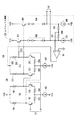
FIG. 1 is a diagram showing a circuit configuration of an
[0045]
In the first embodiment, the
[0046]
105, 106 and 205, 206 are load resistances of the
[0047]
One end sides of the
[0048]
One end sides of the
[0049]
The differential input from the
[0050]
[0051]
The bases of the
[0052]
The
[0053]
[0054]
In this example, the
[0055]
The collector of the
[0056]
For example, when the input voltage of the
[0057]
In the first embodiment, in order to make the
[0058]
Therefore, regarding the common mode voltage of the collector outputs of the
[0059]
The
[0060]
The second
[0061]
The second
[0062]
The base of the
[0063]
In order to make the second
[0064]
Therefore, the base-emitter voltage Vbe of the
[0065]
The other end (cathode side) of the diode group 22 of the second
[0066]
Next, the operation of the first embodiment configured as described above will be described.
[0067]
That is, the level shift of the common mode voltage of the differential output obtained at the collectors of the
[0068]
In this first embodiment, the
[0069]
That is, even if the base-emitter voltage Vbe of the
[0070]
For example, when the input voltage of the
[0071]
The first embodiment is also applied to the case where an input with a large amplitude that saturates the
[0072]
Therefore, according to the first embodiment, even when an excessive input is input with a simple configuration or when the load resistance varies, the waveform as described in the example of FIG. 6 is used. An amplifier circuit with a level shift circuit that does not generate distortion can be provided.
[0073]
According to the first embodiment, the voltage at the cathode side end of the diode group 22 of the second
[0074]
Next, a more specific circuit configuration example of the IC circuit of the amplifier circuit with level shift circuit according to the first embodiment will be described with reference to FIG. In FIG. 2, the same components as those in FIG. 1 are denoted by the same reference numerals.
[0075]
In FIG. 2, 40, 45, 46, 47, 48, 49, 24, 25, 26, and 27 are resistors, and 41, 42, 43, 44, 50, 51, 52, and 53 are NPN transistors. The
[0076]
The
[0077]
Similarly, the
[0078]
First, the operation of the current mirror circuit will be described. Here, for simplicity, the current amplification factor Hfe is infinite.
[0079]
Taking a current mirror circuit composed of
Ic = (Vee−Vbe) / (R40 + R45)
It is expressed.
[0080]
If the sizes of the
[0081]
Further, when the size of the
[0082]
The same applies to the current mirror circuit composed of the
[0083]
In order to improve the uniformity of the current mirror circuit, it is necessary to arrange the
[0084]
Further, in order to reduce the size of the
[0085]
Similarly, the
[0086]
That is, when the
[0087]
Further, similarly, in the first and second
[0088]
That is, when the
[0089]
The above operation affects the
[0090]
As described above, according to the first embodiment, the common mode voltage of the differential output terminal can be set to 0 V with a simple circuit, and when an excessive input or load is applied as in the conventional configuration. An amplifier circuit with a level shift circuit that does not generate waveform distortion caused by variation in resistance can be provided.
[0091]
[Second Embodiment]
In the first embodiment described above, in order to make the
[0092]
However, the present invention is not limited to this, and it is possible to adopt a configuration in which the size of the corresponding NPN transistor, the resistance value of the corresponding load resistor, and the current value of the corresponding current mirror are changed.
[0093]
For example, in the second embodiment, the size of the
[0094]
At the same time, the value of the
[0095]
Further, the size of the
[0096]
According to the second embodiment, since the current value can be reduced, it is possible to reduce the power consumption and the space of the entire circuit, which is very effective as an IC circuit. Further, to save space, the portion of the
[0097]
In the above description of the second embodiment, the current ratio is set to ¼. However, the present invention is not limited to this and can be set to an arbitrary value. In fact, if a very large ratio is selected, the size of the NPN transistor will be reduced, leading to problems such as inaccuracy and the need for high resistance. I need it.
[0098]
[Other embodiments]
In the above description of the embodiment, the common mode voltage of the
[0099]
In the above description, the number of cascade connection stages of the differential amplifier circuit of the
[0100]
In the above description, the transistor has been described as an NPN-type bipolar junction transistor, but the present invention can also be applied to a case of using a field effect transistor (FET).
[0101]
Furthermore, although the
[0102]
【The invention's effect】
As described above, according to the present invention, while maintaining the common mode voltage of the differential output terminal constant, waveform distortion occurs in the differential output even when the amplifier circuit is excessively input or load resistance varies. It is possible to provide an amplifier circuit with a level shift circuit that does not.
[0103]
Therefore, when the amplifier circuit according to the present invention is used in a measuring device such as an oscilloscope, a so-called saturation recovery characteristic (after an excessive waveform that protrudes from the display screen for displaying the waveform is input and the amplifier circuit is saturated) It is possible to provide an oscilloscope with excellent characteristics (whether it can be measured after a lapse of time).
[0104]
In addition, the amplifier circuit with level shift circuit according to the present invention is suitable for IC, and thus has an advantage that it is suitable for miniaturization.
[Brief description of the drawings]
FIG. 1 is a circuit diagram showing a first embodiment of an amplifier circuit with a level shift circuit according to the present invention;
FIG. 2 is a diagram showing a more specific circuit configuration of the first embodiment.
FIG. 3 is a circuit diagram of an example of an amplifier circuit in which a differential amplifier circuit is cascade-connected at an arbitrary number of stages.
FIG. 4 is a circuit diagram of another example of an amplifier circuit in which a differential amplifier circuit is connected in an arbitrary number of stages.
FIG. 5 is a circuit diagram showing an example of a conventional amplifier circuit with a level shift circuit.
FIG. 6 is a circuit diagram showing another example of a conventional amplifier circuit with a level shift circuit.
7 is a diagram obtained by simulating the waveform distortion at the time of excessive input in the case of the conventional example of FIG.
[Explanation of symbols]
150 First amplifier circuit
151 Differential input terminal
152 Differential output terminal
160 Amplifier circuit with level shift circuit
162 Differential output terminal
100,200 differential amplifier circuit
101, 102, 201, 202 NPN transistor
105, 106, 205, 206 Load resistance
107,207 Constant current source
300 First level shift circuit
301,302 NPN transistor
303,304 Diode group
305,306 Constant current source
10 Second amplifier circuit
11 NPN transistor
12 Load resistance
14 Constant current source
15 DC power supply
20 Second level shift circuit
21 NPN transistor
22 Diode group
23 Constant current source
30 operational amplifier
Claims (5)
前記第1の増幅回路の前記差動出力端子に接続され、前記第1の増幅回路の差動出力をレベルシフトして出力するための差動出力端子を備える第1のレベルシフト回路と、
前記第1の増幅回路の前記差動出力端子に最も近い差動増幅回路と等価なものであって、前記第1の増幅回路の前記差動出力端子に最も近い前記差動増幅回路と電源が共通とされる共に、所定の直流電圧が供給される第2の増幅回路と、
前記第2の増幅回路の出力をレベルシフトする、前記第1のレベルシフト回路と等価な第2のレベルシフト回路と、
前記第2のレベルシフト回路の直流出力電圧を一定に保つように、前記差動出力端子に最も近い前記差動増幅回路および前記第2の増幅回路の電源電圧を制御する演算増幅器と
を備えることを特徴とするレベルシフト回路付き増幅回路。A first amplifier circuit having a differential input terminal and a differential output terminal, the differential amplifier circuit being cascade-connected in an arbitrary number of stages;
A first level shift circuit connected to the differential output terminal of the first amplifier circuit and having a differential output terminal for level-shifting and outputting the differential output of the first amplifier circuit;
The differential amplifier circuit closest to the differential output terminal of the first amplifier circuit is equivalent to the differential amplifier circuit closest to the differential output terminal of the first amplifier circuit and a power source A second amplifier circuit which is made common and supplied with a predetermined DC voltage;
A second level shift circuit equivalent to the first level shift circuit for level shifting the output of the second amplifier circuit;
An operational amplifier for controlling the power supply voltage of the second amplifier circuit and the differential amplifier circuit closest to the differential output terminal so as to keep the DC output voltage of the second level shift circuit constant; An amplifier circuit with a level shift circuit characterized by the above.
前記第2の増幅回路は、前記第1の増幅回路の前記差動出力端子に最も近い差動増幅回路の片側の増幅回路と等しい構成とされると共に、前記第2のレベルシフト回路は、前記差動出力をレベルシフトする第1のレベルシフト回路の片側と等しい構成とされる
ことを特徴とするレベルシフト回路付き増幅回路。In claim 1,
The second amplifier circuit is configured to be equal to the amplifier circuit on one side of the differential amplifier circuit closest to the differential output terminal of the first amplifier circuit, and the second level shift circuit includes An amplifier circuit with a level shift circuit, characterized in that it has the same configuration as one side of the first level shift circuit for level shifting the differential output.
前記第1の増幅回路を構成するトランジスタと、前記第2の増幅回路を構成するトランジスタのサイズを等しく構成すると共に、前記第1のレベルシフト回路を構成するトランジスタと、前記第2のレベルシフト回路を構成するトランジスタのサイズを等しく構成した
ことを特徴とするレベルシフト回路付き増幅回路。In claim 3,
The transistor constituting the first amplifier circuit and the transistor constituting the second amplifier circuit are configured to have the same size, the transistor constituting the first level shift circuit, and the second level shift circuit An amplifier circuit with a level shift circuit, characterized in that the sizes of the transistors constituting the circuit are equal.
前記第2の増幅回路を構成するトランジスタのサイズが、前記第1の増幅回路を構成するトランジスタのサイズの1/N(Nは2以上の整数)になるように構成すると共に、前記第2のレベルシフト回路を構成するトランジスタのサイズが、前記第1のレベルシフト回路を構成するトランジスタのサイズの1/N(Nは2以上の整数)になるように構成した
ことを特徴とするレベルシフト回路付き増幅回路。In claim 3,
The transistor constituting the second amplifier circuit is configured so that the size of the transistor constituting the first amplifier circuit is 1 / N (N is an integer of 2 or more), and the second amplifier circuit A level shift circuit characterized in that the size of a transistor constituting the level shift circuit is 1 / N (N is an integer of 2 or more) of the size of the transistor constituting the first level shift circuit. Amplification circuit with.
Priority Applications (1)
| Application Number | Priority Date | Filing Date | Title |
|---|---|---|---|
| JP2001213780A JP3633889B2 (en) | 2000-09-29 | 2001-07-13 | Amplifier circuit with level shift circuit |
Applications Claiming Priority (3)
| Application Number | Priority Date | Filing Date | Title |
|---|---|---|---|
| JP2000-298465 | 2000-09-29 | ||
| JP2000298465 | 2000-09-29 | ||
| JP2001213780A JP3633889B2 (en) | 2000-09-29 | 2001-07-13 | Amplifier circuit with level shift circuit |
Publications (2)
| Publication Number | Publication Date |
|---|---|
| JP2002176322A JP2002176322A (en) | 2002-06-21 |
| JP3633889B2 true JP3633889B2 (en) | 2005-03-30 |
Family
ID=26601088
Family Applications (1)
| Application Number | Title | Priority Date | Filing Date |
|---|---|---|---|
| JP2001213780A Expired - Fee Related JP3633889B2 (en) | 2000-09-29 | 2001-07-13 | Amplifier circuit with level shift circuit |
Country Status (1)
| Country | Link |
|---|---|
| JP (1) | JP3633889B2 (en) |
Families Citing this family (1)
| Publication number | Priority date | Publication date | Assignee | Title |
|---|---|---|---|---|
| JP3833530B2 (en) * | 2001-12-13 | 2006-10-11 | 株式会社東芝 | Differential amplifier |
-
2001
- 2001-07-13 JP JP2001213780A patent/JP3633889B2/en not_active Expired - Fee Related
Also Published As
| Publication number | Publication date |
|---|---|
| JP2002176322A (en) | 2002-06-21 |
Similar Documents
| Publication | Publication Date | Title |
|---|---|---|
| JP3088262B2 (en) | Low distortion differential amplifier circuit | |
| KR0148324B1 (en) | Variable gain amplifying circuit | |
| KR0149650B1 (en) | Current amplifier | |
| US5880639A (en) | Amplification circuit | |
| US20020039049A1 (en) | Amplifying circuit | |
| JP3633889B2 (en) | Amplifier circuit with level shift circuit | |
| JPH1197774A (en) | Output circuit device | |
| US3518458A (en) | Decoupling means for integrated circuit | |
| KR20040045902A (en) | A power amplifier module | |
| JPH06230740A (en) | Signal level conversion circuit | |
| EP1110322B1 (en) | Electronic circuit | |
| US6275076B1 (en) | Sample-and-hold device using complementary bipolar technology | |
| Wilson et al. | Improved logarithmic converter based on a transconductance feedback amplifier | |
| US4491803A (en) | Current-limiting mechanism for a precision differential amplifier | |
| JPH04268810A (en) | Delay circuit | |
| KR930007795B1 (en) | Amp circuit operable at low power amplification | |
| US6400184B1 (en) | Transistor output circuit | |
| JP2004007706A (en) | Variable current dividing circuit | |
| US20080224772A1 (en) | Operational Amplifier Selecting One of Inputs, and an Amplifying Apparatus Using the Op Amplifier the Verification Method | |
| JP3219653B2 (en) | Signal holding circuit | |
| JPH07154168A (en) | Buffer circuit | |
| JPH10341122A (en) | Variable gain amplifier and variable current division circuit | |
| JPH01126816A (en) | Broad band variable gain amplifier circuit | |
| SU1259472A1 (en) | Operational amplifier | |
| JP5350882B2 (en) | Capacity multiplier circuit |
Legal Events
| Date | Code | Title | Description |
|---|---|---|---|
| A977 | Report on retrieval |
Free format text: JAPANESE INTERMEDIATE CODE: A971007 Effective date: 20041130 |
|
| TRDD | Decision of grant or rejection written | ||
| A01 | Written decision to grant a patent or to grant a registration (utility model) |
Free format text: JAPANESE INTERMEDIATE CODE: A01 Effective date: 20041208 |
|
| A61 | First payment of annual fees (during grant procedure) |
Free format text: JAPANESE INTERMEDIATE CODE: A61 Effective date: 20041221 |
|
| R150 | Certificate of patent or registration of utility model |
Free format text: JAPANESE INTERMEDIATE CODE: R150 |
|
| FPAY | Renewal fee payment (event date is renewal date of database) |
Free format text: PAYMENT UNTIL: 20090107 Year of fee payment: 4 |
|
| FPAY | Renewal fee payment (event date is renewal date of database) |
Free format text: PAYMENT UNTIL: 20100107 Year of fee payment: 5 |
|
| FPAY | Renewal fee payment (event date is renewal date of database) |
Free format text: PAYMENT UNTIL: 20110107 Year of fee payment: 6 |
|
| FPAY | Renewal fee payment (event date is renewal date of database) |
Free format text: PAYMENT UNTIL: 20120107 Year of fee payment: 7 |
|
| FPAY | Renewal fee payment (event date is renewal date of database) |
Free format text: PAYMENT UNTIL: 20130107 Year of fee payment: 8 |
|
| FPAY | Renewal fee payment (event date is renewal date of database) |
Free format text: PAYMENT UNTIL: 20140107 Year of fee payment: 9 |
|
| LAPS | Cancellation because of no payment of annual fees |