JP3631471B2 - Liquid crystal display controller - Google Patents
Liquid crystal display controller Download PDFInfo
- Publication number
- JP3631471B2 JP3631471B2 JP2002106918A JP2002106918A JP3631471B2 JP 3631471 B2 JP3631471 B2 JP 3631471B2 JP 2002106918 A JP2002106918 A JP 2002106918A JP 2002106918 A JP2002106918 A JP 2002106918A JP 3631471 B2 JP3631471 B2 JP 3631471B2
- Authority
- JP
- Japan
- Prior art keywords
- pixels
- basic
- liquid crystal
- crystal display
- gradation
- Prior art date
- Legal status (The legal status is an assumption and is not a legal conclusion. Google has not performed a legal analysis and makes no representation as to the accuracy of the status listed.)
- Expired - Fee Related
Links
Images


Classifications
-
- G—PHYSICS
- G09—EDUCATION; CRYPTOGRAPHY; DISPLAY; ADVERTISING; SEALS
- G09G—ARRANGEMENTS OR CIRCUITS FOR CONTROL OF INDICATING DEVICES USING STATIC MEANS TO PRESENT VARIABLE INFORMATION
- G09G3/00—Control arrangements or circuits, of interest only in connection with visual indicators other than cathode-ray tubes
- G09G3/20—Control arrangements or circuits, of interest only in connection with visual indicators other than cathode-ray tubes for presentation of an assembly of a number of characters, e.g. a page, by composing the assembly by combination of individual elements arranged in a matrix no fixed position being assigned to or needed to be assigned to the individual characters or partial characters
- G09G3/34—Control arrangements or circuits, of interest only in connection with visual indicators other than cathode-ray tubes for presentation of an assembly of a number of characters, e.g. a page, by composing the assembly by combination of individual elements arranged in a matrix no fixed position being assigned to or needed to be assigned to the individual characters or partial characters by control of light from an independent source
- G09G3/36—Control arrangements or circuits, of interest only in connection with visual indicators other than cathode-ray tubes for presentation of an assembly of a number of characters, e.g. a page, by composing the assembly by combination of individual elements arranged in a matrix no fixed position being assigned to or needed to be assigned to the individual characters or partial characters by control of light from an independent source using liquid crystals
- G09G3/3611—Control of matrices with row and column drivers
-
- G—PHYSICS
- G09—EDUCATION; CRYPTOGRAPHY; DISPLAY; ADVERTISING; SEALS
- G09G—ARRANGEMENTS OR CIRCUITS FOR CONTROL OF INDICATING DEVICES USING STATIC MEANS TO PRESENT VARIABLE INFORMATION
- G09G3/00—Control arrangements or circuits, of interest only in connection with visual indicators other than cathode-ray tubes
- G09G3/20—Control arrangements or circuits, of interest only in connection with visual indicators other than cathode-ray tubes for presentation of an assembly of a number of characters, e.g. a page, by composing the assembly by combination of individual elements arranged in a matrix no fixed position being assigned to or needed to be assigned to the individual characters or partial characters
- G09G3/2007—Display of intermediate tones
- G09G3/2018—Display of intermediate tones by time modulation using two or more time intervals
- G09G3/2022—Display of intermediate tones by time modulation using two or more time intervals using sub-frames
-
- G—PHYSICS
- G09—EDUCATION; CRYPTOGRAPHY; DISPLAY; ADVERTISING; SEALS
- G09G—ARRANGEMENTS OR CIRCUITS FOR CONTROL OF INDICATING DEVICES USING STATIC MEANS TO PRESENT VARIABLE INFORMATION
- G09G3/00—Control arrangements or circuits, of interest only in connection with visual indicators other than cathode-ray tubes
- G09G3/20—Control arrangements or circuits, of interest only in connection with visual indicators other than cathode-ray tubes for presentation of an assembly of a number of characters, e.g. a page, by composing the assembly by combination of individual elements arranged in a matrix no fixed position being assigned to or needed to be assigned to the individual characters or partial characters
- G09G3/2007—Display of intermediate tones
- G09G3/2044—Display of intermediate tones using dithering
- G09G3/2051—Display of intermediate tones using dithering with use of a spatial dither pattern
- G09G3/2055—Display of intermediate tones using dithering with use of a spatial dither pattern the pattern being varied in time
Landscapes
- Engineering & Computer Science (AREA)
- Chemical & Material Sciences (AREA)
- Crystallography & Structural Chemistry (AREA)
- Physics & Mathematics (AREA)
- Computer Hardware Design (AREA)
- General Physics & Mathematics (AREA)
- Theoretical Computer Science (AREA)
- Control Of Indicators Other Than Cathode Ray Tubes (AREA)
- Liquid Crystal Display Device Control (AREA)
- Liquid Crystal (AREA)
Description
【0001】
【発明の属する技術分野】
本発明は、液晶表示制御装置に関する。
【0002】
【従来の技術】
単独画素では2値表示(オン状態の表示とオフ状態の表示)しかできないマトリクス型の液晶表示パネル(LCDパネル)において階調表示を行う方法として、フレーム変調方式の階調表示方法が知られている。このフレーム変調方式では、時間軸方向でオン表示とオフ表示を組み合わせることで、擬似的に階調表示を可能としている。例えば、16階調の画像を表示する場合には、16フレームを1周期とし、階調レベルに応じてオン状態及びオフ状態のフレームを規定することで、16フレームの平均値として所望の階調が得られる。
【0003】
このように、フレーム変調方式では、複数のフレームを1周期として表示を行うため、階調レベル数が増加すると、フリッカー等が目立ちやすくなり、表示品質が悪化する。そのため、例えば16階調の画像を表示する場合には、水平方向4画素、垂直方向4画素の合計4×4=16画素を用いて表示パターンを作成し、表示品質の悪化を抑制するようにしている。
【0004】
ここで、上述したような表示パターンを記憶するために必要な記憶容量について考える。16階調の画像を表示する場合には、各階調レベル毎に16画素で構成された表示パターンを16フレーム分用いる必要がある。したがって、16(表示パターンの画素数)×16(フレーム数)×16(階調レベル数)=4096ビット分の記憶容量が必要となる。メモリを内蔵したマイクロコンピュータによって表示制御を行う場合、内蔵されるメモリの容量が少ないため、表示パターンを記憶するための容量をできるだけ少なくすることが好ましい。
【0005】
また、フレーム変調方式では、各階調レベルにおける表示パターンについて必ずしも最適化されているとは言えず、そのために表示品質が悪化するという問題もあった。
【0006】
【発明が解決しようとする課題】
このように、従来は、表示パターンを記憶するための容量が多くなるといった問題があった。
【0007】
本発明は、上記従来の課題に対してなされたものであり、表示パターンを記憶するための容量を低減することが可能な液晶表示制御装置を提供することを目的としている。
【0008】
【課題を解決するための手段】
本発明に係る液晶表示制御装置は、オン状態の画素とオフ状態の画素を複数のフレーム及び複数の画素に分散させることで、液晶表示パネル上に総階調レベル数がNの画像を表示するように構成された液晶表示制御装置であって、複数の基本画素それぞれにオン状態及びオフ状態の一方を設定した2値表示パターンを、複数の基本フレームそれぞれについて設定することで得られたパターン情報を、階調レベル毎に記憶した記憶部と、前記記憶部に記憶されたパターン情報のなかから、指定された階調レベルに対応したパターン情報を選択する選択部と、を備え、前記基本フレームの数及び前記基本画素の数は対応する階調レベルに応じて決められており、各階調レベルについて前記基本フレームの数と前記基本画素の数は等しいことを特徴とする。
【0010】
【発明の実施の形態】
以下、本発明の実施形態を図面を参照して説明する。
【0011】
(実施形態1)
以下、単独画素では2値表示しかできないマトリクス型の液晶表示パネルに、16階調の画像を表示する場合を想定して説明する。なお、16階調の画像を表示する場合、すべての画素がオフ状態である場合(第0階調レベル)からすべての画素がオン状態である場合(第16階調レベル)まで合計17の階調レベルが存在し得るが、第15階調レベル(15の画素がオン状態である場合)は用いず、階調レベルの合計数が16になるようにしている。
【0012】
図1は、本実施形態に係る液晶表示制御装置の構成例を示したブロック図である。本液晶表示制御装置は、制御部11、各階調レベルの2値表示パターン(以下、単に表示パターンと言う場合もある)が記憶された記憶部(ルックアップテーブル)12、指示された階調レベルに応じたパターン情報(表示パターンの集合)を選択する選択部13によって構成されており、これらの構成要素は単一のICチップに内蔵されている。
【0013】
本実施形態では、表示パターンを構成するための画素(基本画素)の数を階調レベルに応じて変えている。また、表示パターンの数(基本フレームの数)も階調レベルに応じて変えている。例えば、基本画素数が4の場合、基本フレームの繰り返し周期も4となるため、基本フレーム数も4となる。具体的には、図2に示すように、第1、第3、第5、第7、第9、第11及び第13階調レベル(以下、第1タイプという)については(図2(a)参照)、4×4=16画素で基本画素群を構成し、基本フレームの数を16としている。また、第2、第6、第10及び第14階調レベル(以下、第2タイプという)については(図2(b)参照)、4×2=8画素で基本画素群を構成し、基本フレームの数を8としている。また、第4及び第12階調レベル(以下、第3タイプという)については(図2(c)参照)、2×2=4画素で基本画素群を構成し、基本フレームの数を4としている。さらに、第8階調レベル(以下、第4タイプという)については(図2(d)参照)、2×1=2画素で基本画素群を構成し、基本フレームの数を2としている。なお、図2において、各画素内に示した(i,j)は、基本画素群におけるX方向及びY方向の画素位置である。
【0014】
図3は、上述した第1〜第4タイプにおける各基本画素群の配置を示したものである。図3(a)は第1タイプについて、図3(b)は第2タイプについて、図3(c)は第3タイプについて、図3(d)は第4タイプについて、それぞれ示している。
【0015】
図4は、一例として、第7階調レベルについて設定される各基本フレームの表示パターンを示したものである。図4に示すように、各基本フレームいずれも7個の画素がオン状態となっている。また、基本画素群に含まれるいずれの画素も、16フレームのうち7フレームでオン状態となっている。
【0016】
ここで、上述したような手法を採用した場合の総記憶容量について考える。第1タイプについては、16(表示パターンの画素数)×16(フレーム数)×7(階調レベル数)=1792ビット分の記憶容量となる。第2タイプについては、8(表示パターンの画素数)×8(フレーム数)×4(階調レベル数)=256ビット分の記憶容量となる。第3タイプについては、4(表示パターンの画素数)×4(フレーム数)×2(階調レベル数)=32ビット分の記憶容量となる。第4タイプについては、2(表示パターンの画素数)×2(フレーム数)×1(階調レベル数)=4ビット分の記憶容量となる。したがって、記憶容量の合計は、1792+256+32+4=2084ビットとなり、従来の記憶容量(4096ビット)の半分近くに低減される。
【0017】
また、第8階調レベルを中心にして、(8−c)で表される階調レベルと(8+c)で表される階調レベルとの間では、パターン情報を共通化することが可能である。すなわち、第(8−c)階調レベルの各表示パターンは、第(8+c)階調レベルの対応する表示パターンを反転させる(オン表示画素をオフ表示画素に、オフ表示画素をオン表示画素にする)ことで得ることが可能である。したがって、パターン情報を共通化することで、記憶容量をさらに低減することも可能である。具体的には、第1タイプについては、第7と第9階調レベル、第5と第11階調レベル、第3と第13階調レベルをそれぞれ共通化することで、1024ビット分の記憶容量となる。また、第2タイプについては、第6と第10階調レベル、第2と第14階調レベルをそれぞれ共通化することで、128ビット分の記憶容量となる。第3タイプについては、第4と第12階調レベルを共通化することで、16ビット分の記憶容量となる。したがって、記憶容量の合計は、1024+128+16+4=1172ビットとなり、記憶容量が大幅に低減される。
【0018】
図5は、本実施形態に係る液晶表示制御装置の具体的な構成及び動作を説明するための図である。
【0019】
21a〜21dは表示パターンを記憶する記憶部(ルックアップテーブル)に対応するものであり、21aは第1、第3、第5、第7、第9、第11及び第13階調レベル(第1タイプ)の表示パターンを記憶する部分、21bは第2、第6、第10及び第14階調レベル(第2タイプ)を記憶する部分、21cは第4及び第12階調レベル(第3タイプ)を記憶する部分、第8階調レベル(第4タイプ)を記憶する部分である。22は選択部に対応し、記憶部21a〜21dからの表示パターンを選択するものである。23a〜23cは演算部、24はカウンタである。
【0020】
4ビットのカウンタ24には、フレームパルスが入力され、4ビットのカウント値k[3:0]が出力される。
【0021】
演算部23aには4ビットのカウント値k[3:0]及び現画素のY座標値の下位2ビットを表すデータj[1:0]が入力し、演算部23aでの演算結果(4×k+j)はアドレスデータとして記憶部21aに出力される。記憶部21aからは、指定されたアドレスに記憶されている4ビットデータが出力される。
【0022】
演算部23bにはカウント値の下位3ビットk[2:0]及びY座標値の下位1ビットj[0]が入力し、演算部23bでの演算結果(2×k[2:0]+j[0])はアドレスデータとして記憶部21bに出力される。記憶部21bからは、指定されたアドレスに記憶されている4ビットデータが出力される。
【0023】
演算部23cにはカウント値の下位2ビットk[1:0]及びY座標値の下位1ビットj[0]が入力し、演算部23cでの演算結果(2×k[1:0]+j[0])はアドレスデータとして記憶部21cに出力される。記憶部21cからは、指定されたアドレスに記憶されている2ビットデータが4ビットデータに変換されて出力される。
【0024】
記憶部21dには、アドレスデータとしてカウント値の下位1ビットk[0]が入力し、記憶部21dからは、指定されたアドレスに記憶されている2ビットデータが4ビットデータに変換されて出力される。
【0025】
上述した動作により、選択部22には記憶部21a〜21dに記憶されている各階調レベルLのデータが入力する。図5では、例えば第1タイプの第1階調レベルのデータはT1(for L=1)、第2タイプの第2階調レベルのデータはT2(for L=2)として示している。
【0026】
また、選択部22には、外部から3原色(R、G、B)の各階調レベルを表す4ビットデータ(Rの階調レベルL(R)、Gの階調レベルL(G)、Bの階調レベルL(B))が入力するとともに、現画素のX座標値の下位2ビットi[1:0]が入力する。これらのデータに基づき、選択部22からは、各原色の1ビットの出力データ(Rout、Gout、Bout)が順次出力される。すなわち、階調レベルが第1タイプ〜第4タイプに属する場合(第1〜第14階調の場合)には、記憶部21a〜21dからのデータのいずれか一つが選択され、X座標値の下位2ビットi[1:0]に応じて、選択されたデータが順次出力される。また、階調レベルが第0階調の場合にはオフ表示状態のデータ(論理値0)が、階調レベルが第16階調の場合にはオン表示状態のデータ(論理値1)が、それぞれ出力されることになる。
【0027】
以上のように、本実施形態によれば、階調レベルに応じて基本フレームの数及び基本画素の数を設定しているので、表示パターンを記憶するための容量を大幅に削減することができる。したがって、特にメモリを内蔵したマイクロコンピュータによって液晶表示パネルの表示制御を行う場合等、メモリ容量が少ない場合に効果的である。
【0028】
なお、上述した実施形態では、総階調レベル数Nが16(N=16)の画像を表示する場合を想定して説明したが、総階調レベル数Nは限定されるものではない。特に、(N/a)×b(ただし、a及びN/aは2以上の整数、bは0より大きくaより小さい整数)で表される階調レベルが存在する場合には、そのような階調レベルについては基本フレーム及び基本画素の数を共にaにできるため、記憶容量を効果的に低減することができる。また、総階調レベル数Nがn2 (ただし、nは2以上の整数)で表される場合、基本画素群の構成をn×n(X方向n画素、Y方向n画素)にできるため、表示品質の劣化が少ない階調表示が得られる。ただし、n2 が奇数の場合には、総階調レベル数Nは、N=n2 +1(ただし、n2 が奇数の場合)であることが好ましい。さらに、パターン情報を共通化する場合には、一般に、cを0より大きく<N/2より小さい整数として、cで表される階調レベルとN−cで表される階調レベルとで、パターン情報を共通化することが好ましい。
【0029】
(実施形態2)
次に、各階調レベルにおいて最適な表示パターンを得るための方法について説明する。なお、第1の実施形態で説明した事項と重複する事項については、説明は省略する。
【0030】
図6は、第1、第3、第5、第7、第9、第11及び第13階調レベル(第1タイプ)について、基本画素群を配列した状態を示したものである。ある画素(中心画素、例えば図6の円内の画素(0,0))の輝度を考えると、中心画素の輝度は、中心画素自身の輝度の他に、さらに周囲の画素の輝度の影響が付加されたものとなる。画素(i,j)において、画素(i,j)自身の輝度をg1[j][i]とし、周囲の画素の輝度の影響を付加した画素(i,j)の実際の輝度をg2[j][i]とすると、g2[j][i]は以下のように表すことができる。
【0031】

Kc(r2/r1)=(r2/r1)r (1.5≦r≦2.5)
である。
【0032】
r1は点灯画素が球体であると仮定した場合の半径、r2は点灯画素からの距離であり、rの値は理論的には2となる。また、C(i)は、”i mod 4” を意味するものであり、例えば C(1) = C(5) = C(−3) となる。また、”sqrt”は、スクエアルートを意味する。
【0033】
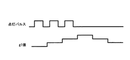
また、ある画素のあるフレームでの輝度は、その前のフレームの影響も受ける。例えば、図7に示すように、ある画素が連続的に点灯すると、ある画素の輝度はしだいに上昇する。そこで、ある画素のあるフレームでの輝度をg1(j,i)とし、次のフレームでの輝度をg1(j,i)nextとすると、
g1(j,i)next = g1(j,i)*(1−Kr)+Kr*Ps(j,i) (式2)
と表すことができる。ただし、0.05≦Kr≦0.2であり、一般的には、Kr=0.1 である。また、Ps(j,i)は、画素が点灯している場合には1、点灯していない場合には0となる。
【0034】
以下、上述した事項を考慮して、最適な表示パターンを得るための具体的な方法を、図8に示したフローチャートを参照して説明する。なお、ここでは、図4に示すような第7階調レベルの表示パターンを求める場合を例に説明する。
【0035】
ステップS1では、初期設定を行う。すなわち、基本フレーム数=16、基本画素群の画素数=16、基本画素群における点灯画素数=7を設定する。さらに、第1フレームの基本画素群において最初に点灯する画素を仮に設定する。ここでは、g1(0,0)=1 (点灯状態)、他の画素について g1(j,i)=0 (非点灯状態)とする。
【0036】
ステップS2では、現在選択されている基本フレームの基本画素群のなかで、その時点における最も暗い画素を点灯画素として求める。まず、式1に基づき、現在の基本画素群に含まれる16個全ての基本画素について、g2(j,i) (ただし、0≦i≦3、0≦j≦3)の値を計算によって求める。続いて、それらのなかで最も暗い画素を(Jmin, Imin)として決定する。
【0037】
ステップS3では、ステップS2で求められた画素(Jmin, Imin)を点灯した状態を設定する。そして、式2に基づき、
g1(Jmin, Imin)next = g1(Jmin, Imin)+Kr*Ps(Jmin, Imin)
を設定する。
【0038】
ステップS4では、ステップS2及びS3が所定回数(7回)実行されたか否かが判断される。すなわち、現在選択されている基本画素群について、7個の点灯画素が全て求められたか否かが判断される。点灯画素の全てについてはまだ求められていないと判断された場合には、ステップ2に戻って、次に点灯すべき画素を求める。7個の点灯画素が全て求められていると判断された場合には、ステップS5において、求められた7個の点灯画素のパターンを仮の表示パターンとして決定する。
【0039】
ステップS6では、次の基本フレームの設定を行う。すなわち、式2に基づいて、
g1(j,i)next = g1(j,i)*(1−Kr)
の値を基本画素群に含まれる16個全ての基本画素について求める。
【0040】
ステップS7では、すべての基本フレーム(16個のフレーム)について、求められた仮の表示パターンが安定であるか否かが判断される。具体的には、各基本フレームについて、最後に決定された表示パターンとその前(16フレーム前)に決定された表示パターンとを比較し、それらの誤差が一定値以下である場合には、16フレーム全てについて表示パターン(仮の表示パターン)が安定であると見なす。ステップS7において、表示パターンが安定でないと判断された場合には、ステップ2に戻り、次のフレームについて動作を実行する。
【0041】
ステップS7において、表示パターンが安定であると判断された場合には、ステップ8において、求められた16フレーム分の仮の表示パターンを最終的な表示パターンとして決定する。決定された最終的な表示パターンは、液晶表示制御装置内の記憶部に記憶される。
【0042】
上述した動作を図4を参照して説明すると、まず第0フレーム〜第15フレームそれぞれについて、表示パターン(7画素が点灯状態の表示パターン)が仮に決定される。その後、次の第0フレーム〜第15フレームについて同様の動作が行われる。すなわち、それまでに仮に決定された各表示パターンの影響を考慮して、第0フレーム〜第15フレームの各表示パターンが順次更新され、更新された表示パターンが仮の表示パターンとして順次決定される。したがって、各フレームにおいて仮の表示パターンが決定された段階では、第0フレーム〜第15フレーム全てについて、7画素が点灯状態の表示パターンが得られている。したがって、各フレームにおいて仮の表示パターンが決定された段階毎に、ステップS7の判断が行われることになる。
【0043】
以上のように、本実施形態によれば、その時点における最も暗い画素を求めて点灯するとういう原則に基づいて、最適な表示パターンを決定するようにしている。オン状態の画素(点灯画素)とオフ状態の画素(非点灯画素)を時間的及び空間的に分散させて階調表示を行う場合、点灯画素ができるだけ分散されている方が、人間の眼の特性上、良好な画像が認識される。本実施形態の手法を用いることで、点灯画素を時間的及び空間的に効果的に分散させることができ、最適化された表示パターンを得ることができる。また、各フレームの表示パターンが安定するまで繰り返し動作が実行されるので、極めて精度よく表示パターンを決定することができる。
【0044】
なお、上述した実施形態では、総階調レベル数Nが16の場合について、第7階調レベルの表示パターンを求める例について説明したが、その他の階調レベルについても同様の手法を適用することができる。また、総階調レベル数Nは16に限らず、例えば第1の実施形態で記載したような総階調レベル数についても、本実施形態の手法は同様に適用可能である。
【0045】
以上、本発明の実施形態を説明したが、本発明は上記実施形態に限定されるものではなく、その趣旨を逸脱しない範囲内において種々変形して実施することが可能である。さらに、上記実施形態には種々の段階の発明が含まれており、開示された構成要件を適宜組み合わせることによって種々の発明が抽出され得る。例えば、開示された構成要件からいくつかの構成要件が削除されても、所定の効果が得られるものであれば発明として抽出され得る。
【0046】
【発明の効果】
本発明によれば、表示パターンを記憶するための容量を低減することが可能となる。したがって、優れた液晶表示制御装置を提供することが可能となる。
【図面の簡単な説明】
【図1】本発明の実施形態に係る液晶表示制御装置の構成例を示したブロック図。
【図2】本発明の実施形態に係り、基本画素群の一例を示した図。
【図3】本発明の実施形態に係り、基本画素群の配列状態の一例を示した図。
【図4】本発明の実施形態に係り、表示パターンの一例を示した図。
【図5】本実施形態に係る液晶表示制御装置の具体的な構成及び動作を説明するための図。
【図6】本発明の実施形態に係り、基本画素群の配列状態の一例を示した図。
【図7】本発明の実施形態に係り、画素の輝度の変化の一例を示した図。
【図8】本発明の実施形態に係り、最適な表示パターンを得るための方法の一例を示したフローチャート。
【符号の説明】
11…制御部
12、21a、21b、21c、21d…記憶部
13、22…選択部
23a、23b、23c…演算部
24…カウンタ[0001]
BACKGROUND OF THE INVENTION
The present invention relates to a liquid crystal display control device.
[0002]
[Prior art]
As a method for performing gradation display in a matrix type liquid crystal display panel (LCD panel) that can only perform binary display (display in an on state and display in an off state) with a single pixel, a gradation display method using a frame modulation method is known. Yes. In this frame modulation method, pseudo gradation display is possible by combining ON display and OFF display in the time axis direction. For example, in the case of displaying an image with 16 gradations, 16 frames is defined as one cycle, and an on-state frame and an off-state frame are defined according to the gradation level. Is obtained.
[0003]
As described above, in the frame modulation method, display is performed with a plurality of frames as one cycle. Therefore, when the number of gradation levels increases, flicker or the like becomes more conspicuous and display quality deteriorates. Therefore, for example, when displaying an image of 16 gradations, a display pattern is created using a total of 4 × 4 = 16 pixels of 4 pixels in the horizontal direction and 4 pixels in the vertical direction to suppress deterioration in display quality. ing.
[0004]
Here, the storage capacity necessary for storing the display pattern as described above will be considered. When displaying an image of 16 gradations, it is necessary to use a display pattern composed of 16 pixels for each gradation level for 16 frames. Accordingly, a storage capacity of 16 (number of pixels of the display pattern) × 16 (number of frames) × 16 (number of gradation levels) = 4096 bits is required. When display control is performed by a microcomputer having a built-in memory, since the capacity of the built-in memory is small, it is preferable to reduce the capacity for storing the display pattern as much as possible.
[0005]
Further, in the frame modulation method, it cannot be said that the display pattern at each gradation level is necessarily optimized, and there is a problem that display quality deteriorates.
[0006]
[Problems to be solved by the invention]
As described above, conventionally, there is a problem that the capacity for storing the display pattern increases .
[0007]
The present invention has been made to solve the above-described conventional problems, and an object thereof is to provide a liquid crystal display control device capable of reducing the capacity for storing a display pattern .
[0008]
[Means for Solving the Problems]
The liquid crystal display control device according to the present invention displays an image having a total number of gradation levels of N on the liquid crystal display panel by dispersing the on-state pixels and the off-state pixels into a plurality of frames and a plurality of pixels. Pattern information obtained by setting a binary display pattern in which one of an ON state and an OFF state is set for each of a plurality of basic pixels for each of the plurality of basic frames. For each gradation level, and a selection unit for selecting pattern information corresponding to a designated gradation level from among the pattern information stored in the storage unit, and the basic frame wherein the number and the number of the basic pixel has been determined according to the corresponding gray level, the number of the basic pixel and the number of the basic frame equal for each tone level To.
[0010]
DETAILED DESCRIPTION OF THE INVENTION
Hereinafter, embodiments of the present invention will be described with reference to the drawings.
[0011]
(Embodiment 1)
In the following description, it is assumed that a 16-gradation image is displayed on a matrix type liquid crystal display panel that can only perform binary display with a single pixel. When displaying a 16-gradation image, a total of 17 floors from when all the pixels are in the off state (0th gradation level) to when all the pixels are in the on state (16th gradation level) are displayed. There are tone levels, but the 15th tone level (when 15 pixels are in the on state) is not used, and the total number of tone levels is set to 16.
[0012]
FIG. 1 is a block diagram illustrating a configuration example of a liquid crystal display control device according to the present embodiment. The present liquid crystal display control apparatus includes a
[0013]
In the present embodiment, the number of pixels (basic pixels) for configuring the display pattern is changed according to the gradation level. The number of display patterns (number of basic frames) is also changed according to the gradation level. For example, when the number of basic pixels is 4, the basic frame repetition period is also 4, and thus the number of basic frames is also 4. Specifically, as shown in FIG. 2, the first, third, fifth, seventh, ninth, eleventh and thirteenth gradation levels (hereinafter referred to as the first type) are shown in FIG. )) A basic pixel group is composed of 4 × 4 = 16 pixels, and the number of basic frames is 16. For the second, sixth, tenth and fourteenth gradation levels (hereinafter referred to as the second type) (see FIG. 2B), a basic pixel group is formed by 4 × 2 = 8 pixels, and the basic The number of frames is 8. For the fourth and twelfth gradation levels (hereinafter referred to as the third type) (see FIG. 2 (c)), a basic pixel group is composed of 2 × 2 = 4 pixels, and the number of basic frames is four. Yes. Further, for the eighth gradation level (hereinafter referred to as the fourth type) (see FIG. 2D), a basic pixel group is composed of 2 × 1 = 2 pixels, and the number of basic frames is two. In FIG. 2, (i, j) shown in each pixel is a pixel position in the X direction and the Y direction in the basic pixel group.
[0014]
FIG. 3 shows the arrangement of the basic pixel groups in the first to fourth types described above. 3A shows the first type, FIG. 3B shows the second type, FIG. 3C shows the third type, and FIG. 3D shows the fourth type.
[0015]
FIG. 4 shows, as an example, a display pattern of each basic frame set for the seventh gradation level. As shown in FIG. 4, in each basic frame, seven pixels are turned on. In addition, all the pixels included in the basic pixel group are turned on in 7 frames out of 16 frames.
[0016]
Here, the total storage capacity when the above-described method is adopted will be considered. For the first type, 16 (the number of pixels in the display pattern) × 16 (the number of frames) × 7 (the number of gradation levels) = 1792 bits of storage capacity. For the second type, 8 (the number of pixels in the display pattern) × 8 (the number of frames) × 4 (the number of gradation levels) = the storage capacity for 256 bits. For the third type, 4 (the number of pixels in the display pattern) × 4 (the number of frames) × 2 (the number of gradation levels) = 32 bits of storage capacity. For the fourth type, 2 (the number of pixels in the display pattern) × 2 (the number of frames) × 1 (the number of gradation levels) = 4 bits of storage capacity. Therefore, the total storage capacity is 1792 + 256 + 32 + 4 = 2084 bits, which is reduced to almost half of the conventional storage capacity (4096 bits).
[0017]
Further, with the eighth gradation level as the center, pattern information can be shared between the gradation level represented by (8-c) and the gradation level represented by (8 + c). is there. That is, each display pattern of the (8-c) gradation level inverts the display pattern corresponding to the (8 + c) gradation level (an on display pixel is an off display pixel and an off display pixel is an on display pixel). It is possible to obtain it. Therefore, it is possible to further reduce the storage capacity by sharing the pattern information. Specifically, for the first type, the seventh and ninth gradation levels, the fifth and eleventh gradation levels, and the third and thirteenth gradation levels are shared, thereby storing 1024 bits. It becomes capacity. For the second type, the sixth and tenth gradation levels and the second and fourteenth gradation levels are made common to provide a storage capacity of 128 bits. For the third type, by sharing the fourth and twelfth gradation levels, a storage capacity of 16 bits is obtained. Therefore, the total storage capacity is 1024 + 128 + 16 + 4 = 1172 bits, and the storage capacity is greatly reduced.
[0018]
FIG. 5 is a diagram for explaining a specific configuration and operation of the liquid crystal display control device according to the present embodiment.
[0019]
[0020]
The 4-
[0021]
A 4-bit count value k [3: 0] and data j [1: 0] representing the lower 2 bits of the Y coordinate value of the current pixel are input to the
[0022]
The
[0023]
The
[0024]
The storage unit 21d receives the lower 1 bit k [0] of the count value as address data, and the storage unit 21d converts the 2-bit data stored at the designated address into 4-bit data and outputs it. Is done.
[0025]
Through the above-described operation, the data of each gradation level L stored in the
[0026]
Further, the
[0027]
As described above, according to the present embodiment, since the number of basic frames and the number of basic pixels are set according to the gradation level, the capacity for storing the display pattern can be greatly reduced. . Therefore, this is particularly effective when the memory capacity is small, such as when the display control of the liquid crystal display panel is performed by a microcomputer incorporating a memory.
[0028]
In the above-described embodiment, the case where an image having a total gradation level number N of 16 (N = 16) is displayed has been described. However, the total gradation level number N is not limited. In particular, when there is a gradation level represented by (N / a) × b (where a and N / a are integers of 2 or more, b is an integer greater than 0 and less than a), such a level is present. Regarding the gradation level, since the number of basic frames and basic pixels can be both a, the storage capacity can be effectively reduced. Further, when the total number of gradation levels N is represented by n 2 (where n is an integer of 2 or more), the basic pixel group configuration can be n × n (n pixels in the X direction and n pixels in the Y direction). Thus, a gradation display with little deterioration in display quality can be obtained. However, when n 2 is an odd number, the total number of gradation levels N is preferably N = n 2 +1 (where n 2 is an odd number). Further, when pattern information is shared, generally, c is an integer greater than 0 and smaller than N / 2, and the gradation level represented by c and the gradation level represented by Nc are: It is preferable to share pattern information.
[0029]
(Embodiment 2)
Next, a method for obtaining an optimal display pattern at each gradation level will be described. In addition, about the matter which overlaps with the matter demonstrated in 1st Embodiment, description is abbreviate | omitted.
[0030]
FIG. 6 shows a state in which basic pixel groups are arranged for the first, third, fifth, seventh, ninth, eleventh and thirteenth gradation levels (first type). Considering the brightness of a certain pixel (center pixel, for example, pixel (0, 0) in the circle in FIG. 6), the brightness of the center pixel is influenced by the brightness of surrounding pixels in addition to the brightness of the center pixel itself. It will be added. In the pixel (i, j), the luminance of the pixel (i, j) itself is g1 [j] [i], and the actual luminance of the pixel (i, j) to which the influence of the luminance of surrounding pixels is added is g2 [j]. If j] [i], then g2 [j] [i] can be expressed as follows:
[0031]
Kc (r2 / r1) = (r2 / r1) r (1.5 ≦ r ≦ 2.5)
It is.
[0032]
r1 is a radius when the lit pixel is assumed to be a sphere, r2 is a distance from the lit pixel, and the value of r is theoretically 2. C (i) means “i
[0033]
In addition, the luminance of a certain pixel in a certain frame is also affected by the previous frame. For example, as shown in FIG. 7, when a certain pixel is lit continuously, the luminance of the certain pixel gradually increases. Therefore, if the luminance of a certain pixel in a certain frame is g1 (j, i) and the luminance in the next frame is g1 (j, i) next,
g1 (j, i) next = g1 (j, i) * (1-Kr) + Kr * Ps (j, i) (Formula 2)
It can be expressed as. However, 0.05 ≦ Kr ≦ 0.2, and in general, Kr = 0.1. Ps (j, i) is 1 when the pixel is lit and 0 when the pixel is not lit.
[0034]
Hereinafter, a specific method for obtaining an optimal display pattern in consideration of the above-described matters will be described with reference to the flowchart shown in FIG. Here, a case where a display pattern of the seventh gradation level as shown in FIG. 4 is obtained will be described as an example.
[0035]
In step S1, initialization is performed. That is, the number of basic frames = 16, the number of pixels in the basic pixel group = 16, and the number of lighting pixels in the basic pixel group = 7 are set. Further, the first pixel to be lit in the basic pixel group of the first frame is temporarily set. Here, g1 (0,0) = 1 (lighting state) and g1 (j, i) = 0 (non-lighting state) for other pixels.
[0036]
In step S2, the darkest pixel at that point in the basic pixel group of the currently selected basic frame is obtained as the lighting pixel. First, based on
[0037]
In step S3, a state in which the pixel (Jmin, Imin) obtained in step S2 is turned on is set. And based on
g1 (Jmin, Imin) next = g1 (Jmin, Imin) + Kr * Ps (Jmin, Imin)
Set.
[0038]
In step S4, it is determined whether or not steps S2 and S3 have been executed a predetermined number of times (seven times). That is, it is determined whether or not all seven lighting pixels have been obtained for the currently selected basic pixel group. If it is determined that all the lit pixels have not yet been obtained, the process returns to step 2 to obtain the next pixel to be lit. If it is determined that all seven lighting pixels have been obtained, in step S5, the obtained pattern of the seven lighting pixels is determined as a temporary display pattern.
[0039]
In step S6, the next basic frame is set. That is, based on
g1 (j, i) next = g1 (j, i) * (1-Kr)
For all 16 basic pixels included in the basic pixel group.
[0040]
In step S7, it is determined whether or not the obtained temporary display pattern is stable for all basic frames (16 frames). Specifically, for each basic frame, the last determined display pattern is compared with the display pattern determined before (16 frames before), and when the error is equal to or less than a certain value, The display pattern (provisional display pattern) is assumed to be stable for all frames. If it is determined in step S7 that the display pattern is not stable, the process returns to step 2 to execute the operation for the next frame.
[0041]
If it is determined in step S7 that the display pattern is stable, in
[0042]
The operation described above will be described with reference to FIG. 4. First, for each of the 0th to 15th frames, a display pattern (a display pattern in which 7 pixels are lit) is temporarily determined. Thereafter, the same operation is performed for the next 0th to 15th frames. That is, the display patterns of the 0th to 15th frames are sequentially updated in consideration of the influence of the display patterns that have been provisionally determined so far, and the updated display patterns are sequentially determined as temporary display patterns. . Therefore, when a temporary display pattern is determined in each frame, a display pattern in which 7 pixels are lit is obtained for all the 0th to 15th frames. Therefore, the determination in step S7 is performed at each stage where the temporary display pattern is determined in each frame.
[0043]
As described above, according to the present embodiment, an optimal display pattern is determined based on the principle of finding the darkest pixel at that time and lighting it. When gradation display is performed by temporally and spatially distributing pixels in the on state (lighted pixels) and pixels in the off state (non-lighted pixels), it is preferable that the lighted pixels are dispersed as much as possible. A good image is recognized in terms of characteristics. By using the method of the present embodiment, the lighting pixels can be effectively dispersed temporally and spatially, and an optimized display pattern can be obtained. In addition, since the repeated operation is executed until the display pattern of each frame is stabilized, the display pattern can be determined with extremely high accuracy.
[0044]
In the above-described embodiment, an example in which the display pattern of the seventh gradation level is obtained when the total number of gradation levels N is 16, but the same technique is applied to other gradation levels. Can do. The total number of gradation levels N is not limited to 16. For example, the method of the present embodiment can be similarly applied to the total number of gradation levels as described in the first embodiment.
[0045]
Although the embodiments of the present invention have been described above, the present invention is not limited to the above-described embodiments, and various modifications can be made without departing from the spirit of the present invention. Furthermore, the above embodiments include inventions at various stages, and various inventions can be extracted by appropriately combining the disclosed constituent elements. For example, even if several constituent requirements are deleted from the disclosed constituent requirements, the invention can be extracted as an invention as long as a predetermined effect can be obtained.
[0046]
【The invention's effect】
According to the present invention, it is possible to reduce the capacity for storing the display pattern . Therefore, an excellent liquid crystal display control device can be provided.
[Brief description of the drawings]
FIG. 1 is a block diagram showing a configuration example of a liquid crystal display control device according to an embodiment of the present invention.
FIG. 2 is a diagram illustrating an example of a basic pixel group according to the embodiment of the present invention.
FIG. 3 is a diagram illustrating an example of an arrangement state of basic pixel groups according to the embodiment of the present invention.
FIG. 4 is a diagram showing an example of a display pattern according to the embodiment of the present invention.
FIG. 5 is a diagram for explaining a specific configuration and operation of the liquid crystal display control device according to the embodiment.
FIG. 6 is a diagram illustrating an example of an arrangement state of basic pixel groups according to the embodiment of the present invention.
FIG. 7 is a diagram illustrating an example of a change in luminance of a pixel according to the embodiment of the present invention.
FIG. 8 is a flowchart showing an example of a method for obtaining an optimum display pattern according to the embodiment of the present invention.
[Explanation of symbols]
DESCRIPTION OF
Claims (5)
複数の基本画素それぞれにオン状態及びオフ状態の一方を設定した2値表示パターンを、複数の基本フレームそれぞれについて設定することで得られたパターン情報を、階調レベル毎に記憶した記憶部と、
前記記憶部に記憶されたパターン情報のなかから、指定された階調レベルに対応したパターン情報を選択する選択部と、
を備え、
前記基本フレームの数及び前記基本画素の数は対応する階調レベルに応じて決められており、各階調レベルについて前記基本フレームの数と前記基本画素の数は等しい
ことを特徴とする液晶表示制御装置。A liquid crystal display control apparatus configured to display an image having a total number of gradation levels of N on a liquid crystal display panel by dispersing pixels in an on state and pixels in an off state into a plurality of frames and a plurality of pixels. There,
A storage unit that stores, for each gradation level, pattern information obtained by setting a binary display pattern in which one of an on state and an off state is set for each of a plurality of basic pixels for each of a plurality of basic frames;
A selection unit for selecting pattern information corresponding to a designated gradation level from among the pattern information stored in the storage unit;
With
The number of basic frames and the number of basic pixels are determined according to corresponding gradation levels, and the number of basic frames and the number of basic pixels are equal for each gradation level. Liquid crystal display control device.
ことを特徴とする請求項1に記載の液晶表示制御装置。For the gradation level represented by (N / a) × b (where a and N / a are integers greater than or equal to 2, b is an integer greater than 0 and less than a), the number of basic frames and the basic pixels 2. The liquid crystal display control device according to claim 1 , wherein the number of is a.
ことを特徴とする請求項2に記載の液晶表示制御装置。 3. The liquid crystal display control device according to claim 2 , wherein the number of basic frames and the number of basic pixels are N for gradation levels that cannot be represented by (N / a) × b.
ことを特徴とする請求項1乃至3のいずれかに記載の液晶表示制御装置。The total number of gradation levels N is expressed by N = n 2 (where n 2 is an even number) or N = n 2 +1 (where n 2 is an odd number), where n is an integer of 2 or more. 4. The liquid crystal display control device according to claim 1 , wherein the liquid crystal display control device is a liquid crystal display control device.
ことを特徴とする請求項1乃至4のいずれかに記載の液晶表示制御装置。The pattern information is shared by a gradation level represented by c (where c is an integer greater than 0 and less than N / 2) and a gradation level represented by Nc. The liquid crystal display control device according to claim 1 .
Priority Applications (4)
| Application Number | Priority Date | Filing Date | Title |
|---|---|---|---|
| JP2002106918A JP3631471B2 (en) | 2002-04-09 | 2002-04-09 | Liquid crystal display controller |
| TW092107605A TW594650B (en) | 2002-04-09 | 2003-04-03 | Liquid crystal display control device and method for forming a pattern for liquid crystal display control device |
| US10/408,564 US7027021B2 (en) | 2002-04-09 | 2003-04-08 | Liquid crystal display control device and method of preparing patterns for the same device |
| CNB031103898A CN1266660C (en) | 2002-04-09 | 2003-04-09 | LCD controller and pattern formation method in same |
Applications Claiming Priority (1)
| Application Number | Priority Date | Filing Date | Title |
|---|---|---|---|
| JP2002106918A JP3631471B2 (en) | 2002-04-09 | 2002-04-09 | Liquid crystal display controller |
Related Child Applications (1)
| Application Number | Title | Priority Date | Filing Date |
|---|---|---|---|
| JP2004309825A Division JP3845103B2 (en) | 2004-10-25 | 2004-10-25 | Pattern creating method in liquid crystal display control device |
Publications (2)
| Publication Number | Publication Date |
|---|---|
| JP2003302944A JP2003302944A (en) | 2003-10-24 |
| JP3631471B2 true JP3631471B2 (en) | 2005-03-23 |
Family
ID=28786445
Family Applications (1)
| Application Number | Title | Priority Date | Filing Date |
|---|---|---|---|
| JP2002106918A Expired - Fee Related JP3631471B2 (en) | 2002-04-09 | 2002-04-09 | Liquid crystal display controller |
Country Status (4)
| Country | Link |
|---|---|
| US (1) | US7027021B2 (en) |
| JP (1) | JP3631471B2 (en) |
| CN (1) | CN1266660C (en) |
| TW (1) | TW594650B (en) |
Families Citing this family (7)
| Publication number | Priority date | Publication date | Assignee | Title |
|---|---|---|---|---|
| KR20050061799A (en) * | 2003-12-18 | 2005-06-23 | 삼성전자주식회사 | Liquid crystal display and driving method thereof |
| JP5479853B2 (en) * | 2009-11-09 | 2014-04-23 | 三洋電機株式会社 | Display drive circuit and display drive system |
| KR101783259B1 (en) * | 2010-12-31 | 2017-10-10 | 삼성디스플레이 주식회사 | Method for compensating data, compensating apparatus for performing the method and display device having the compensating apparatus |
| CN105009192B (en) | 2013-03-05 | 2017-06-13 | 三菱电机株式会社 | The signal of video signal control method and signal of video signal control device of display device |
| US9944282B1 (en) | 2014-11-13 | 2018-04-17 | State Farm Mutual Automobile Insurance Company | Autonomous vehicle automatic parking |
| US10366674B1 (en) * | 2016-12-27 | 2019-07-30 | Facebook Technologies, Llc | Display calibration in electronic displays |
| US10545887B2 (en) * | 2017-02-24 | 2020-01-28 | Ati Technologies Ulc | Multiple linked list data structure |
Family Cites Families (9)
| Publication number | Priority date | Publication date | Assignee | Title |
|---|---|---|---|---|
| US4364089A (en) * | 1979-10-31 | 1982-12-14 | Westinghouse Electric Corp. | Binary correlation video tracker |
| US5805126A (en) * | 1994-05-05 | 1998-09-08 | Neomagic Corporation | Display system with highly linear, flicker-free gray scales using high framecounts |
| JP3713084B2 (en) | 1995-11-30 | 2005-11-02 | 株式会社日立製作所 | Liquid crystal display controller |
| US6295041B1 (en) * | 1997-03-05 | 2001-09-25 | Ati Technologies, Inc. | Increasing the number of colors output by an active liquid crystal display |
| US6353435B2 (en) * | 1997-04-15 | 2002-03-05 | Hitachi, Ltd | Liquid crystal display control apparatus and liquid crystal display apparatus |
| US6175355B1 (en) * | 1997-07-11 | 2001-01-16 | National Semiconductor Corporation | Dispersion-based technique for modulating pixels of a digital display panel |
| US6091386A (en) * | 1998-06-23 | 2000-07-18 | Neomagic Corp. | Extended frame-rate acceleration with gray-scaling for multi-virtual-segment flat-panel displays |
| JP2000214815A (en) | 1999-01-27 | 2000-08-04 | Casio Comput Co Ltd | Display controller and program recording medium thereof |
| JP2000276113A (en) | 1999-03-24 | 2000-10-06 | Casio Comput Co Ltd | Display controller and program recording medium for the controller |
-
2002
- 2002-04-09 JP JP2002106918A patent/JP3631471B2/en not_active Expired - Fee Related
-
2003
- 2003-04-03 TW TW092107605A patent/TW594650B/en not_active IP Right Cessation
- 2003-04-08 US US10/408,564 patent/US7027021B2/en not_active Expired - Fee Related
- 2003-04-09 CN CNB031103898A patent/CN1266660C/en not_active Expired - Fee Related
Also Published As
| Publication number | Publication date |
|---|---|
| CN1450508A (en) | 2003-10-22 |
| JP2003302944A (en) | 2003-10-24 |
| TW200305137A (en) | 2003-10-16 |
| US7027021B2 (en) | 2006-04-11 |
| US20030218592A1 (en) | 2003-11-27 |
| TW594650B (en) | 2004-06-21 |
| CN1266660C (en) | 2006-07-26 |
Similar Documents
| Publication | Publication Date | Title |
|---|---|---|
| JP5220268B2 (en) | Display device | |
| JP3631727B2 (en) | Image display method and image display apparatus | |
| US7660010B2 (en) | Controller driver, liquid crystal display apparatus using the same, and liquid crystal driving method | |
| US7742065B2 (en) | Controller driver and liquid crystal display apparatus using the same | |
| JP4507265B2 (en) | Image processing circuit, and display panel driver and display device having the same | |
| US20040257325A1 (en) | Method and apparatus for displaying halftone in a liquid crystal display | |
| JP5110788B2 (en) | Display device | |
| JP2002229505A (en) | Display device | |
| JP2006215534A (en) | Image display device | |
| JP4545386B2 (en) | Data holding display device and driving method thereof | |
| JP2007212591A (en) | Display device | |
| KR20030093129A (en) | Image processing apparatus, image processing method, image display apparatus, and mobile electronic device | |
| JP2017015751A (en) | Display panel driver, display unit, and driving method for display panel | |
| KR100903920B1 (en) | Display drive apparatus and display apparatus | |
| JP3767737B2 (en) | Display element and gradation driving method thereof | |
| JP2002182606A (en) | Display device and display method | |
| JP3631471B2 (en) | Liquid crystal display controller | |
| JP2001034229A (en) | Picture display device | |
| JP2001215938A (en) | Image display device and equipment provided with the same | |
| US6788306B2 (en) | Display apparatus displaying pseudo gray levels and method for displaying the same | |
| JP2009186800A (en) | Display method and flicker determination method of display device | |
| JPH09258688A (en) | Display device | |
| JP2001125529A (en) | Method for displaying gradation and display device | |
| JP3845103B2 (en) | Pattern creating method in liquid crystal display control device | |
| JP2003015594A (en) | Circuit and method for coding subfield |
Legal Events
| Date | Code | Title | Description |
|---|---|---|---|
| A977 | Report on retrieval |
Free format text: JAPANESE INTERMEDIATE CODE: A971007 Effective date: 20040727 |
|
| A131 | Notification of reasons for refusal |
Free format text: JAPANESE INTERMEDIATE CODE: A131 Effective date: 20040824 |
|
| A521 | Written amendment |
Free format text: JAPANESE INTERMEDIATE CODE: A523 Effective date: 20041025 |
|
| TRDD | Decision of grant or rejection written | ||
| A01 | Written decision to grant a patent or to grant a registration (utility model) |
Free format text: JAPANESE INTERMEDIATE CODE: A01 Effective date: 20041214 |
|
| A61 | First payment of annual fees (during grant procedure) |
Free format text: JAPANESE INTERMEDIATE CODE: A61 Effective date: 20041216 |
|
| R150 | Certificate of patent or registration of utility model |
Free format text: JAPANESE INTERMEDIATE CODE: R150 |
|
| FPAY | Renewal fee payment (event date is renewal date of database) |
Free format text: PAYMENT UNTIL: 20071224 Year of fee payment: 3 |
|
| FPAY | Renewal fee payment (event date is renewal date of database) |
Free format text: PAYMENT UNTIL: 20081224 Year of fee payment: 4 |
|
| FPAY | Renewal fee payment (event date is renewal date of database) |
Free format text: PAYMENT UNTIL: 20091224 Year of fee payment: 5 |
|
| FPAY | Renewal fee payment (event date is renewal date of database) |
Free format text: PAYMENT UNTIL: 20091224 Year of fee payment: 5 |
|
| FPAY | Renewal fee payment (event date is renewal date of database) |
Free format text: PAYMENT UNTIL: 20101224 Year of fee payment: 6 |
|
| FPAY | Renewal fee payment (event date is renewal date of database) |
Free format text: PAYMENT UNTIL: 20111224 Year of fee payment: 7 |
|
| LAPS | Cancellation because of no payment of annual fees |