JP3628571B2 - Processing jig - Google Patents
Processing jig Download PDFInfo
- Publication number
- JP3628571B2 JP3628571B2 JP36218899A JP36218899A JP3628571B2 JP 3628571 B2 JP3628571 B2 JP 3628571B2 JP 36218899 A JP36218899 A JP 36218899A JP 36218899 A JP36218899 A JP 36218899A JP 3628571 B2 JP3628571 B2 JP 3628571B2
- Authority
- JP
- Japan
- Prior art keywords
- jig
- holding portion
- portions
- bar
- holding
- Prior art date
- Legal status (The legal status is an assumption and is not a legal conclusion. Google has not performed a legal analysis and makes no representation as to the accuracy of the status listed.)
- Expired - Fee Related
Links
- 239000010409 thin film Substances 0.000 claims description 44
- 238000000034 method Methods 0.000 claims description 15
- 239000000463 material Substances 0.000 claims description 6
- 238000004088 simulation Methods 0.000 description 29
- 235000012431 wafers Nutrition 0.000 description 28
- 230000000052 comparative effect Effects 0.000 description 25
- 238000010586 diagram Methods 0.000 description 25
- 238000006073 displacement reaction Methods 0.000 description 22
- 239000010410 layer Substances 0.000 description 22
- 238000012916 structural analysis Methods 0.000 description 10
- 230000000694 effects Effects 0.000 description 9
- PNEYBMLMFCGWSK-UHFFFAOYSA-N aluminium oxide Inorganic materials [O-2].[O-2].[O-2].[Al+3].[Al+3] PNEYBMLMFCGWSK-UHFFFAOYSA-N 0.000 description 7
- 239000010408 film Substances 0.000 description 7
- 238000005498 polishing Methods 0.000 description 7
- 238000012544 monitoring process Methods 0.000 description 5
- MCMNRKCIXSYSNV-UHFFFAOYSA-N Zirconium dioxide Chemical compound O=[Zr]=O MCMNRKCIXSYSNV-UHFFFAOYSA-N 0.000 description 4
- 230000001939 inductive effect Effects 0.000 description 3
- 239000011810 insulating material Substances 0.000 description 3
- 239000000696 magnetic material Substances 0.000 description 3
- 239000002131 composite material Substances 0.000 description 2
- 229910052593 corundum Inorganic materials 0.000 description 2
- 239000011241 protective layer Substances 0.000 description 2
- 239000000758 substrate Substances 0.000 description 2
- 229910001845 yogo sapphire Inorganic materials 0.000 description 2
- 229910018404 Al2 O3 Inorganic materials 0.000 description 1
- 239000000853 adhesive Substances 0.000 description 1
- 230000001070 adhesive effect Effects 0.000 description 1
- 229910010293 ceramic material Inorganic materials 0.000 description 1
- 238000010291 electrical method Methods 0.000 description 1
- 230000001747 exhibiting effect Effects 0.000 description 1
- 238000012423 maintenance Methods 0.000 description 1
- 230000003287 optical effect Effects 0.000 description 1
- 229920002120 photoresistant polymer Polymers 0.000 description 1
- 229910001220 stainless steel Inorganic materials 0.000 description 1
- 239000010935 stainless steel Substances 0.000 description 1
Images


Classifications
-
- G—PHYSICS
- G11—INFORMATION STORAGE
- G11B—INFORMATION STORAGE BASED ON RELATIVE MOVEMENT BETWEEN RECORD CARRIER AND TRANSDUCER
- G11B5/00—Recording by magnetisation or demagnetisation of a record carrier; Reproducing by magnetic means; Record carriers therefor
- G11B5/127—Structure or manufacture of heads, e.g. inductive
- G11B5/31—Structure or manufacture of heads, e.g. inductive using thin films
- G11B5/3163—Fabrication methods or processes specially adapted for a particular head structure, e.g. using base layers for electroplating, using functional layers for masking, using energy or particle beams for shaping the structure or modifying the properties of the basic layers
-
- B—PERFORMING OPERATIONS; TRANSPORTING
- B23—MACHINE TOOLS; METAL-WORKING NOT OTHERWISE PROVIDED FOR
- B23Q—DETAILS, COMPONENTS, OR ACCESSORIES FOR MACHINE TOOLS, e.g. ARRANGEMENTS FOR COPYING OR CONTROLLING; MACHINE TOOLS IN GENERAL CHARACTERISED BY THE CONSTRUCTION OF PARTICULAR DETAILS OR COMPONENTS; COMBINATIONS OR ASSOCIATIONS OF METAL-WORKING MACHINES, NOT DIRECTED TO A PARTICULAR RESULT
- B23Q1/00—Members which are comprised in the general build-up of a form of machine, particularly relatively large fixed members
- B23Q1/25—Movable or adjustable work or tool supports
- B23Q1/26—Movable or adjustable work or tool supports characterised by constructional features relating to the co-operation of relatively movable members; Means for preventing relative movement of such members
- B23Q1/34—Relative movement obtained by use of deformable elements, e.g. piezoelectric, magnetostrictive, elastic or thermally-dilatable elements
-
- B—PERFORMING OPERATIONS; TRANSPORTING
- B24—GRINDING; POLISHING
- B24B—MACHINES, DEVICES, OR PROCESSES FOR GRINDING OR POLISHING; DRESSING OR CONDITIONING OF ABRADING SURFACES; FEEDING OF GRINDING, POLISHING, OR LAPPING AGENTS
- B24B37/00—Lapping machines or devices; Accessories
- B24B37/04—Lapping machines or devices; Accessories designed for working plane surfaces
- B24B37/048—Lapping machines or devices; Accessories designed for working plane surfaces of sliders and magnetic heads of hard disc drives or the like
-
- B—PERFORMING OPERATIONS; TRANSPORTING
- B24—GRINDING; POLISHING
- B24B—MACHINES, DEVICES, OR PROCESSES FOR GRINDING OR POLISHING; DRESSING OR CONDITIONING OF ABRADING SURFACES; FEEDING OF GRINDING, POLISHING, OR LAPPING AGENTS
- B24B37/00—Lapping machines or devices; Accessories
- B24B37/27—Work carriers
- B24B37/30—Work carriers for single side lapping of plane surfaces
-
- G—PHYSICS
- G11—INFORMATION STORAGE
- G11B—INFORMATION STORAGE BASED ON RELATIVE MOVEMENT BETWEEN RECORD CARRIER AND TRANSDUCER
- G11B5/00—Recording by magnetisation or demagnetisation of a record carrier; Reproducing by magnetic means; Record carriers therefor
- G11B5/127—Structure or manufacture of heads, e.g. inductive
- G11B5/31—Structure or manufacture of heads, e.g. inductive using thin films
- G11B5/3103—Structure or manufacture of integrated heads or heads mechanically assembled and electrically connected to a support or housing
-
- G—PHYSICS
- G11—INFORMATION STORAGE
- G11B—INFORMATION STORAGE BASED ON RELATIVE MOVEMENT BETWEEN RECORD CARRIER AND TRANSDUCER
- G11B5/00—Recording by magnetisation or demagnetisation of a record carrier; Reproducing by magnetic means; Record carriers therefor
- G11B5/127—Structure or manufacture of heads, e.g. inductive
- G11B5/31—Structure or manufacture of heads, e.g. inductive using thin films
- G11B5/3163—Fabrication methods or processes specially adapted for a particular head structure, e.g. using base layers for electroplating, using functional layers for masking, using energy or particle beams for shaping the structure or modifying the properties of the basic layers
- G11B5/3173—Batch fabrication, i.e. producing a plurality of head structures in one batch
-
- G—PHYSICS
- G11—INFORMATION STORAGE
- G11B—INFORMATION STORAGE BASED ON RELATIVE MOVEMENT BETWEEN RECORD CARRIER AND TRANSDUCER
- G11B5/00—Recording by magnetisation or demagnetisation of a record carrier; Reproducing by magnetic means; Record carriers therefor
- G11B5/127—Structure or manufacture of heads, e.g. inductive
- G11B5/33—Structure or manufacture of flux-sensitive heads, i.e. for reproduction only; Combination of such heads with means for recording or erasing only
- G11B5/39—Structure or manufacture of flux-sensitive heads, i.e. for reproduction only; Combination of such heads with means for recording or erasing only using magneto-resistive devices or effects
- G11B5/3903—Structure or manufacture of flux-sensitive heads, i.e. for reproduction only; Combination of such heads with means for recording or erasing only using magneto-resistive devices or effects using magnetic thin film layers or their effects, the films being part of integrated structures
-
- Y—GENERAL TAGGING OF NEW TECHNOLOGICAL DEVELOPMENTS; GENERAL TAGGING OF CROSS-SECTIONAL TECHNOLOGIES SPANNING OVER SEVERAL SECTIONS OF THE IPC; TECHNICAL SUBJECTS COVERED BY FORMER USPC CROSS-REFERENCE ART COLLECTIONS [XRACs] AND DIGESTS
- Y10—TECHNICAL SUBJECTS COVERED BY FORMER USPC
- Y10T—TECHNICAL SUBJECTS COVERED BY FORMER US CLASSIFICATION
- Y10T29/00—Metal working
- Y10T29/49—Method of mechanical manufacture
- Y10T29/49002—Electrical device making
- Y10T29/4902—Electromagnet, transformer or inductor
- Y10T29/49021—Magnetic recording reproducing transducer [e.g., tape head, core, etc.]
- Y10T29/49032—Fabricating head structure or component thereof
- Y10T29/49048—Machining magnetic material [e.g., grinding, etching, polishing]
Description
【0001】
【発明の属する技術分野】
本発明は、加工装置によって加工が施される対象物を保持するための加工用治具に関する。
【0002】
【従来の技術】
磁気ディスク装置等に用いられる浮上型薄膜磁気ヘッドは、一般的に、後段部に薄膜磁気ヘッド素子が形成されたスライダの形態をなしている。スライダは、一般的に、表面が媒体対向面(エアベアリング面)となるレール部を有すると共に、空気流入側の端部近傍にテーパ部またはステップ部を有し、テーパ部またはステップ部より流入する空気流によってレール部が磁気ディスク等の記録媒体の表面からわずかに浮上するようになっている。
【0003】
また、薄膜磁気ヘッド素子としては、書き込み用の誘導型電磁変換素子と読み出し用の磁気抵抗(以下、MR(Magneto Resistive )と記す。)素子とを積層した構造の複合型の薄膜磁気ヘッド素子が広く用いられている。
【0004】
スライダは、一般に、それぞれ薄膜磁気ヘッド素子を含むスライダとなる部分(以下、スライダ部分と言う。)が複数列に配列されたウェハを一方向に切断して、スライダ部分が一列に配列された棒状の磁気ヘッド用素材(以下、バーと言う。)を形成し、このバーにおける媒体対向面となる面(以下、便宜上、媒体対向面と言う。)に対して、ラッピング(研磨)等の加工を行い、その後、バーを切断して各スライダに分離することによって製造される。
【0005】
一般に、薄膜磁気ヘッドの出力特性を安定化させるためには、薄膜磁気ヘッドの磁極部分と記録媒体の表面との距離を、極小さな一定の値に保つことが重要である。そのためには、薄膜磁気ヘッドの媒体対向面の平面度を所定の値に精度良く収め、浮上量の安定化を図ると共に、薄膜磁気ヘッドのスロートハイトおよびMRハイトの値を所定の範囲内に収めることが、薄膜磁気ヘッドの加工における重要な要件となっている。なお、スロートハイトとは、誘導型電磁変換素子における磁極部分の媒体対向面側の端部から反対側の端部までの長さ(高さ)を言う。また、MRハイトとは、MR素子の媒体対向面側の端部から反対側の端部までの長さ(高さ)を言う。
【0006】
薄膜磁気ヘッドのスロートハイトおよびMRハイトの値を目標とする値となるように媒体対向面をラッピングする方法は種々あるが、高精度で行なうことができ、且つ一般的に行われている方法は、以下のような方法である。すなわち、この方法は、後述するような機能を持った加工用治具と、この治具に適度な荷重を加え、治具に接着されたバーを変形させながら、自動的にラッピングを行う機能を持ったラッピング装置とを使用する方法である。
【0007】
この方法で使用される治具は、ラッピング装置に固定される本体部と、バーを保持するための1方向に長い保持部と、保持部に連結され、保持部を変形させるための荷重が付加される複数の荷重付加部とを備えている。保持部は、外力が加えられることによってたわむ細長い梁構造になっている。この治具では、外部より荷重付加部に荷重を加えると、保持部がたわみ、この保持部のたわみにより、保持部によって保持されたバーにたわみを与えることができる。
【0008】
以下、この治具を用いたバーのラッピング方法について説明する。このラッピング方法では、まず、バーにおけるラッピングしようとする面が表側となるように、治具の保持部に対してバーを接着剤等によって固定する。
【0009】
次に、治具に固定されたバーについて、バー内の各薄膜磁気ヘッド素子のスロートハイトおよびMRハイトの値を光学的あるいは電気的な方法で測定し、それらの測定値と目標値との偏差すなわち必要な研磨量を計算する。
【0010】
次に、バー内の各薄膜磁気ヘッド素子に対応するラッピング部分のうち、他の薄膜磁気ヘッド素子に対応する部分に比べて、必要な研磨量が多い部分については、より多く研磨されるようにするために、その部分における研磨面が凸状になるように荷重付加部に荷重を加えてバーを変形させる。一方、バー内の各薄膜磁気ヘッド素子に対応するラッピング部分のうち、他の薄膜磁気ヘッド素子に対応する部分に比べて、必要な研磨量が少ない部分については、なるべく研磨されないようにするために、その部分における研磨面が凹状になるように荷重付加部に荷重を加えてバーを変形させる。そして、バーを変形させた状態のまま、バーの媒体対向面を、回転するラッピングプレートに押し当てることにより、バーのラッピングが行われる。
【0011】
このように各薄膜磁気ヘッド素子におけるスロートハイトおよびMRハイトの値を測定し、それらの測定値と目標値との偏差すなわち必要な研磨量を計算し、この必要な研磨量に応じてバーを変形させてバーのラッピングを行うという一連の動作を、自動的に繰り返し実行することにより、各薄膜磁気ヘッド素子におけるスロートハイトおよびMRハイトのばらつきが修正され、最終的には各薄膜磁気ヘッド素子におけるスロートハイトおよびMRハイトが所定の範囲内に収束する。
【0012】
なお、米国特許第5,620,356号には、上述のようなバーのラッピングを行うためのラッピング装置が示されている。また、米国特許第5,607,340号には、磁気ヘッドのラッピング用の治具が示されている。また、特開平2−95572号公報には、MR素子の抵抗値を監視してスロートハイトを制御するラッピング制御装置が示されている。
【0013】
【発明が解決しようとする課題】
従来は、ウェハから一定の長さのバーを切り出して、このバーに対して上述のような加工用冶具を用いてラッピング等の加工を行っていた。
【0014】
ところで、加工効率を上げるため、すなわち一度の加工によってできるだけ多くの製品を得ることができるようにするためには、できるだけ長いバーを用いることが望ましい。そのため、バーの長さを変更したい場合がある。このような場合、バーの長さに応じて、加工用冶具の長さや高さを変更することも考えられる。
【0015】
しかしながら、加工用冶具は、ラッピングに限らず複数の工程で使用される。各工程では、加工用冶具を位置決め固定して使用する。従って、加工用冶具の長さや高さを変更すると、各工程における加工用冶具の位置決め固定部分を全て変更しなければならない。また、長さや高さの異なる複数種類の加工用冶具が存在すると、各工程において、複数種類の加工用冶具に対応できるように、加工用冶具の位置決め固定部分を工夫する必要が生じる。このような状況を考えると、バーの長さにかかわらず加工用冶具の形状は一定であることが望ましい。
【0016】
ところが、例えば前出の米国特許第5,607,340号に示されるような従来の加工用冶具では、保持部の両端部が本体部に対して連結されている。このような形状の加工用冶具では、両端部の近傍において保持部の自由な変形が阻害される。そのため、従来の加工用冶具では、特に保持部の両端部近傍の部分を望む形状に変形させることが難しい。その結果、従来の加工用冶具では、長いバーを用いる場合に、バーの両端部近傍における薄膜磁気ヘッド素子のスロートハイトおよびMRハイトの目標値に対する偏差が増大するという問題点がある。
【0017】
本発明はかかる問題点に鑑みてなされたもので、その目的は、1方向に長い加工対象物を保持する保持部を有し、この保持部を変形させることにより加工対象物を変形させる加工用治具であって、保持部の両端部近傍においても保持部を望む形状に変形させることを可能として、長い加工対象物でも精度よく加工できるようにした加工用治具を提供することにある。
【0018】
【課題を解決するための手段】
本発明の加工用治具は、1方向に長い加工対象物を保持し、加工対象物に加工を施す加工装置に対して固定される加工用治具であって、
加工装置に固定される本体部と、
加工対象物を保持するための1方向に長い保持部と、
保持部と本体部とを連結する複数の連結部と、
保持部を変形させるための荷重が付加される複数の荷重付加部と、
各荷重付加部と保持部とを連結する複数の腕部とを備え、
複数の連結部と保持部との各接続位置および複数の腕部と保持部との各接続位置のうち、それぞれ保持部の長手方向の両端部に最も近い2つの接続位置は、保持部の長手方向の両端部よりも、所定の距離だけ長手方向の中央に近い位置に配置されているものである。
【0019】
本発明の加工用治具では、保持部の両端部が本体部に連結されずに解放されていることから、保持部の両端部近傍においても保持部を望む形状に変形させることが可能になる。
【0020】
本発明の加工用治具において、複数の荷重付加部のうちの2つは、それぞれ、保持部の長手方向の中央よりも各端部側の位置に配置され、複数の連結部のうちの2つは、それぞれ、一端部が本体部に接続され、他端部が2つの荷重付加部と保持部とを連結する各腕部に接続されていてもよい。この場合、2つの連結部は可撓性を有する板状をなしていてもよい。
【0021】
本発明の加工用治具において、加工対象物は、薄膜磁気ヘッド素子を含むスライダとなる部分が一列に配列された棒状の磁気ヘッド用素材であってもよい。
【0022】
【発明の実施の形態】
以下、本発明の実施の形態について図面を参照して詳細に説明する。
[第1の実施の形態]
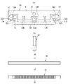
始めに、図3を参照して、本発明の第1の実施の形態に係る加工用治具が使用される加工装置の一例について説明する。図3は、この加工装置の概略の構成を示す斜視図である。この加工装置1は、スライダ部分が一列に配列された棒状の磁気ヘッド用素材であるバーをラッピングする装置である。加工装置1は、テーブル10と、このテーブル10上に設けられた回転ラッピングテーブル11と、この回転ラッピングテーブル11の側方において、テーブル10上に設けられた支柱12と、この支柱12に対してアーム13を介して取り付けられた素材支持部20とを備えている。回転ラッピングテーブル11は、バーに当接するラッピングプレート11aを有している。
【0023】
素材支持部20は、冶具保持部23と、この治具保持部23の前方位置に等間隔に配設された3本の荷重付加棒25A,25B,25Cとを有している。本実施の形態に係る加工用冶具(以下、単に治具と言う。)50は、冶具保持部23に固定されるようになっている。後で詳しく説明するが、治具50には、断面が矩形の孔からなる3つの荷重付加部が設けられている。荷重付加棒25A,25B,25Cの各下端部には、それぞれ、冶具50の各荷重付加部(孔)に挿入される断面が矩形の頭部を有する荷重付加ピンが設けられている。各荷重付加ピンは、それぞれ図示しないアクチュエータによって、上下方向、左右方向(治具50の長手方向)および回転方向に駆動されるようになっている。
【0024】
次に、図1を参照して、本実施の形態に係る治具の構成について説明する。図1は、本実施の形態に係る治具を表し、(a)は治具の正面図、(b)は治具の右側面図、(c)は治具の平面図、(d)は治具の底面図である。これらの図に示したように、本実施の形態に係る治具50は、例えば図3に示したような加工装置1に固定される本体部51と、1方向に長い加工対象物としてのバーを保持するための1方向に長い保持部52と、保持部52と本体部51とを連結する4本の連結部53A〜53Dと、保持部52に連結され、保持部52を変形させるための荷重が付加される3つの荷重付加部54A〜54Cと、荷重付加部54A〜54Cと保持部52とを連結する腕部55A〜55Cとを備えている。
【0025】
本体部51には、長手方向の中央で、且つ上下方向の中央よりも上側の位置に、固定用孔56が形成されている。この固定用孔56には、加工装置1の冶具保持部23に設けられた図示しない治具固定用ピンに対して本体部51を固定するためのボルトが挿通されるようになっている。冶具50は、固定用孔56の位置である1箇所でのみ加工装置1に対して固定されるようになっている。
【0026】
また、本体部51には2つの係合部57,57が形成されている。この係合部57,57には、加工装置1の冶具保持部23に設けられた図示しない2つのガイドピンが係合するようになっている。この係合部57,57は、固定用孔56を中心にして冶具50が回転することを防止するために設けられる。
【0027】
保持部52は、外力が加えられることによってたわむ細長い梁構造になっている。保持部52の下端部には、バーが固定されるバー固定部58が設けられている。バー固定部58には、バーを切断する際に、バー切断用のブレードが入り込む複数の溝が形成されている。保持部52の両端部52a,52bは、本体部51に連結されずに解放されている。
【0028】
治具50は、例えば、ステンレス鋼や、ジルコニア(ZrO2 ),アルミナ(Al2 O3 )等のセラミックによって形成される。
【0029】
本実施の形態では、2つの荷重付加部54A,54Cは、保持部52の長手方向の中央よりも各端部52a,52b側の位置で且つ上下方向の略中央の位置に配置されて、腕部55A,55Cを介して、保持部52の各端部52a,52bから所定の距離だけ中央寄りの位置に連結されている。他の1つの荷重付加部54Bは、本体部51の長手方向の中央で、且つ上下方向の中央よりも下側の位置に配置されている。
【0030】
2つの連結部53A,53Dは、それぞれ、一端部が本体部51に接続され、他端部が荷重付加部54A,54Cと保持部52との連結部分である腕部55A,55Cに接続されている。また、連結部53A,53Dは、可撓性を有する板状をなしている。
【0031】
他の2つの連結部53B,53Cは、それぞれ、一端部が本体部51に接続され、他端部が保持部52に接続されている。また、連結部53B,53Cは、可撓性を有する板状をなしている。
【0032】
次に、図2を参照して、本実施の形態に係る冶具50の作用について説明する。図2は、本実施の形態に係る冶具50の使用状態を示す正面図である。この図に示したように、バー70は、治具50のバー固定部58に対して、バー70の媒体対向面が表側(下側)となるように接着等により固定される。バー70を保持した治具50は、加工装置1に対して固定されると、バー70の被加工面が回転ラッピングテーブル11のラッピングプレート11aに当接するように配置される。この状態で、加工装置1の荷重付加ピンを上下方向、左右方向、回転方向の3方向に駆動することにより、治具50の荷重付加部54A,54B,54Cに対してそれぞれ3方向の荷重を付加することができる。
【0033】
上述のようにして、治具50の荷重付加部54A,54B,54Cに対して種々の方向の荷重を付加することにより、保持部52、バー固定部58およびバー70が変形される。これにより、バー70内の各薄膜磁気ヘッド素子のスロートハイトおよびMRハイトの値を目標とする値となるように制御しながら、バー70の媒体対向面をラッピングすることが可能となる。
【0034】
本実施の形態に係る冶具50では、保持部52の両端部52a,52bが本体部51に連結されずに解放されていることから、保持部52の両端部52a,52bの近傍において、自由な変形が阻害されることなく、片持ち梁構造と同等のたわみ形状を得ることができる。従って、本実施の形態に係る冶具50によれば、保持部52の両端部52a,52bの近傍においても保持部52を望む形状に変形させることが可能になる。その結果、長いバー70を用いる場合であっても、バー70を精度よく加工することが可能になり、その結果、長いバー70に含まれる多くの薄膜磁気ヘッド素子のスロートハイトおよびMRハイトの目標値に対する偏差を小さくすることができる。
【0035】
また、本実施の形態に係る冶具50によれば、各荷重付加部54A,54B,54Cがそれぞれ3方向の荷重を受けることができるので、保持部52を複雑な形状に変形させることが可能になり、薄膜磁気ヘッド素子のスロートハイトおよびMRハイトの高精度な制御が可能になる。
【0036】
ところで、バー70は、薄膜磁気ヘッド素子を含むスライダ部分が複数列に配列されたウェハを一方向に切断して形成されたものである。このバー70は、スライダ部分が一列に配列されたものである。
【0037】
ここで、図4を参照して、薄膜磁気ヘッド素子の構成の一例について説明する。図4は、薄膜磁気ヘッド素子における媒体対向面に垂直な断面を示す断面図である。本例は、書き込み用の誘導型電磁変換素子と読み出し用のMR素子とを積層した構造の複合型の薄膜磁気ヘッド素子の例である。
【0038】
本例における薄膜磁気ヘッド素子71は、アルティック(Al2O3・TiC)等のセラミック材料よりなる基板72と、この基板72の上に形成されたアルミナ(Al2O3)等の絶縁材料よりなる絶縁層73と、この絶縁層73の上に形成された磁性材料よりなる下部シールド層74と、この下部シールド層74の上に形成されたアルミナ等の絶縁材料よりなる下部シールドギャップ膜75と、一端部が媒体対向面(図4における左側の面)に配置されるように、下部シールドギャップ膜75の上に形成された再生用のMR素子76と、下部シールドギャップ膜75の上に形成され、MR素子76に電気的に接続された一対の電極層77と、下部シールドギャップ膜75、MR素子76および電極層77を覆うように形成された上部シールドギャップ膜78と、この上部シールドギャップ膜78の上に形成された磁性材料よりなる上部シールド層兼下部磁極層(以下、下部磁極層と記す。)79とを備えている。MR素子76には、AMR(異方性磁気抵抗効果)素子、GMR(巨大磁気抵抗効果)素子あるいはTMR(トンネル磁気抵抗効果)素子等の磁気抵抗効果を示す感磁膜を用いた素子を用いることができる。
【0039】
薄膜磁気ヘッド素子は、更に、下部磁極層79の上に形成されたアルミナ等の絶縁材料よりなる記録ギャップ層80と、この記録ギャップ層80の上に形成され、例えば熱硬化させたフォトレジストよりなる絶縁層81によって囲われた薄膜コイル82と、絶縁層81の上に形成された磁性材料よりなる上部磁極層83と、この上部磁極層83を覆うように形成されたアルミナ等の絶縁材料よりなる保護層84とを備えている。図示しないが、保護層84の上面には、MR素子76と薄膜コイル82に接続された複数のパッド状の電極が形成されている。
【0040】
上部磁極層83の媒体対向面側の一部である磁極部分と、下部磁極層79の媒体対向面側の一部である磁極部分は、記録ギャップ層80を介して互いに対向している。上部磁極層83の磁極部分は、記録トラック幅に等しい幅を有している。また、上部磁極層83の媒体対向面とは反対側の端部は、記録ギャップ層80に形成されたコンタクトホールを介して下部磁極層79に接続され、磁気的に連結されている。
【0041】
図4に示した薄膜磁気ヘッド素子71において媒体対向面(図における左側の面)が、図3に示した加工装置1によってラッピングされる面である。ラッピングの際、加工装置1は、バー70に含まれる各薄膜磁気ヘッド素子71におけるスロートハイトTHおよびMRハイトMR−hが全て許容誤差の範囲内となるように制御を行う。このような制御は、例えば、特開平2−95572号公報に示されるように、電気的ラッピングガイド(Electrical Lapping Guide:ELG)とMR素子76の抵抗値を監視することによって行われる。電気的ラッピングガイドは、例えば、バー70の長手方向の両端部に配置されるように、薄膜磁気ヘッド素子71の形成の際に、基板72上に形成される。
【0042】
図5は、上述のように、電気的ラッピングガイドとMR素子の抵抗値を監視してラッピングを制御する加工装置の回路構成の一例を示すブロック図である。この例の加工装置は、バー70内の電気的ラッピングガイド(図では、ELGと記す。)85とMR素子76の抵抗値を監視して、治具50の荷重付加部54A,54B,54Cにそれぞれ3方向の荷重を付加するための9つアクチュエータ91〜99を制御する制御装置86と、図示しないコネクタを介して、バー70内の複数の電気的ラッピングガイド85および複数のMR素子76に接続され、これらの電気的ラッピングガイド85およびMR素子76のいずれかを選択的に制御装置86に接続するマルチプレクサ87とを備えている。
【0043】
この加工装置では、制御装置86は、マルチプレクサ87を介して、バー70内の電気的ラッピングガイド85およびMR素子76の抵抗値を監視して、アクチュエータ91〜99を制御する。制御装置86は、始めは、電気的ラッピングガイド85の抵抗値を監視することによって、粗仕上げを行い、その後、各MR素子76の抵抗値を監視することによって、各薄膜磁気ヘッド素子71におけるスロートハイトTHおよびMRハイトMR−hが全て許容誤差の範囲内となるように制御を行う。
【0044】
次に、図6ないし図10を参照して、本実施の形態に係る冶具50を用いて加工が施されるバー70をウェハより切り出す方法の例について説明する。以下の例では、薄膜磁気ヘッド素子を含むスライダ部分が複数列に配列された円板状のウェハより、互いに幅の異なる複数種類のブロックを形成する。各ブロックは、複数列に配列されたスライダ部分を含み一定の幅を有する。バーは、ブロックを1方向に切断して形成される。
【0045】
以下の例において、円板状のウェハの直径は、例えば、76.2mm(3インチ)、152.4mm(6インチ)または203.2mm(8インチ)である。以下、直径が76.2mm(3インチ)、152.4mm(6インチ)、203.2mm(8インチ)のウェハを、それぞれ、3インチウェハ、6インチウェハ、8インチウェハと言う。
【0046】
図6は、3インチウェハより3種類のブロックを切り出す場合におけるブロックの配置の一例を示す説明図である。この例では、3インチウェハ101aより、3種類のブロック111A,111B,111Cを切り出している。なお、図6ないし図10では、ブロック111A,111B,111Cを、それぞれ簡略的に符号A,B,Cでも表している。図6において、スライダ部分の列は左右方向に延び、このスライダ部分の列が上下方向に複数並んでいる。また、ブロック111A,111B,111Cの幅とは、図6においてブロック111A,111B,111Cの左右方向の長さである。ブロック111A,111B,111Cの中では、ブロック111Aの幅が最も大きく、次にブロック111Bの幅が大きく、ブロック111Cの幅が最も小さくなっている。
【0047】
図6に示した例では、3インチウェハ101a内の上下方向の中央部分よりブロック111Aが切り出され、ブロック111Aの上側および下側よりそれぞれブロック111Bが切り出され、更にその上側および下側よりそれぞれブロック111Cが切り出されている。3インチウェハ101aの外周から内側へ向かって所定の幅の領域は、ブロックとする部分から除いている。
【0048】
ブロック111Aの幅は、例えば69.6mm±5%とする。ブロック111Bの幅は、例えば57.6mm±5%とする。ブロック111Cの幅は、例えば38.4mm±5%とする。各ブロック111A,111B,111Cにおいて、幅方向の両端から内側へ向かって所定(スライダ部分2個分程度)の幅の領域内のスライダ部分は無効とし、残りのスライダ部分を有効とする。
【0049】
図7は、3インチウェハより2種類のブロックを切り出す場合におけるブロックの配置の一例を示す説明図である。この例では、3インチウェハ101aより、2種類のブロック111A,111Bを切り出している。3インチウェハ101a内におけるブロック111A,111Bの位置は、図6に示した例と同様である。
【0050】
図8は、6インチウェハより2種類のブロックを切り出す場合におけるブロックの配置の一例を示す説明図である。図8に示した例では、6インチウェハ101b内の上下方向の中央部分より、左右に方向に並ぶ2つのブロック111A1が切り出されている。また、各ブロック111A1の上側および下側ではブロック111Bが切り出されている。また、上下の各ブロック111Bの上側および下側ではブロック111A2が切り出されている。なお、ブロック111A1,111A2はブロック111Aと同じ種類に属し、その幅はブロック111Aと同じである。
【0051】
図9は、8インチウェハより2種類のブロックを切り出す場合におけるブロックの配置の一例を示す説明図である。図9に示した例では、8インチウェハ101c内の上下方向の中央部分において、左右方向の中央部分よりブロック111B11が切り出され、その左右両側よりそれぞれブロック111A11が切り出されている。また、ブロック111A11,111B11の上側および下側では、左右方向の中央部分よりブロック111A12が切り出され、その左右両側よりそれぞれブロック111B12が切り出されている。また、上下の各ブロック111A12,111B12の上側および下側では、左右方向に並ぶ3つのブロック111B13が切り出されている。また、上下の各ブロック111B13の上側および下側では、左右方向に並ぶ2つのブロック111A13が切り出されている。また、上下の各ブロック111A13の上側および下側では、左右方向に並ぶ2つのブロック111B14が切り出されている。また、上下の各ブロック111B14の上側および下側ではブロック111A14が切り出されている。
【0052】
なお、ブロック111A11,111A12,111A13,111A14は、ブロック111Aと同じ種類に属し、その幅はブロック111Aと同じである。同様に、ブロック111B11,111B12,111B13,111B14はブロック111Bと同じ種類に属し、その幅はブロック111Bと同じである。
【0053】
図10は、8インチウェハより2種類のブロックを切り出す場合におけるブロックの配置の他の例を示す説明図である。図10に示した例では、8インチウェハ101c内の上下方向の中央部分において、左右方向の中央部分よりブロック111A21が切り出され、その左右両側よりそれぞれブロック111B21が切り出されている。また、ブロック111A21,111B21の上側および下側では、左右方向に並ぶ3つのブロック111B22が切り出されている。また、上下の各ブロック111B22の上側および下側では、左右方向に並ぶ2つのブロック111A22が切り出されている。また、上下の各ブロック111A22の上側および下側では、左右方向に並ぶ2つのブロック111B23が切り出されている。また、上下の各ブロック111B23の上側および下側ではブロック111A23が切り出されている。
【0054】
なお、ブロック111A21,111A22,111A23は、ブロック111Aと同じ種類に属し、その幅はブロック111Aと同じである。同様に、ブロック111B21,111B22,111B23は、ブロック111Bと同じ種類に属し、その幅はブロック111Bと同じである。
【0055】
図6ないし図10に示した例のようにしてウェハより切り出された2種類または3種類のブロックを切断してバーを形成することにより、長さが69.6mm±5%と57.6mm±5%の2種類のバー、または、これらに長さが38.4mm±5%のバーを加えた3種類のバーが得られる。本実施の形態に係る冶具50は、このような複数種類のバーに対して共通に使用される。
【0056】
以下、構造解析シミュレーションの結果を参照して、本実施の形態に係る冶具50の作用および効果について詳しく説明する。
【0057】
まず、構造解析シミュレーションにおいて本実施の形態に係る冶具50と比較するために用いた2つの比較例の冶具について説明する。図11は第1の比較例の冶具151を示す正面図、図12は第2の比較例の冶具152を示す正面図である。
【0058】
図11に示した第1の比較例の冶具151では、保持部52の両端部が連結部53A,53Dを介して本体部51に連結されている。また、この冶具151における保持部52およびバー固定部58は、長さが約50mmのバーについて使用するのに適するように設計されており、本実施の形態に係る冶具50における保持部52およびバー固定部58に比べて短くなっている。また、この冶具151では、保持部52が短い分、連結部53A,53Dが長くなっている。
【0059】
図12に示した第2の比較例の冶具152における保持部52およびバー固定部58は、長さが約70mmのバーについて使用できるように、第1の比較例の冶具151における保持部52およびバー固定部58よりも長く、本実施の形態に係る冶具50における保持部52およびバー固定部58と同程度の長さになっている。また、この冶具152においても、保持部52の両端部は連結部53A,53Dを介して本体部51に連結されている。また、この冶具152では、第1の比較例の冶具151に比べて、保持部52が長い分、連結部53A,53Dが短くなっている。
【0060】
図13は、図11に示した第1の比較例の冶具151に対する構造解析シミュレーションの結果を示したものである。このシミュレーションでは、冶具151の荷重付加部54A,54Cにそれぞれ上方向に9.8N(=1kgf)の荷重を付加し、荷重付加部54Bに下方向に9.8N(=1kgf)の荷重を付加している。このシミュレーションの結果では、保持部52においてほぼ理想的なたわみが得られている。これは、保持部52の両端部近傍において保持部52の自由な変形が阻害されない程度に、連結部53A,53Dが十分長いためである。
【0061】
図14は、図12に示した第2の比較例の冶具152に対する構造解析シミュレーションの結果を示したものである。荷重の付加の条件は、図13の場合と同様である。このシミュレーションの結果では、保持部52の両端部近傍において保持部52の自由な変形が阻害されている。このように、保持部52の両端部を連結部53A,53Dを介して本体部51に連結した構造では、保持部52を長くすると、その分、連結部53A,53Dが短くなり、その結果、保持部52の両端部近傍において保持部52の自由な変形が阻害されて、保持部52の両端部近傍において理想的なたわみが得られないことが分かる。
【0062】
また、構造解析シミュレーションにより、第1の比較例や第2の比較例のように保持部52の両端部を連結部53A,53Dを介して本体部51に連結した構造では、保持部52の長さが本体部51の長さの約65%以内の場合には保持部52においてほぼ理想的なたわみが得られるが、保持部52の長さが本体部51の長さの約65%を超えると保持部52の両端部近傍において理想的なたわみが得られないことが分かった。
【0063】
図15は、図1に示した本実施の形態に係る冶具50に対する構造解析シミュレーションの結果を示したものである。荷重の付加の条件は、図13の場合と同様である。このシミュレーションの結果では、保持部52において理想的なたわみが得られている。このように、保持部52の両端部52a,52bが本体部51に連結されずに解放された構造とすることにより、保持部52を長くしても、保持部52において理想的なたわみが得られることが分かる。また、構造解析シミュレーションにより、本実施の形態に係る冶具50では、保持部52の長さが本体部51の長さの約85%以内の場合に、保持部52においてほぼ理想的なたわみが得られることが分かった。
【0064】
次に、図16ないし図25を参照して、本実施の形態に係る冶具50が、図12に示した第2の比較例の冶具152に比べて、保持部52においてより理想的なたわみが得られることを定量的に示す2つのシミュレーションの結果について説明する。
【0065】
図16ないし図20は第1のシミュレーションに係るものである。図16は、第1のシミュレーションにおいて作りたい保持部52の変位曲線(以下、理想曲線と言う。)を示したものである。図16において、横軸は保持部52における長手方向の位置を表し、縦軸は保持部52の垂直方向の変位を表している。
【0066】
図17は、第2の比較例の冶具152で得られる保持部52の変位曲線を実線で示し、理想曲線を破線で示したものである。図17における横軸と縦軸は図16と同様である。図18は、図17に示した第2の比較例の冶具152で得られる保持部52の変位曲線と理想曲線との偏差を示したものである。図18において、横軸は保持部52における長手方向の位置を表し、縦軸は偏差を表している。
【0067】
図19は、本実施の形態に係る冶具50で得られる保持部52の変位曲線を示したものである。図19における横軸と縦軸は図16と同様である。図20は、図19に示した本実施の形態に係る冶具50で得られる保持部52の変位曲線と図16に示した理想曲線との偏差を示したものである。図20における横軸と縦軸は図18と同様である。
【0068】
図18と図20を比較すると、本実施の形態に係る冶具50が、第2の比較例の冶具152に比べて、保持部52においてより理想的なたわみが得られることがよく分かる。
【0069】
図21ないし図25は第2のシミュレーションに係るものである。図21は、第2のシミュレーションにおいて作りたい保持部52の変位曲線(理想曲線)を示したものである。図21において、横軸は保持部52における長手方向の位置を表し、縦軸は保持部52の垂直方向の変位を表している。
【0070】
図22は、第2の比較例の冶具152で得られる保持部52の変位曲線を実線で示し、理想曲線を破線で示したものである。図22における横軸と縦軸は図21と同様である。図23は、図22に示した第2の比較例の冶具152で得られる保持部52の変位曲線と理想曲線との偏差を示したものである。図23において、横軸は保持部52における長手方向の位置を表し、縦軸は偏差を表している。
【0071】
図24は、本実施の形態に係る冶具50で得られる保持部52の変位曲線を示したものである。図24における横軸と縦軸は図21と同様である。図25は、図24に示した本実施の形態に係る冶具50で得られる保持部52の変位曲線と図21に示した理想曲線との偏差を示したものである。図25における横軸と縦軸は図23と同様である。
【0072】
図23と図25を比較すると、本実施の形態に係る冶具50が、第2の比較例の冶具152に比べて、保持部52においてより理想的なたわみが得られることが分かる。
【0073】
以上説明したように、本実施の形態に係る冶具50によれば、保持部52の両端部52a,52bが本体部51に連結されずに解放されているので、保持部52の両端部52a,52bの近傍において自由な変形が阻害されることがなく、保持部52の両端部52a,52bの近傍においても保持部52を望む形状に変形させることが可能になる。従って、本実施の形態によれば、長いバー70を用いる場合であっても、バー70を精度よく加工することが可能になる。その結果、長いバー70に含まれる多くの薄膜磁気ヘッド素子のスロートハイトおよびMRハイトの目標値に対する偏差を小さくでき、薄膜磁気ヘッドの歩留りを向上させることができる。
【0074】
[第2の実施の形態]
次に、図26を参照して、本発明の第2の実施の形態に係る加工用冶具について説明する。図26は、本実施の形態に係る加工用冶具250の使用状態を示す正面図である。本実施の形態に係る冶具250では、荷重付加部54Bと連結部53Bとの間の位置に、荷重付加部54Dと、この荷重付加部54Dと保持部52とを連結する腕部55Dとが設けられ、荷重付加部54Bと連結部53Cとの間の位置に、荷重付加部54Eと、この荷重付加部54Eと保持部52とを連結する腕部55Eとが設けられている。また、本実施の形態に係る冶具250では、荷重付加部54A〜54Eは、断面がほぼ円形の孔によって構成されている。これらの荷重付加部54A〜54Eは上下方向に駆動されるようになっている。なお、この冶具250を使用する加工装置は、5つの荷重付加部54A〜54Eに独立に荷重を付加できる5本の荷重付加棒を有するものとする。
【0075】
本実施の形態では、荷重付加部54A〜54Eは上下方向に変位するだけであるが、第1の実施の形態に係る冶具50に比べて荷重付加部の数が多いので、第1の実施の形態と同様に、保持部52を複雑な形状に変形させることが可能になり、薄膜磁気ヘッド素子のスロートハイトおよびMRハイトの高精度な制御が可能になる。
【0076】
本実施の形態におけるその他の構成、作用および効果は、第1の実施の形態と同様である。
【0077】
[第3の実施の形態]
次に、図27を参照して、本発明の第3の実施の形態に係る加工用冶具について説明する。図27は、本実施の形態に係る加工用冶具350の使用状態を示す正面図である。本実施の形態に係る冶具350では、荷重付加部54Aと連結部53Bとの間の位置に、荷重付加部154Aと、この荷重付加部154Aと保持部52とを連結する腕部155Aとが設けられ、荷重付加部54Bと連結部53Bとの間の位置に、荷重付加部154Bと、この荷重付加部154Bと保持部52とを連結する腕部155Bとが設けられ、荷重付加部54Bと連結部53Cとの間の位置に、荷重付加部154Cと、この荷重付加部154Cと保持部52とを連結する腕部155Cとが設けられ、荷重付加部54Bと連結部53Dとの間の位置に、荷重付加部154Dと、この荷重付加部154Dと保持部52とを連結する腕部155Dとが設けられている。また、本実施の形態に係る冶具350では、荷重付加部54A〜54C,154A〜154Dは、断面がほぼ円形の孔によって構成されている。これらの荷重付加部54A〜54C,154A〜154Dは上下方向に駆動されるようになっている。なお、この冶具350を使用する加工装置は、7つの荷重付加部54A〜54C,154A〜154Dに独立に荷重を付加できる7本の荷重付加棒を有するものとする。
【0078】
本実施の形態では、第2の実施の形態に係る冶具250に比べて荷重付加部の数が多いので、第2の実施の形態に係る冶具250よりも、保持部52を複雑な形状に変形させることが可能になり、薄膜磁気ヘッド素子のスロートハイトおよびMRハイトのより高精度な制御が可能になる。
【0079】
本実施の形態におけるその他の構成、作用および効果は、第1または第2の実施の形態と同様である。
【0080】
なお、本発明は、上記各実施の形態に限定されず、種々の変更が可能である。例えば、本発明は、加工として、ラッピング以外の加工、例えばポリシングや、グラインディングを行う場合にも適用することができる。また、本発明は、加工が施される加工対象物が薄膜磁気ヘッド以外の場合にも適用することができる。
【0081】
【発明の効果】
以上説明したように本発明の加工用治具によれば、保持部の両端部が本体部に連結されずに解放されているので、保持部の両端部近傍においても保持部を望む形状に変形させることが可能になり、長い加工対象物でも精度よく加工することが可能になるという効果を奏する。
【図面の簡単な説明】
【図1】本発明の第1の実施の形態に係る治具を示す図である。
【図2】本発明の第1の実施の形態に係る治具の使用状態を示す正面図である。
【図3】本発明の第1の実施の形態に係る治具が使用される加工装置の一例を示す斜視図である。
【図4】薄膜磁気ヘッド素子の構成の一例を示す断面図である。
【図5】加工装置の回路構成の一例を示すブロック図である。
【図6】3インチウェハより3種類のブロックを切り出す場合におけるブロックの配置の一例を示す説明図である。
【図7】3インチウェハより2種類のブロックを切り出す場合におけるブロックの配置の一例を示す説明図である。
【図8】6インチウェハより2種類のブロックを切り出す場合におけるブロックの配置の一例を示す説明図である。
【図9】8インチウェハより2種類のブロックを切り出す場合におけるブロックの配置の一例を示す説明図である。
【図10】8インチウェハより2種類のブロックを切り出す場合におけるブロックの配置の他の例を示す説明図である。
【図11】本発明の第1の実施の形態に係る治具に対する第1の比較例の冶具を示す正面図である。
【図12】本発明の第1の実施の形態に係る治具に対する第2の比較例の冶具を示す正面図である。
【図13】第1の比較例の冶具に対する構造解析シミュレーションの結果を示す説明図である。
【図14】第2の比較例の冶具に対する構造解析シミュレーションの結果を示す説明図である。
【図15】本発明の第1の実施の形態に係る冶具に対する構造解析シミュレーションの結果を示す説明図である。
【図16】第1のシミュレーションにおいて作りたい保持部の変位曲線を示す説明図である。
【図17】第1のシミュレーションにおいて第2の比較例の冶具で得られる保持部の変位曲線を示す説明図である。
【図18】第1のシミュレーションにおいて第2の比較例の冶具で得られる保持部の変位曲線と理想曲線との偏差を示す説明図である。
【図19】第1のシミュレーションにおいて本発明の第1の実施の形態に係る冶具で得られる保持部の変位曲線を示す説明図である。
【図20】第1のシミュレーションにおいて本発明の第1の実施の形態に係る冶具で得られる保持部の変位曲線と理想曲線との偏差を示す説明図である。
【図21】第2のシミュレーションにおいて作りたい保持部の変位曲線を示す説明図である。
【図22】第2のシミュレーションにおいて第2の比較例の冶具で得られる保持部の変位曲線を示す説明図である。
【図23】第2のシミュレーションにおいて第2の比較例の冶具で得られる保持部の変位曲線と理想曲線との偏差を示す説明図である。
【図24】第2のシミュレーションにおいて本発明の第1の実施の形態に係る冶具で得られる保持部の変位曲線を示す説明図である。
【図25】第2のシミュレーションにおいて本発明の第1の実施の形態に係る冶具で得られる保持部の変位曲線と理想曲線との偏差を示す説明図である。
【図26】本発明の第2の実施の形態に係る加工用冶具の使用状態を示す正面図である。
【図27】本発明の第3の実施の形態に係る加工用冶具の使用状態を示す正面図である。
【符号の説明】
50…加工用治具、51…本体部、52…保持部、53A〜53D…連結部、54A〜54C…荷重付加部、55A〜55C…腕部、56…固定用孔、57…係合部、58…バー固定部。[0001]
BACKGROUND OF THE INVENTION
The present invention relates to a processing jig for holding an object to be processed by a processing apparatus.
[0002]
[Prior art]
A floating thin-film magnetic head used in a magnetic disk device or the like is generally in the form of a slider in which a thin-film magnetic head element is formed in a subsequent stage. The slider generally has a rail portion whose surface is a medium facing surface (air bearing surface), and has a tapered portion or a step portion near the end on the air inflow side, and flows from the tapered portion or the step portion. The air flow causes the rail portion to slightly float from the surface of a recording medium such as a magnetic disk.
[0003]
As the thin film magnetic head element, a composite type thin film magnetic head element having a structure in which an inductive electromagnetic transducer element for writing and a magnetoresistive element for reading (hereinafter referred to as MR (Magneto Resistive)) element are stacked. Widely used.
[0004]
A slider generally has a rod shape in which a portion of a slider including thin-film magnetic head elements (hereinafter referred to as a slider portion) is cut in one direction and a slider portion is arranged in a row. The magnetic head material (hereinafter referred to as a bar) is formed, and a process such as lapping (polishing) is performed on the surface (hereinafter referred to as the medium facing surface for convenience) of the bar. And then manufactured by cutting the bar and separating it into sliders.
[0005]
In general, in order to stabilize the output characteristics of a thin film magnetic head, it is important to keep the distance between the magnetic pole portion of the thin film magnetic head and the surface of the recording medium at a very small constant value. For this purpose, the flatness of the medium facing surface of the thin film magnetic head is accurately stored within a predetermined value to stabilize the flying height, and the throat height and MR height values of the thin film magnetic head are within a predetermined range. This is an important requirement in the processing of thin film magnetic heads. The throat height refers to the length (height) from the end on the medium facing surface side to the end on the opposite side of the magnetic pole portion in the inductive electromagnetic transducer. The MR height refers to the length (height) from the end of the MR element on the medium facing surface side to the opposite end.
[0006]
There are various methods for wrapping the medium facing surface so that the throat height and MR height values of the thin-film magnetic head become target values, but the method that can be performed with high accuracy and is generally performed is as follows. The method is as follows. In other words, this method has a function for automatically lapping while deforming the bar bonded to the jig by applying an appropriate load to the jig with a processing jig having the functions described later. It is a method of using a wrapping device with it.
[0007]
The jig used in this method has a main body fixed to the wrapping device, a holding part that is long in one direction for holding the bar, and a load that is connected to the holding part to deform the holding part. And a plurality of load applying portions. The holding portion has an elongated beam structure that bends when an external force is applied. In this jig, when a load is applied to the load applying portion from the outside, the holding portion is bent, and the deflection of the holding portion can give the bar held by the holding portion.
[0008]
A bar wrapping method using this jig will be described below. In this lapping method, first, the bar is fixed to the holding portion of the jig with an adhesive or the like so that the surface of the bar to be lapped is on the front side.
[0009]
Next, for the bar fixed to the jig, the throat height and MR height values of each thin film magnetic head element in the bar are measured by an optical or electrical method, and the deviation between the measured value and the target value is measured. That is, the necessary polishing amount is calculated.
[0010]
Next, among the wrapping portions corresponding to the respective thin film magnetic head elements in the bar, the portions that require a larger amount of polishing than the portions corresponding to the other thin film magnetic head elements are polished more. In order to do so, the bar is deformed by applying a load to the load application portion so that the polished surface in the portion becomes convex. On the other hand, in the lapping portion corresponding to each thin film magnetic head element in the bar, a portion that requires a smaller amount of polishing compared to the portions corresponding to other thin film magnetic head elements is to be polished as much as possible. The bar is deformed by applying a load to the load applying portion so that the polished surface in the portion becomes concave. Then, the bar is wrapped by pressing the medium facing surface of the bar against the rotating wrapping plate while the bar is deformed.
[0011]
In this way, the throat height and MR height values of each thin film magnetic head element are measured, the deviation between those measured values and the target value, that is, the required polishing amount, is calculated, and the bar is deformed according to the required polishing amount. The throat height and MR height variations in each thin film magnetic head element are corrected by automatically and repeatedly performing a series of operations of wrapping the bar, and finally the throat in each thin film magnetic head element. The height and MR height converge within a predetermined range.
[0012]
U.S. Pat. No. 5,620,356 shows a lapping apparatus for lapping bars as described above. U.S. Pat. No. 5,607,340 shows a jig for wrapping a magnetic head. Japanese Patent Application Laid-Open No. 2-95572 discloses a wrapping control device that controls the throat height by monitoring the resistance value of the MR element.
[0013]
[Problems to be solved by the invention]
Conventionally, a bar having a predetermined length is cut out from a wafer, and the bar is subjected to processing such as lapping using the processing jig as described above.
[0014]
By the way, in order to increase the processing efficiency, that is, in order to obtain as many products as possible by a single processing, it is desirable to use a bar as long as possible. Therefore, you may want to change the bar length. In such a case, it is also conceivable to change the length or height of the processing jig according to the length of the bar.
[0015]
However, the processing jig is used not only for lapping but in a plurality of steps. In each process, the processing jig is positioned and fixed for use. Therefore, if the length or height of the processing jig is changed, all the positioning and fixing portions of the processing jig in each process must be changed. In addition, when there are a plurality of types of processing jigs having different lengths and heights, it is necessary to devise a positioning and fixing portion of the processing jig so as to be compatible with a plurality of types of processing jigs in each step. Considering such a situation, it is desirable that the shape of the processing jig is constant regardless of the length of the bar.
[0016]
However, in a conventional processing jig as shown in, for example, the aforementioned US Pat. No. 5,607,340, both ends of the holding portion are connected to the main body. In the processing jig having such a shape, free deformation of the holding portion is hindered in the vicinity of both end portions. Therefore, in the conventional processing jig, it is difficult to deform the portions near both ends of the holding portion into a desired shape. As a result, in the conventional processing jig, when a long bar is used, there is a problem that deviations from the target values of the throat height and MR height of the thin film magnetic head element in the vicinity of both ends of the bar increase.
[0017]
The present invention has been made in view of such problems, and an object thereof is to have a holding portion that holds a workpiece that is long in one direction, and to deform the workpiece by deforming the holding portion. An object of the present invention is to provide a processing jig capable of deforming a holding portion into a desired shape even in the vicinity of both end portions of the holding portion so that a long workpiece can be processed with high accuracy.
[0018]
[Means for Solving the Problems]
The processing jig of the present invention is a processing jig that holds a long processing object in one direction and is fixed to a processing apparatus that processes the processing object,
A main body fixed to the processing apparatus;
A holding portion that is long in one direction for holding the workpiece;
A plurality of connecting portions for connecting the holding portion and the main body portion;
Holding partA plurality of load applying portions to which a load for deformation is applied;,
A plurality of arm portions connecting each load applying portion and the holding portion;With
Of the connection positions of the plurality of connecting portions and the holding portion and the connection positions of the plurality of arm portions and the holding portion, the two connection positions closest to both ends in the longitudinal direction of the holding portion are the lengths of the holding portions. It is arranged at a position closer to the center in the longitudinal direction by a predetermined distance than both ends in the direction.Is.
[0019]
In the processing jig of the present invention, since both end portions of the holding portion are released without being connected to the main body portion, the holding portion can be deformed into a desired shape even in the vicinity of both end portions of the holding portion. .
[0020]
In the processing jig of the present invention, two of the plurality of load applying portions are respectively located at positions on the end portions side from the center in the longitudinal direction of the holding portion.Arranged,Two of the plurality of connecting portions each have one end connected to the main body and the other end having two load applying portions and a holding portion.Each arm to connect withIt may be connected to. In this case, the two connecting portions may have a plate shape having flexibility.
[0021]
In the processing jig of the present invention, the object to be processed may be a rod-shaped magnetic head material in which portions to be a slider including a thin film magnetic head element are arranged in a line.
[0022]
DETAILED DESCRIPTION OF THE INVENTION
Hereinafter, embodiments of the present invention will be described in detail with reference to the drawings.
[First Embodiment]
First, an example of a processing apparatus in which the processing jig according to the first embodiment of the present invention is used will be described with reference to FIG. FIG. 3 is a perspective view showing a schematic configuration of the processing apparatus. This
[0023]
The
[0024]
Next, the configuration of the jig according to the present embodiment will be described with reference to FIG. FIG. 1 shows a jig according to the present embodiment, where (a) is a front view of the jig, (b) is a right side view of the jig, (c) is a plan view of the jig, and (d) is a plan view of the jig. It is a bottom view of a jig. As shown in these drawings, the
[0025]
A fixing
[0026]
The
[0027]
The holding
[0028]
The
[0029]
In the present embodiment, the two
[0030]
One end of each of the two connecting
[0031]
Each of the other two connecting
[0032]
Next, with reference to FIG. 2, the effect | action of the
[0033]
As described above, by applying loads in various directions to the
[0034]
In the
[0035]
In addition, according to the
[0036]
Incidentally, the
[0037]
Here, an example of the configuration of the thin film magnetic head element will be described with reference to FIG. FIG. 4 is a cross-sectional view showing a cross section perpendicular to the medium facing surface in the thin film magnetic head element. This example is an example of a composite type thin film magnetic head element having a structure in which an inductive electromagnetic transducer for writing and an MR element for reading are stacked.
[0038]
The thin film
[0039]
The thin film magnetic head element further includes a
[0040]
A magnetic pole portion that is a part of the upper
[0041]
In the thin film
[0042]
FIG. 5 is a block diagram illustrating an example of a circuit configuration of a processing apparatus that controls the lapping by monitoring the resistance values of the electrical lapping guide and the MR element as described above. The processing apparatus in this example monitors the resistance values of the electrical lapping guide (ELG in the figure) 85 and the
[0043]
In this processing apparatus, the
[0044]
Next, an example of a method for cutting out the
[0045]
In the following examples, the diameter of the disk-shaped wafer is, for example, 76.2 mm (3 inches), 152.4 mm (6 inches), or 203.2 mm (8 inches). Hereinafter, wafers having a diameter of 76.2 mm (3 inches), 152.4 mm (6 inches), and 203.2 mm (8 inches) are referred to as a 3 inch wafer, a 6 inch wafer, and an 8 inch wafer, respectively.
[0046]
FIG. 6 is an explanatory diagram showing an example of block arrangement when three types of blocks are cut out from a 3-inch wafer. In this example, three types of
[0047]
In the example shown in FIG. 6, the
[0048]
The width of the
[0049]
FIG. 7 is an explanatory diagram showing an example of the arrangement of blocks when cutting out two types of blocks from a 3-inch wafer. In this example, two types of
[0050]
FIG. 8 is an explanatory diagram showing an example of the arrangement of blocks when cutting out two types of blocks from a 6-inch wafer. In the example shown in FIG. 8, two blocks 111 </ b> A arranged in the horizontal direction from the central portion in the vertical direction in the 6-inch wafer 101 b.1Is cut out. Each
[0051]
FIG. 9 is an explanatory diagram showing an example of block arrangement when two types of blocks are cut out from an 8-inch wafer. In the example shown in FIG. 9, in the central portion in the vertical direction in the 8-
[0052]
[0053]
FIG. 10 is an explanatory diagram showing another example of the arrangement of blocks when cutting out two types of blocks from an 8-inch wafer. In the example shown in FIG. 10, in the central portion in the vertical direction in the 8-
[0054]
[0055]
By cutting the two or three types of blocks cut from the wafer as in the example shown in FIGS. 6 to 10 to form bars, the lengths are 69.6 mm ± 5% and 57.6 mm ± Two bars of 5%, or three bars obtained by adding a bar having a length of 38.4 mm ± 5% are obtained. The
[0056]
Hereinafter, with reference to the result of the structural analysis simulation, the operation and effect of the
[0057]
First, two comparative examples of jigs used for comparison with the
[0058]
In the
[0059]
The holding
[0060]
FIG. 13 shows the result of the structural analysis simulation for the
[0061]
FIG. 14 shows the result of the structural analysis simulation for the
[0062]
Further, in the structure in which both end portions of the holding
[0063]
FIG. 15 shows the result of the structural analysis simulation for the
[0064]
Next, referring to FIGS. 16 to 25, the
[0065]
16 to 20 relate to the first simulation. FIG. 16 shows a displacement curve (hereinafter referred to as an ideal curve) of the holding
[0066]
FIG. 17 shows a displacement curve of the holding
[0067]
FIG. 19 shows a displacement curve of the holding
[0068]
Comparing FIG. 18 and FIG. 20, it can be seen that the
[0069]
21 to 25 relate to the second simulation. FIG. 21 shows a displacement curve (ideal curve) of the holding
[0070]
FIG. 22 shows a displacement curve of the holding
[0071]
FIG. 24 shows a displacement curve of the holding
[0072]
Comparing FIG. 23 and FIG. 25, it can be seen that the
[0073]
As described above, according to the
[0074]
[Second Embodiment]
Next, with reference to FIG. 26, a processing jig according to a second embodiment of the present invention will be described. FIG. 26 is a front view showing a usage state of the
[0075]
In the present embodiment, the
[0076]
Other configurations, operations, and effects in the present embodiment are the same as those in the first embodiment.
[0077]
[Third Embodiment]
Next, a processing jig according to a third embodiment of the present invention will be described with reference to FIG. FIG. 27 is a front view showing a usage state of the
[0078]
In this embodiment, since the number of load application portions is larger than that of the
[0079]
Other configurations, operations, and effects in the present embodiment are the same as those in the first or second embodiment.
[0080]
In addition, this invention is not limited to said each embodiment, A various change is possible. For example, the present invention can also be applied to processing other than lapping, such as polishing or grinding, as processing. The present invention can also be applied to a case where the object to be processed is not a thin film magnetic head.
[0081]
【The invention's effect】
As described above, according to the processing jig of the present invention, since both ends of the holding part are released without being connected to the main body part, the holding part is deformed into a desired shape in the vicinity of both ends of the holding part. Thus, it is possible to accurately process even a long workpiece.
[Brief description of the drawings]
FIG. 1 is a view showing a jig according to a first embodiment of the present invention.
FIG. 2 is a front view showing a usage state of the jig according to the first embodiment of the present invention.
FIG. 3 is a perspective view showing an example of a processing apparatus in which the jig according to the first embodiment of the present invention is used.
FIG. 4 is a cross-sectional view showing an example of the configuration of a thin film magnetic head element.
FIG. 5 is a block diagram illustrating an example of a circuit configuration of a processing apparatus.
FIG. 6 is an explanatory diagram showing an example of the arrangement of blocks when three types of blocks are cut out from a 3-inch wafer.
FIG. 7 is an explanatory diagram showing an example of the arrangement of blocks when cutting out two types of blocks from a 3-inch wafer.
FIG. 8 is an explanatory diagram showing an example of block arrangement when two types of blocks are cut out from a 6-inch wafer.
FIG. 9 is an explanatory diagram showing an example of the arrangement of blocks when cutting out two types of blocks from an 8-inch wafer.
FIG. 10 is an explanatory diagram showing another example of block arrangement when cutting out two types of blocks from an 8-inch wafer.
FIG. 11 is a front view showing a jig of a first comparative example for the jig according to the first embodiment of the present invention.
FIG. 12 is a front view showing a jig of a second comparative example with respect to the jig according to the first embodiment of the present invention.
FIG. 13 is an explanatory diagram showing the results of a structural analysis simulation for the jig of the first comparative example.
FIG. 14 is an explanatory diagram showing a result of a structural analysis simulation for a jig of a second comparative example.
FIG. 15 is an explanatory diagram showing a result of structural analysis simulation for the jig according to the first embodiment of the present invention.
FIG. 16 is an explanatory diagram showing a displacement curve of a holding portion that is to be created in the first simulation.
FIG. 17 is an explanatory diagram showing a displacement curve of the holding portion obtained by the jig of the second comparative example in the first simulation.
FIG. 18 is an explanatory diagram showing a deviation between the displacement curve of the holding portion and the ideal curve obtained with the jig of the second comparative example in the first simulation.
FIG. 19 is an explanatory diagram showing a displacement curve of the holding portion obtained by the jig according to the first embodiment of the present invention in the first simulation.
FIG. 20 is an explanatory diagram showing a deviation between the displacement curve of the holding portion and the ideal curve obtained by the jig according to the first embodiment of the present invention in the first simulation.
FIG. 21 is an explanatory diagram showing a displacement curve of a holding portion that is desired to be created in the second simulation.
FIG. 22 is an explanatory diagram showing a displacement curve of a holding part obtained by the jig of the second comparative example in the second simulation.
FIG. 23 is an explanatory diagram showing a deviation between the displacement curve of the holding portion and the ideal curve obtained with the jig of the second comparative example in the second simulation.
FIG. 24 is an explanatory diagram showing a displacement curve of the holding portion obtained by the jig according to the first embodiment of the present invention in the second simulation.
FIG. 25 is an explanatory diagram showing a deviation between the displacement curve of the holding portion and the ideal curve obtained by the jig according to the first embodiment of the present invention in the second simulation.
FIG. 26 is a front view showing a usage state of the processing jig according to the second embodiment of the present invention.
FIG. 27 is a front view showing a usage state of the processing jig according to the third embodiment of the present invention.
[Explanation of symbols]
DESCRIPTION OF
Claims (4)
前記加工装置に固定される本体部と、
前記加工対象物を保持するための1方向に長い保持部と、
前記保持部と前記本体部とを連結する複数の連結部と、
前記保持部を変形させるための荷重が付加される複数の荷重付加部と、
前記各荷重付加部と前記保持部とを連結する複数の腕部とを備え、
前記複数の連結部と前記保持部との各接続位置および前記複数の腕部と前記保持部との各接続位置のうち、それぞれ前記保持部の長手方向の両端部に最も近い2つの接続位置は、前記保持部の長手方向の両端部よりも、所定の距離だけ前記長手方向の中央に近い位置に配置されていることを特徴とする加工用治具。A processing jig that holds a long processing object in one direction and is fixed to a processing apparatus that processes the processing object,
A main body fixed to the processing apparatus;
A holding part that is long in one direction for holding the workpiece;
A plurality of connecting portions for connecting the holding portion and the main body portion;
A plurality of load applying portions to which a load for deforming the holding portion is applied ;
A plurality of arm portions connecting the load applying portions and the holding portion ;
Of the connection positions of the plurality of connecting parts and the holding part and the connection positions of the plurality of arm parts and the holding part, the two connection positions closest to the longitudinal ends of the holding part are respectively The processing jig is disposed at a position closer to the center in the longitudinal direction by a predetermined distance than both ends in the longitudinal direction of the holding part .
複数の連結部のうちの2つは、それぞれ、一端部が前記本体部に接続され、他端部が前記2つの荷重付加部と前記保持部とを連結する各腕部に接続されていることを特徴とする請求項1記載の加工用治具。Two of the plurality of load applying portions are respectively arranged at positions on the respective end portions side of the longitudinal center of the holding portion ,
Two of the plurality of connecting portions each have one end connected to the main body and the other end connected to each arm connecting the two load applying portions and the holding portion. The processing jig according to claim 1, wherein:
Priority Applications (4)
| Application Number | Priority Date | Filing Date | Title |
|---|---|---|---|
| JP36218899A JP3628571B2 (en) | 1999-12-21 | 1999-12-21 | Processing jig |
| US09/708,536 US6447367B1 (en) | 1999-12-21 | 2000-11-09 | Processing jig |
| SG200006505A SG91888A1 (en) | 1999-12-21 | 2000-11-10 | Processing jig |
| CNB001354965A CN1220572C (en) | 1999-12-21 | 2000-12-20 | Clamp for machining |
Applications Claiming Priority (1)
| Application Number | Priority Date | Filing Date | Title |
|---|---|---|---|
| JP36218899A JP3628571B2 (en) | 1999-12-21 | 1999-12-21 | Processing jig |
Publications (2)
| Publication Number | Publication Date |
|---|---|
| JP2001179616A JP2001179616A (en) | 2001-07-03 |
| JP3628571B2 true JP3628571B2 (en) | 2005-03-16 |
Family
ID=18476210
Family Applications (1)
| Application Number | Title | Priority Date | Filing Date |
|---|---|---|---|
| JP36218899A Expired - Fee Related JP3628571B2 (en) | 1999-12-21 | 1999-12-21 | Processing jig |
Country Status (4)
| Country | Link |
|---|---|
| US (1) | US6447367B1 (en) |
| JP (1) | JP3628571B2 (en) |
| CN (1) | CN1220572C (en) |
| SG (1) | SG91888A1 (en) |
Families Citing this family (16)
| Publication number | Priority date | Publication date | Assignee | Title |
|---|---|---|---|---|
| JP3569474B2 (en) * | 2000-01-13 | 2004-09-22 | Tdk株式会社 | Processing jig |
| JP3537726B2 (en) * | 2000-02-08 | 2004-06-14 | 富士通株式会社 | Method and apparatus for polishing and lapping jig |
| JP3914006B2 (en) * | 2000-06-16 | 2007-05-16 | Tdk株式会社 | Polishing apparatus and method for magnetic head |
| AU2003221014A1 (en) | 2003-03-31 | 2004-10-25 | Fujitsu Limited | Machining method and machining device |
| JP2006116616A (en) * | 2004-10-19 | 2006-05-11 | Shinka Jitsugyo Kk | Polishing tool of slider, polishing device and polishing method |
| US7554767B1 (en) | 2005-07-01 | 2009-06-30 | Western Digital (Fremont), Llc | Electrical lapping guide disposed laterally relative to a shield pedestal |
| US7551406B1 (en) * | 2005-07-01 | 2009-06-23 | Western Digital (Fremont), Llc | Dual electrical lapping guides with common bonding pad |
| JP4795802B2 (en) * | 2006-02-01 | 2011-10-19 | ニッタ・ハース株式会社 | Surface plate of processing apparatus, work piece holding frame material fixed to the surface plate to hold the outer periphery of the work piece, and work piece holding tool using the same |
| JP2009076122A (en) * | 2007-09-19 | 2009-04-09 | Shinka Jitsugyo Kk | Magnetic head and manufacturing method thereof |
| US9427842B1 (en) * | 2012-06-28 | 2016-08-30 | Western Digital Technologies, Inc. | Systems and methods for correcting read/write overlay errors in the manufacture of magnetic transducers for storage drives |
| US9421665B2 (en) | 2014-02-05 | 2016-08-23 | Veeco Instruments, Inc. | Pressure-adjusting lapping element |
| US10843305B2 (en) * | 2014-03-17 | 2020-11-24 | Seagate Technology Llc | Lapping device or carrier with adaptive bending control |
| US9881639B2 (en) * | 2016-06-23 | 2018-01-30 | Western Digital Technologies, Inc. | Within-row wedge angle control for magnetic recording read-write heads |
| US10850364B2 (en) | 2016-06-23 | 2020-12-01 | Western Digital Technologies, Inc. | Within-row stripe height and wedge angle control for magnetic recording read-write heads |
| US10702969B2 (en) | 2016-06-23 | 2020-07-07 | Western Digital Technologies, Inc. | Actuator tilt interposer for within-row lapping mount tool for magnetic recording read-write heads |
| US10792786B2 (en) * | 2018-02-12 | 2020-10-06 | Seagate Technology Llc | Lapping carrier system with optimized carrier insert |
Family Cites Families (12)
| Publication number | Priority date | Publication date | Assignee | Title |
|---|---|---|---|---|
| US4517041A (en) * | 1982-09-30 | 1985-05-14 | Magnetic Peripherals Inc. | Method for attaching a workpiece to a workpiece carrier |
| US4914868A (en) | 1988-09-28 | 1990-04-10 | International Business Machines Corporation | Lapping control system for magnetic transducers |
| US5117589A (en) * | 1990-03-19 | 1992-06-02 | Read-Rite Corporation | Adjustable transfer tool for lapping magnetic head sliders |
| US5203119A (en) * | 1991-03-22 | 1993-04-20 | Read-Rite Corporation | Automated system for lapping air bearing surface of magnetic heads |
| JP2846235B2 (en) * | 1994-02-17 | 1999-01-13 | ティーディーケイ株式会社 | Jig for processing headpiece assembly and method for manufacturing thin-film magnetic head |
| US5620356A (en) | 1995-01-27 | 1997-04-15 | Lackey; Stanley | Row tool balance and bow correction apparatus |
| US5607340A (en) | 1995-06-06 | 1997-03-04 | Lackey; Stanley A. | Row tool |
| JP3688465B2 (en) * | 1997-05-27 | 2005-08-31 | Tdk株式会社 | Processing jig |
| US6045431A (en) * | 1997-12-23 | 2000-04-04 | Speedfam Corporation | Manufacture of thin-film magnetic heads |
| US6315633B1 (en) * | 1998-06-25 | 2001-11-13 | Tdk Corporation | Processing jig |
| JP3693816B2 (en) * | 1998-06-25 | 2005-09-14 | Tdk株式会社 | Processing jig |
| US6174218B1 (en) * | 1999-04-21 | 2001-01-16 | International Business Machines Corporation | Bow compensated lapping |
-
1999
- 1999-12-21 JP JP36218899A patent/JP3628571B2/en not_active Expired - Fee Related
-
2000
- 2000-11-09 US US09/708,536 patent/US6447367B1/en not_active Expired - Fee Related
- 2000-11-10 SG SG200006505A patent/SG91888A1/en unknown
- 2000-12-20 CN CNB001354965A patent/CN1220572C/en not_active Expired - Lifetime
Also Published As
| Publication number | Publication date |
|---|---|
| CN1220572C (en) | 2005-09-28 |
| US6447367B1 (en) | 2002-09-10 |
| SG91888A1 (en) | 2002-10-15 |
| CN1300659A (en) | 2001-06-27 |
| JP2001179616A (en) | 2001-07-03 |
Similar Documents
| Publication | Publication Date | Title |
|---|---|---|
| JP3628571B2 (en) | Processing jig | |
| JP4138777B2 (en) | Lapping guide system and magnetic recording / reproducing head array polishing method | |
| US6261165B1 (en) | Row carrier for precision lapping of disk drive heads and for handling of heads during the slider fab operation | |
| US7911736B2 (en) | Storage device and method of using a head that has a concave surface when powered down | |
| JP3506419B2 (en) | Method of manufacturing magnetic head slider and method of fixing bar | |
| US7086931B2 (en) | Magnetic head bar holding unit, lapping device, and method of lapping medium-opposing surface of thin-film magnetic head | |
| JP3569474B2 (en) | Processing jig | |
| JP4124753B2 (en) | Thin film magnetic head element polishing method, thin film magnetic head element wafer, and thin film magnetic head element polishing apparatus | |
| US7617589B2 (en) | Method of manufacturing slider of thin-film magnetic head | |
| US6865059B2 (en) | Slider of thin-film magnetic head | |
| JP2000011315A (en) | Working jig | |
| JPH1142525A (en) | Machining jig | |
| US7933099B2 (en) | Thin-film magnetic head having electric lapping guide and method of making the same | |
| US20050144776A1 (en) | Method of manufacturing thin-film magnetic head and method of manufacturing slider | |
| US7392580B2 (en) | Method for manufacturing a slider using electromagnetic wave | |
| US6315633B1 (en) | Processing jig | |
| US20090165287A1 (en) | Manufacturing method for magnetic head slider | |
| JP2006172691A (en) | Magnetic head manufacturing method, magnetic head, angle setting device, and lapping device head | |
| US7832085B2 (en) | Method of manufacturing magnetic head and method of manufacturing magnetic head substructure | |
| US7854060B2 (en) | Magnetic head substructure for use for manufacturing a magnetic head | |
| JP3926032B2 (en) | MATERIAL FOR THIN FILM MAGNETIC HEAD, MANUFACTURING METHOD THEREOF, AND METHOD FOR MANUFACTURING THIN FILM MAGNETIC HEAD | |
| US7551407B2 (en) | Thin-film magnetic head, head gimbal assembly and hard disk drive | |
| JP2006294097A (en) | Method and device for polishing thin-film magnetic head, and method for manufacturing thin-film magnetic head | |
| JP2005007571A (en) | Lapping machine and lapping method | |
| US20080222878A1 (en) | Method of manufacturing magnetic head |
Legal Events
| Date | Code | Title | Description |
|---|---|---|---|
| A977 | Report on retrieval |
Free format text: JAPANESE INTERMEDIATE CODE: A971007 Effective date: 20040709 |
|
| A131 | Notification of reasons for refusal |
Free format text: JAPANESE INTERMEDIATE CODE: A131 Effective date: 20040720 |
|
| A521 | Written amendment |
Free format text: JAPANESE INTERMEDIATE CODE: A523 Effective date: 20040914 |
|
| TRDD | Decision of grant or rejection written | ||
| A01 | Written decision to grant a patent or to grant a registration (utility model) |
Free format text: JAPANESE INTERMEDIATE CODE: A01 Effective date: 20041207 |
|
| A61 | First payment of annual fees (during grant procedure) |
Free format text: JAPANESE INTERMEDIATE CODE: A61 Effective date: 20041208 |
|
| R150 | Certificate of patent or registration of utility model |
Free format text: JAPANESE INTERMEDIATE CODE: R150 |
|
| FPAY | Renewal fee payment (event date is renewal date of database) |
Free format text: PAYMENT UNTIL: 20081217 Year of fee payment: 4 |
|
| FPAY | Renewal fee payment (event date is renewal date of database) |
Free format text: PAYMENT UNTIL: 20091217 Year of fee payment: 5 |
|
| FPAY | Renewal fee payment (event date is renewal date of database) |
Free format text: PAYMENT UNTIL: 20091217 Year of fee payment: 5 |
|
| FPAY | Renewal fee payment (event date is renewal date of database) |
Free format text: PAYMENT UNTIL: 20101217 Year of fee payment: 6 |
|
| FPAY | Renewal fee payment (event date is renewal date of database) |
Free format text: PAYMENT UNTIL: 20101217 Year of fee payment: 6 |
|
| FPAY | Renewal fee payment (event date is renewal date of database) |
Free format text: PAYMENT UNTIL: 20111217 Year of fee payment: 7 |
|
| FPAY | Renewal fee payment (event date is renewal date of database) |
Free format text: PAYMENT UNTIL: 20111217 Year of fee payment: 7 |
|
| FPAY | Renewal fee payment (event date is renewal date of database) |
Free format text: PAYMENT UNTIL: 20121217 Year of fee payment: 8 |
|
| FPAY | Renewal fee payment (event date is renewal date of database) |
Free format text: PAYMENT UNTIL: 20121217 Year of fee payment: 8 |
|
| FPAY | Renewal fee payment (event date is renewal date of database) |
Free format text: PAYMENT UNTIL: 20131217 Year of fee payment: 9 |
|
| LAPS | Cancellation because of no payment of annual fees |