JP3614710B2 - Dielectric filter - Google Patents
Dielectric filter Download PDFInfo
- Publication number
- JP3614710B2 JP3614710B2 JP15156299A JP15156299A JP3614710B2 JP 3614710 B2 JP3614710 B2 JP 3614710B2 JP 15156299 A JP15156299 A JP 15156299A JP 15156299 A JP15156299 A JP 15156299A JP 3614710 B2 JP3614710 B2 JP 3614710B2
- Authority
- JP
- Japan
- Prior art keywords
- dielectric
- dielectric substrate
- conductor
- hole
- resonators
- Prior art date
- Legal status (The legal status is an assumption and is not a legal conclusion. Google has not performed a legal analysis and makes no representation as to the accuracy of the status listed.)
- Expired - Lifetime
Links
Images


Landscapes
- Control Of Motors That Do Not Use Commutators (AREA)
Description
【0001】
【発明の属する技術分野】
本発明は、誘電体フィルタの構造に係るもので、特に、その共振器間に容量を付加して所望の特性を得るための導体パターンの構造に関するものである。
【0002】
【従来の技術】
UHF帯からマイクロ波帯といった高周波領域において各種の誘電体フィルタが用いられている。その中でも、貫通孔を具えてその内部に内導体が形成され、外周面に外導体が形成されたTEM共振器を組み合わせた誘電体フィルタが多く用いられている。個別の共振器を接続して構成するものと、誘電体のブロックに一体化されたものとがある。
【0003】
それらの誘電体フィルタにおいては、入出力の結合容量を入出力段の共振器の内導体との間で形成しなければならない。この結合容量を得る手段として、コンデンサを接続したり、コンデンサを形成した誘電体基板を用いる方法がある。また、誘電体を被覆した金属棒を内導体の形成された貫通孔内に挿入したり、内導体の近傍の誘電体に設けた孔に金属棒を挿入したり、外周面に外導体と別の金属皮膜を形成したりする方法がある。
【0004】
誘電体フィルタの分野でも、小型化、薄型化の要求があり、また、周波数帯の上昇にしたがって波長が短くなるため寸法も小さくしなければならない。それに伴って入出力結合容量を得ることも難しくなる。そこで、特開平6−125204号において二枚の誘電体基板を貼り合わせ、その貼り合わせた面に導体パターンを形成して、インピーダンス整合点に直接入出力用の導体パターンを接続する誘電体フィルタが提案されている。また、張り合わせた面に導体パターンを形成して共振器間の結合を調整して帯域通過特性を調整することも試みられている。
【0005】
図3は、その誘電体フィルタの一例の組立前の平面図である。2本の平行な凹溝24を具えた第一の誘電体基板21の凹溝のある面に貼り合わせる平板の第2の誘電体基板22を示したものである。入出力端子と接続される導体パターン26がインピーダンス整合点から引き出される。これと凹溝を有する誘電体基板21を接合するによって、2本の平行な貫通孔を具えた誘電体ブロックが形成される。
【0006】
図4は接着後に導体膜を形成した誘電体フィルタを示す斜視図である。誘電体基板が接着されてなる誘電体ブロックに貫通孔25が形成された構造となっている。この貫通孔25内には内導体が形成され、その貫通孔25の伸びる方向に平行な外周面には外導体27が形成される。外導体に囲まれた端子電極28が形成され、図3に示した導体パターン26と接続される。
【0007】
【発明が解決しようとする課題】
上記のように共振器を一体に形成した誘電体フィルタの帯域通過特性を調整するために、誘電体基板の接合面等に導体パターンを形成してインダクタンスや容量を付加することが考えられている。これらの導体パターンによって容量を付加すると、通過帯域の低域側あるいは高域側に減衰極を形成することができる。
【0008】
容量を十分に得るためには、導体パターンの寸法を十分に大きくする必要がある。しかし、接合面の狭い範囲に形成することが難しく、設計が大きく制約されることになる。また、導体パターンの接続や結合を確実に行う必要がある。本発明は、容量の形成を導体パターンを用いずに実現できる、小型で製造容易な誘電体フィルタを提供するものである。
【0009】
【課題を解決するための手段】
本発明は、接合する基板の誘電率を変えることによって、上記の課題を解決するものである。
【0010】
すなわち、2枚の誘電体基板が接合されて複数の共振器が一体に形成された誘電体フィルタにおいて、
直線的に伸びる複数の平行な凹溝を具えた第1の誘電体基板の凹溝のある表面上に、第1の誘電体基板よりも誘電率の高い平板の第二の誘電体基板が接合されて複数の貫通孔が形成された誘電体ブロックが形成され、
貫通孔内の表面に内導体が形成され、
第一の誘電体基板と第二の誘電体基板の接合面に対向するそれぞれの表面と、凹溝の伸びる方向に平行な両端面に外導体が形成され、
貫通孔の開口する端面の一方に短絡導体が形成されたことに特徴を有するものである。
【0011】
【発明の実施の形態】
凹溝を具えた誘電体基板で形成される低誘電率の誘電体が共振器間に存在するので共振器間の容量性の結合は弱くなり、相対的に誘導性の結合が強くなる。しかし、平板の誘電体基板の誘電率は高いので、共振器の内導体間に容量が発生し、コンデンサで結合したのと同じ状態になる。この容量によって、共振器間がコンデンサ接続されたことになり、通過帯域のいずれかの側に減衰極を得ることができる。
【0012】
【実施例】
以下、図面を参照して、本発明の実施例を説明する。
【0013】
図1は組立後に導体膜を形成した誘電体フィルタを示す斜視図で、図4に示したものと同じ形状である。誘電体基板11、12が接着されてなる誘電体ブロックに貫通孔15が形成された構造となっている。この貫通孔15内には内導体が形成され、その貫通孔15の伸びる方向に平行な外周面には外導体17が形成される。外導体に囲まれた端子電極18が形成され、入出力結合用の導体パターンが接続される。
【0014】
本発明においては、凹溝を具えた誘電体基板11の誘電率を低く、平板の誘電体基板12の誘電率を高くしてある。例えば、凹溝を有する誘電体基板11の誘電率を20ないし30程度とし、平板の誘電体基板12の誘電率を90程度と高くしておく。これによって、電気力線が誘電体基板12に多く引き込まれ、共振器間の容量が増加する。
【0015】
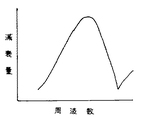
本発明による誘電体フィルタの特性を図2に示す。通過帯域の高域側に減衰極が得られることが確認された。誘電率を変えると減衰極の周波数を変えることができる。
【0016】
本発明は上記の例に限られるものではなく、誘電体基板を接合する誘電体フィルタ全般に適用できる。コムライン型だけでなく、インターディジタル型にも適用できる。。
【0017】
【発明の効果】
本発明によれば、誘電体共振器間の誘導性の結合を相対的に大きくし、更に容量を付加することによって減衰極の形成が可能となる。したがって、他の特性を損なうことなく、任意の帯域通過特性を得ることができる。
【0018】
また、導体パターンが不要になるので、小型で廉価なかつ製造容易な誘電体フィルタが得られる。
【図面の簡単な説明】
【図1】本発明の実施例の斜視図
【図2】本発明による誘電体フィルタの特性の説明図
【図3】従来の誘電体フィルタ例の斜視図
【図4】従来の誘電体フィルタの斜視図
【符号の説明】
11、12:(第1の)誘電体基板
21、22:(第2の)誘電体基板[0001]
BACKGROUND OF THE INVENTION
The present invention relates to a structure of a dielectric filter, and more particularly to a structure of a conductor pattern for obtaining a desired characteristic by adding a capacitance between the resonators.
[0002]
[Prior art]
Various dielectric filters are used in a high frequency region such as a UHF band to a microwave band. Among them, a dielectric filter is often used which is combined with a TEM resonator having a through-hole and an inner conductor formed inside thereof and an outer conductor formed on the outer peripheral surface. Some are configured by connecting individual resonators, while others are integrated into a dielectric block.
[0003]
In these dielectric filters, an input / output coupling capacitance must be formed between the inner conductors of the resonators of the input / output stage. As means for obtaining this coupling capacitance, there are methods of connecting a capacitor or using a dielectric substrate on which a capacitor is formed. Also, insert a metal rod coated with a dielectric into the through hole where the inner conductor is formed, insert a metal rod into a hole provided in the dielectric near the inner conductor, or separate the outer conductor from the outer conductor. There is a method of forming a metal film.
[0004]
In the field of dielectric filters, there is a demand for miniaturization and thinning, and the wavelength has to be shortened as the frequency band increases, so the dimensions must be reduced. Accordingly, it becomes difficult to obtain the input / output coupling capacitance. Japanese Patent Laid-Open No. 6-125204 discloses a dielectric filter in which two dielectric substrates are bonded together, a conductor pattern is formed on the bonded surface, and an input / output conductor pattern is directly connected to an impedance matching point. Proposed. It has also been attempted to adjust the bandpass characteristics by forming a conductor pattern on the bonded surfaces and adjusting the coupling between the resonators.
[0005]
FIG. 3 is a plan view of an example of the dielectric filter before assembly. A flat second
[0006]
FIG. 4 is a perspective view showing a dielectric filter in which a conductor film is formed after bonding. The structure is such that a
[0007]
[Problems to be solved by the invention]
In order to adjust the band-pass characteristics of the dielectric filter in which the resonator is integrally formed as described above, it is considered that a conductor pattern is formed on the joint surface of the dielectric substrate to add inductance and capacitance. . When capacitance is added by these conductor patterns, attenuation poles can be formed on the low band side or high band side of the pass band.
[0008]
In order to obtain a sufficient capacity, it is necessary to sufficiently increase the size of the conductor pattern. However, it is difficult to form the joint surface in a narrow range, and the design is greatly restricted. In addition, it is necessary to securely connect and connect the conductor patterns. The present invention provides a small and easy-to-manufacture dielectric filter capable of realizing the formation of a capacitor without using a conductor pattern.
[0009]
[Means for Solving the Problems]
The present invention solves the above problems by changing the dielectric constant of the substrates to be joined.
[0010]
That is, in a dielectric filter in which a plurality of resonators are integrally formed by joining two dielectric substrates,
A flat second dielectric substrate having a dielectric constant higher than that of the first dielectric substrate is bonded onto the grooved surface of the first dielectric substrate having a plurality of parallel grooves extending linearly. A dielectric block having a plurality of through holes is formed,
An inner conductor is formed on the surface in the through hole,
Outer conductors are formed on each surface facing the bonding surface of the first dielectric substrate and the second dielectric substrate, and on both end faces parallel to the direction in which the groove extends.
This is characterized in that a short-circuit conductor is formed on one end face of the through hole.
[0011]
DETAILED DESCRIPTION OF THE INVENTION
Since a dielectric having a low dielectric constant formed by a dielectric substrate having a concave groove exists between the resonators, the capacitive coupling between the resonators becomes weak, and the inductive coupling becomes relatively strong. However, since the dielectric constant of the flat dielectric substrate is high, a capacitance is generated between the inner conductors of the resonator, which is the same as when coupled by a capacitor. With this capacitance, the resonators are connected by a capacitor, and an attenuation pole can be obtained on either side of the passband.
[0012]
【Example】
Embodiments of the present invention will be described below with reference to the drawings.
[0013]
FIG. 1 is a perspective view showing a dielectric filter in which a conductor film is formed after assembly, and has the same shape as that shown in FIG. A through
[0014]
In the present invention, the dielectric constant of the dielectric substrate 11 having the concave grooves is low, and the dielectric constant of the flat dielectric substrate 12 is high. For example, the dielectric constant of the dielectric substrate 11 having a concave groove is set to about 20 to 30, and the dielectric constant of the flat dielectric substrate 12 is set to about 90. As a result, many lines of electric force are drawn into the dielectric substrate 12 and the capacitance between the resonators increases.
[0015]
The characteristics of the dielectric filter according to the present invention are shown in FIG. It was confirmed that an attenuation pole was obtained on the high side of the passband. The frequency of the attenuation pole can be changed by changing the dielectric constant.
[0016]
The present invention is not limited to the above example, and can be applied to all dielectric filters for bonding dielectric substrates. It can be applied not only to the comb line type but also to the interdigital type. .
[0017]
【The invention's effect】
According to the present invention, it is possible to form an attenuation pole by relatively increasing inductive coupling between dielectric resonators and adding a capacitance. Therefore, an arbitrary band pass characteristic can be obtained without impairing other characteristics.
[0018]
In addition, since no conductor pattern is required, a dielectric filter that is small, inexpensive, and easy to manufacture can be obtained.
[Brief description of the drawings]
FIG. 1 is a perspective view of an embodiment of the present invention. FIG. 2 is an explanatory diagram of characteristics of a dielectric filter according to the present invention. FIG. 3 is a perspective view of an example of a conventional dielectric filter. Perspective view [Explanation of symbols]
11, 12: (first)
Claims (1)
直線的に伸びる複数の平行な凹溝を具えた第1の誘電体基板の凹溝のある表面上に、第1の誘電体基板よりも誘電率の高い平板の第二の誘電体基板が接合されて複数の貫通孔が形成された誘電体ブロックが形成され、
貫通孔内の表面に内導体が形成され、
第一の誘電体基板と第二の誘電体基板の接合面に対向するそれぞれの表面と、凹溝の伸びる方向に平行な両端面に外導体が形成され、
貫通孔の開口する端面の一方に短絡導体が形成されたことを特徴とする誘電体フィルタ。In a dielectric filter in which a plurality of resonators are integrally formed by joining two dielectric substrates,
A flat second dielectric substrate having a dielectric constant higher than that of the first dielectric substrate is bonded onto the grooved surface of the first dielectric substrate having a plurality of parallel grooves extending linearly. A dielectric block having a plurality of through holes is formed,
An inner conductor is formed on the surface in the through hole,
An outer conductor is formed on each surface facing the bonding surface of the first dielectric substrate and the second dielectric substrate, and on both end faces parallel to the extending direction of the groove,
A dielectric filter, characterized in that a short-circuit conductor is formed on one end face of the through hole.
Priority Applications (1)
| Application Number | Priority Date | Filing Date | Title |
|---|---|---|---|
| JP15156299A JP3614710B2 (en) | 1999-05-31 | 1999-05-31 | Dielectric filter |
Applications Claiming Priority (1)
| Application Number | Priority Date | Filing Date | Title |
|---|---|---|---|
| JP15156299A JP3614710B2 (en) | 1999-05-31 | 1999-05-31 | Dielectric filter |
Publications (2)
| Publication Number | Publication Date |
|---|---|
| JP2000341006A JP2000341006A (en) | 2000-12-08 |
| JP3614710B2 true JP3614710B2 (en) | 2005-01-26 |
Family
ID=15521254
Family Applications (1)
| Application Number | Title | Priority Date | Filing Date |
|---|---|---|---|
| JP15156299A Expired - Lifetime JP3614710B2 (en) | 1999-05-31 | 1999-05-31 | Dielectric filter |
Country Status (1)
| Country | Link |
|---|---|
| JP (1) | JP3614710B2 (en) |
-
1999
- 1999-05-31 JP JP15156299A patent/JP3614710B2/en not_active Expired - Lifetime
Also Published As
| Publication number | Publication date |
|---|---|
| JP2000341006A (en) | 2000-12-08 |
Similar Documents
| Publication | Publication Date | Title |
|---|---|---|
| JPH0324081B2 (en) | ||
| JPS63108801A (en) | Dielectric filter | |
| JP3614710B2 (en) | Dielectric filter | |
| JP2661007B2 (en) | Dielectric filter and pass band adjustment method thereof | |
| JP3176859B2 (en) | Dielectric filter | |
| JPH04211501A (en) | Dielectric filter | |
| JP2000278002A (en) | Dielectric filter | |
| JPH0818306A (en) | Dielectric filter | |
| JP3469476B2 (en) | Dielectric filter | |
| JP3306137B2 (en) | Method of adjusting resonance frequency of dielectric filter | |
| JP3592875B2 (en) | Dielectric filter | |
| JP2661004B2 (en) | Dielectric filter | |
| JP2857078B2 (en) | Method of adjusting bandwidth of dielectric filter | |
| US5859575A (en) | Dielectric filter | |
| JP3306331B2 (en) | Dielectric filter | |
| JPH0389602A (en) | Pass band adjusting method for dielectric filter | |
| JP2661006B2 (en) | Dielectric filter | |
| JP2661005B2 (en) | Dielectric filter | |
| JPH0738524B2 (en) | Bandpass filter | |
| JP3250378B2 (en) | Dielectric filter | |
| JPH0241921Y2 (en) | ||
| JP2001185903A (en) | Dielectric filter | |
| JPH0515506U (en) | Dielectric filter | |
| JPH06125204A (en) | Dielectric filter | |
| JPH10150302A (en) | Dielectric filter |
Legal Events
| Date | Code | Title | Description |
|---|---|---|---|
| A977 | Report on retrieval |
Free format text: JAPANESE INTERMEDIATE CODE: A971007 Effective date: 20040713 |
|
| A131 | Notification of reasons for refusal |
Free format text: JAPANESE INTERMEDIATE CODE: A131 Effective date: 20040727 |
|
| TRDD | Decision of grant or rejection written | ||
| A01 | Written decision to grant a patent or to grant a registration (utility model) |
Free format text: JAPANESE INTERMEDIATE CODE: A01 Effective date: 20041005 |
|
| A61 | First payment of annual fees (during grant procedure) |
Free format text: JAPANESE INTERMEDIATE CODE: A61 Effective date: 20041027 |
|
| R150 | Certificate of patent or registration of utility model |
Free format text: JAPANESE INTERMEDIATE CODE: R150 Ref document number: 3614710 Country of ref document: JP Free format text: JAPANESE INTERMEDIATE CODE: R150 |
|
| FPAY | Renewal fee payment (event date is renewal date of database) |
Free format text: PAYMENT UNTIL: 20071112 Year of fee payment: 3 |
|
| FPAY | Renewal fee payment (event date is renewal date of database) |
Free format text: PAYMENT UNTIL: 20091112 Year of fee payment: 5 |
|
| R250 | Receipt of annual fees |
Free format text: JAPANESE INTERMEDIATE CODE: R250 |
|
| FPAY | Renewal fee payment (event date is renewal date of database) |
Free format text: PAYMENT UNTIL: 20091112 Year of fee payment: 5 |
|
| FPAY | Renewal fee payment (event date is renewal date of database) |
Free format text: PAYMENT UNTIL: 20111112 Year of fee payment: 7 |
|
| R250 | Receipt of annual fees |
Free format text: JAPANESE INTERMEDIATE CODE: R250 |
|
| FPAY | Renewal fee payment (event date is renewal date of database) |
Free format text: PAYMENT UNTIL: 20131112 Year of fee payment: 9 |
|
| R250 | Receipt of annual fees |
Free format text: JAPANESE INTERMEDIATE CODE: R250 |
|
| R250 | Receipt of annual fees |
Free format text: JAPANESE INTERMEDIATE CODE: R250 |
|
| R250 | Receipt of annual fees |
Free format text: JAPANESE INTERMEDIATE CODE: R250 |
|
| R250 | Receipt of annual fees |
Free format text: JAPANESE INTERMEDIATE CODE: R250 |
|
| R250 | Receipt of annual fees |
Free format text: JAPANESE INTERMEDIATE CODE: R250 |
|
| S111 | Request for change of ownership or part of ownership |
Free format text: JAPANESE INTERMEDIATE CODE: R313113 |
|
| S531 | Written request for registration of change of domicile |
Free format text: JAPANESE INTERMEDIATE CODE: R313531 |
|
| S111 | Request for change of ownership or part of ownership |
Free format text: JAPANESE INTERMEDIATE CODE: R313113 |
|
| S531 | Written request for registration of change of domicile |
Free format text: JAPANESE INTERMEDIATE CODE: R313531 |
|
| R350 | Written notification of registration of transfer |
Free format text: JAPANESE INTERMEDIATE CODE: R350 |
|
| EXPY | Cancellation because of completion of term |