JP3608919B2 - Semiconductor memory device - Google Patents
Semiconductor memory device Download PDFInfo
- Publication number
- JP3608919B2 JP3608919B2 JP27427297A JP27427297A JP3608919B2 JP 3608919 B2 JP3608919 B2 JP 3608919B2 JP 27427297 A JP27427297 A JP 27427297A JP 27427297 A JP27427297 A JP 27427297A JP 3608919 B2 JP3608919 B2 JP 3608919B2
- Authority
- JP
- Japan
- Prior art keywords
- bit lines
- memory cell
- line
- cells
- read
- Prior art date
- Legal status (The legal status is an assumption and is not a legal conclusion. Google has not performed a legal analysis and makes no representation as to the accuracy of the status listed.)
- Expired - Fee Related
Links
Images


Classifications
-
- G—PHYSICS
- G11—INFORMATION STORAGE
- G11C—STATIC STORES
- G11C16/00—Erasable programmable read-only memories
-
- G—PHYSICS
- G11—INFORMATION STORAGE
- G11C—STATIC STORES
- G11C16/00—Erasable programmable read-only memories
- G11C16/02—Erasable programmable read-only memories electrically programmable
- G11C16/04—Erasable programmable read-only memories electrically programmable using variable threshold transistors, e.g. FAMOS
- G11C16/0491—Virtual ground arrays
-
- G—PHYSICS
- G11—INFORMATION STORAGE
- G11C—STATIC STORES
- G11C17/00—Read-only memories programmable only once; Semi-permanent stores, e.g. manually-replaceable information cards
- G11C17/08—Read-only memories programmable only once; Semi-permanent stores, e.g. manually-replaceable information cards using semiconductor devices, e.g. bipolar elements
- G11C17/10—Read-only memories programmable only once; Semi-permanent stores, e.g. manually-replaceable information cards using semiconductor devices, e.g. bipolar elements in which contents are determined during manufacturing by a predetermined arrangement of coupling elements, e.g. mask-programmable ROM
- G11C17/12—Read-only memories programmable only once; Semi-permanent stores, e.g. manually-replaceable information cards using semiconductor devices, e.g. bipolar elements in which contents are determined during manufacturing by a predetermined arrangement of coupling elements, e.g. mask-programmable ROM using field-effect devices
- G11C17/126—Virtual ground arrays
Description
【0001】
【発明の属する技術分野】
この発明は、仮想グランド方式の半導体記憶装置に関する。
【0002】
【従来の技術】
近年、半導体記憶装置の大容量化は著しく、低コストに対応するために、多値方式や仮想グランド方式というような実効セル面積の小さなデバイスが次々と市場に投入されている。特に、仮想グランド方式は、回路の工夫だけで小セル面積が実現できるために、同一プロセスであっても他の方式よりもチップ面積の小さなデバイスを開発できる。
【0003】
ところが、仮想グランド方式は、隣接して2列に配列されたメモリセルトランジスタのドレインおよびソースは同じ仮想ビット線に共通に接続されているために、隣接セルからのリーク電流を無視することができない。したがって、これまで製品化されたデバイスでは、(1)特開平6−68683号公報に開示されているように、8ビットおきに8回のセンス動作によって読み出しを行ってリーク電流の影響を無くしている。または、(2)8ビットおきにメモリセルを構成するトランジスタの閾値電圧を他のメモリセルを構成するトランジスタの閾値電圧(保持データ“0",“1"に相当)よりも高くして、リーク電流を防止している。
【0004】
図9は、特開平6−68683号公報に示されたメモリセルアレイの1ブロックを示す。メモリセル1に保持されているデータを読み出す場合には、ワード線4と同時に、拡散仮想グランド線選択線12と拡散ビット線選択線10がVccに引き上げられる一方、拡散仮想グランド線選択線13と拡散ビット線選択線11とがグランドレベルとなる。このとき、プリチャージ選択回路14の動作によってメタル仮想グランド線15のみがグランドレベルに下げられて、拡散仮想グランド線6,7がグランドレベルになる。一方、他の総てのプリチャージ選択回路16,…の動作によって、他の総てのメタル仮想グランド線17,…がプリチャージ電圧Vpcとなって、他の総ての拡散仮想グランド線5,8,9,…がプリチャージ電圧Vpcとなる。また、Yゲート18によってメタルビット線19が選択される。そうすると、拡散ビット線選択線10がVccに引き上げられる一方、拡散ビット線選択線11がグランドレベルとなっているために、拡散ビット線3が選択された状態となる。
【0005】
この状態において、上記メモリセル1と隣接メモリセル2との保持データの状態によって、拡散ビット線3の電位は図10に示すように変わる。したがって、センスアンプの反転レベルを、(Vpc−Vth)よりは低くて、(Vpc−Vth)とVpc/2との略中間レベルよりは高くなる矢印の位置に設定しておけば、隣接メモリセル2の状態に拘わらずメモリセル1の保持データを読み出すことができるのである。以下、Yゲート18及び拡散ビット線選択線10,11によって4本の拡散ビット線を順次選択し、その間に拡散仮想グランド線選択線12,13の電圧を切り換え制御して各拡散仮想グランド線の印加電圧を反転することによって、8回のセンス動作で1本のワード線につながる全メモリセルの保持データを読み出すのである。
【0006】
【発明が解決しようとする課題】
しかしながら、上記従来の仮想グランド方式の半導体記憶装置では、以下のような問題がある。すなわち、(1)特開平6−68683号公報に開示されている半導体記憶装置の場合には、1本のワード線につながる全メモリセルの保持データを読み出すには上述のように8回のセンス動作を必要とする。したがって、保持データの読み出しに時間が掛かり高速読み出しができないという問題がある。
【0007】
また、上述の(2)の半導体記憶装置では、通常のメモリセルのトランジスタの閾値電圧よりも高い閾値電圧を有するトランジスタで構成される無効メモリセルを8ビットおきに配置するために、実効メモリセル面積が大きくなってしまうという問題がある。
【0008】
そこで、この発明の目的は、隣接メモリセルからの干渉を最小に止めて1本のワード線に1ブロック8個で接続された全メモリセルを4回のセンス動作で読み出し可能な半導体記憶装置を提供することにある。
【0009】
【課題を解決するための手段】
上記目的を達成するため、マトリックス状に配列された複数の不揮発性メモリセルと各不揮発性メモリセルに接続されたビット線およびワード線を有すると共に,仮想グランド方式によって構成された半導体記憶装置において、上記ビット線を充電するための充電電源と、上記ビット線の夫々と上記充電電源とを断続する第1スイッチング素子と、接地された接地ラインと、上記ビット線と接地ラインとを断続する第2スイッチング素子と、連続して配列されたm( mは4以上の整数値 )本のビット線毎に,1本以上であり且つ(m−2 ) 本以下である所定本数の連続して配列されたビット線の夫々と上記接地ラインとを断続するように上記第2スイッチング素子を制御する第2スイッチング素子制御手段と、上記接地ラインに接続される互いに隣り合う2本のビット線間 , および , 上記接地ラインに接続されない互いに隣り合う2本のビット線間を接続すると共に , オン状態でリーク電流が発生するような閾値電圧を有する抵抗相当素子としての不揮発性メモリセルと、上記第2スイッチング素子制御手段によって上記第2スイッチング素子が制御されて上記ビット線と接地ラインとが接続される前に , 総ての上記抵抗相当素子としての不揮発性メモリセルをオンにする不揮発性メモリセル駆動手段を備えたことを特徴とする半導体記憶装置である。
【0010】
上記構成によれば、第1スイッチング素子によってビット線の夫々が充電電源に所定時間接続されて、全ビット線が充電される。そうした後、連続して配列されたm本のビット線のうちの1本以上且つ(m−2)本以下の所定本数の連続して配列されたビット線の夫々と上記接地ラインとが第2スイッチング素子によって接続されて、上記所定本数のビット線が放電される。したがって、上記放電ビット線と充電ビット線とに接続された不揮発性メモリセルをオンにして、このオンされた不揮発性メモリセルに接続された充電ビット線の電圧をセンスすることによって、上記不揮発性メモリセルの保持データが読み出される。その場合に、上記放電ビット線と充電ビット線とに接続された不揮発性メモリセルは2個存在するので、一度に2個の不揮発性メモリセルの保持データが読み出される。
【0011】
さらに、読み出し対象の不揮発性メモリセルに隣接する2個の不揮発性メモリセルに接続されている2本のビット線の電位は同じであり、上記読み出し対象の2個の不揮発性メモリセルは放電ビット線同士あるいは充電ビット線同士を対向させて位置している。したがって、上記読み出し対象の不揮発性メモリセルに対する隣接不揮発性メモリセルからのリーク電流の影響が最小限に止められる。
【0012】
さらに、上記放電ビット線と充電ビット線とに接続された上記不揮発性メモリセルの保持データを読み出す際に、上記接地ラインに接続されない互いに隣り合う2本のビット線に接続された抵抗相当素子としての不揮発性メモリセルがオンされる。そうすると、上記オンされた抵抗相当素子としての不揮発性メモリセルを通じて上記センスされるビット線に全充電ビット線からのリーク電流が流れ込む。こうして、上記読み出し対象の不揮発性メモリセルの充電側に隣接している不揮発性メモリセルの保持データの差異によるセンス電圧のばらつきが少なくなる。
【0013】
さらに、上記接地ラインに接続される互いに隣り合う2本のビット線に接続された上記抵抗相当素子としての不揮発性メモリセルが、上記ビット線と接地ラインとが接続される前にオンされると、上記接地ラインに接続される上記所定数のビット線間にリーク電流が発生して、上記接地されるビット線の電位が配線抵抗に拘わらず略同一電位に揃えられる。結果として、上記接地されるビット線が放電される際の放電時間が揃えられることになる。
【0014】
また、上記抵抗相当素子は、上記接地ラインに接続されない互いに隣り合う2本のビット線にソースとドレインとが接続されると共に,第1の所定電圧がゲートに印加される第1トランジスタと、上記接地ラインに接続される互いに隣り合う2本のビット線にソースとドレインとが接続されると共に,上記第1の所定電圧より高い第2の所定電圧がゲートに印加されて上記第1トランジスタよりも低いオン抵抗を呈する第2トランジスタとで構成されていることを特徴とする半導体記憶装置である。
【0015】
上記構成によれば、第1の所定電圧が第1トランジスタのゲートに印加される一方、第2の所定電圧が第2トランジスタのゲートに印加される。そうすると、上記第1,第2トランジスタがオンして、上記接地ラインに接続されるビット線間および上記接地ラインに接続されないビット線間にリーク電流が発生する。その場合に、接地されるビット線間に接続される第2トランジスタのゲートに印加される第2の所定電圧の方が上記第1トランジスタのゲートに印加される第1の所定電圧より高いのでオン抵抗が低く、上記接地されるビット線が第2スイッチング素子によって上記接地ラインに接続された際に、この接地ビット線が速やかに放電される。
【0016】
【発明の実施の形態】
以下、この発明を図示の実施の形態により詳細に説明する。
図1は、本実施の形態の半導体記憶装置における等価回路図である。メモリセルアレイは、(n×m)個のメモリセルトランジスタ(フローティングゲートを備えた電界効果トランジスタ)がマトリックス状に配列されて構成されている。そして、1行目に配列されたメモリセルトランジスタ(以下、単にメモリセルと言う)MC00〜MC0mの制御ゲートはワード線WL0に接続されている。以下同様にして、(n+1)行目に配列されたメモリセルMCn0〜MCnmの制御ゲートはワード線WLnに接続されている。
【0017】
上記メモリセルMCは、トリプルウェルの中に構成されており、互いに接触して非対象な濃度を有する拡散領域n+と拡散領域n−とを有している。そして、この拡散領域n+を一方の側とし拡散領域n−を他方の側として仮想グランド方式のサブビット線21を構成している。各サブビット線21には、同一列に配列されたn個のメモリセルMCのソース又はドレインが接続され、さらに隣接する列に配列されたn個のメモリセルMCのソース又はドレインが接続されている。また、奇数列のサブビット線21は、セレクトゲート選択信号sgが共通にゲートに供給されるトランジスタ22,22,…を介して奇数列のメインビット線BL0,BL2,…,BLm-1に接続されている。さらに、偶数列のサブビット線21は、セレクトゲート選択信号sgが共通にゲートに供給されるトランジスタ23,23,…を介して偶数列のメインビット線BL1,BL3,…,BLmに接続されている。
【0018】
上記メモリセルアレイは、(n×8)毎に複数のブロックに分割されており、各ブロックは同じ構成を有している。以下、メインビット線BL0からメインビット線BL7までの1ブロックで代表して説明する。
【0019】
上記メインビット線BL1〜BL3は、放電信号dis0が共通にゲートに供給されるトランジスタ24,24,…を介して接地されている。また、メインビット線BL3〜BL5は、放電信号dis1が共通にゲートに供給されるトランジスタ25,25,…を介して接地されている。また、メインビット線BL5〜BL7は、放電信号dis2が共通にゲートに供給されるトランジスタ26,26,…を介して接地されている。また、メインビット線BL0,BL1,BL7(,BL8)は、放電信号dis3が共通にゲートに供給されるトランジスタ27,27,…を介して接地されている。
【0020】
さらに、隣接するメインビット線BL間には、両メインビット線BL間に積極的なリーク電流を発生させて、読み出しメモリセルの隣接メモリセルが消去状態であってもプログラム状態であっても充電されたメインビット線BLから読み出しメモリセルへのリーク電流値を略同一にするための抵抗相当素子を接続している。尚、本実施の形態においては、上記抵抗相当素子を、アジャステッド・ワード線AWL0に共通に制御ゲートが接続されたフローティングートを備えた電界効果トランジスタで成る不揮発性メモリセル(以下、アジャストセルと言う)AC00〜AC07で構成している。さらに、アジャステッド・ワード線AWL1に共通に制御ゲートが接続されたアジャストセルAC10〜AC17と、アジャステッド・ワード線AWL2に共通に制御ゲートが接続されたアジャストセルAC20〜AC27と、アジャステッド・ワード線AWL3に共通に制御ゲートが接続されたアジャストセルAC30〜AC37とで構成している。
【0021】
そして、上記アジャストセルAC00〜AC07のうち、アジャストセルAC00〜AC03は、このアジャストセルを構成するトランジスタの閾値電圧がアジャステッド・ワード線AWL0に供給されるアジャスト信号awl0の“H"レベル電圧よりも高い消去セル(図中「E」で表示)であり、アジャストセルAC04〜AC07は、このアジャストセルを構成するトランジスタの閾値電圧がアジャステッド・ワード線AWL0に供給されるアジャスト信号awl0の“H"レベル電圧よりも低いプログラムセル(図中「P」で表示)である。また、上記アジャストセルAC10〜AC17のうち、アジャストセルAC12〜AC15は上記消去セルEであり、アジャストセルAC10,AC11,AC16,AC17は上記プログラムセルPである。また、上記アジャストセルAC20〜AC27のうち、アジャストセルAC24〜AC27は上記消去セルEであり、アジャストセルAC20〜AC23は上記プログラムセルPである。また、上記アジャストセルAC30〜AC37のうち、アジャストセルAC30,AC31,AC36,AC37は上記消去セルEであり、アジャストセルAC32〜AC35は上記プログラムセルPである。
【0022】
また、奇数番目のメインビット線BL0,BL2,BL4,BL6,BL8は、充電信号φpreが共通にゲートに供給されるトランジスタ28,28,…を介して、充電電圧Vpreが印加されている充電線29に接続されている。さらに、夫々の一端は、センスアンプSA0,SA2,SA4,SA6,SA8に接続されている。また、奇数番目のメインビット線BL2,BL4,BL6,BL8の他端は、センスアンプSA1,SA3,SA5,SA7に接続されている。これに対して、偶数番目のメインビット線BL1,BL3,BL5,BL7は、充電信号φpreが共通にゲートに供給されるトランジスタ30,30,…を介して、充電電圧Vpreが印加されている充電線31に接続されている。
【0023】
上記構成のメモリセルアレイを有する半導体記憶装置は、以下に詳述するように、4回のセンス動作で1本のワード線WLにつながる全メモリセルMCの保持データを読み出すのである。図2は、上記半導体記憶装置の動作タイミングチャートである。以下、図2に従って、ワード線WL0に接続された本ブロック内のメモリセルMC00〜MC07の保持データを読み出す場合を例に、本実施の形態における半導体記憶装置の動作について説明する。先ず、選択メモリセルMC00〜MC07に接続されたワード線WL0のレベルを“H"にし、セレクトゲート選択信号sgのレベルを“H"にして総てのサブビット線21をメインビット線BLに接続して、読み出し動作が開始される。
【0024】
(a)1回目の読み出し(メモリセルMC00,MC03の読み出し)
時点t0で、上記充電信号φpreのレベルを“H"にして、総てのメインビット線BLを充電電圧Vpre(例えば1V)に充電する。また、アジャステッド・ワード線AWL0に供給されるアジャスト信号awl0が立ち上げられる。
【0025】
時点t1で、上記充電信号φpreのレベルを“L"に戻す。そうした後、時点t2で、放電信号dis0のレベルを“H"にしてメインビット線BL1〜BL3を放電する。ここで、メモリセルMC00の保持データが“0(例えば、メモリセルMC00を構成するトランジスタの閾値電圧がワード線WL0の“H"レベル(Vcc)より低い:プログラムセル)"である場合には、メインビット線BL0が、サブビット線21,メモリセルMC00及びメインビット線BL1を介して放電される。同様に、上記メモリセルMC03の保持データが“0"である場合には、メインビット線BL4が、サブビット線21,メモリセルMC03およびメインビット線BL3を介して放電される。これに対して、メモリセルMC00,MC03の保持データが“1(例えば、トランジスタの閾値電圧がワード線WL0の“H"レベル(Vcc)より高い:消去セル)"である場合には、メインビット線BL0,BL4は放電されない。
【0026】
そこで、時点t3で、上記センスアンプSA0,SA4を駆動する。そして、センスアンプSA0,SA4によってメインビット線BL0,BL4の電圧を検出し、電圧が降下すればメモリセルMC00またはメモリセルMC03の保持データは“0"であると判定し、電圧が降下しなければメモリセルMC00またはメモリセルMC03の保持データは“1"であると判定するのである。そして、時点t4において、アジャスト信号awl0を立ち下げ、放電信号dis0のレベルを“L"にして1回目の読み出しを終了する。
【0027】
その場合、上記メインビット線BL0〜BL8のうち、メインビット線BL1〜BL3は放電している。こうすることによって、読み出しメモリセルMC03につながる放電側のメインビット線BL3に隣接するメインビット線BL2の電位をメインビット線BL3と同じにし、読み出しメモリセルMC03につながる充電側(センス側)のメインビット線BL4に隣接するメインビット線BL5の電位をメインビット線BL4と同じにする。つまり、読み出しメモリセルMC03の隣接メモリセルMC02,MC04夫々のソース電位とドレイン電位とを同じにするのである。そして、読み出しメモリセルMC03とこの読み出しメモリセルMC03に最も近い読み出しメモリセルMC00とは、放電側同士を向かい合わせにし、且つ、その状態で充電側同士の距離を可能な限り離すことができる。したがって、読み出しメモリセルMC03に対する隣接メモリセルMC02,MC04からのリーク電流の影響を最小限に止めることができるのである。尚、読み出しメモリセルMC00についても同じことが言える。
【0028】
また、上記アジャスト信号awl0によって活性化されるアジャストセルAC00〜AC07のうち、放電信号dis0によって放電されるメインビット線BL1〜BL3に接続されるアジャストセルAC00〜AC03は消去セルEであり、それ以外のアジャストセルAC04〜AC07はプログラムセルPである。こうすることによって、読み出しメモリセルMC03の保持データを読み出す際に、プログラムセルPであるアジャストセルAC04〜AC07を通じてメインビット線BL4にリーク電流が流れ込み、メモリセルMC04〜MC07が総て上記消去セルである場合と何れか一つが上記プログラムセルである場合とのリーク電流のばらつき(換言すれば、メインビット線BL4の電圧のばらつき)が無くなるのである。つまり、読み出しメモリセルMC03の隣接メモリセルの保持データが“0"の場合と“1"の場合とのリーク電流のばらつきが無くなるのである。尚、読み出しメモリセルMC00についても同じことが言える。
【0029】
(b)2回目の読み出し(メモリセルMC02,MC05の読み出し)
時点t5で、上記充電信号φpreのレベルを“H"にして、総てのメインビット線BLを充電電圧Vpreに充電する。また、アジャステッド・ワード線AWL1に供給されるアジャスト信号awl1が立ち上げられる。
【0030】
時点t6で、上記充電信号φpreのレベルを“L"に戻す。そうした後、時点t7で、放電信号dis1のレベルを“H"にしてメインビット線BL3〜BL5を放電する。そして、時点t8で、センスアンプSA2,SA6を駆動してメインビット線BL2,BL6の電圧を検出して、上記メモリセルMC02,MC05の保持データを判定する。そして、時点t9で、アジャスト信号awl1を立ち下げ、放電信号dis1のレベルを“L"にして2回目の読み出しを終了する。
【0031】
その場合に、上記メインビット線BL0〜BL8のうち、メインビット線BL3〜BL5は放電している。したがって、読み出しメモリセルMC05の隣接メモリセルMC04,MC06夫々のソース電位とドレイン電位とが同じになる。また、読み出しメモリセルMC05とこの読み出しメモリセルMC05に最も近い読み出しメモリセルMC02とは、放電側同士を向かい合わせにし、且つ、その状態で充電側同士の距離を可能な限り離されている。したがって、読み出しメモリセルMC05に対する隣接メモリセルMC04,MC06からのリーク電流の影響を最小限に止めることができる。尚、読み出しメモリセルMC02についても同じことが言える。
【0032】
また、上記アジャスト信号awl1によって活性化されるアジャストセルAC10〜AC17のうち、放電信号dis1によって放電されるメインビット線BL3〜BL5に接続されるアジャストセルAC12〜AC15は消去セルEであり、それ以外のアジャストセルAC10,AC11,AC16,AC17はプログラムセルPである。したがって、読み出しメモリセルMC05の保持データを読み出す際に、メモリセルMC01,MC01,MC06,MC07が総て上記消去セルである場合と何れか一つが上記プログラムセルである場合とのリーク電流のばらつきを無くすことができる。尚、読み出しメモリセルMC02についても同じことが言える。
【0033】
(c)3回目の読み出し(メモリセルMC04,MC07の読み出し)
時点t10で、上記充電信号φpreのレベルを“H"にして、総てのメインビット線BLを充電電圧Vpreに充電する。また、アジャステッド・ワード線AWL2に供給されるアジャスト信号awl2が立ち上げられる。
【0034】
時点t11で、上記充電信号φpreのレベルを“L"に戻す。そうした後に、時点t12で、放電信号dis2のレベルを“H"にしてメインビット線BL5〜BL7を放電する。そして、時点t13で、上記センスアンプSA3,SA7を駆動してメインビット線BL4,BL8の電圧を検出し、メモリセルMC04,MC07の保持データを判定する。そして、時点t14で、アジャスト信号awl2を立ち下げ、放電信号dis2のレベルを“L"にして3回目の読み出しを終了する。
【0035】
その場合に、上記メインビット線BL0〜BL8のうち、メインビット線BL5〜BL7は放電している。したがって、読み出しメモリセルMC04の隣接メモリセルMC03,MC05夫々のソース電位とドレイン電位とが同じになる。また、読み出しメモリセルMC04とこの読み出しメモリセルMC04に最も近い読み出しメモリセルMC07とは、放電側同士を向かい合わせにし、且つ、その状態で充電側同士の距離を可能な限り離されている。したがって、読み出しメモリセルMC04に対する隣接メモリセルMC03,MC05からのリーク電流の影響を最小限に止めることができる。尚、読み出しメモリセルMC07についても同じことが言える。
【0036】
また、上記アジャスト信号awl2によって活性化されるアジャストセルAC20〜AC27のうち、放電信号dis2によって放電されるメインビット線BL5〜BL7に接続されるアジャストセルAC24〜AC27は消去セルEであり、それ以外のアジャストセルAC20〜AC23はプログラムセルPである。したがって、読み出しメモリセルMC04の保持データを読み出す際に、メモリセルMC00〜MC03が総て上記消去セルである場合と何れか一つが上記プログラムセルである場合とのリーク電流のばらつきを無くすことができる。尚、読み出しメモリセルMC07についても同じことが言える。
【0037】
(d)4回目の読み出し(メモリセルMC01,MC06の読み出し)
時点t15で、上記充電信号φpreのレベルを“H"にして、総てのメインビット線BLを充電電圧Vpreに充電する。また、アジャステッド・ワード線AWL3に供給されるアジャスト信号awl3が立ち上げられる。
【0038】
時点t16で、上記充電信号φpreのレベルを“L"に戻す。そうした後に、時点t17で、放電信号dis3のレベルを“H"にしてメインビット線BL0,BL1,BL7,BL8を放電する。そして、時点t18で、上記センスアンプSA1,SA5を駆動してメインビット線BL2,BL6の電圧を検出し、メモリセルMC01,MC06の保持データを判定する。そして、時点t19で、上記ワード線WL0のレベルを立ち下げ、上記セレクトゲート選択信号sgのレベルを“L"にし、上記アジャスト信号awl3を立ち下げ、放電信号dis3のレベルを“L"にして4回目の読み出しを終了する。
【0039】
その場合に、上記メインビット線BL0〜BL8のうち、メインビット線BL0,BL1,BL7,BL8は放電している。したがって、読み出しメモリセルMC01の隣接メモリセルMC00,MC02夫々のソース電位とドレイン電位が同じになる。また、読み出しメモリセルMC01とこの読み出しメモリセルMC01に最も近い読み出しメモリセルMC06とは、充電側同士を向かい合わせにし、且つ、その状態で充電側同士の距離を可能な限り離されている。したがって、読み出しメモリセルMC01に対する隣接メモリセルMC00,MC02からのリーク電流の影響を最小限に止めることができる。尚、読み出しメモリセルMC06についても同じことが言える。
【0040】
また、上記アジャスト信号awl3によって活性化されるアジャストセルAC30〜AC37のうち、放電信号dis3によって放電されるメインビット線BL0,BL1,BL7,BL8に接続されるアジャストセルAC30,AC31,AC36,AC37は、消去セルEであり、それ以外のアジャストセルAC32〜AC35はプログラムセルPである。したがって、読み出しメモリセルMC01の保持データを読み出す際に、メモリセルMC02〜MC05が総て上記消去セルである場合と何れか一つが上記プログラムセルである場合とのリーク電流のばらつきを無くすことができる。尚、読み出しメモリセルMC06についても同じことが言える。
【0041】
このように、本実施の形態においては、1回目でメモリセルMC00,MC03を読み出し、2回目でメモリセルMC02,MC05を読み出し、3回目でメモリセルMC04,MC07の読み出し、4回目でメモリセルMC01,MC06を読み出すので、4回で1ブロックの全メモリセルMC00〜MC07を読み出すことができる。そして、同様の動作を全ブロック同時に行うことによって、4回のセンス動作で1本のワード線WL0につながる全メモリセルMC00〜MC0mの保持データの読み出しを行うことができる。
【0042】
その場合に、全メモリセルMCを一旦充電電圧Vpreに充電した後に、1ブロックに関して、1回の読み出し動作で読み出される2つのメモリセルMCのうちの一方につながる2本のメインビット線BLと他方につながる2本のメインビット線BLとのうち、近い側に位置する2本のメインビット線BLとその2本のメインビット線BLの間に在る全メインビット線BL、または、遠い側に位置する2本のメインビット線BLとその2本のメインビット線BLの外側に在る全メインビット線BLを、放電するようにしている。
【0043】
したがって、上記読み出しメモリセルに隣接する2つのメモリセルMC夫々のソース電位とドレイン電位とを同じにできる。また、両読み出しメモリセルは、放電側同士あるいは充電側同士を向かい合わせにし、且つ、その状態で充電側同士の距離を可能な限り離すことができる。その結果、読み出しメモリセルに対する両隣接メモリセルからのリーク電流の影響を最小限に止めることができる。すなわち、同時に読み出すメモリセルの間隔を小さくでき、1ブロック8個のメモリセルMCから2個のメモリセルMCを同時に支障なく読み出すことができるのである。
【0044】
さらに、上記放電されるメインビット線BLに接続されるアジャストセルACを消去セルEとし、それ以外のアジャストセルACをプログラムセルPとするようにしている。したがって、読み出しメモリセルの保持データを読み出す際に、上記充電されたメインビット線BLに接続されるアジャストセルAC(プログラムセルP)を通じてセンスアンプSAでセンスされるメインビット線BLにリーク電流が流れ込むことになる。そのために、ソース/ドレイン共に充電メインビット線に接続されるメモリセルMCが総て上記消去セルの場合と何れか一つが上記プログラムセルの場合とのリーク電流のばらつきが少なくなる。
【0045】
図3は、1回の読み出し処理時に、上記センスアンプSAによってセンスされるメインビット線BLの電圧変化である。図中、「E」は読み出しメモリセルが上記消去セルである場合の電圧変化であり、「P」は読み出しメモリセルが上記プログラムセルである場合の電圧変化である。また、上記「E,P」の添え番号「1」は隣接メモリセルが上記消去セルの場合であり、「2」は隣接メモリセルが上記プログラムセルの場合である。図4は、アジャステッド・ワード線AWLおよびアジャストセルACを用いない従来の半導体記憶装置における図3に相当する図である。
【0046】
図4より、アジャステッド・ワード線AWLおよびアジャストセルACを用いない場合には、センスメインビット線に対する読み出しメモリセルの隣接メモリセルからのリーク電流の影響が、隣接メモリセルが上記消去セルである場合と上記プログラムセルである場合とで異なる。したがって、従来の半導体記憶装置の場合には、同時に読み出すメモリセルの間隔を大きく取る必要があり、1ブロック8個のメモリセルから同時に読み出せるメモリセル数は1個が限度である。結果として、1ブロック8個のメモリセルに対する読み出しに8回のセンス動作が必要となる。
【0047】
これに対して、本実施の形態における半導体記憶装置の場合には、センスされるメインビット線BLに、充電されたメインビット線BLに接続されるアジャストセルAC(プログラムセルP)を通じてリーク電流が流れ込む。そのため、図3に示すように、隣接メモリセルからのリーク電流の影響が、隣接メモリセルが上記消去セルである場合と上記プログラムセルである場合とでばらつかなくなり、両曲線が交差する点Aが存在する。したがって、この点Aにセンス開始時間を設定することによって、隣接メモリセルからのリーク電流によるセンスメインビット線の電圧のばらつきが小さくなる。したがって、同時に読み出すメモリセルの間隔を小さくでき、1ブロック8個のメモリセルに対する4回のセンス動作での読み出しを可能にする。
【0048】
ところで、1ブロック8本のメインビット線BLに対して3本のメインビット線BLを放電する上記実施の形態では、放電メインビット線と読み出しメモリセルとの関係を見てみると図5に示すようになっている。図5において、「0」は放電メインビット線を示し、「1」は充電メインビット線を示す。また、放電/充電を示す「0」,「1」の横にはその場合の読み出しメモリセルを示している。図5より、ソースあるいはドレインの何れか一方が放電メインビット線に接続され何れか他方が充電メインビット線に接続されている2つのメモリセルMCを読み出しメモリセルとすることによって、
(A) 読み出しメモリセルの両隣接メモリセル夫々のソース電位とドレイン電位を同じ にする。
(B) 読み出しメモリセルとこの読み出しメモリセルに最も近い読み出しメモリセルと を、放電側同士あるいは充電側同士を向かい合わせにし、且つ、その状態で充電 側同士の距離を可能な限り離す。
ことを実現している。
【0049】
そして、ソースまたはドレインの何れか一方が放電メインビット線に接続され何れか他方が充電メインビット線に接続されている2つのメモリセルMCを読み出しメモリセルとすることは、何も、1ブロック8本のメインビット線BLに対して、1回の読み出し時に、3本のメインビット線BLを放電することのみによって実現できるものではなく、図6に示すように、1ブロック8本のメインビット線BLに対して1本のメインビット線BLを放電する場合、2本のメインビット線BLを放電する場合、4本のメインビット線BLを放電する場合、5本のメインビット線BLを放電する場合、6本のメインビット線BLを放電する場合にも実現できる。つまり、1ブロック当たりm本のメインビット線BLに対して、1回の読み出し時に、「1」以上「m−2(読み出しメモリセル数)」以下の連続して配列されたメインビット線BLを放電することよって実現できるのである。尚、この場合、放電メインビット線の位置および本数の変化に応じて、アジャストセルACにおけるプログラムセルPの位置および個数も変える必要がある。
【0050】
尚、上記アジャストセルACの構成は、図1に示す構成に限定されるものではない。図7は、図1におけるアジャストセルAC00〜AC07他の構成例を示す。
【0051】
図7では、読み出しメモリセルMC00,MC03と同じメインビット線BL0,BL1,BL3,BL4に接続されているアジャストセルAC00,AC03のみを消去セルEとし、他のアジャストセルAC01,AC02,AC04〜AC07をプログラムセルPとしている。こうして、アジャストセルAC01,AC02をプログラムセルPにすることによって、放電前のメインビット線BL1〜BL3の電位を配線抵抗の差異等に拘わらず略同一に揃えて、メインビット線BL1〜BL3を放電する際の放電時間を揃えることができる。
【0052】
尚、上記実施の形態においては、上記隣接メモリセルが消去セルであってもプログラムセルであっても隣接メモリセルから読み出しメモリセルへのリーク電流のばらつきを同じにする抵抗相当素子として、アジャステッド・ワード線AWLと不揮発メモリセルであるアジャストセルACとを用いている。しかしながら、この発明はこれに限定されるものではなく、上述のようなリーク電流を発生させる抵抗相当素子であれば何でもよい。但し、上記抵抗相当素子として不揮発性メモリセルを用いた場合には、データ保持用の不揮発性メモリセルMCと同じ不揮発性メモリセルを用いることができ、上記抵抗相当素子が占める面積を小さくできる。
【0053】
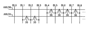
図8は上記抵抗相当素子の他の例を示す。図8では、図7においてプログラムセルPとしているアジャストセルAC01,AC02,AC04〜AC07のうち、放電されるメインビット線BL1〜BL3に接続されるアジャストセルAC01,AC02に相当する素子として、アジャステッド・ワード線AWL0Hに共通にゲートが接続されたトランジスタ35,35を用いている。一方、放電されないメインビット線BL4〜BL8に接続されるアジャストセルAC04〜AC07に相当する素子として、アジャステッド・ワード線AWL0Mに共通にゲートが接続されたトランジスタ36,36,…を用いている。ここで、放電されるメインビット線BL1〜BL3間は低抵抗の方が好ましいので、アジャステッド・ワード線AWL0Hには高い電圧を与える。一方、放電されないメインビット線BL4〜BL8間は高抵抗の方が好ましいので、アジャステッド・ワード線AWL0Mには低い電圧を与える。
【0054】
また、上記メモリセルMCは、上述のようなトリプルウェルの中に構成されて非対象な濃度を有する拡散領域n+と拡散領域n−を有するメモリセルに限定されるものではなく、通常のNOR型等のメモリセルであっても構わない。また、上記実施の形態においては、1ブロックm本のメインビット線BLのうち1本〜(m−2)本のメインビット線BLを放電することと、全充電メインビット線間を抵抗相当素子で接続することとの両方を実施している。しかしながら、この発明は、何れか一方のみを実施しても構わない。
【0055】
【発明の効果】
以上より明らかなように、仮想グランド方式による半導体記憶装置において、第1スイッチング素子によって、ビット線の夫々を充電電源に接続して上記ビット線を充電し、制御手段による制御の下に第2スイッチング素子によって、連続して配列されたm本のビット線毎に、1本以上且つ(m−2)本以下の所定本数の連続して配列されたビット線の夫々を接地ラインに接続して放電するので、放電ビット線と充電ビット線とに接続された不揮発性メモリセルをオンしてこのオンされた不揮発性メモリセルに接続された充電ビット線の電圧をセンスすれば、当該不揮発性メモリセルの保持データを読み出すことができる。その場合に、上記放電ビット線と充電ビット線とに接続された不揮発性メモリセルは1ブロックm個の不揮発性メモリセル中に必ず2個存在するので、同時に2個の不揮発性メモリセルの保持データを読み出すことができる。
【0056】
さらに、読み出し対象の不揮発性メモリセル(読み出しセル)に隣接する2個の不揮発性メモリセルに接続されている2本のビット線の電位は同じであり、上記読み出しセルは放電ビット線同士あるいは充電ビット線同士を対向させて位置しているので、当該読み出しセルに対する隣接不揮発性メモリセルからのリーク電流の影響を最小限に止めることができる。したがって、上記一度に読み出せる2個の不揮発性メモリセル間の間隔を狭くでき、上記1ブロックの不揮発性メモリセル数を8個にすることが可能となる。
【0057】
さらに、上記接地ラインに接続される互いに隣り合う2本のビット線間および上記接地ラインに接続されない互いに隣り合う2本のビット線間に、オン状態でリーク電流が発生するような閾値電圧を有する抵抗相当素子としての不揮発性メモリセルを設けたので、上記放電ビット線と充電ビット線とに接続された不揮発性メモリセルの保持データを読み出す際に、上記接地ラインに接続されない互いに隣り合う2本のビット線間の抵抗相当素子としての不揮発性メモリセルをオンすることによってリーク電流が発生し、センスされるビット線に流れ込む。したがって、上記読み出しセルに隣接した不揮発性メモリセルの閾値電圧(すなわち保持データ)の差異によるセンス電圧のばらつきを少なくできる。
【0058】
すなわち、この発明によれば、上記読み出しセルに対する隣接セルの影響を更に少なくでき、上記1ブロック8個の不揮発性メモリセルにおける同時に2個の不揮発性メモリセルの読み出しを何の支承もなく実現できる。
【0059】
さらに、上記接地ラインに接続される互いに隣り合う2本のビット線間を接続している上記抵抗相当素子としての不揮発性メモリセルを、不揮発性メモリセル駆動手段によって、上記ビット線と接地ラインとが接続される前にオンするので、上記接地ラインに接続される上記所定数のビット線間にリーク電流を発生させて、上記接地されるビット線における放電前の電位を配線抵抗に拘わらず略同一電位に揃えることができる。したがって、上記接地されるビット線が放電される際の放電時間を揃えることができる。
【0060】
また、本発明の半導体記憶装置における上記抵抗相当素子は、接地されない互いに隣り合う2本のビット線にソースとドレインとが接続されてゲートに第1の所定電圧が印加される第1トランジスタと、接地される互いに隣り合う2本のビット線にソースとドレインとが接続されてゲートに上記第1の所定電圧より高い第2の所定電圧が印加されて上記第1トランジスタよりも低いオン抵抗を呈する第2トランジスタとで構成されているので、上記第1,第2トランジスタによって、接地されるビット線間および接地されないビット線間にリーク電流を発生させることができる。その場合に、接地されるビット線間に接続される第2トランジスタのオン抵抗が小さくなっているために、上記接地されるビット線を速やかに放電できる。
【図面の簡単な説明】
【図1】この発明の半導体記憶装置における等価回路図である。
【図2】図1に示す半導体記憶装置の読み出し動作のタイミングチャートである。
【図3】センスメインビット線の電圧変化に対する隣接メモリセルの保持データの影響を示す図である。
【図4】従来の半導体記憶装置におけるセンスメインビット線の電圧変化に対する隣接メモリセルの保持データの影響を示す図である。
【図5】放電メインビット線と読み出しメモリセルとの関係を示す図である。
【図6】1ブロック8本のメインビット線に対して1,2,4〜6本のメインビット線を放電する場合における放電メインビット線と読み出しメモリセルとの関係を示す図である。
【図7】図1とは異なるアジャストセルACの構成を示す図である。
【図8】図1とは異なる抵抗相当素子の構成例を示す図である。
【図9】従来の半導体記憶装置における等価回路図である。
【図10】図9に示す半導体記憶装置におけるセンスメモリセルと隣接メモリセルとの保持データによる拡散ビット線の電位を示す図である。
【符号の説明】
21…サブビット線、
22〜28,30,35,36…トランジスタ、
WL…ワード線、 BL…メインビット線、
MC…メモリセル、 AWL…アジャステッド・ワード線、
AC…アジャストセル、 SA…センスアンプ。[0001]
BACKGROUND OF THE INVENTION
The present invention relates to a virtual ground type semiconductor memory device.
[0002]
[Prior art]
In recent years, the capacity of semiconductor memory devices has increased significantly, and devices with a small effective cell area such as a multi-value method and a virtual ground method have been put on the market one after another in order to cope with low costs. In particular, since the virtual ground method can realize a small cell area only by devising a circuit, a device having a smaller chip area than other methods can be developed even in the same process.
[0003]
However, in the virtual ground method, the drain and source of the memory cell transistors arranged adjacent to each other in two columns are commonly connected to the same virtual bit line, so that leakage current from adjacent cells cannot be ignored. . Therefore, in the devices that have been commercialized so far, (1) as disclosed in Japanese Patent Laid-Open No. 6-68683, reading is performed by 8 sensing operations every 8 bits to eliminate the influence of leakage current. Yes. Or (2) the threshold voltage of the transistors constituting the memory cell every 8 bits is made higher than the threshold voltages of the transistors constituting the other memory cells (corresponding to holding data “0”, “1”) Current is prevented.
[0004]
FIG. 9 shows one block of the memory cell array disclosed in Japanese Patent Laid-Open No. 6-68683. When reading data held in the
[0005]
In this state, the potential of the
[0006]
[Problems to be solved by the invention]
However, the conventional virtual ground type semiconductor memory device has the following problems. (1) In the case of the semiconductor memory device disclosed in Japanese Patent Application Laid-Open No. 6-68683, as described above, in order to read the data held in all the memory cells connected to one word line, eight senses are performed. Requires action. Therefore, there is a problem that reading of retained data takes time and high-speed reading cannot be performed.
[0007]
In the semiconductor memory device of (2) described above, in order to dispose the invalid memory cells composed of transistors having a threshold voltage higher than the threshold voltage of the transistors of normal memory cells every 8 bits, effective memory cells There is a problem that the area becomes large.
[0008]
SUMMARY OF THE INVENTION Accordingly, an object of the present invention is to provide a semiconductor memory device capable of reading all memory cells connected to one word line by eight blocks in one sense line with four sensing operations while minimizing interference from adjacent memory cells. It is to provide.
[0009]
[Means for Solving the Problems]
To achieve the above object, in a semiconductor memory device having a plurality of nonvolatile memory cells arranged in a matrix and bit lines and word lines connected to each nonvolatile memory cell and configured by a virtual ground system, A charging power source for charging the bit line; a first switching element for intermittently connecting each of the bit lines and the charging power source; a grounded ground line; the bit line and the ground line;IntermittentA second switching element and m continuously arranged( m is an integer value of 4 or more )One or more per bit line and (m−2 ) BookThe second switching element is controlled so as to intermittently connect each of the predetermined number of bit lines continuously arranged and the ground line.Second switching elementControl meansBetween two adjacent bit lines connected to the ground line. , and , While connecting two adjacent bit lines not connected to the ground line, , A nonvolatile memory cell as a resistance-equivalent element having a threshold voltage at which a leakage current is generated in an on state, and the second switching element is controlled by the second switching element control means, so that the bit line and the ground line are Before being connected , Nonvolatile memory cell driving means for turning on nonvolatile memory cells as all the resistance-equivalent elementsA semiconductor memory device comprising:
[0010]
According to the above configuration, each of the bit lines is connected to the charging power source for a predetermined time by the first switching element, and all the bit lines are charged. After that, each of the predetermined number of bit lines of one or more of the m bit lines continuously arranged and (m−2) or less and the ground line are connected to the second line. Connected by the switching element, the predetermined number of bit lines are discharged. Therefore, the nonvolatile memory cell connected to the discharge bit line and the charge bit line is turned on, and the voltage of the charge bit line connected to the turned-on nonvolatile memory cell is sensed, whereby the nonvolatile memory cell is sensed. The data held in the memory cell is read out. In that case, since there are two nonvolatile memory cells connected to the discharge bit line and the charge bit line, the data held in the two nonvolatile memory cells are read at a time.
[0011]
Furthermore, the potentials of the two bit lines connected to the two nonvolatile memory cells adjacent to the nonvolatile memory cell to be read are the same, and the two nonvolatile memory cells to be read are discharge bits. The lines or the charge bit lines are located opposite to each other. Therefore, the influence of the leakage current from the adjacent nonvolatile memory cell on the nonvolatile memory cell to be read is minimized.The
[0012]
furtherWhen the data held in the nonvolatile memory cell connected to the discharge bit line and the charge bit line is read, it is connected to two adjacent bit lines that are not connected to the ground line.TauntThe nonvolatile memory cell as the anti-equivalent element is turned on. Then, a leak current from all the charged bit lines flows into the sensed bit line through the nonvolatile memory cell as the turned ON resistance equivalent element. Thus, the variation in sense voltage due to the difference in data held in the non-volatile memory cells adjacent to the charge side of the non-volatile memory cell to be read is reduced.The
[0013]
furtherA nonvolatile memory cell as the resistance equivalent element connected to two adjacent bit lines connected to the ground line,Before the bit line and ground line are connectedWhen turned on, a leak current is generated between the predetermined number of bit lines connected to the ground line, and the potential of the grounded bit line is made substantially the same regardless of the wiring resistance.As a result, the discharge time when the grounded bit line is discharged is made uniform.
[0014]
The resistance-corresponding element includes a first transistor in which a source and a drain are connected to two adjacent bit lines not connected to the ground line, and a first predetermined voltage is applied to a gate; The source and drain are connected to two adjacent bit lines connected to the ground line, and a second predetermined voltage higher than the first predetermined voltage is applied to the gate.Presents lower on-resistance than the first transistor.A semiconductor memory device comprising the second transistor.
[0015]
According to the above configuration, the first predetermined voltage is applied to the gate of the first transistor, while the second predetermined voltage is applied to the gate of the second transistor. Then, the first and second transistors are turned on, and a leak current is generated between the bit lines connected to the ground line and between the bit lines not connected to the ground line. In that case, since the second predetermined voltage applied to the gate of the second transistor connected between the grounded bit lines is higher than the first predetermined voltage applied to the gate of the first transistor, it is turned on. When the bit line to be grounded has a low resistance and is connected to the ground line by the second switching element, the ground bit line is quickly discharged.
[0016]
DETAILED DESCRIPTION OF THE INVENTION
Hereinafter, the present invention will be described in detail with reference to the illustrated embodiments.
FIG. 1 is an equivalent circuit diagram of the semiconductor memory device of the present embodiment. The memory cell array is configured by arranging (n × m) memory cell transistors (field effect transistors having a floating gate) in a matrix. The control gates of memory cell transistors (hereinafter simply referred to as memory cells) MC00 to MC0m arranged in the first row are connected to the word line WL0. Similarly, the control gates of the memory cells MCn0 to MCnm arranged in the (n + 1) th row are connected to the word line WLn.
[0017]
The memory cell MC is configured in a triple well, and has a diffusion region n + and a diffusion region n− which are in contact with each other and have non-target concentrations. The virtual ground type sub-bit line 21 is configured with the diffusion region n + on one side and the diffusion region n− on the other side. Each sub-bit line 21 is connected to the source or drain of n memory cells MC arranged in the same column, and further connected to the source or drain of n memory cells MC arranged in an adjacent column. . The odd-numbered sub-bit lines 21 are connected to the odd-numbered main bit lines BL0, BL2,..., BLm-1 through
[0018]
The memory cell array is divided into a plurality of blocks every (n × 8), and each block has the same configuration. Hereinafter, one block from the main bit line BL0 to the main bit line BL7 will be described as a representative.
[0019]
The main bit lines BL1 to BL3 are grounded through
[0020]
In addition, a positive leakage current is generated between the adjacent main bit lines BL between the adjacent main bit lines BL, and charging is performed regardless of whether the adjacent memory cell of the read memory cell is in the erased state or the programmed state. A resistance-equivalent element for making the leak current value from the main bit line BL to the read memory cell substantially the same is connected. In the present embodiment, the resistance equivalent element is a nonvolatile memory cell (hereinafter referred to as an adjustment cell) formed of a field effect transistor having a floating gate having a control gate commonly connected to the adjusted word line AWL0. It is composed of AC00 to AC07. Further, the adjustment cells AC10 to AC17 having the control gates commonly connected to the adjusted word line AWL1, the adjustment cells AC20 to AC27 having the control gates commonly connected to the adjusted word line AWL2, and the adjusted words The adjustment cells AC30 to AC37 are connected to the control line common to the line AWL3.
[0021]
Among the adjustment cells AC00 to AC07, the adjustment cells AC00 to AC03 are configured such that the threshold voltage of the transistors constituting the adjustment cell is higher than the “H” level voltage of the adjustment signal awl0 supplied to the adjusted word line AWL0. The adjustment cells AC04 to AC07 are high erase cells (indicated by “E” in the figure), and the threshold voltage of the transistors constituting the adjustment cells is “H” of the adjustment signal awl0 supplied to the adjusted word line AWL0. A program cell (indicated by “P” in the figure) lower than the level voltage. Of the adjustment cells AC10 to AC17, the adjustment cells AC12 to AC15 are the erase cells E, and the adjustment cells AC10, AC11, AC16, and AC17 are the program cells P. Of the adjustment cells AC20 to AC27, the adjustment cells AC24 to AC27 are the erase cells E, and the adjustment cells AC20 to AC23 are the program cells P. Of the adjustment cells AC30 to AC37, the adjustment cells AC30, AC31, AC36, and AC37 are the erase cells E, and the adjustment cells AC32 to AC35 are the program cells P.
[0022]
The odd-numbered main bit lines BL0, BL2, BL4, BL6, BL8 are charged lines to which the charging voltage Vpre is applied via the
[0023]
As described in detail below, the semiconductor memory device having the memory cell array configured as described above reads data held in all the memory cells MC connected to one word line WL by four sensing operations. FIG. 2 is an operation timing chart of the semiconductor memory device. In the following, the operation of the semiconductor memory device in the present embodiment will be described with reference to FIG. 2, taking as an example the case of reading data held in the memory cells MC00 to MC07 in the main block connected to the word line WL0. First, the level of the word line WL0 connected to the selected memory cells MC00 to MC07 is set to “H”, the level of the select gate selection signal sg is set to “H”, and all the sub bit lines 21 are connected to the main bit line BL. Thus, the read operation is started.
[0024]
(a) First reading (reading of memory cells MC00 and MC03)
At time t0, the level of the charging signal φpre is set to “H”, and all the main bit lines BL are charged to a charging voltage Vpre (for example, 1 V). Also, the adjustment signal awl0 supplied to the adjusted word line AWL0 is raised.
[0025]
At time t1, the level of the charging signal φpre is returned to “L”. After that, at time t2, the level of the discharge signal dis0 is set to “H”, and the main bit lines BL1 to BL3 are discharged. Here, when the data held in the memory cell MC00 is “0 (for example, the threshold voltage of the transistor constituting the memory cell MC00 is lower than the“ H ”level (Vcc) of the word line WL0: a program cell)” The main bit line BL0 is discharged through the sub bit line 21, the memory cell MC00 and the main bit line BL1. Similarly, when the data held in the memory cell MC03 is “0”, the main bit line BL4 is discharged via the sub bit line 21, the memory cell MC03 and the main bit line BL3. On the other hand, when the data held in the memory cells MC00 and MC03 is “1” (for example, the threshold voltage of the transistor is higher than the “H” level (Vcc) of the word line WL0: erase cell) ” Lines BL0 and BL4 are not discharged.
[0026]
Therefore, the sense amplifiers SA0 and SA4 are driven at time t3. Then, the voltages of the main bit lines BL0 and BL4 are detected by the sense amplifiers SA0 and SA4. If the voltage drops, it is determined that the data held in the memory cell MC00 or the memory cell MC03 is “0”, and the voltage must drop. For example, the data held in the memory cell MC00 or the memory cell MC03 is determined to be “1”. At time t4, the adjustment signal awl0 is lowered, the level of the discharge signal dis0 is set to “L”, and the first reading is completed.
[0027]
In that case, of the main bit lines BL0 to BL8, the main bit lines BL1 to BL3 are discharged. By doing so, the potential of the main bit line BL2 adjacent to the main bit line BL3 on the discharge side connected to the read memory cell MC03 is made the same as that of the main bit line BL3, and the main on the charge side (sense side) connected to the read memory cell MC03. The potential of the main bit line BL5 adjacent to the bit line BL4 is made the same as that of the main bit line BL4. That is, the source potential and drain potential of each of the memory cells MC02 and MC04 adjacent to the read memory cell MC03 are made the same. The read memory cell MC03 and the read memory cell MC00 closest to the read memory cell MC03 can have the discharge sides facing each other, and the distance between the charge sides can be separated as much as possible. Therefore, the influence of the leakage current from the adjacent memory cells MC02 and MC04 on the read memory cell MC03 can be minimized. The same applies to the read memory cell MC00.
[0028]
Of the adjustment cells AC00 to AC07 activated by the adjustment signal awl0, the adjustment cells AC00 to AC03 connected to the main bit lines BL1 to BL3 discharged by the discharge signal dis0 are erase cells E, and the others The adjustment cells AC04 to AC07 are program cells P. As a result, when the data held in the read memory cell MC03 is read, leak current flows into the main bit line BL4 through the adjustment cells AC04 to AC07, which are the program cells P, and the memory cells MC04 to MC07 are all the erase cells. There is no variation in leakage current (in other words, variation in the voltage of the main bit line BL4) between the case where there is one and the case where any one is the program cell. That is, there is no variation in leakage current between when the data held in the memory cell adjacent to the read memory cell MC03 is “0” and “1”. The same applies to the read memory cell MC00.
[0029]
(b) Second reading (reading of memory cells MC02 and MC05)
At time t5, the level of the charge signal φpre is set to “H”, and all the main bit lines BL are charged to the charge voltage Vpre. In addition, an adjustment signal awl1 supplied to the adjusted word line AWL1 is raised.
[0030]
At time t6, the level of the charging signal φpre is returned to “L”. After that, at time t7, the level of the discharge signal dis1 is set to “H”, and the main bit lines BL3 to BL5 are discharged. At time t8, the sense amplifiers SA2 and SA6 are driven to detect the voltages of the main bit lines BL2 and BL6, and the data held in the memory cells MC02 and MC05 are determined. At time t9, the adjustment signal awl1 is lowered, the level of the discharge signal dis1 is set to “L”, and the second reading is completed.
[0031]
In this case, among the main bit lines BL0 to BL8, the main bit lines BL3 to BL5 are discharged. Therefore, the source potential and drain potential of the memory cells MC04 and MC06 adjacent to the read memory cell MC05 are the same. Further, the read memory cell MC05 and the read memory cell MC02 closest to the read memory cell MC05 face each other on the discharge side and are separated as much as possible from the charge side in this state. Therefore, the influence of the leakage current from the adjacent memory cells MC04 and MC06 on the read memory cell MC05 can be minimized. The same can be said for the read memory cell MC02.
[0032]
Of the adjustment cells AC10 to AC17 activated by the adjustment signal awl1, the adjustment cells AC12 to AC15 connected to the main bit lines BL3 to BL5 discharged by the discharge signal dis1 are erase cells E, and the others The adjustment cells AC10, AC11, AC16, and AC17 are program cells P. Therefore, when reading the data held in the read memory cell MC05, there is a variation in leakage current between when the memory cells MC01, MC01, MC06, and MC07 are all the erase cells and when any one is the program cell. It can be lost. The same can be said for the read memory cell MC02.
[0033]
(c) Third reading (reading of memory cells MC04 and MC07)
At time t10, the level of the charging signal φpre is set to “H”, and all the main bit lines BL are charged to the charging voltage Vpre. Also, the adjustment signal awl2 supplied to the adjusted word line AWL2 is raised.
[0034]
At time t11, the level of the charge signal φpre is returned to “L”. After that, at time t12, the level of the discharge signal dis2 is set to “H”, and the main bit lines BL5 to BL7 are discharged. At time t13, the sense amplifiers SA3 and SA7 are driven to detect the voltages of the main bit lines BL4 and BL8, and the data held in the memory cells MC04 and MC07 is determined. At time t14, the adjustment signal awl2 is lowered, the level of the discharge signal dis2 is set to “L”, and the third reading is completed.
[0035]
In that case, of the main bit lines BL0 to BL8, the main bit lines BL5 to BL7 are discharged. Therefore, the source potential and the drain potential of the memory cells MC03 and MC05 adjacent to the read memory cell MC04 are the same. Further, the read memory cell MC04 and the read memory cell MC07 closest to the read memory cell MC04 face each other on the discharge side and are separated as much as possible from the charge side in this state. Therefore, the influence of the leakage current from the adjacent memory cells MC03 and MC05 on the read memory cell MC04 can be minimized. The same is true for the read memory cell MC07.
[0036]
Of the adjustment cells AC20 to AC27 activated by the adjustment signal awl2, the adjustment cells AC24 to AC27 connected to the main bit lines BL5 to BL7 discharged by the discharge signal dis2 are the erase cells E. The adjustment cells AC20 to AC23 are program cells P. Therefore, when reading the data held in the read memory cell MC04, it is possible to eliminate variations in leakage current between when the memory cells MC00 to MC03 are all the erase cells and when any one is the program cell. . The same is true for the read memory cell MC07.
[0037]
(d) Fourth reading (reading of memory cells MC01 and MC06)
At time t15, the level of the charge signal φpre is set to “H”, and all the main bit lines BL are charged to the charge voltage Vpre. Also, the adjustment signal awl3 supplied to the adjusted word line AWL3 is raised.
[0038]
At time t16, the level of the charging signal φpre is returned to “L”. After that, at time t17, the level of the discharge signal dis3 is set to “H”, and the main bit lines BL0, BL1, BL7, BL8 are discharged. At time t18, the sense amplifiers SA1 and SA5 are driven to detect the voltages of the main bit lines BL2 and BL6, and the data held in the memory cells MC01 and MC06 are determined. At time t19, the level of the word line WL0 is lowered, the level of the select gate selection signal sg is set to "L", the adjustment signal awl3 is lowered, and the level of the discharge signal dis3 is set to "L". End the second reading.
[0039]
In this case, among the main bit lines BL0 to BL8, the main bit lines BL0, BL1, BL7, BL8 are discharged. Therefore, the source potential and the drain potential of the adjacent memory cells MC00 and MC02 of the read memory cell MC01 are the same. In addition, the read memory cell MC01 and the read memory cell MC06 closest to the read memory cell MC01 are arranged such that the charging sides face each other and the charging sides are separated as much as possible in this state. Therefore, the influence of the leakage current from the adjacent memory cells MC00 and MC02 on the read memory cell MC01 can be minimized. The same applies to the read memory cell MC06.
[0040]
Among the adjustment cells AC30 to AC37 activated by the adjustment signal awl3, the adjustment cells AC30, AC31, AC36, AC37 connected to the main bit lines BL0, BL1, BL7, BL8 discharged by the discharge signal dis3 are The erase cell E and the other adjust cells AC32 to AC35 are program cells P. Therefore, when reading the data held in the read memory cell MC01, it is possible to eliminate variations in leakage current between when the memory cells MC02 to MC05 are all the erase cells and when any one is the program cell. . The same applies to the read memory cell MC06.
[0041]
As described above, in this embodiment, the memory cells MC00 and MC03 are read at the first time, the memory cells MC02 and MC05 are read at the second time, the memory cells MC04 and MC07 are read at the third time, and the memory cell MC01 is read at the fourth time. , MC06 is read out, all the memory cells MC00 to MC07 in one block can be read out four times. By performing the same operation at the same time for all blocks, it is possible to read the data held in all the memory cells MC00 to MC0m connected to one word line WL0 by four sensing operations.
[0042]
In this case, after all the memory cells MC are once charged to the charging voltage Vpre, two main bit lines BL connected to one of the two memory cells MC read by one read operation and the other for one block. Of the two main bit lines BL connected to the two main bit lines BL located on the near side and all the main bit lines BL between the two main bit lines BL, or on the far side The two main bit lines BL positioned and all the main bit lines BL located outside the two main bit lines BL are discharged.
[0043]
Accordingly, the source potential and drain potential of each of the two memory cells MC adjacent to the read memory cell can be made the same. In addition, both read memory cells can have the discharge sides or the charge sides face each other, and in this state, the charge sides can be separated as much as possible. As a result, the influence of the leakage current from both adjacent memory cells on the read memory cell can be minimized. That is, the interval between memory cells to be read simultaneously can be reduced, and two memory cells MC can be simultaneously read from eight memory cells MC in one block without any trouble.
[0044]
Further, the adjustment cell AC connected to the discharged main bit line BL is the erase cell E, and the other adjustment cells AC are the program cells P. Therefore, when reading data held in the read memory cell, a leak current flows into the main bit line BL sensed by the sense amplifier SA through the adjustment cell AC (program cell P) connected to the charged main bit line BL. It will be. For this reason, variations in leakage current between the case where all the memory cells MC whose source / drain are connected to the charging main bit line are all the erase cells and the case where any one is the program cell are reduced.
[0045]
FIG. 3 shows a voltage change of the main bit line BL sensed by the sense amplifier SA during one read process. In the figure, “E” is a voltage change when the read memory cell is the erase cell, and “P” is a voltage change when the read memory cell is the program cell. Further, the suffix “1” of “E, P” indicates that the adjacent memory cell is the erased cell, and “2” indicates that the adjacent memory cell is the programmed cell. FIG. 4 is a diagram corresponding to FIG. 3 in a conventional semiconductor memory device that does not use the adjusted word line AWL and the adjustment cell AC.
[0046]
From FIG. 4, when the adjusted word line AWL and the adjustment cell AC are not used, the influence of the leakage current from the adjacent memory cell of the read memory cell on the sense main bit line is that the adjacent memory cell is the erase cell. And the case of the program cell. Therefore, in the case of a conventional semiconductor memory device, it is necessary to increase the interval between memory cells to be read simultaneously, and the number of memory cells that can be read simultaneously from eight memory cells in one block is limited to one. As a result, eight sense operations are required for reading from eight memory cells in one block.
[0047]
On the other hand, in the case of the semiconductor memory device in the present embodiment, a leakage current flows to the sensed main bit line BL through the adjustment cell AC (program cell P) connected to the charged main bit line BL. Flows in. Therefore, as shown in FIG. 3, the influence of the leakage current from the adjacent memory cell does not vary between the case where the adjacent memory cell is the erased cell and the case of the programmed cell, and the point A where both curves intersect Exists. Therefore, by setting the sense start time at this point A, the variation in the voltage of the sense main bit line due to the leakage current from the adjacent memory cell is reduced. Therefore, the interval between the memory cells to be read simultaneously can be reduced, and reading can be performed in four sensing operations for eight memory cells in one block.
[0048]
Incidentally, in the above embodiment in which three main bit lines BL are discharged with respect to eight main bit lines BL in one block, the relationship between the discharge main bit lines and the read memory cells is shown in FIG. It is like that. In FIG. 5, “0” indicates a discharge main bit line, and “1” indicates a charge main bit line. In addition, the read memory cell in that case is shown next to “0” and “1” indicating discharge / charge. As shown in FIG. 5, two memory cells MC in which either one of the source or the drain is connected to the discharge main bit line and the other is connected to the charge main bit line are used as read memory cells.
(A) The source potential and drain potential of each memory cell adjacent to the read memory cell are made the same.
(B) The read memory cell and the read memory cell closest to the read memory cell are placed with the discharge sides or the charge sides facing each other, and in this state, the distance between the charge sides is separated as much as possible.
Has realized.
[0049]
The two memory cells MC in which either one of the source or the drain is connected to the discharge main bit line and the other is connected to the charge main bit line are used as a read memory cell. This is not realized by discharging only three main bit lines BL at the time of one read operation for one main bit line BL. As shown in FIG. When discharging one main bit line BL with respect to BL, discharging two main bit lines BL, discharging four main bit lines BL, discharging five main bit lines BL In this case, it can also be realized when six main bit lines BL are discharged. In other words, for the m main bit lines BL per block, the main bit lines BL that are continuously arranged with “1” or more and “m−2 (number of read memory cells)” or less at the time of one read operation. This can be realized by discharging. In this case, it is necessary to change the position and the number of program cells P in the adjustment cell AC in accordance with the change in the position and the number of discharge main bit lines.
[0050]
The configuration of the adjustment cell AC is not limited to the configuration shown in FIG. FIG. 7 shows another configuration example of the adjustment cells AC00 to AC07 in FIG.
[0051]
In FIG. 7, only the adjustment cells AC00, AC03 connected to the same main bit lines BL0, BL1, BL3, BL4 as the read memory cells MC00, MC03 are the erase cells E, and the other adjustment cells AC01, AC02, AC04 to AC07. Is a program cell P. In this way, the adjustment cells AC01 and AC02 are set to the program cell P, so that the main bit lines BL1 to BL3 are discharged with the same potentials of the main bit lines BL1 to BL3 before discharge regardless of differences in wiring resistance. The discharge time can be made uniform.
[0052]
In the above embodiment, the adjusted equivalent element is used as the resistance equivalent element that makes the variation in leakage current from the adjacent memory cell to the read memory cell the same regardless of whether the adjacent memory cell is an erase cell or a program cell. A word line AWL and an adjustment cell AC that is a nonvolatile memory cell are used. However, the present invention is not limited to this, and any resistance-corresponding element that generates a leakage current as described above may be used. However, when a nonvolatile memory cell is used as the resistance-corresponding element, the same nonvolatile memory cell as the data holding nonvolatile memory cell MC can be used, and the area occupied by the resistance-corresponding element can be reduced.
[0053]
FIG. 8 shows another example of the resistance equivalent element. 8, the adjusted cells AC01, AC02, and AC04 to AC07 as the program cell P in FIG. 7 are adjusted as elements corresponding to the adjusted cells AC01 and AC02 connected to the discharged main bit lines BL1 to BL3. -
[0054]
In addition, the memory cell MC is not limited to a memory cell that is configured in the triple well as described above and has a diffusion region n + and a diffusion region n− having a non-target concentration. It may be a memory cell such as. In the above embodiment, one to (m−2) main bit lines BL out of m main bit lines BL in one block are discharged, and a resistance equivalent element is provided between all charged main bit lines. And both are connected with. However, this invention may be implemented only in either one.
[0055]
【The invention's effect】
As apparent from the above, in the semiconductor memory device using the virtual ground system, the first switching element connects each of the bit lines to the charging power source to charge the bit line, and the second switching is performed under the control of the control means. For every m bit lines arranged continuously by the element, each of a predetermined number of bit lines arranged at least 1 and not more than (m−2) is connected to the ground line and discharged. Therefore, if the nonvolatile memory cell connected to the discharge bit line and the charge bit line is turned on and the voltage of the charge bit line connected to the turned on nonvolatile memory cell is sensed, the nonvolatile memory cell Can be read. In that case, since there are necessarily two nonvolatile memory cells connected to the discharge bit line and the charge bit line in one block of m nonvolatile memory cells, two nonvolatile memory cells are held simultaneously. Data can be read out.
[0056]
Further, the potentials of the two bit lines connected to the two nonvolatile memory cells adjacent to the nonvolatile memory cell (read cell) to be read are the same, and the read cell is connected to the discharge bit lines or charged. Since the bit lines are opposed to each other, the influence of the leakage current from the adjacent nonvolatile memory cell on the read cell can be minimized. Therefore, the interval between the two non-volatile memory cells that can be read at a time can be narrowed, and the number of non-volatile memory cells in one block can be reduced to eight.The
[0057]
furtherThe two adjacent bit lines connected to the ground line and the two adjacent bit lines not connected to the ground lineIn between, it has a threshold voltage that causes leakage current in the on stateResistance equivalent elementNonvolatile memory cell asTherefore, when reading the data held in the nonvolatile memory cells connected to the discharge bit line and the charge bit line, between the two adjacent bit lines not connected to the ground lineofResistance equivalent elementBy turning on non-volatile memory cells asLeakage current is generatedAndFlows into the bit line to be sensed. Therefore, it is possible to reduce the variation in the sense voltage due to the difference in threshold voltage (that is, retained data) of the nonvolatile memory cell adjacent to the read cell.
[0058]
That is, according to the present invention, the influence of adjacent cells on the read cell can be further reduced, and reading of two non-volatile memory cells at the same time in the one block of eight non-volatile memory cells can be realized without any support.The
[0059]
furtherBetween two adjacent bit lines connected to the ground line.ConnectedNonvolatile memory cell as the resistance equivalent elementThe,Since the nonvolatile memory cell driving means is turned on before the bit line and the ground line are connected,The leaked current is generated between the predetermined number of bit lines connected to the ground line, and the grounded bit lineBefore discharge inCan be set to substantially the same potential regardless of the wiring resistance.Accordingly, the discharge time when the grounded bit line is discharged can be made uniform.
[0060]
In the semiconductor memory device of the present invention, the resistance-corresponding element includes a first transistor in which a source and a drain are connected to two adjacent bit lines that are not grounded and a first predetermined voltage is applied to a gate; A source and a drain are connected to two adjacent bit lines that are grounded, and a second predetermined voltage higher than the first predetermined voltage is applied to the gate.Presents lower on-resistance than the first transistor.Therefore, the first and second transistors can generate a leakage current between the grounded bit lines and between the ungrounded bit lines. In this case, since the on-resistance of the second transistor connected between the grounded bit lines is small, the grounded bit line can be discharged quickly.
[Brief description of the drawings]
FIG. 1 is an equivalent circuit diagram of a semiconductor memory device according to the present invention.
2 is a timing chart of a read operation of the semiconductor memory device shown in FIG.
FIG. 3 is a diagram showing the influence of data held in adjacent memory cells on a voltage change of a sense main bit line.
FIG. 4 is a diagram showing the influence of data held in adjacent memory cells on a voltage change of a sense main bit line in a conventional semiconductor memory device.
FIG. 5 is a diagram showing a relationship between a discharge main bit line and a read memory cell.
FIG. 6 is a diagram showing a relationship between a discharge main bit line and a read memory cell when discharging 1, 2, 4 to 6 main bit lines with respect to eight main bit lines in one block;
7 is a diagram showing a configuration of an adjustment cell AC different from FIG.
FIG. 8 is a diagram illustrating a configuration example of a resistance-equivalent element different from that in FIG.
FIG. 9 is an equivalent circuit diagram of a conventional semiconductor memory device.
10 is a diagram showing a potential of a diffusion bit line according to data held in a sense memory cell and an adjacent memory cell in the semiconductor memory device shown in FIG. 9;
[Explanation of symbols]
21 ... Sub-bit line,
22-28, 30, 35, 36 ... transistor,
WL ... word line, BL ... main bit line,
MC ... memory cell, AWL ... adjusted word line,
AC ... Adjust cell, SA ... Sense amplifier.
Claims (2)
上記ビット線を充電するための充電電源と、
上記ビット線の夫々と上記充電電源とを断続する第1スイッチング素子と、
接地された接地ラインと、
上記ビット線と接地ラインとを断続する第2スイッチング素子と、
連続して配列されたm( mは4以上の整数値 )本のビット線毎に、1本以上であり且つ(m−2 ) 本以下である所定本数の連続して配列されたビット線の夫々と上記接地ラインとを断続するように上記第2スイッチング素子を制御する第2スイッチング素子制御手段と、
上記接地ラインに接続される互いに隣り合う2本のビット線間、および、上記接地ラインに接続されない互いに隣り合う2本のビット線間を接続すると共に、オン状態でリーク電流が発生するような閾値電圧を有する抵抗相当素子としての不揮発性メモリセルと、
上記第2スイッチング素子制御手段によって上記第2スイッチング素子が制御されて上記ビット線と接地ラインとが接続される前に、総ての上記抵抗相当素子としての不揮発性メモリセルをオンにする不揮発性メモリセル駆動手段
を備えたことを特徴とする半導体記憶装置。In a semiconductor memory device having a plurality of nonvolatile memory cells arranged in a matrix and a bit line and a word line connected to each nonvolatile memory cell and configured by a virtual ground system,
A charging power source for charging the bit line;
A first switching element for intermittently connecting each of the bit lines and the charging power source;
A grounded ground line;
A second switching element for intermittently connecting the bit line and the ground line;
Are continuously arranged m (m is an integer of 4 or more values) for each of bit lines, not less than one and (m-2) of the consecutively arranged bit lines of a predetermined number or less present Second switching element control means for controlling the second switching element so as to intermittently connect the ground line with each other ;
A threshold that connects between two adjacent bit lines connected to the ground line and between two adjacent bit lines not connected to the ground line, and causes a leak current to be generated in an ON state. A nonvolatile memory cell as a resistance equivalent element having a voltage;
Non-volatile that turns on all non-volatile memory cells as the resistance-equivalent elements before the second switching element is controlled by the second switching element control means and the bit line and the ground line are connected. A semiconductor memory device comprising memory cell driving means .
上記ビット線を充電するための充電電源と、
上記ビット線の夫々と上記充電電源とを断続する第1スイッチング素子と、
接地された接地ラインと、
上記ビット線と接地ラインとを断続する第2スイッチング素子と、
連続して配列されたm ( mは4以上の整数値 ) 本のビット線毎に、1本以上であり且つ ( m−2 ) 本以下である所定本数の連続して配列されたビット線の夫々と上記接地ラインとを断続するように上記第2スイッチング素子を制御する第2スイッチング素子制御手段と、
上記接地ラインに接続されない互いに隣り合う2本のビット線にソースとドレインとが接続されると共に、第1の所定電圧がゲートに印加される第1トランジスタと、
上記接地ラインに接続される互いに隣り合う2本のビット線にソースとドレインとが接続されると共に、上記第1の所定電圧より高い第2の所定電圧がゲートに印加されて上記第1トランジスタよりも低いオン抵抗を呈する第2トランジスタ
を備えたことを特徴とする半導体記憶装置。In a semiconductor memory device having a plurality of nonvolatile memory cells arranged in a matrix and a bit line and a word line connected to each nonvolatile memory cell and configured by a virtual ground system,
A charging power source for charging the bit line;
A first switching element for intermittently connecting each of the bit lines and the charging power source;
A grounded ground line;
A second switching element for intermittently connecting the bit line and the ground line;
A predetermined number of consecutively arranged bit lines that are 1 or more and ( m−2 ) or less per m ( m is an integer value of 4 or more ) continuously arranged bit lines . Second switching element control means for controlling the second switching element so as to intermittently connect the ground line with each other ;
A first transistor in which a source and a drain are connected to two adjacent bit lines not connected to the ground line, and a first predetermined voltage is applied to a gate;
A source and a drain are connected to two adjacent bit lines connected to the ground line, and a second predetermined voltage higher than the first predetermined voltage is applied to the gate so that the first transistor A semiconductor memory device comprising: a second transistor exhibiting a low on-resistance .
Priority Applications (6)
| Application Number | Priority Date | Filing Date | Title |
|---|---|---|---|
| JP27427297A JP3608919B2 (en) | 1997-10-07 | 1997-10-07 | Semiconductor memory device |
| TW087114721A TW434554B (en) | 1997-10-07 | 1998-09-04 | A virtual ground type semiconductor storage device |
| US09/151,087 US6088265A (en) | 1997-10-07 | 1998-09-10 | Virtual ground type semiconductor storage device |
| EP98307448A EP0908896B1 (en) | 1997-10-07 | 1998-09-15 | A virtual ground type semiconductor storage device |
| DE69828932T DE69828932T2 (en) | 1997-10-07 | 1998-09-15 | Semiconductor storage device with virtual grounding |
| KR1019980039164A KR100283520B1 (en) | 1997-10-07 | 1998-09-22 | Virtual Grounding Semiconductor Storage Device |
Applications Claiming Priority (1)
| Application Number | Priority Date | Filing Date | Title |
|---|---|---|---|
| JP27427297A JP3608919B2 (en) | 1997-10-07 | 1997-10-07 | Semiconductor memory device |
Publications (2)
| Publication Number | Publication Date |
|---|---|
| JPH11110987A JPH11110987A (en) | 1999-04-23 |
| JP3608919B2 true JP3608919B2 (en) | 2005-01-12 |
Family
ID=17539356
Family Applications (1)
| Application Number | Title | Priority Date | Filing Date |
|---|---|---|---|
| JP27427297A Expired - Fee Related JP3608919B2 (en) | 1997-10-07 | 1997-10-07 | Semiconductor memory device |
Country Status (6)
| Country | Link |
|---|---|
| US (1) | US6088265A (en) |
| EP (1) | EP0908896B1 (en) |
| JP (1) | JP3608919B2 (en) |
| KR (1) | KR100283520B1 (en) |
| DE (1) | DE69828932T2 (en) |
| TW (1) | TW434554B (en) |
Families Citing this family (18)
| Publication number | Priority date | Publication date | Assignee | Title |
|---|---|---|---|---|
| JP3206591B2 (en) * | 1999-02-08 | 2001-09-10 | 日本電気株式会社 | Multi-value mask ROM and method of reading multi-value mask ROM |
| JP3709132B2 (en) * | 2000-09-20 | 2005-10-19 | シャープ株式会社 | Nonvolatile semiconductor memory device |
| KR100416599B1 (en) * | 2001-05-31 | 2004-02-05 | 삼성전자주식회사 | Memory cell structure of metal programmable ROM capable of improving memory density and read speed and reducing power consumption |
| JP4859294B2 (en) * | 2001-07-10 | 2012-01-25 | 富士通セミコンダクター株式会社 | Nonvolatile semiconductor memory device |
| JP4454896B2 (en) * | 2001-09-27 | 2010-04-21 | シャープ株式会社 | Virtual ground type nonvolatile semiconductor memory device |
| JP2003157689A (en) * | 2001-11-20 | 2003-05-30 | Hitachi Ltd | Semiconductor device and data processor |
| JP2003281896A (en) | 2002-03-22 | 2003-10-03 | Fujitsu Ltd | Semiconductor memory device |
| US6771543B2 (en) * | 2002-08-22 | 2004-08-03 | Advanced Micro Devices, Inc. | Precharging scheme for reading a memory cell |
| US7755938B2 (en) * | 2004-04-19 | 2010-07-13 | Saifun Semiconductors Ltd. | Method for reading a memory array with neighbor effect cancellation |
| US8116142B2 (en) * | 2005-09-06 | 2012-02-14 | Infineon Technologies Ag | Method and circuit for erasing a non-volatile memory cell |
| JP5028007B2 (en) * | 2005-12-01 | 2012-09-19 | ラピスセミコンダクタ株式会社 | Nonvolatile storage device and writing method thereof |
| US7429894B2 (en) | 2005-12-08 | 2008-09-30 | Electronics And Telecommunications Research Institute | Power device having connection structure compensating for reactance component of transmission line |
| US7692960B2 (en) * | 2006-12-20 | 2010-04-06 | Macronix International Co., Ltd. | Scheme of semiconductor memory and method for operating same |
| US7965551B2 (en) * | 2007-02-07 | 2011-06-21 | Macronix International Co., Ltd. | Method for metal bit line arrangement |
| KR101489392B1 (en) * | 2009-02-02 | 2015-02-03 | 삼성전자주식회사 | Read operation method of memory device |
| JP6306233B1 (en) | 2017-02-28 | 2018-04-04 | ウィンボンド エレクトロニクス コーポレーション | Flash memory and manufacturing method thereof |
| JP6563988B2 (en) | 2017-08-24 | 2019-08-21 | ウィンボンド エレクトロニクス コーポレーション | Nonvolatile semiconductor memory device |
| JP6623247B2 (en) | 2018-04-09 | 2019-12-18 | ウィンボンド エレクトロニクス コーポレーション | Flash memory and manufacturing method thereof |
Family Cites Families (7)
| Publication number | Priority date | Publication date | Assignee | Title |
|---|---|---|---|---|
| US5027321A (en) * | 1989-11-21 | 1991-06-25 | Intel Corporation | Apparatus and method for improved reading/programming of virtual ground EPROM arrays |
| JP2863661B2 (en) * | 1991-12-16 | 1999-03-03 | 株式会社東芝 | Read-only memory |
| JP3295137B2 (en) * | 1992-08-21 | 2002-06-24 | 株式会社リコー | Memory device and reading method thereof |
| JP2565104B2 (en) * | 1993-08-13 | 1996-12-18 | 日本電気株式会社 | Virtual ground type semiconductor memory device |
| US5517448A (en) * | 1994-09-09 | 1996-05-14 | United Microelectronics Corp. | Bias circuit for virtual ground non-volatile memory array with bank selector |
| JP2643896B2 (en) * | 1995-02-23 | 1997-08-20 | 日本電気株式会社 | Semiconductor memory |
| JP2882370B2 (en) * | 1996-06-28 | 1999-04-12 | 日本電気株式会社 | Semiconductor storage device |
-
1997
- 1997-10-07 JP JP27427297A patent/JP3608919B2/en not_active Expired - Fee Related
-
1998
- 1998-09-04 TW TW087114721A patent/TW434554B/en not_active IP Right Cessation
- 1998-09-10 US US09/151,087 patent/US6088265A/en not_active Expired - Fee Related
- 1998-09-15 EP EP98307448A patent/EP0908896B1/en not_active Expired - Lifetime
- 1998-09-15 DE DE69828932T patent/DE69828932T2/en not_active Expired - Fee Related
- 1998-09-22 KR KR1019980039164A patent/KR100283520B1/en not_active IP Right Cessation
Also Published As
| Publication number | Publication date |
|---|---|
| KR100283520B1 (en) | 2001-03-02 |
| KR19990036660A (en) | 1999-05-25 |
| JPH11110987A (en) | 1999-04-23 |
| TW434554B (en) | 2001-05-16 |
| DE69828932T2 (en) | 2006-03-30 |
| EP0908896B1 (en) | 2005-02-09 |
| EP0908896A3 (en) | 2000-03-29 |
| EP0908896A2 (en) | 1999-04-14 |
| DE69828932D1 (en) | 2005-03-17 |
| US6088265A (en) | 2000-07-11 |
Similar Documents
| Publication | Publication Date | Title |
|---|---|---|
| JP3608919B2 (en) | Semiconductor memory device | |
| US5732018A (en) | Self-contained reprogramming nonvolatile integrated circuit memory devices and methods | |
| KR930000869B1 (en) | Flash type eeprom device which is able to eliminate page | |
| KR100897590B1 (en) | Dual-cell soft programming for virtual-ground memory arrays | |
| US6317349B1 (en) | Non-volatile content addressable memory | |
| US5313432A (en) | Segmented, multiple-decoder memory array and method for programming a memory array | |
| KR100284916B1 (en) | Semiconductor memory device and its write control method | |
| US6654290B2 (en) | Flash memory device with cell current measuring scheme using write driver | |
| US5687117A (en) | Segmented non-volatile memory array with multiple sources having improved source line decode circuitry | |
| KR100559716B1 (en) | NAND flash memory device and method of reading the same | |
| KR100280023B1 (en) | Nonvolatile Semiconductor Memory with Background Operation Mode | |
| US7196943B2 (en) | Memory device | |
| KR100648121B1 (en) | Nonvolatile semiconductor memory device and controlling method thereof | |
| KR100491912B1 (en) | Nonvolatile semiconductor memory | |
| KR970051349A (en) | Threshold Voltage Rising Method for Nonvolatile Semiconductor Memory and Exhausted Memory Cells | |
| KR100297669B1 (en) | Semiconductor storage, with the ability to perform sweeping pie-fire operations in aggregate for all memory cells | |
| JP2003272395A (en) | Nonvolatile semiconductor memory device | |
| JP3574322B2 (en) | Redundancy method for nonvolatile semiconductor memory | |
| KR20030019854A (en) | Nonvolatile semiconductor memory device that can suppress effect of threshold voltage variation of memory cell transistor | |
| EP0713223B1 (en) | Bit line sensing in a memory array | |
| JPH03288399A (en) | Semiconductor storage device | |
| JPH09180483A (en) | Semiconductor nonvolatile memory device | |
| KR970029851A (en) | Multi-State Nonvolatile Semiconductor Memory and Driving Method thereof | |
| KR100725093B1 (en) | semiconductor memory device having NOR type flat cell and driving method therefore | |
| KR100259973B1 (en) | Nor type mask rom |
Legal Events
| Date | Code | Title | Description |
|---|---|---|---|
| A977 | Report on retrieval |
Free format text: JAPANESE INTERMEDIATE CODE: A971007 Effective date: 20040310 |
|
| A131 | Notification of reasons for refusal |
Free format text: JAPANESE INTERMEDIATE CODE: A131 Effective date: 20040420 |
|
| A521 | Request for written amendment filed |
Free format text: JAPANESE INTERMEDIATE CODE: A523 Effective date: 20040616 |
|
| TRDD | Decision of grant or rejection written | ||
| A01 | Written decision to grant a patent or to grant a registration (utility model) |
Free format text: JAPANESE INTERMEDIATE CODE: A01 Effective date: 20041005 |
|
| A61 | First payment of annual fees (during grant procedure) |
Free format text: JAPANESE INTERMEDIATE CODE: A61 Effective date: 20041012 |
|
| R150 | Certificate of patent or registration of utility model |
Free format text: JAPANESE INTERMEDIATE CODE: R150 |
|
| FPAY | Renewal fee payment (event date is renewal date of database) |
Free format text: PAYMENT UNTIL: 20071022 Year of fee payment: 3 |
|
| FPAY | Renewal fee payment (event date is renewal date of database) |
Free format text: PAYMENT UNTIL: 20081022 Year of fee payment: 4 |
|
| FPAY | Renewal fee payment (event date is renewal date of database) |
Free format text: PAYMENT UNTIL: 20081022 Year of fee payment: 4 |
|
| FPAY | Renewal fee payment (event date is renewal date of database) |
Free format text: PAYMENT UNTIL: 20091022 Year of fee payment: 5 |
|
| FPAY | Renewal fee payment (event date is renewal date of database) |
Free format text: PAYMENT UNTIL: 20091022 Year of fee payment: 5 |
|
| FPAY | Renewal fee payment (event date is renewal date of database) |
Free format text: PAYMENT UNTIL: 20101022 Year of fee payment: 6 |
|
| FPAY | Renewal fee payment (event date is renewal date of database) |
Free format text: PAYMENT UNTIL: 20111022 Year of fee payment: 7 |
|
| FPAY | Renewal fee payment (event date is renewal date of database) |
Free format text: PAYMENT UNTIL: 20121022 Year of fee payment: 8 |
|
| FPAY | Renewal fee payment (event date is renewal date of database) |
Free format text: PAYMENT UNTIL: 20131022 Year of fee payment: 9 |
|
| LAPS | Cancellation because of no payment of annual fees |