JP3607571B2 - Print head drive circuit - Google Patents
Print head drive circuit Download PDFInfo
- Publication number
- JP3607571B2 JP3607571B2 JP2000149640A JP2000149640A JP3607571B2 JP 3607571 B2 JP3607571 B2 JP 3607571B2 JP 2000149640 A JP2000149640 A JP 2000149640A JP 2000149640 A JP2000149640 A JP 2000149640A JP 3607571 B2 JP3607571 B2 JP 3607571B2
- Authority
- JP
- Japan
- Prior art keywords
- transistor
- drive signal
- switching element
- turned
- exciting coil
- Prior art date
- Legal status (The legal status is an assumption and is not a legal conclusion. Google has not performed a legal analysis and makes no representation as to the accuracy of the status listed.)
- Expired - Lifetime
Links
Images


Description
【0001】
【発明の属する技術分野】
本発明は、ドットインパクトプリンタにおけるプリントヘッドの励磁コイルをを駆動するためのプリントヘッド駆動回路に関する。
【0002】
【従来の技術】
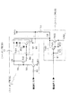
図7は従来技術の前提となる基本的なプリントヘッド駆動回路を示し、図7[1]は回路図、図7[2]は波形図である。以下、これらの図面に基づき説明する。
【0003】
図7[1]に示すように、基本的なプリントヘッド駆動回路は、励磁コイルL1の一端(以下「コモン側」という。)を電源電圧VDDに接続し、励磁コイルL1の他端(以下「シンク側」という。)をNPN型のトランジスタTrに接続したものである。
【0004】
トランジスタTrをONすると、電源電圧VDD→励磁コイルL1→トランジスタTr→GNDの順で電流が流れる。この電流は、図7[2]に示すように、励磁コイルL1の抵抗及びインダクタンスの時定数で上昇する。続いて、トランジスタTrをOFFすると、励磁コイルL1には電流を流し続けようとして逆起電力が生じる。この時、励磁コイルL1に蓄えられたエネルギーが原因で、シンク側には通常100V以上の非常に高い電圧(フライバック電圧)が発生する。
【0005】
このままでは、トランジスタTrが破損してしまうため、このエネルギーを逃がす必要がある。そこで、図7[1]に示すように、トランジスタTrのコレクタ−ベース間にツェナーダイオードZDを設けている。トランジスタTrがOFFした時に、ツェナーダイオードZDのツェナー電圧よりもフライバック電圧が高くなると、トランジスタTrのベースに電圧が加わることにより、トランジスタTrがONして電流を流す。そして、この電流が流れることにより、フライバック電圧がツェナー電圧よりも低くなると、トランジスタTrがOFFする。つまり、図7[2]に示すように、フライバックエネルギーをGNDに逃がすことによって、励磁コイルL1に流れる電流が急速に減少する。
【0006】
このようにして、プリントヘッドの励磁コイルL1に電流を流すことで、励磁コイルL1に電磁石力が生じるので、プリントヘッドのピンを駆動することができる。ピンの駆動方法には、バネ力に抗して電磁石力でピンをとばす方法(クラッパ式)や、電磁石力で永久磁石力をキャンセルしてバネ力でピンを飛ばす方法(スプリングチャージ式)等がある。
【0007】
ところで、高性能を追求すると、プリントヘッドには、一旦飛び出したピンをしばらく出したままにする、戻ってくる力を弱めてオーバーシュートを抑えるなどの動作が求められる。図8は、このような高性能化した従来のプリントヘッド駆動回路を示す回路図である。図2は、図8のプリントヘッド駆動回路の動作を示す波形図である。以下、これらの図面に基づき説明する。
【0008】
図8に示すように、従来のプリントヘッド駆動回路は、励磁コイルL1のコモン側にPNP型のトランジスタTr11を接続し、シンク側にNPN型のトランジスタTr12を接続し、トランジスタTr11を駆動信号S1で制御し、トランジスタTr12を駆動信号S2で制御するものである。駆動信号S2は、駆動信号S1と同時にオンになり、駆動信号S1よりも遅くオフになる。
【0009】
駆動信号S1は、ピンを飛び出させるため、及びピンを加速して高いインパクト力を付けるための信号である。駆動信号S2は、一旦飛び出したピンをできるだけそのまま保持するための信号である。駆動信号S2によって使われるエネルギーは、飛び出させる時のような大きさを必要としないので、電源電圧VDDから電流を供給せずに励磁コイルL1に蓄えられたエネルギーを利用する。
【0010】
図2に示す期間T1は、トランジスタTr11,Tr12,Tr13がすべてONする。この時の電流I1は、電源電圧VDD→トランジスタTr11→励磁コイルL1→トランジスタTr12→GNDの経路を流れる。
【0011】
期間T2は、トランジスタTr13がOFFすることによりトランジスタTr11がOFFし、トランジスタTr12がONのままである。この時の電流I2は、励磁コイルL1が電流を流し続けようとするので、GND→ダイオードD11→励磁コイルL1→トランジスタTr12→GNDの経路で流れる。
【0012】
期間T3は、トランジスタTr11がOFFし、トランジスタTr12もOFFした状態である。この時、励磁コイルL1には電流を流し続けようとして逆起電力が生じる。そのため、図8に示すA点には、励磁コイルL1に蓄えられたエネルギーに起因して非常に高い電圧が生じる。このままではトランジスタTr12が破損してしまうので、このフライバックエネルギーをダイオードD12及びツェナーダイオードZD11を通して電源電圧VDDに逃がす。これにより、(電源電圧)+(ツェナー電圧)で励磁コイルL1の端子電圧をクランプできるので、これ以上励磁コイルL1の端子電圧が上昇することはない。(電源電圧)+(ツェナー電圧)が大きいほど、短時間でフライバックエネルギーを吸収することができる。また、エネルギーを電源電圧VDDに逃がすことによって省エネルギーになる。よって、期間T3における電流I3は、GND→ダイオードD11→励磁コイルL1→ダイオードD12→ツェナーダイオードZD11→電源電圧VDDの経路を流れる。
【0013】
【発明が解決しようとする課題】
しかしながら、従来のプリントヘッド駆動回路には、次のような問題があった。
【0014】
(1).コモン側のトランジスタTr11、励磁コイルL1及びシンク側のトランジスタTr12が、電源に対して直列に接続されている。そのため、トランジスタ二個分のVce(sat)の電圧降下が生じるので、励磁コイルL1に印加される電圧が電源電圧VDDからかなり低いものになっていた。
【0015】
(2).図2に示すように、期間T1ではコモン側及びシンク側の両方のトランジスタTr11,Tr12に電流が流れ、期間T2ではシンク側のトランジスタTr12に電流が流れるため、トランジスタでの発熱量が多かった。
【0016】
(3).逆起電力によって励磁コイルL1に蓄えられたエネルギーを電源電圧VDDに逃がす方法では、全フライバックエネルギーをツェナーダイオードZD11で消費するので、ワット数が大きいツェナーダイオードZD11を必要とする。実際には、図8に示すように、ワット数の小さいものを数個直列に接続して発熱を分散させていた。そのため、部品点数が多くなり、プリント基板面積も大きくする必要があった。
【0017】
【発明の目的】
そこで、本発明の主な目的は、励磁コイルに印加される電圧を増加でき、トランジスタでの発熱量を減少でき、ツェナーダイオードを小容量にできる、プリントヘッド駆動回路を提供することにある。
【0018】
【課題を解決するための手段】
本発明に係るプリントヘッド駆動回路は、第一の駆動信号と、この第一の駆動信号と同時にオンになり第一の駆動信号よりも遅くオフになる第二の駆動信号とを用い、プリントヘッドの励磁コイルに電流を供給するものである。そして、励磁コイルと第一のスイッチング素子部とが電源に直列に接続され、第二及び第三のスイッチング素子部が励磁コイルにそれぞれ並列に接続されている。第一のスイッチング素子部は、第一の駆動信号のオンによって閉となることにより電源から励磁コイルに電流を供給し、第一の駆動信号のオフによって開となることにより励磁コイルからフライバック電流を発生させる。第二のスイッチング素子部は、第二の駆動信号のオンによって閉、第二の駆動信号のオフによって開となり、第二の駆動信号がオンかつ第一の駆動信号がオフの時にフライバック電流を励磁コイルに供給する。第三のスイッチング素子部は、第一及び第二の駆動信号がオフの時に、一定電圧以上印加されると閉となってフライバック電流を励磁コイルに供給する。なお、スイッチング素子部の「開閉」とは、言うまでもないが、スイッチの「開閉」と同義である。
【0019】
従来は、電源に対して「スイッチング素子部−励磁コイル−スイッチング素子部」と直列に接続されていた。そのため、二個のスイッチング素子部の電圧降下分を電源電圧から差し引いた電圧が、励磁コイルに印加されていた。これに対し、本発明では、電源に対して「励磁コイル−スイッチング部」と直列に接続されている。したがって、励磁コイルに印加される電圧は、一個のスイッチング素子部の電圧降下分だけを電源電圧から差し引いた電圧となるので、一個のスイッチング素子部の電圧降下分だけ従来よりも増加できる。
【0020】
また、従来は、第一の駆動信号がオンの時に、二個のスイッチング素子部に電流が流れていた。これに対し、本発明では、第一の駆動信号がオンの時に、一個のスイッチング素子部にだけ電流が流れるので、従来に比べてスイッチング素子部での発熱量を抑えることができる。
【0021】
更に、本発明は、次のような構成としてもよい。
【0022】
第一の駆動信号のみがチョッパ制御されたものである(請求項4)。第一のスイッチング素子部は、コレクタが励磁コイルのシンク側に接続されエミッタが接地されベースに第一の駆動信号が印加されるNPN型の第一のトランジスタを備える(請求項5)。第二のスイッチング素子部は、エミッタが接地されベースに第二の駆動信号が印加されるNPN型の第二のトランジスタと、ベースが第二のトランジスタのコレクタに接続されエミッタが励磁コイルのシンク側に接続されたPNP型の第三のトランジスタと、ベースが第三のトランジスタのコレクタに接続されエミッタが励磁コイルのコモン側に接続されたNPN型の第四のトランジスタと、アノードが励磁コイルのシンク側に接続されカソードが第四のトランジスタのコレクタに接続された第一のダイオードとを備える(請求項1)。第三のスイッチング素子部は、アノードが励磁コイルのシンク側に接続された第二のダイオードと、コレクタが第二のダイオードのカソードに接続されエミッタが励磁コイルのコモン側に接続されたNPN型の第五のトランジスタと、アノードが第五のトランジスタのベースに接続されカソードが第五のトランジスタのコレクタに接続されたツェナーダイオードとを備える(請求項2)。第二のスイッチング素子部は、エミッタが接地されベースに第二の駆動信号が印加されるNPN型の第二のトランジスタと、ベースが第二のトランジスタのコレクタに接続されエミッタが励磁コイルのシンク側に接続されたPNP型の第三のトランジスタと、ベースが第三のトランジスタのコレクタに接続されエミッタが励磁コイルのコモン側に接続されたNPN型の第四のトランジスタと、アノードが励磁コイルのシンク側に接続されカソードが第四のトランジスタのコレクタに接続された第一のダイオードとを備え、第三のスイッチング素子部は、アノードが励磁コイルのシンク側に接続された第一のダイオードと、コレクタがダイオードのカソードに接続されエミッタが励磁コイルのコモン側に接続された第四のトランジスタと、アノードが第四のトランジスタのベースに接続されカソードが第四のトランジスタのコレクタに接続されたツェナーダイオードとを備える(請求項3)。
【0023】
換言すると、本発明に係るプリントヘッド駆動回路は、電流のピーク値を抑える定電流チョッパ制御、又は電源からの電流供給なしに励磁コイルのインダクタに蓄えられたエネルギーにて励磁コイルにループ電流を流す制御、をする駆動回路において、励磁コイルの一端を電源に直接接続しながらも励磁コイルのフライバック起電力を利用して前記制御を可能とする励磁コイルのループ回路を持つことを特徴とする。
【0024】
【発明の実施の形態】
図1は、本発明に係るプリントヘッド駆動回路の第一実施形態を示す回路図である。図2は、図1のプリンタヘッド駆動回路の動作を示す波形図である。以下、これらの図面に基づき説明する。
【0025】
本実施形態のプリントヘッド駆動回路は、駆動信号S1と、駆動信号S1と同時にオンになり駆動信号S1よりも遅くオフになる駆動信号S2とを用い、プリントヘッドの励磁コイルL1に電流を供給するものである。そして、励磁コイルL1とスイッチング素子部10とが電源電圧VDDに直列に接続され、スイッチング素子部20,30が励磁コイルL1にそれぞれ並列に接続されている。スイッチング素子部10は、駆動信号S1のオンによって閉となることにより電源電圧VDDから励磁コイルL1に電流I1を供給し、駆動信号S1のオフによって開となることにより励磁コイルL1からフライバック電流I2,I3を発生させる。スイッチング素子部20は、駆動信号S2のオンによって閉、駆動信号S2のオフによって開となり、駆動信号S2がオンかつ駆動信号S1がオフの時にフライバック電流I2を励磁コイルL1に供給する。スイッチング素子部30は、駆動信号S1,S2がオフの時に、一定電圧以上印加されると閉となってフライバック電流I3を励磁コイルL1に供給する。
【0026】
スイッチング素子部10は、コレクタが励磁コイルL1のシンク側に接続されエミッタが接地されベースに駆動信号S1が印加されるNPN型のトランジスタTr2と、トランジスタTr2のベースに挿入された電流制限用の抵抗器R1とからなる。
【0027】
スイッチング素子部20は、エミッタが接地されベースに駆動信号S2が印加されるNPN型のトランジスタTr4と、トランジスタTr4のベースに挿入された電流制限用の抵抗器R2と、ベースがトランジスタTr4のコレクタに接続されエミッタがシンク側に接続されたPNP型のトランジスタTr3と、トランジスタTr4のコレクタとトランジスタTr3のベースとの間に挿入された電流制限用の抵抗器R3と、ベースがトランジスタTr3のコレクタに接続されエミッタがコモン側に接続されたNPN型のトランジスタTr1と、トランジスタTr3のコレクタとトランジスタTr1のベースとの間に挿入された電流制限用の抵抗器R4と、アノードがシンク側に接続されカソードがトランジスタTr1のコレクタに接続されたダイオードD1とからなる。
【0028】
スイッチング素子部30は、アノードがシンク側に接続されたダイオードD1と、コレクタがダイオードD1のカソードに接続されエミッタがコモン側に接続されたNPN型のトランジスタTr1と、アノードがトランジスタTr1のベースに接続されカソードがトランジスタTr1のコレクタに接続されたツェナーダイオードZD1とからなる。つまり、ダイオードD1及びトランジスタTr1は、スイッチング素子部20,30で共用されている。
【0029】
次に、本実施形態のプリンタヘッド駆動回路の動作を説明する。
【0030】
図2に示す期間T1では、シンク側のトランジスタTr2がONする。このとき、コモン側では、トランジスタTr3,Tr4がONしているものの、B点における電圧は0V近くとなる。そのため、トランジスタTr3に電流が流れないことにより、トランジスタTr1のベースに電圧が加わらないので、トランジスタTr1はONしない。すなわち、期間T1における電流I1は、電源電圧VDD→励磁コイルL1→トランジスタTr2→GNDの経路を流れる。したがって、この回路構成であれば、励磁コイルL1には電源電圧VDDを直接印加することができる。
【0031】
期間T2では、シンク側のトランジスタTr2がOFFする。このとき、励磁コイルL1には電流を流し続けようとして逆起電力が発生し、B点には非常に高いフライバック電圧が発生する。コモン側では、このフライバック電圧によってトランジスタTr3に電流が流れ、これによりトランジスタTr1のベースに電圧が加わるのでトランジスタTr1がONする。すなわち、期間T2における電流I2は、電源電圧VDD→励磁コイルL1→ダイオードD1→トランジスタTr1→励磁コイルL1→ダイオードD1のループ回路を流れる。
【0032】
期間T3では、トランジスタTr3,Tr1がOFFする。このとき、フライバック電圧が発生し、この電圧がツェナーダイオードZD1のツェナー電圧より高くなった場合に、トランジスタTr1のベースに電圧が加わるので、トランジスタTr1がONする。この時の電流は、トランジスタTr1を流れ、全フライバックエネルギーは(トランジスタTr1)+(ダイオードD1)+(励磁コイルL1)で消費される。すなわち、期間T3における電流I3は、励磁コイルL1→ダイオードD1→トランジスタTr1→励磁コイルL1の経路を流れる。なお、トランジスタTr1に電流が流れる時間は、(T2+T3)の期間だけであるため、図8の従来技術におけるトランジスタT12に比べて短い。
【0033】
以上説明したとおり、本実施形態のプリントヘッド駆動回路によれば、コモン側に電源電圧VDDを直結したままでも、図8の従来技術と同じように図2に示す電流を励磁コイルL1に流すことができる。また、シンク側のトランジスタTr2は、駆動信号S1がONの時(期間T1)のみ電流が流れ発熱する。その時、コモン側のトランジスタTr1は、電流が流れないので、発熱もしなければ、損失もない。そのため、トランジスタTr1は、図8の従来技術におけるトランジスタT12に比べて、ワット数の小さな安価なものを使用することができる。
【0034】
図3は、本発明に係るプリントヘッド駆動回路の第二実施形態を示す波形図である。以下、図1及び図3に基づき説明する。
【0035】
本実施形態では、第一実施形態における駆動信号S1を、図3に示すようなチョッパ制御した駆動信号S1としたものである。図1のプリントヘッド駆動回路は、このチョッパ制御された駆動信号S1を入力した場合でも問題なく動作する。また、チョッパ制御を実施した場合でも、従来技術に比べて、トランジスタに流れる電流の時間は各段に短いので、トランジスタの発熱を少なくすることができる。
【0036】
図4は、本発明に係るプリントヘッド駆動回路の第三実施形態を示す回路図である。以下、この図面に基づき説明する。ただし、図1と同じ部分は同じ符号を付すことにより説明を省略する。
【0037】
本実施形態のプリントヘッド駆動回路は、励磁コイルL1とスイッチング素子部11とが電源電圧VDDに直列に接続され、スイッチング素子部21,31が励磁コイルL1にそれぞれ並列に接続されている。スイッチング素子部11は、駆動信号S1のオンによって閉となることにより電源電圧VDDから励磁コイルL1に電流I1を供給し、駆動信号S1のオフによって開となることにより励磁コイルL1からフライバック電流I2,I3を発生させる。スイッチング素子部21は、駆動信号S2のオンによって閉、駆動信号S2のオフによって開となり、駆動信号S2がオンかつ駆動信号S1がオフの時にフライバック電流I2を励磁コイルL1に供給する。スイッチング素子部31は、駆動信号S1,S2がオフの時に、一定電圧以上印加されると閉となってフライバック電流I3を励磁コイルL1に供給する。
【0038】
コモン側のトランジスタTr10には、ワット数が小さくツェナーダイオードZD1を内蔵したNPN型を用いる。シンク側のトランジスタTr20には、NPN型として動作するダーリントントランジスタを用いる。トランジスタTr20は、駆動段のNPN型のトランジスタTr21と、パワー段のNPN型のトランジスタTr22と、トランジスタTr21のベース−エミッタ間の抵抗器R21と、トランジスタTr22のベース−エミッタ間の抵抗器R22とからなる。また、トランジスタTr3のベース−エミッタ間には抵抗器R5、トランジスタTr1のベース−エミッタ間には抵抗器R6がそれぞれ挿入されている。
【0039】
次に、図3及び図4に基づき、本実施形態のプリントヘッド駆動回路の動作を説明する。本実施形態では、図2の駆動信号でももちろん動作するが、図3の駆動信号を使うものとする。
【0040】
図3において、駆動信号S1,S2がともにONしている区間は、プリントヘッドのピンを前方に飛び出させる初動エネルギーを印加している。駆動信号S1がON/OFFを繰り返すチョッパ区間は、必要以上のエネルギー印加を抑制する。駆動信号S2のみONしている区間は、プリントヘッドのピンを継続して飛び出させる又は、プリントヘッドのピンの戻りを緩やかにする。
【0041】
駆動信号S1がONしている期間すなわち期間T1からチョッパOFF時間を除いた期間は、シンク側のトランジスタTr20がONしている。このとき、コモン側のトランジスタTr3,Tr4はONしているものの、C点における電圧は0V近くとなる。よって、トランジスタTr1のベースに電圧が加わらないため、トランジスタTr1には電流は流れない。すなわち、期間T1における電流I1は、電源電圧VDD→励磁コイルL1→トランジスタTr22→GNDを流れる。このとき、コモン側には電源電圧VDDを直接印加することができる。
【0042】
駆動信号S1がOFFしている期間すなわち期間T1中のチョッパOFFの期間は、期間T2と同様に動作する。このとき、トランジスタTr20がOFFすることにより、励磁コイルL1には逆起電力が発生する。C点ではフライバック電圧発生により電圧上昇が起こり、D点の電圧が(電源電圧VDD)+(トランジスタTr1のVce(sat))+(ダイオードD1の電圧)を越えた時にトランジスタTr3に電流が流れる。すると、トランジスタTr1のベースに電圧が加わることにより、トランジスタTr1はONし、電流I2は電源電圧VDD→励磁コイルL1→ダイオードD1→トランジスタTr1→励磁コイルL1→ダイオードD1のループ回路を流れる。
【0043】
駆動信号S2がOFFする期間T3は、トランジスタTr3,Tr1がOFFする。そのため、フライバック電圧が発生し、この電圧がツェナーダイオードZD1のツェナー電圧より高くなった場合に、トランジスタTr1のベースに電圧が加わるので、トランジスタTr1がONする。この時、電流I3はトランジスタTr1を流れ、全フライバックエネルギーは(トランジスタTr1)+(ダイオードD1)+(励磁コイルL1)で消費される。
【0044】
なお、本実施形態では、抵抗器R5,R6をそれぞれトランジスタTr3,Tr1のベース−エミッタ間に接続している。期間T3にトランジスタTr3,Tr1をOFFさせようとするが、それぞれのトランジスタTr3,Tr1のベースに残っているキャリアが抜けきらないことが原因で、トランジスタTr3,Tr1がOFFしない又はOFFするまで時間がかかってしまう。そのため、抵抗R5,R6をトランジスタTr3,Tr1のベース−エミッタ間に接続してキャリアをエミッタに逃がしている。
【0045】
本実施形態によれば、チョッパ制御を実施することによって、トランジスタの発熱も押さえることができる。図3に示すように、シンク側のトランジスタTr20に電流が流れる期間は、期間T1からチョッパOFF時間を除いた期間だけである。また、コモン側のトランジスタTr1に電流が流れる期間は、チョッパOFF期間+期間T2のみとなるので、従来のコモン側及びシンク側のそれぞれのトランジスタに電流が流れる時間と比較すると各段に短い時間となる。
【0046】
なお、本発明は、言うまでもなく、上記第一乃至第三実施形態に限定されるものではない。例えば、次のようにしてもよい。上記実施形態におけるトランジスタは、バイポーラトランジスタであったが、これをMOSFETとしてもよい。トランジスタのベース−コレクタ間に入っているツェナーダイオードは、コレクタ−エミッタ間に入れてもよい。
【0047】
図5はプリントヘッド駆動回路からプリントヘッドまでのケーブルを示す配線図であり、図5[1]は本発明、図5[2]は従来技術である。以下、この図面に基づき、本発明の他の効果を説明する。
【0048】
励磁コイルがn個あるとする。このとき、図5[2]及び図8に示すように、従来技術におけるケーブルは、トランジスタTr11からコモン側までの分がn本、シンク側からトランジスタTr12までの分がn本、合計2n本必要である。これに対し、本発明におけるケーブルは、図5[1]及び図1に示すように、励磁コイルのコモン側を電源に共通に接続できることにより、電源電圧VDD分として太いケーブル1本、シンク側からトランジスタTr2までの分がn本、合計n+1本になるので、本数を減らすことができる。なお、図5[1]を詳しく描けば、図6のようになる。
【0049】
【発明の効果】
本発明によれば、第一の駆動信号と、この第一の駆動信号と同時にオンになり第一の駆動信号よりも遅くオフになる第二の駆動信号とを用い、プリントヘッドの励磁コイルに電流を供給するプリントヘッド駆動回路において、電源に対して「励磁コイル−スイッチング部」と直列に接続できるので、一個のスイッチング素子部の電圧降下分だけを電源電圧から差し引いた電圧が励磁コイルに印加される。したがって、励磁コイルに印加される電圧を従来よりも増加できる。換言すると、従来技術に比べて、電源電圧が同じならば、より大きなエネルギーを励磁コイルに供給できる。又は、一個のスイッチング素子部の電圧降下分だけ電源電圧を低くできる。
【0050】
しかも、第一の駆動信号がオンの時に、一個のスイッチング素子部にだけ電流が流れるので、従来に比べてスイッチング素子部での発熱量を抑えることができる。したがって、省電力化が達成できるとともに、ワット数の小さく安価なスイッチング素子を使用できる。
【0051】
これに加え、励磁コイルのコモン側を一本の共通配線にできるので、ケーブルの本数を減らすことができる。したがって、小型化及び配線の簡素化を達成できるとともに、プリント基板の面積縮小化を図ることができる。
【0052】
また、第三のスイッチング素子部を、トランジスタと、このトランジスタのベース−コレクタ間に接続されたツェナーダイオードとから構成することにより、ツェナーダイオードがトリガとなって、トランジスタに大電流を流せるので、ツェナーダイオードを複数実装する必要がなくなり、これにより部品点数を削減できる。
【図面の簡単な説明】
【図1】本発明に係るプリントヘッド駆動回路の第一実施形態を示す回路図である。
【図2】本発明及び従来技術におけるプリンタヘッド駆動回路の動作を示す波形図である。
【図3】本発明に係るプリントヘッド駆動回路の第二実施形態を示す波形図である。
【図4】本発明に係るプリントヘッド駆動回路の第三実施形態を示す回路図である。
【図5】プリントヘッド駆動回路からプリントヘッドまでのケーブルを示す配線図であり、図5[1]は本発明、図5[2]は従来技術である。
【図6】図5[1]を詳しく示した回路図である。
【図7】基本的なプリントヘッド駆動回路を示し、図7[1]は回路図、図7[2]は波形図である。
【図8】従来のプリントヘッド駆動回路を示す回路図である。
【符号の説明】
10,11 スイッチング素子部(第一のスイッチング素子部)
20,21 スイッチング素子部(第二のスイッチング素子部)
30,31 スイッチング素子部(第三のスイッチング素子部)[0001]
BACKGROUND OF THE INVENTION
The present invention relates to a print head drive circuit for driving an excitation coil of a print head in a dot impact printer.
[0002]
[Prior art]
FIG. 7 shows a basic print head drive circuit which is a premise of the prior art, FIG. 7 [1] is a circuit diagram, and FIG. 7 [2] is a waveform diagram. Hereinafter, description will be given based on these drawings.
[0003]
As shown in FIG. 7 [1], in the basic print head drive circuit, one end of the excitation coil L1 (hereinafter referred to as “common side”) is connected to the power supply voltage VDD, and the other end of the excitation coil L1 (hereinafter referred to as “ Is connected to an NPN transistor Tr.
[0004]
When the transistor Tr is turned on, a current flows in the order of power supply voltage VDD → excitation coil L1 → transistor Tr → GND. As shown in FIG. 7 [2], this current rises with the time constant of the resistance and inductance of the exciting coil L1. Subsequently, when the transistor Tr is turned off, a counter electromotive force is generated so as to continue to pass a current through the exciting coil L1. At this time, due to the energy stored in the exciting coil L1, a very high voltage (flyback voltage) of 100 V or more is normally generated on the sink side.
[0005]
In this state, the transistor Tr is damaged, and this energy needs to be released. Therefore, as shown in FIG. 7 [1], a Zener diode ZD is provided between the collector and base of the transistor Tr. When the flyback voltage becomes higher than the Zener voltage of the Zener diode ZD when the transistor Tr is turned off, a voltage is applied to the base of the transistor Tr, so that the transistor Tr is turned on and current flows. When this current flows and the flyback voltage becomes lower than the zener voltage, the transistor Tr is turned off. That is, as shown in FIG. 7 [2], the current flowing through the exciting coil L1 is rapidly reduced by releasing the flyback energy to GND.
[0006]
In this way, by passing an electric current through the excitation coil L1 of the print head, an electromagnetic force is generated in the excitation coil L1, so that the pins of the print head can be driven. There are two methods for driving the pins, such as a method that uses an electromagnet force to resist the spring force (clapper type), a method that cancels the permanent magnet force using an electromagnet force, and a method that uses a spring force to fly the pin (spring charge type). is there.
[0007]
By the way, in pursuit of high performance, the print head is required to perform operations such as keeping the pin that has once popped out for a while, weakening the returning force and suppressing overshoot. FIG. 8 is a circuit diagram showing such a conventional printhead drive circuit with improved performance. FIG. 2 is a waveform diagram showing the operation of the print head drive circuit of FIG. Hereinafter, description will be given based on these drawings.
[0008]
As shown in FIG. 8, in the conventional printhead drive circuit, a PNP transistor Tr11 is connected to the common side of the exciting coil L1, an NPN transistor Tr12 is connected to the sink side, and the transistor Tr11 is connected to the drive signal S1. The transistor Tr12 is controlled by the drive signal S2. The drive signal S2 is turned on simultaneously with the drive signal S1, and is turned off later than the drive signal S1.
[0009]
The drive signal S1 is a signal for popping out the pin and for accelerating the pin and applying a high impact force. The drive signal S2 is a signal for holding the pin that has once popped out as much as possible. Since the energy used by the drive signal S2 does not need to be as large as when it jumps out, the energy stored in the exciting coil L1 is used without supplying a current from the power supply voltage VDD.
[0010]
In the period T1 shown in FIG. 2, the transistors Tr11, Tr12, Tr13 are all turned on. The current I1 at this time flows through the path of the power supply voltage VDD → the transistor Tr11 → the exciting coil L1 → the transistor Tr12 → GND.
[0011]
In the period T2, when the transistor Tr13 is turned off, the transistor Tr11 is turned off, and the transistor Tr12 remains on. The current I2 at this time flows in the path of GND → diode D11 → excitation coil L1 → transistor Tr12 → GND because the excitation coil L1 tries to keep flowing current.
[0012]
During the period T3, the transistor Tr11 is turned off and the transistor Tr12 is also turned off. At this time, a counter electromotive force is generated in the exciting coil L1 in an attempt to keep the current flowing. Therefore, a very high voltage is generated at the point A shown in FIG. 8 due to the energy stored in the exciting coil L1. Since the transistor Tr12 is damaged in this state, the flyback energy is released to the power supply voltage VDD through the diode D12 and the Zener diode ZD11. Thereby, since the terminal voltage of the exciting coil L1 can be clamped by (power supply voltage) + (zener voltage), the terminal voltage of the exciting coil L1 does not increase any more. As (power supply voltage) + (zener voltage) is larger, flyback energy can be absorbed in a shorter time. Further, energy is saved by releasing the energy to the power supply voltage VDD. Therefore, the current I3 in the period T3 flows through a path of GND → diode D11 → excitation coil L1 → diode D12 → zener diode ZD11 → power supply voltage VDD.
[0013]
[Problems to be solved by the invention]
However, the conventional print head driving circuit has the following problems.
[0014]
(1). The common side transistor Tr11, the exciting coil L1, and the sink side transistor Tr12 are connected in series to the power source. For this reason, a voltage drop of Vce (sat) for two transistors occurs, so that the voltage applied to the exciting coil L1 is considerably lower than the power supply voltage VDD.
[0015]
(2). As shown in FIG. 2, current flows through both the common-side and sink-side transistors Tr11 and Tr12 during the period T1, and current flows through the sink-side transistor Tr12 during the period T2, so that the amount of heat generated by the transistors is large.
[0016]
(3). In the method in which the energy stored in the exciting coil L1 by the back electromotive force is released to the power supply voltage VDD, the entire flyback energy is consumed by the Zener diode ZD11, so that the Zener diode ZD11 having a large wattage is required. Actually, as shown in FIG. 8, several small wattages were connected in series to disperse heat. For this reason, the number of parts is increased and the printed circuit board area must be increased.
[0017]
OBJECT OF THE INVENTION
Accordingly, a main object of the present invention is to provide a print head drive circuit that can increase the voltage applied to the exciting coil, reduce the amount of heat generated in the transistor, and reduce the capacity of the Zener diode.
[0018]
[Means for Solving the Problems]
A print head drive circuit according to the present invention uses a first drive signal and a second drive signal that is turned on simultaneously with the first drive signal and turned off later than the first drive signal. A current is supplied to the exciting coil. The exciting coil and the first switching element unit are connected in series to the power source, and the second and third switching element units are connected in parallel to the exciting coil, respectively. The first switching element section is closed when the first drive signal is turned on to supply a current from the power source to the exciting coil, and is opened when the first drive signal is turned off to cause a flyback current from the exciting coil. Is generated. The second switching element section is closed when the second drive signal is turned on, and opened when the second drive signal is turned off. When the second drive signal is turned on and the first drive signal is turned off, a flyback current is generated. Supply to exciting coil. When the first and second drive signals are off, the third switching element unit is closed when a predetermined voltage or more is applied, and supplies the flyback current to the exciting coil. Needless to say, “opening / closing” of the switching element section is synonymous with “opening / closing” of the switch.
[0019]
Conventionally, the power source is connected in series with the “switching element part—excitation coil—switching element part”. For this reason, a voltage obtained by subtracting the voltage drop of the two switching element portions from the power supply voltage is applied to the exciting coil. On the other hand, in this invention, it is connected with the "excitation coil-switching part" in series with respect to the power supply. Therefore, the voltage applied to the exciting coil is a voltage obtained by subtracting only the voltage drop of one switching element part from the power supply voltage, and can be increased by a voltage drop of one switching element part as compared with the conventional technique.
[0020]
Conventionally, when the first drive signal is on, a current flows through the two switching element portions. On the other hand, in the present invention, when the first drive signal is on, a current flows through only one switching element portion, so that the amount of heat generated in the switching element portion can be suppressed as compared with the conventional case.
[0021]
Furthermore, the present invention may be configured as follows.
[0022]
First drive signal only Is chopper controlled ( Claim 4 ). The first switching element unit includes an NPN-type first transistor whose collector is connected to the sink side of the exciting coil, whose emitter is grounded, and whose first drive signal is applied to the base ( Claim 5 ). The second switching element section includes an NPN-type second transistor whose emitter is grounded and a second drive signal is applied to the base, and a base connected to the collector of the second transistor and the emitter is the sink side of the exciting coil A PNP-type third transistor connected to the base, an NPN-type fourth transistor whose base is connected to the collector of the third transistor and whose emitter is connected to the common side of the exciting coil, and whose anode is the sink of the exciting coil Connected to the cathode and the cathode connected to the collector of the fourth transistor first With a diode ( Claim 1 ). The third switching element has an anode connected to the sink side of the exciting coil. First A second diode, a collector connected to the cathode of the second diode and an emitter connected to the common side of the exciting coil, an NPN-type fifth transistor, an anode connected to the base of the fifth transistor, and a cathode A zener diode connected to the collector of the five transistors ( Claim 2 ). The second switching element section includes an NPN-type second transistor whose emitter is grounded and a second drive signal is applied to the base, and a base connected to the collector of the second transistor and the emitter is the sink side of the exciting coil A PNP-type third transistor connected to the base, an NPN-type fourth transistor whose base is connected to the collector of the third transistor and whose emitter is connected to the common side of the exciting coil, and whose anode is the sink of the exciting coil Connected to the cathode and the cathode connected to the collector of the fourth transistor first The third switching element unit has an anode connected to the sink side of the exciting coil. First A diode, a collector connected to the cathode of the diode, an emitter connected to the common side of the exciting coil, an anode connected to the base of the fourth transistor, and a cathode connected to the collector of the fourth transistor Zener diode ( Claim 3 ).
[0023]
In other words, the print head drive circuit according to the present invention allows a constant current chopper control to suppress the peak value of the current, or allows a loop current to flow through the exciting coil with the energy stored in the inductor of the exciting coil without supplying current from the power source. The drive circuit for controlling has an exciting coil loop circuit that enables the control by utilizing the flyback electromotive force of the exciting coil while directly connecting one end of the exciting coil to a power source.
[0024]
DETAILED DESCRIPTION OF THE INVENTION
FIG. 1 is a circuit diagram showing a first embodiment of a printhead driving circuit according to the present invention. FIG. 2 is a waveform diagram showing the operation of the printer head drive circuit of FIG. Hereinafter, description will be given based on these drawings.
[0025]
The print head drive circuit of this embodiment supplies a current to the excitation coil L1 of the print head using the drive signal S1 and the drive signal S2 that is turned on simultaneously with the drive signal S1 and turned off later than the drive signal S1. Is. The exciting coil L1 and the
[0026]
The switching
[0027]
The switching element unit 20 includes an NPN transistor Tr4 having an emitter grounded and a drive signal S2 applied to the base, a current limiting resistor R2 inserted into the base of the transistor Tr4, and a base connected to the collector of the transistor Tr4. A connected PNP transistor Tr3 whose emitter is connected to the sink side, a current limiting resistor R3 inserted between the collector of the transistor Tr4 and the base of the transistor Tr3, and a base connected to the collector of the transistor Tr3 The NPN transistor Tr1 whose emitter is connected to the common side, the current limiting resistor R4 inserted between the collector of the transistor Tr3 and the base of the transistor Tr1, the anode is connected to the sink side, and the cathode is Connected to the collector of transistor Tr1 Tada It consists of Iode D1.
[0028]
The switching element unit 30 has an anode connected to the sink side. Tada Iod D1, NPN transistor Tr1 whose collector is connected to the cathode of diode D1 and emitter connected to the common side, and Zener diode ZD1 whose anode is connected to the base of transistor Tr1 and cathode is connected to the collector of transistor Tr1 It consists of. That is, the diode D1 and the transistor Tr1 are shared by the switching element units 20 and 30.
[0029]
Next, the operation of the printer head drive circuit of this embodiment will be described.
[0030]
In the period T1 shown in FIG. 2, the sink-side transistor Tr2 is turned on. At this time, on the common side, the transistors Tr3 and Tr4 are ON, but the voltage at the point B is close to 0V. Therefore, since no current flows through the transistor Tr3, no voltage is applied to the base of the transistor Tr1, so that the transistor Tr1 is not turned on. That is, the current I1 in the period T1 flows through the path of the power supply voltage VDD → excitation coil L1 → transistor Tr2 → GND. Therefore, with this circuit configuration, the power supply voltage VDD can be directly applied to the exciting coil L1.
[0031]
In the period T2, the sink-side transistor Tr2 is turned off. At this time, a counter electromotive force is generated so as to continue to pass a current through the exciting coil L1, and a very high flyback voltage is generated at the point B. On the common side, this flyback voltage causes a current to flow through the transistor Tr3, thereby applying a voltage to the base of the transistor Tr1 and turning on the transistor Tr1. That is, the current I2 in the period T2 flows through the loop circuit of the power supply voltage VDD → excitation coil L1 → diode D1 → transistor Tr1 → excitation coil L1 → diode D1.
[0032]
In the period T3, the transistors Tr3 and Tr1 are turned off. At this time, when a flyback voltage is generated and this voltage becomes higher than the Zener voltage of the Zener diode ZD1, a voltage is applied to the base of the transistor Tr1, so that the transistor Tr1 is turned on. The current at this time flows through the transistor Tr1, and the total flyback energy is consumed by (transistor Tr1) + (diode D1) + (excitation coil L1). That is, the current I3 in the period T3 flows through the path of the excitation coil L1, the diode D1, the transistor Tr1, and the excitation coil L1. Note that the time for the current to flow through the transistor Tr1 is only the period of (T2 + T3), and is shorter than the transistor T12 in the prior art of FIG.
[0033]
As described above, according to the print head drive circuit of the present embodiment, even when the power supply voltage VDD is directly connected to the common side, the current shown in FIG. 2 is passed through the exciting coil L1 as in the prior art of FIG. Can do. The sink-side transistor Tr2 generates heat only when the drive signal S1 is ON (period T1) and generates heat. At this time, since no current flows through the common transistor Tr1, there is no heat generation and no loss. Therefore, an inexpensive transistor having a small wattage can be used as the transistor Tr1 as compared with the transistor T12 in the prior art of FIG.
[0034]
FIG. 3 is a waveform diagram showing a second embodiment of the printhead driving circuit according to the present invention. Hereinafter, a description will be given based on FIGS. 1 and 3.
[0035]
In this embodiment, the drive signal S1 in the first embodiment is a chopper-controlled drive signal S1 as shown in FIG. The print head drive circuit shown in FIG. 1 operates without any problem even when the chopper-controlled drive signal S1 is input. In addition, even when the chopper control is performed, since the time of the current flowing through the transistor is shorter in each stage than in the conventional technique, the heat generation of the transistor can be reduced.
[0036]
FIG. 4 is a circuit diagram showing a third embodiment of the printhead driving circuit according to the present invention. Hereinafter, description will be given based on this drawing. However, the same parts as those in FIG.
[0037]
In the print head drive circuit of this embodiment, the exciting coil L1 and the
[0038]
An NPN transistor having a small wattage and a built-in Zener diode ZD1 is used for the transistor Tr10 on the common side. A Darlington transistor that operates as an NPN type is used as the transistor Tr20 on the sink side. The transistor Tr20 includes a driving stage NPN transistor Tr21, a power stage NPN transistor Tr22, a base-emitter resistor R21 of the transistor Tr21, and a base-emitter resistor R22 of the transistor Tr22. Become. A resistor R5 is inserted between the base and emitter of the transistor Tr3, and a resistor R6 is inserted between the base and emitter of the transistor Tr1.
[0039]
Next, the operation of the print head drive circuit of this embodiment will be described with reference to FIGS. In the present embodiment, the drive signal of FIG. 2 is of course operated, but the drive signal of FIG. 3 is used.
[0040]
In FIG. 3, in the section where both the drive signals S1 and S2 are ON, the initial energy that causes the pins of the print head to jump forward is applied. The chopper section in which the drive signal S1 is repeatedly turned on / off suppresses energy application more than necessary. In the section where only the drive signal S2 is ON, the print head pin is continuously popped out or the print head pin is slowly returned.
[0041]
During the period when the drive signal S1 is ON, that is, the period excluding the chopper OFF time from the period T1, the sink-side transistor Tr20 is ON. At this time, although the common transistors Tr3 and Tr4 are ON, the voltage at the point C is close to 0V. Therefore, no voltage is applied to the base of the transistor Tr1, and no current flows through the transistor Tr1. That is, the current I1 in the period T1 flows through the power supply voltage VDD → excitation coil L1 → transistor Tr22 → GND. At this time, the power supply voltage VDD can be directly applied to the common side.
[0042]
The period during which the drive signal S1 is OFF, that is, the chopper OFF period during the period T1, operates in the same manner as the period T2. At this time, when the transistor Tr20 is turned OFF, a counter electromotive force is generated in the exciting coil L1. At point C, the voltage rises due to the generation of flyback voltage, and when the voltage at point D exceeds (power supply voltage VDD) + (Vce (sat) of transistor Tr1) + (voltage of diode D1), a current flows through transistor Tr3. . Then, when a voltage is applied to the base of the transistor Tr1, the transistor Tr1 is turned on, and the current I2 flows through a loop circuit of the power supply voltage VDD → excitation coil L1 → diode D1 → transistor Tr1 → excitation coil L1 → diode D1.
[0043]
During the period T3 when the drive signal S2 is OFF, the transistors Tr3 and Tr1 are OFF. Therefore, when a flyback voltage is generated and this voltage becomes higher than the Zener voltage of the Zener diode ZD1, a voltage is applied to the base of the transistor Tr1, so that the transistor Tr1 is turned on. At this time, the current I3 flows through the transistor Tr1, and the total flyback energy is consumed by (transistor Tr1) + (diode D1) + (excitation coil L1).
[0044]
In this embodiment, resistors R5 and R6 are connected between the base and emitter of the transistors Tr3 and Tr1, respectively. It is attempted to turn off the transistors Tr3 and Tr1 during the period T3. However, due to the fact that the carriers remaining at the bases of the transistors Tr3 and Tr1 cannot be completely removed, the transistors Tr3 and Tr1 are not turned off or time is taken to turn off. It will take. For this reason, the resistors R5 and R6 are connected between the base and emitter of the transistors Tr3 and Tr1, and carriers are released to the emitter.
[0045]
According to the present embodiment, the heat generation of the transistor can be suppressed by performing the chopper control. As shown in FIG. 3, the period during which current flows through the sink-side transistor Tr20 is only the period excluding the chopper OFF time from the period T1. In addition, the period during which current flows through the common-side transistor Tr1 is only the chopper OFF period + period T2. Therefore, compared to the conventional time during which current flows through the common-side and sink-side transistors, each stage has a shorter time. Become.
[0046]
Needless to say, the present invention is not limited to the first to third embodiments. For example, it may be as follows. Although the transistor in the above embodiment is a bipolar transistor, it may be a MOSFET. A Zener diode placed between the base and collector of the transistor may be placed between the collector and emitter.
[0047]
FIG. 5 is a wiring diagram showing a cable from the print head drive circuit to the print head. FIG. 5 [1] is the present invention, and FIG. 5 [2] is the prior art. Hereinafter, other effects of the present invention will be described with reference to the drawings.
[0048]
It is assumed that there are n exciting coils. At this time, as shown in FIG. 5 [2] and FIG. 8, the cable in the prior art requires n pieces from the transistor Tr11 to the common side, and n pieces from the sink side to the transistor Tr12, for a total of 2n pieces. It is. On the other hand, the cable according to the present invention can connect the common side of the exciting coil to the power source in common as shown in FIG. 5 [1] and FIG. Since the number of transistors up to the transistor Tr2 is n, that is, n + 1 in total, the number of transistors can be reduced. FIG. 6 is a detailed diagram of FIG. 5 [1].
[0049]
【The invention's effect】
According to the present invention, a first drive signal and a second drive signal that is turned on simultaneously with the first drive signal and turned off later than the first drive signal are used for the excitation coil of the print head. In the print head drive circuit that supplies current, it can be connected to the power supply in series with the “excitation coil-switching section”. Is done. Therefore, the voltage applied to the exciting coil can be increased as compared with the conventional case. In other words, as compared with the prior art, if the power supply voltage is the same, larger energy can be supplied to the exciting coil. Alternatively, the power supply voltage can be lowered by the voltage drop of one switching element portion.
[0050]
In addition, since the current flows through only one switching element when the first drive signal is on, the amount of heat generated in the switching element can be suppressed as compared with the conventional case. Therefore, power saving can be achieved, and an inexpensive switching element with a small wattage can be used.
[0051]
In addition, since the common side of the exciting coil can be made as one common wiring, the number of cables can be reduced. Therefore, miniaturization and simplification of wiring can be achieved, and the area of the printed circuit board can be reduced.
[0052]
In addition, by configuring the third switching element portion from a transistor and a Zener diode connected between the base and collector of the transistor, the Zener diode can act as a trigger so that a large current can flow through the transistor. There is no need to mount a plurality of diodes, thereby reducing the number of components.
[Brief description of the drawings]
FIG. 1 is a circuit diagram showing a first embodiment of a printhead driving circuit according to the present invention.
FIG. 2 is a waveform diagram showing the operation of a printer head drive circuit according to the present invention and the prior art.
FIG. 3 is a waveform diagram showing a second embodiment of a printhead driving circuit according to the present invention.
FIG. 4 is a circuit diagram showing a third embodiment of a printhead driving circuit according to the present invention.
FIGS. 5A and 5B are wiring diagrams showing a cable from a print head drive circuit to a print head, in which FIG. 5 [1] is the present invention, and FIG. 5 [2] is a prior art.
FIG. 6 is a circuit diagram illustrating FIG. 5 [1] in detail.
FIG. 7 shows a basic print head driving circuit, FIG. 7 [1] is a circuit diagram, and FIG. 7 [2] is a waveform diagram.
FIG. 8 is a circuit diagram showing a conventional printhead drive circuit.
[Explanation of symbols]
10, 11 Switching element part (first switching element part)
20, 21 switching element part (second switching element part)
30, 31 switching element part (third switching element part)
Claims (3)
第一の駆動信号よりも遅くオフになる第二の駆動信号とを用い、プリントヘッドの励磁コイルに電流を供給する、プリントヘッド駆動回路において、
前記励磁コイルと第一のスイッチング素子部とが電源に直列に接続され、
第二及び第三のスイッチング素子部が前記励磁コイルにそれぞれ並列に接続され、
前記第一のスイッチング素子部は、前記第一の駆動信号のオンによって閉となることにより前記電源から前記励磁コイルに電流を供給し、当該第一の駆動信号のオフによって開となることにより前記励磁コイルからフライバック電流を発生させ、
前記第二のスイッチング素子部は、前記第二の駆動信号のオンによって閉、当該第二の駆動信号のオフによって開となり、当該第二の駆動信号がオンかつ前記第一の駆動信号がオフの時に前記フライバック電流を前記励磁コイルに供給し、
前記第二のスイッチング素子部は、エミッタが接地されベースに前記第二の駆動信号が印加されるNPN型の第二のトランジスタと、ベースが前記第二のトランジスタのコレクタに接続されエミッタが前記励磁コイルのシンク側に接続されたPNP型の第三のトランジスタと、ベースが前記第三のトランジスタのコレクタに接続されエミッタが前記励磁コイルのコモン側に接続されたNPN型の第四のトランジスタと、アノードが前記励磁コイルのシンク側に接続されカソードが前記第四のトランジスタのコレクタに接続された第一のダイオードとを備え、
前記第三のスイッチング素子部は、アノードが前記励磁コイルのシンク側に接続された前記第一のダイオードと、コレクタが前記ダイオードのカソードに接続されエミッタが前記励磁コイルのコモン側に接続された前記第四のトランジスタと、アノードが前記第四のトランジスタのベースに接続されカソードが当該第四のトランジスタのコレクタに接続されたツェナーダイオードとを備え、
前記第二のスイッチング素子部が備える前記第三のトランジスタのエミッタと前記励磁コイルのシンクとは直接接続されている
ことを特徴とするプリントヘッド駆動回路。Using a first drive signal and a second drive signal that is turned on simultaneously with the first drive signal and turned off later than the first drive signal, a current is supplied to the excitation coil of the print head. In the print head drive circuit,
The exciting coil and the first switching element unit are connected in series to a power source,
Second and third switching element portions are respectively connected in parallel to the exciting coils,
The first switching element unit supplies current from the power source to the exciting coil by being closed when the first driving signal is turned on, and is opened by turning off the first driving signal. Generate flyback current from the excitation coil,
The second switching element section is closed when the second drive signal is turned on, and opened when the second drive signal is turned off. The second drive signal is turned on and the first drive signal is turned off. Sometimes the flyback current is supplied to the excitation coil,
The second switching element section includes an NPN-type second transistor whose emitter is grounded and the second drive signal is applied to the base, and a base connected to the collector of the second transistor, and the emitter is the excitation A PNP type third transistor connected to the sink side of the coil; an NPN type fourth transistor having a base connected to the collector of the third transistor and an emitter connected to the common side of the exciting coil; A first diode having an anode connected to the sink side of the exciting coil and a cathode connected to the collector of the fourth transistor;
The third switching element unit includes an anode connected to the sink side of the excitation coil, a collector connected to the cathode of the diode, and an emitter connected to the common side of the excitation coil. A fourth transistor, and a Zener diode having an anode connected to a base of the fourth transistor and a cathode connected to a collector of the fourth transistor ;
The print head drive circuit , wherein the emitter of the third transistor provided in the second switching element unit and the sink of the exciting coil are directly connected .
請求項1に記載のプリントヘッド駆動回路。Only the first drive signal is chopper-controlled.
The print head drive circuit according to claim 1.
請求項1乃至2のいずれかに記載のプリントヘッド駆動回路。The first switching element unit includes an NPN-type first transistor in which a collector is connected to a sink side of the exciting coil, an emitter is grounded, and a first drive signal is applied to a base.
Print head driving circuit according to any one of claims 1 to 2.
Priority Applications (1)
| Application Number | Priority Date | Filing Date | Title |
|---|---|---|---|
| JP2000149640A JP3607571B2 (en) | 2000-05-22 | 2000-05-22 | Print head drive circuit |
Applications Claiming Priority (1)
| Application Number | Priority Date | Filing Date | Title |
|---|---|---|---|
| JP2000149640A JP3607571B2 (en) | 2000-05-22 | 2000-05-22 | Print head drive circuit |
Publications (2)
| Publication Number | Publication Date |
|---|---|
| JP2001328286A JP2001328286A (en) | 2001-11-27 |
| JP3607571B2 true JP3607571B2 (en) | 2005-01-05 |
Family
ID=18655469
Family Applications (1)
| Application Number | Title | Priority Date | Filing Date |
|---|---|---|---|
| JP2000149640A Expired - Lifetime JP3607571B2 (en) | 2000-05-22 | 2000-05-22 | Print head drive circuit |
Country Status (1)
| Country | Link |
|---|---|
| JP (1) | JP3607571B2 (en) |
-
2000
- 2000-05-22 JP JP2000149640A patent/JP3607571B2/en not_active Expired - Lifetime
Also Published As
| Publication number | Publication date |
|---|---|
| JP2001328286A (en) | 2001-11-27 |
Similar Documents
| Publication | Publication Date | Title |
|---|---|---|
| JPH0230566B2 (en) | ||
| US5508906A (en) | Low loss recirculation apparatus | |
| JP2010525783A (en) | Self-excited oscillation switch circuit and drive circuit having such a switch circuit | |
| JP4864622B2 (en) | Inductive load drive | |
| JP2002237412A (en) | Solenoid drive circuit | |
| US20060007628A1 (en) | Device and method for triggering an inductor | |
| JP3607571B2 (en) | Print head drive circuit | |
| JPH0379809B2 (en) | ||
| JPS6249967B2 (en) | ||
| JPS6160562B2 (en) | ||
| JP3344479B2 (en) | Chopper type switching power supply | |
| JP2003284332A (en) | Self-excited regeneration circuit | |
| JPS5936403B2 (en) | Drive circuit for electromagnetic coil in printer hammer drive magnet | |
| JP3004540B2 (en) | Impact print head drive circuit | |
| JPS61294924A (en) | Switching circuit | |
| JPH0713301Y2 (en) | Darlington connection switching circuit | |
| JP2520526Y2 (en) | Solenoid drive circuit | |
| JP2007021860A (en) | Dot impact head driving circuit | |
| JPH1026245A (en) | Solenoid valve driving device | |
| JPS62290110A (en) | Drive circuit for reactance element | |
| KR920001509B1 (en) | Circuit for driving print head in a printer | |
| JPS6226162B2 (en) | ||
| JP3307559B2 (en) | Driving method of wire impact type print head | |
| JPH0622323B2 (en) | Switching circuit | |
| JPS6149856A (en) | Magnet drive circuit for printer |
Legal Events
| Date | Code | Title | Description |
|---|---|---|---|
| A977 | Report on retrieval |
Free format text: JAPANESE INTERMEDIATE CODE: A971007 Effective date: 20040218 |
|
| A131 | Notification of reasons for refusal |
Free format text: JAPANESE INTERMEDIATE CODE: A131 Effective date: 20040224 |
|
| A521 | Written amendment |
Free format text: JAPANESE INTERMEDIATE CODE: A523 Effective date: 20040426 |
|
| A02 | Decision of refusal |
Free format text: JAPANESE INTERMEDIATE CODE: A02 Effective date: 20040608 |
|
| RD01 | Notification of change of attorney |
Free format text: JAPANESE INTERMEDIATE CODE: A7421 Effective date: 20040708 |
|
| A521 | Written amendment |
Free format text: JAPANESE INTERMEDIATE CODE: A523 Effective date: 20040802 |
|
| A521 | Written amendment |
Free format text: JAPANESE INTERMEDIATE CODE: A821 Effective date: 20040709 |
|
| A911 | Transfer to examiner for re-examination before appeal (zenchi) |
Free format text: JAPANESE INTERMEDIATE CODE: A911 Effective date: 20040906 |
|
| TRDD | Decision of grant or rejection written | ||
| A01 | Written decision to grant a patent or to grant a registration (utility model) |
Free format text: JAPANESE INTERMEDIATE CODE: A01 Effective date: 20040928 |
|
| A61 | First payment of annual fees (during grant procedure) |
Free format text: JAPANESE INTERMEDIATE CODE: A61 Effective date: 20041007 |
|
| R150 | Certificate of patent or registration of utility model |
Free format text: JAPANESE INTERMEDIATE CODE: R150 Ref document number: 3607571 Country of ref document: JP Free format text: JAPANESE INTERMEDIATE CODE: R150 |
|
| FPAY | Renewal fee payment (event date is renewal date of database) |
Free format text: PAYMENT UNTIL: 20081015 Year of fee payment: 4 |
|
| FPAY | Renewal fee payment (event date is renewal date of database) |
Free format text: PAYMENT UNTIL: 20091015 Year of fee payment: 5 |
|
| FPAY | Renewal fee payment (event date is renewal date of database) |
Free format text: PAYMENT UNTIL: 20091015 Year of fee payment: 5 |
|
| FPAY | Renewal fee payment (event date is renewal date of database) |
Free format text: PAYMENT UNTIL: 20101015 Year of fee payment: 6 |
|
| FPAY | Renewal fee payment (event date is renewal date of database) |
Free format text: PAYMENT UNTIL: 20111015 Year of fee payment: 7 |
|
| FPAY | Renewal fee payment (event date is renewal date of database) |
Free format text: PAYMENT UNTIL: 20111015 Year of fee payment: 7 |
|
| S531 | Written request for registration of change of domicile |
Free format text: JAPANESE INTERMEDIATE CODE: R313531 |
|
| S533 | Written request for registration of change of name |
Free format text: JAPANESE INTERMEDIATE CODE: R313533 |
|
| R371 | Transfer withdrawn |
Free format text: JAPANESE INTERMEDIATE CODE: R371 |
|
| FPAY | Renewal fee payment (event date is renewal date of database) |
Free format text: PAYMENT UNTIL: 20111015 Year of fee payment: 7 |
|
| S531 | Written request for registration of change of domicile |
Free format text: JAPANESE INTERMEDIATE CODE: R313531 |
|
| S533 | Written request for registration of change of name |
Free format text: JAPANESE INTERMEDIATE CODE: R313533 |
|
| R350 | Written notification of registration of transfer |
Free format text: JAPANESE INTERMEDIATE CODE: R350 |
|
| FPAY | Renewal fee payment (event date is renewal date of database) |
Free format text: PAYMENT UNTIL: 20121015 Year of fee payment: 8 |
|
| FPAY | Renewal fee payment (event date is renewal date of database) |
Free format text: PAYMENT UNTIL: 20131015 Year of fee payment: 9 |
|
| EXPY | Cancellation because of completion of term |