JP3602425B2 - Shunt regulator circuit - Google Patents
Shunt regulator circuit Download PDFInfo
- Publication number
- JP3602425B2 JP3602425B2 JP2000288519A JP2000288519A JP3602425B2 JP 3602425 B2 JP3602425 B2 JP 3602425B2 JP 2000288519 A JP2000288519 A JP 2000288519A JP 2000288519 A JP2000288519 A JP 2000288519A JP 3602425 B2 JP3602425 B2 JP 3602425B2
- Authority
- JP
- Japan
- Prior art keywords
- resistor
- voltage
- power supply
- signal
- circuit
- Prior art date
- Legal status (The legal status is an assumption and is not a legal conclusion. Google has not performed a legal analysis and makes no representation as to the accuracy of the status listed.)
- Expired - Fee Related
Links
Images


Landscapes
- Continuous-Control Power Sources That Use Transistors (AREA)
Description
【0001】
【発明の属する技術分野】
本発明はシャントレギュレータ回路に関し、特に2種類以上の電源電圧を必要とするLSIに内蔵され低電圧検出機能を有するシャントレギュレータ回路に関する。
【0002】
【従来の技術】
この種のシャントレギュレータ回路は、例えば、2次側電源を2系統有し双方の電源電圧を監視し、低電圧信号出力機能とバックアップ切換信号出力機能を有するものが広く用いられている。
【0003】
近年、大規模半導体集積回路(LSI)を構成するトランジスタ等の素子の微細化、高速化に伴い、LSI内部の論理回路の電源電圧は急速に低電圧化の傾向にある。しかし、アナログ回路部や他の外部回路とのインタフェース用の入力/出力回路(I/O)は、アナログ回路の動作限界や、LSIのアプリケーションの電源電圧の制約から、内部の論理回路とは異なる電源電圧を用いる場合が多く、これらの要求を満足させるため、LSI内部へ供給する2次電源として2種類以上の電源電圧の供給が必要となる。
【0004】
従って1次電源として、現在論理回路用として広く用いられている、例えば5Vの供給を受け、2次電源として、例えば3.3Vを出力するため、電圧変換回路としてシャントレギュレータ回路を用いる。
【0005】
また、低電圧検出機能は、上記のようにして生成した2次電源を監視し、2次電源電圧が何らかの原因で低下した場合、この低下を検出して警報である低電圧信号を出力する。
【0006】
一般的な従来の第1のシャントレギュレータ回路の一系統分を回路図で示す図7を参照すると、この従来の第1のシャントレギュレータ回路は、1次電源VINの供給を受け2次電源VREGを負荷L1に供給するレギュレータ部101と、上記低電圧検出機能であり低電圧信号VLを出力する低電圧検出部102とを備える。
【0007】
レギュレータ部101は、一端を1次電源VINに接続し他端から電圧制御された電圧Vregの2次電源VREGを出力する電源端子TD1に接続した電圧降下用のシャント抵抗R106と、一端を抵抗R106の他端に接続した抵抗R12と、一端を抵抗R12の他端に他端を接地Gにそれぞれ接続した抵抗R11と、基準電圧VREFを出力する基準電圧回路VR1と、非反転入力端を抵抗R11,R12の共通接続端であるノードA1に反転入力端を基準電圧回路VR1の出力端にそれぞれ接続したオペレーショナルアンプ(以下オペアンプ)から成る増幅器OP101と、ベースを増幅器OP101の出力端にエミッタを接地Gにコレクタを抵抗R106の他端と他端を接地に接続した負荷L1の一端にそれぞれ接続したNPNバイポーラ型のトランジスタQ101とを備える。
【0008】
低電圧検出部102は、一端を抵抗R106の他端に接続した抵抗R13と、一端を抵抗R13の他端に接続した抵抗R14と、一端を抵抗R14の他端に他端を接地にそれぞれ接続した抵抗R15と、反転入力端を抵抗R13とR14との共通接続端であるノードA101に非反転入力端を基準電圧回路の出力端にそれぞれ接続したコンパレータCP11と、ドレインを抵抗R14とR15との共通接続端にソースを接地にゲートをコンパレータCP11の出力端にそれぞれ接続したNチャネルMOS型のトランジスタM11と、入力端をコンパレータCP11の出力端に接続し出力端を低電圧信号出力端子TL1に接続したインバータIV1とを備える。
【0009】
次に、図7を参照して、従来の第1のシャントレギュレータ回路の動作について説明すると、レギュレータ部101は、1次側の電源VINが供給されると2次側には、次式の電圧Vregの電源VREGが発生する。
【0010】
Vreg=VREF×(1+R12/R11)・・・・・・・・・・(1)
シャント抵抗R106は、負荷電流ILとすると、次式以下の抵抗値に設定する必要があり、VINが低下する場合を考慮すると、かなり小さい値に設定しておく必要がある。
【0011】
R106=(VIN−Vreg)/IL・・・・・・・・・・・・・(2)
シャント抵抗R106を流れる電流ISは、制御用のトランジスタQ11を経由して接地に流れる電流である余剰電流をIYとすると、次式で表される。
【0012】
IS=IL+IY=(VIN−Vreg)/R106・・・・・・・(3)
IY=IS−IL=(VIN−Vreg)/R106−IL・・・・(4)
式(4)より、制御範囲VIN−Vregを大きくすると余剰電流IYが大きくなることが分かる。
【0013】
余剰電流IYは、制御用のトランジスタQ101で吸収されるがこの電流は無駄に消費され、消費電流の増大要因となるため、電池で駆動するような低消費電力を目的とするアプリケーションには適さない。
【0014】
低電圧検出部102は、コンパレータCP11が抵抗R13,R14の共通接続点であるノードA101の電圧を基準電圧VREFと比較し、ノードA101の電圧が基準電圧VREFより低下した場合インバータIV1を経由して端子TL1に低電圧信号VLを出力する。
【0015】
トランジスタM11抵抗R14,R15はコンパレータCP11に所定のヒステリシス特性を付加するためのヒステリシス付加用の帰還回路を構成する。
【0016】
上記問題を緩和し、低消費電力化を図った従来の第2のシャントレギュレータ回路の一系統分を図7と共通の構成要素には共通の参照文字/数字を付して同様に回路図で示す図8を参照すると、この図に示す従来の第2のシャントレギュレータ回路の前述の従来の第1のシャントレギュレータ回路との相違点は、レギュレータ部101の代わりに、一端を1次電源VINに接続し他端をトランジスタQ11のコレクタに接続した抵抗R16と、シャント抵抗R106の代わりにエミッタを1次電源VINにベースを抵抗R16の他端とトランジスタQ11のコレクタとの共通接続点にコレクタを負荷L1の一端と抵抗R12,R13の共通接続点にそれぞれ接続したPNPバイポーラ 型のトランジスタQ12と、増幅器OP101の代わりに反転入力端を抵抗R11,R12の共通接続端であるノードA1に非反転入力端を基準電圧回路VR1の出力端にそれぞれ接続したオペアンプから成る増幅器OP11と、一端を1次電源VINに他端に後述の抵抗R17の一端に接続した起動用のスイッチSW1と、一端をスイッチSW1の他端に他端を増幅器OP11の出力端にそれぞれ接続した抵抗R17と、一端を抵抗R17の他端と増幅器OP11の出力端との共通接続点に他端を接地にそれぞれ接続した抵抗R18とを備えるレギュレータ部101Aを備えることである。
【0017】
この従来の第2のシャントレギュレータ回路は、レギュレータ部101Aが、シャント抵抗R106の代わりに制御用のトランジスタQ11の出力する帰還信号により制御される電圧降下用のトランジスタQ12を用いて電圧制御を行うため、余剰電流はトランジスタQ12の制御に必要なトランジスタQ11の電流、すなわち、トランジスタQ12の電流利得GI分の1のみとなり少ない。しかし、電源投入のみによる自動起動は不可能なため、スイッチSW1、抵抗R17、R18から成る起動回路を設ける必要がある。
【0018】
従って2種類以上の2次電源電圧を発生させる場合は、同様の回路を2組以上(複数)設けることになる。
【0019】
この場合、一般に、低電圧信号VLを、そのまま、冗長系に切り換えるためのバックアップ切換信号として用いる。
【0020】
ところが、この従来の第2のシャントレギュレータ回路では、複数のレギュレータ回路をLSIに内蔵する場合は、これら複数のレギュレータ回路の各々の起動タイミングを正確に制御する必要があり、起動が複雑になる他、起動時のタイミング不具合によりアプリケーション対象システムの誤動作や暴走を起こす。
【0021】
その理由は、CPUを内蔵するLSIで、内部回路が低電圧(例えば2.5V)I/O部が高電圧(例えば3.3V)の2種類の2次電圧で駆動される場合、低電圧側2.5Vより高電圧側3.3Vが遅れて立ち上がるとCPUが正常に初期化されずシステムが暴走することがある。
【0022】
また、帰還ループの利得が高いため、外部から遮断信号を受けレギュレータ回路が遮断状態になっても、遮断時には遮断信号自体が不安定になるため遮断が解除される場合が生じ得る。この時にレギュレータ回路が動作可能であれば、再び起動し、2次電源が立ち下がらなくなるという問題がある。
【0023】
さらには、複数のレギュレータ回路及び対応の低電圧検出回路をLSIに内蔵すると各々独立に帰還抵抗、低電圧検出抵抗を設けることになる。このため抵抗数の増加に伴う回路面積の増大や、帰還抵抗及び低電圧検出抵抗に流れる電流が増加することによる消費電流の増大という問題もある。
【0024】
またさらに、バックアップ切換信号の論理を低電圧信号と同一論理を用いるとシステムのリセット解除と同期して解除されるためデータ保持の観点からも問題がある。
【0025】
【発明が解決しようとする課題】
上述した従来の第1のシャントレギュレータ回路は、シャント抵抗に負荷電流と制御用のトランジスタを経由して流れる余剰電流との合計が流れ、余剰電流は、制御用のトランジスタで吸収されるがこの電流は無駄に消費され、消費電流の増大要因となるため、電池で駆動するような低消費電力を目的とするアプリケーションには不適当であるという欠点があった。
【0026】
上記欠点の緩和を図った従来の第2のシャントレギュレータ回路は、2種以上の2次電源に対応する複数のレギュレータ回路をLSIに内蔵する場合、これら複数のレギュレータ回路の各々の起動タイミングを正確に制御する必要があり、起動が複雑になる他、起動時のタイミング不具合によりアプリケーション対象システムの誤動作や暴走を起こすという欠点があった。また、帰還ループの利得が高いため、外部から遮断信号を受けレギュレータ回路が遮断状態になっても、遮断時における遮断信号自体の不安定性により遮断が解除された場合に再度起動し、2次電源が立ち下がらなくなるという欠点があった。さらに、これら複数のレギュレータ回路及び対応する低電圧検出回路の各々は独立に帰還抵抗、低電圧検出抵抗を備えることにより、抵抗数の増加に伴い回路面積が増大し、帰還抵抗及び低電圧検出抵抗に流れる電流の増加により消費電流が増大するという欠点があった。
【0027】
本発明の目的は、2種類以上の電源電圧を必要とするLSIに内蔵するレギュレータ回路で低電圧検出機能付きシャントレギュレータにおいて、一つの起動用SW1を用いて起動時のタイミングずれをなくし、抵抗数の削減と消費電流の低減を図ったシャントレギュレータ回路を提供することにある。
【0028】
本発明の他の目的は、2次電源が遮断時、遮断信号が不安定になっても再び2次電源が立ち上がらないシャントレギュレータ回路を提供することにある。
【0029】
【課題を解決するための手段】
請求項1記載の発明のシャントレギュレータ回路は、2種類以上の電源電圧を必要とするLSIに内蔵され、1次電源の供給を受け安定化した第1及び第2の2次電源をそれぞれ出力する第1及び第2のレギュレータ部と、前記第1及び第2の2次電源の各々の第1及び第2の電圧を監視し、前記第1及び第2の電圧が予め定めた電圧以下になると警報のための第1及び第2の低電圧信号をそれぞれ出力する第1及び第2の低電圧信号検出部とを備えるシャントレギュレータ回路において、前記第1及び第2のレギュレータ部に供給する基準電圧を発生する基準電圧回路と、前記第1及び第2の低電圧信号の論理演算を行い統合低電圧信号を出力する論理回路と、入力端が前記1次電源に接続された起動用のスイッチと、各々のアノードが前記スイッチの出力端に接続された相互干渉防止用の第1及び第2のダイオードとを備え、前記第1及び第2のレギュレータ部の各々が、一端を前記1次電源に接続し他端を後述の第1のバイポーラトランジスタのコレクタに接続した第1の抵抗と、エミッタを前記1次電源にベースを前記第1の抵抗の他端と前記第1のバイポーラトランジスタのコレクタとの共通接続点にコレクタを他端が接地された負荷の一端にそれぞれ接続した第1接合型の第2のバイポーラトランジスタと、一端を前記第2のバイポーラトランジスタのコレクタに接続した第2の抵抗と、一端を前記第2の抵抗の他端に他端を接地にそれぞれ接続した第3の抵抗と、反転入力端を前記第2,第3の抵抗の共通接続端である第1のノードに非反転入力端を前記基準電圧回路の出力端にそれぞれ接続した増幅器と、ベースを前記増幅器の出力端にエミッタを接地にコレクタを前記第1の抵抗の他端にそれぞれ接続した第2接合型の前記第1のバイポーラトランジスタとを備え、前記第1及び第2の低電圧検出部が、一端を前記増幅器の非反転入力端に接続した第4の抵抗と、一端を前記第4の抵抗の他端に接続した第5の抵抗と、一端を前記第5の抵抗の他端に他端を接地にそれぞれ接続した第6の抵抗と、非反転入力端を前記第5及び第6の抵抗の共通接続端に反転入力端を前記第2,第3の抵抗の共通接続端である第2のノードにそれぞれ接続した第1のコンパレータと、ドレインを前記第4,第5の抵抗の共通接続端にソースを前記第5,第6の抵抗の共通接続端にゲートを前記第1のコンパレータの出力端にそれぞれ接続した第1導電型の第1のMOSトランジスタとを備えて構成されている。
【0030】
また、請求項2記載の発明は、請求項1記載のシャントレギュレータ回路において、外部から供給を受けた遮断信号を検出し遮断検出信号を出力する遮断信号検出回路を備え、前記第1及び第2のレギュレータ部の各々が、前記増幅器の出力端と前記第1のバイポーラトランジスタのベースとの間に前記遮断検出信号の供給に応じて前記増幅器の出力信号を遮断する出力遮断回路を備えて構成されている。
【0031】
また、請求項3記載の発明は、請求項2記載のシャントレギュレータ回路において、前記遮断信号検出回路が、ソースを2次電源に接続しゲートに前記遮断信号の供給を受けドレインから前記遮断検出信号を出力する第1導電型の第1のMOSトランジスタと、ソースを前記2次電源にゲートを前記第1のMOSトランジスタのドレインにそれぞれ接続した第1導電型の第2のMOSトランジスタと、反転入力端を前記第2のMOSトランジスタのドレインに非反転入力端に基準電圧の供給を受け出力端を前記第2のトランジスタのゲート及び前記第1のトランジスタのドレインに接続して前記遮断検出信号を出力するコンパレータと、一端を前記2次電源に他端を前記第2のMOSトランジスタのドレインにそれぞれ接続した第1の抵抗と、一端を前記第1の抵抗の他端に他端を接地にそれぞれ接続した第2の抵抗と、一端を前記第2の電源に他端を前記第2のMOSトランジスタのゲートにそれぞれ接続した第3の抵抗とを備え、前記出力遮断回路が、ドレインを前記増幅器の出力端にソースを接地にそれぞれ接続しゲートに前記遮断検出信号の供給を受ける第2導電型の第3のMOSトランジスタと、ドレインを前記第2の電源にゲートを前記増幅器の出力端にソースを前記第1のバイポーラトランジスタのベースにそれぞれ接続した第2導電型の第4のMOSトランジスタと、一端を前記第4のMOSトランジスタのソースに接続し他端を接地した定電流源とを備えて構成されている。
【0032】
また、請求項4記載の発明は、請求項1記載のシャントレギュレータ回路において、前記LSIのデータバックアップ用のRAMを有し、このRAMの電源を生成したリセット信号とバックアップ解除信号に基づき外部のバックアップ電源から前記2次電源に切り換えるためのバックアップ切換信号を出力するバックアップ切換回路と、第1の時定数抵抗と第1の時定数コンデンサから成り前記リセット信号を生成する第1の時定数回路と、第2の時定数抵抗と第2の時定数コンデンサから成り前記バックアップ解除信号を生成する第2の時定数回路とを備えて構成されている。
【0033】
また、請求項5記載の発明は、請求項4記載のシャントレギュレータ回路において、前記バックアップ切換回路が、入力端を一端が前記2次電源に接続された前記第1の時定数抵抗の他端に接続したインバータと、ドレインを一端が前記2次電源に接続された前記第2の時定数抵抗の他端にゲートを前記インバータの出力端にソースを接地にそれぞれ接続した第2導電型のMOSトランジスタと、一方の入力端に前記2次電源の低下を警報するための低電圧信号の供給を受け他方の入力端を前記MOSトランジスタのドレインに接続し出力端から前記バックアップ切換信号を出力するAND回路とを備えて構成されている。
【0038】
【発明の実施の形態】
次に、本発明の実施の形態について図面を参照して詳細に説明する。
【0039】
本実施の形態のシャントレギュレータ回路は2種類以上の電源電圧を必要とするLSIに内蔵され、安定化した第1及び第2の2次電源をそれぞれ出力する第1及び第2のレギュレータ部と、これら第1及び第2の2次電源の各々の第1及び第2の電圧を監視し、前記第1及び第2の電圧が予め定めた電圧以下になると警報のための第1及び第2の低電圧信号をそれぞれ出力する第1及び第2の低電圧信号検出部とを備えるシャントレギュレータ回路において、上記第1のレギュレータ部の電圧制御用の帰還回路の一部を構成し上記第1の2次電圧を予め定めた第1の電圧に分圧するための第1の帰還用抵抗と上記第1の低電圧信号検出部への第1の入力電圧生成のため上記第1の2次電圧を分圧するための第1の分電圧抵抗とを兼用し、上記第2のレギュレータ部の電圧制御用の帰還回路の一部を構成し上記第2の2次電圧を予め定めた第2の電圧に分圧するための第2の帰還用抵抗と上記第2の低電圧信号検出部への第2の入力電圧生成のため上記第2の2次電圧を分圧するための第2の分電圧抵抗とを兼用することと、第1及び第2のレギュレータ部の各々を同時に起動するための1つの起動用スイッチを備え、第1及び第2のレギュレータ部の起動タイミングのずれの発生を抑圧することとを特徴とするものである。
【0040】
レギュレータ回路の起動は1つ起動用SWを用いて行うため、各々の電源の起動がほぼ同時に行われる。従って、起動時のタイミングずれが起きなくアプリケーション対象システムの誤動作や暴走が回避できるという特徴をもつ。
【0041】
また、シャントレギュレータの帰還抵抗を低電圧検出用抵抗と兼用することにより、抵抗数の削減と低電圧検出抵抗に流れる電流の削減ができるという特徴がある。
【0042】
また、低電圧検出部は、基準電圧側にヒステリシス特性付加用の帰還を行うことにより、2次電源電圧の変動によるヒステリシス特性の変動がない。
【0043】
また、レギュレータ回路の帰還抵抗と低電圧検出抵抗とを兼用しているため専用の低電圧検出抵抗が不要となる。
【0044】
次に、本発明の実施の形態を図8と共通の構成要素には共通の参照文字/数字を付して同様に回路図で示す図1を参照すると、この図に示す本実施の形態のシャントレギュレータ回路は、それぞれ1次電源VINの供給を受け電圧Vreg1,Vreg2の2次電源VREG1,VREG2を負荷L1,L2に供給するとともに低電圧信号VL1,VL2をそれぞれ出力する同一構成の2組のレギュレータ回路1,2と、基準電圧VREFを発生する基準電圧回路VR1と、低電圧信号VL1,VL2の否定論理積演算を行い低電圧信号VLを出力するNAND回路NA1と、入力端が1次電源VINに接続された起動用のスイッチSW1と、各々のアノードがスイッチSW1の出力端に接続された相互干渉防止用のダイオードD1,D2とを備える。
【0045】
レギュレータ回路1は、1次電源VINの供給を受け電圧Vreg1の2次電源VREG1を負荷L1に供給するレギュレータ部11と、2次電源電圧Vreg1を監視し、電圧Vreg1が何らかの原因で低下した場合、この低下を検出して警報である低電圧信号VL1を出力する低電圧検出機能である低電圧検出部12とを備える。
【0046】
レギュレータ部11は、一端を1次電源VINに接続し他端を後述のトランジスタQ11のコレクタに接続した抵抗R16と、エミッタを1次電源VINにベースを抵抗R16の他端とトランジスタQ11のコレクタとの共通接続点にコレクタを他端が接地された負荷L1の一端にそれぞれ接続したPNPバイポーラ 型のトランジスタQ12と、一端をトランジスタQ12のコレクタに接続した抵抗R12と、一端を抵抗R12の他端に他端を接地にそれぞれ接続した抵抗R11と、反転入力端を抵抗R11,R12の共通接続端であるノードA1に非反転入力端を基準電圧回路VR1の出力端にそれぞれ接続したオペレーショナルアンプ(以下オペアンプ)から成る増幅器OP11と、ベースを増幅器OP11の出力端にエミッタを接地にコレクタを抵抗R16の他端にそれぞれ接続したNPNバイポーラ型のトランジスタQ11とを備える。
【0047】
低電圧検出部12は、一端を増幅器OP11の非反転入力端に接続した抵抗R13と、一端を抵抗R13の他端に接続した抵抗R14と、一端を抵抗R14の他端に他端を接地にそれぞれ接続した抵抗R15と、非反転入力端を抵抗R14とR15との共通接続端に反転入力端を抵抗R11,R12の共通接続端であるノードA1に接続したコンパレータCP11と、ドレインを抵抗R13とR14との共通接続端にソースを抵抗R14とR15との共通接続端にゲートをコンパレータCP11の出力端にそれぞれ接続したNチャネルMOS型のトランジスタM11とを備える。
【0048】
トランジスタM11と抵抗R14,R15から成る帰還回路はコンパレータCP11にヒステリシス特性を付加するためのものである。
【0049】
レギュレータ回路2は、1次電源VINの供給を受け電圧Vreg2の2次電源VREG2を負荷L2に供給するレギュレータ部21と、2次電源電圧Vreg2を監視し、電圧Vreg2が何らかの原因で低下した場合、この低下を検出して警報である低電圧信号VL2を出力する低電圧検出部22とを備える。
【0050】
レギュレータ部21は、一端を1次電源VINに接続し他端を後述のトランジスタQ21のコレクタに接続した抵抗R26と、エミッタを1次電源VINにベースを抵抗R26の他端とトランジスタQ21のコレクタとの共通接続点にコレクタを他端が接地された負荷L2の一端にそれぞれ接続したPNPバイポーラ 型のトランジスタQ22と、一端をトランジスタQ22のコレクタに接続した抵抗R22と、一端を抵抗R22の他端に他端を接地にそれぞれ接続した抵抗R21と、反転入力端を抵抗R21,R22の共通接続端であるノードA2に非反転入力端を基準電圧回路VR1の出力端にそれぞれ接続したオペアンプから成る増幅器OP21と、ベースを増幅器OP21の出力端にエミッタを接地にコレクタを抵抗R26の他端にそれぞれ接続したNPNバイポーラ型のトランジスタQ21とを備える。
【0051】
低電圧検出部22は、一端を増幅器OP21の非反転入力端に接続した抵抗R23と、一端を抵抗R23の他端に接続した抵抗R24と、一端を抵抗R24の他端に他端を接地にそれぞれ接続した抵抗R25と、非反転入力端を抵抗R24とR25との共通接続端に反転入力端を抵抗R21,R22の共通接続端であるノードA2に接続したコンパレータCP21と、ドレインを抵抗R23とR24との共通接続端にソースを抵抗R24とR25との共通接続端にゲートをコンパレータCP21の出力端にそれぞれ接続したNチャネルMOS型のトランジスタM21とを備える。
【0052】
トランジスタM21と抵抗R24,R25から成る帰還回路はコンパレータCP21にヒステリシス特性を付加するためのものである。
【0053】
次に、図1及び各信号波形をタイムチャートで示す図2を参照して本実施の形態の動作について説明する。以下、説明の便宜上、2つの同一構成のレギュレータ回路1,2のうち、代表としてレギュレータ回路1の動作について説明し、必要がある場合レギュレータ回路2の動作についても説明する。
【0054】
まず、電源VINが供給された初期状態では、レギュレータ部11の制御用のトランジスタQ11が遮断状態であり、従って電圧降下用のトランジスタQ12のベースには、トランジスタQ11の遮断状態に対応して抵抗R16での電圧降下はなくそのまま電源VINが印加され、このトランジスタQ12も遮断状態となっている。
【0055】
次に、起動用のスイッチSW1をオンすると、ノードA3に1次電源VINの電圧(以下電源VIN)が供給され、これによりトランジスタQ11のベースに電源VINと抵抗R17,R18の比で決まる分電圧が供給され、これまで遮断状態であったトランジスタQ11は動作状態となる。これにより、抵抗R16にトランジスタQ11のコレクタ電流対応の電圧降下が生じ、トランジスタQ12のベース電圧が低下することにより電流が流れ2次電源VREG1が発生する。ノードA1には、電源VREG1の電圧Vreg1と抵抗R12,R11の比で決まる分電圧が生じ増幅器OP11の反転入力端子に印加される。ここで、説明の便宜上、抵抗R12をレギュレータ部11の帰還用抵抗と呼ぶ。
【0056】
増幅器OP11は、非反転入力端に供給を受けた基準電圧とノードA1の電圧VA1との差電圧を増幅し、その出力信号をトランジスタQ11のベースに供給する。
【0057】
トランジスタQ11は供給を受けた増幅器OP11の出力信号に応じてコレクタ電流を増減し、その結果のコレクタ電圧の変化をトランジスタQ12のベースにベース電流の変化として伝える。
【0058】
すなわち、増幅器OP11の出力信号が大きくなりトランジスタQ11のコレクタ電流が増加すると、抵抗R16によりコレクタ電圧が低下し、PNP型のトランジスタQ12のベースエッミタ電圧が増加することにより、このトランジスタQ12のベース電流が増加する。逆に、増幅器OP11の出力信号が小さくなりトランジスタQ11のコレクタ電流が低減すると、トランジスタQ12のベース電流が低減する。
【0059】
トランジスタQ12は、上記ベース電流の増減に従い出力電流を増減し、電圧Vreg1を加減する。このように、増幅器OP11、トランジスタQ11、抵抗R16、トランジスタQ12、抵抗R12,R11は電圧制御用の帰還回路を構成する。従って、増幅器OP11の反転入力端の電圧である電圧VA1が非反転入力端の電圧である基準電圧VR1と同一となると、この電圧制御動作が安定し、一定電圧Vreg1の電源VREG1を出力し、負荷L1に供給する。
【0060】
レギュレータ回路2のレギュレータ部21も同様の動作を行い、電圧Vreg2の電源VREG2を出力し、負荷L2に供給する。
【0061】
上述したように、ノードA1の電圧VA1と基準電圧VREFとが同一のとき電圧Vreg1を出力するので、次式が成立する。
【0062】
VA1=R12/(R11+R12)=VREF・・・・・・・・・(5)
VA1/R11=VREF/(R13+R14+R15)・・・・・・(6)
(6)式に(5)式を適用すると、次式のようになる。
【0063】
R11=(R13+R14+R15)・・・・・・・・・・・・・・・(7)
電源VREG1の電圧Vregは次式で表される。
【0064】
Vreg1=VREF1×{(R12+R11)/R11}=VREF×{1+R12/(R13+R14+R15)}・・・・・・・・・・・・・・(8)
同様に、電源VREG2の電圧Vreg2は次式で表される。
【0065】
Vreg2=VREF×{1+R22/(R23+R24+R25)}・(9)
また、これらレギュレータ部11及び21の起動は、一つの起動用のスイッチSW1を用いて行うため同時に行われる。
【0066】
低電圧検出部12は、コンパレータCP11の反転端子に供給されるノードA1の電圧VA1を監視し、電圧VA1がコンパレータCP11の非反転端子の次式で表される電圧VM1より低下すると低電圧として検出し低電圧信号VL1を出力する。
VM1=VREF×(R15)/(R13+R14+R15)・(10)
トランジスタM11と抵抗R14,R15から成る帰還回路は、コンパレータCP11に所定のヒステリシス特性を付加する。
【0067】
正常状態では、帰還抵抗R12と抵抗R11との分電圧である電圧VA1が電圧VM1より高く、コンパレータCP11は低電圧信号VL1としてLレベルを出力している。また、トランジスタM11は遮断状態となっている。
【0068】
電圧VA1が低下し、電圧VM1より低くなると、コンパレータCP11は遷移しHレベルを低電圧信号VL1として出力する。
【0069】
このとき正常時には遮断しているトランジスタM11が導通し、抵抗R14が短絡状態となる。この結果、電圧VM1が上昇する。
VM1l=VREF×(R15)/(R13+R15)・・・・・・・(11)
従って、コンパレータCP11は電圧VA1が上昇してもこの新たな電圧VM11を超えるまでは低電圧信号VL1としてHレベルを出力し続ける。すなわち、コンパレータCP11の非反転端子の電圧VM1を実効的に増加させることにより、電圧VA1が上昇しても低電圧信号VL1のレベルが反転しないよう保持するヒステリシス特性を有する。
【0070】
このように、コンパレータCP11の基準電源の入力端にヒステリシス特性を持たせることによりヒステリシス特性(電圧)が一定し、電源電圧低下時におけるヒステリシス特性変動を防止して安定動作を実現する。
【0071】
同様に、低電圧検出部22は、コンパレータCP21の反転端子に供給されるノードA2の電圧VA2を監視し、電圧VA2がコンパレータCP21の非反転端子の電圧VM1より低下すると低電圧として検出しHレベルの低電圧信号VL2を出力する。
【0072】
NAND回路NA1はレギュレータ回路1,2の各々の低電圧検出部12,22の出力する低電圧信号VL1,VL2を否定論理積演算し、低電圧信号VLを出力する。
【0073】
レギュレータ回路1,2の各々の出力する電源VREG1,VREG2の電圧Vreg1,Vreg2が正常の場合は、低電圧信号VL1,VL2は両方ともLレベルであり、低電圧信号VLとしてHレベルを出力する。電圧Vreg1,Vreg2のいずれか一方でも低下した場合、すなわち、低電圧信号VL1,VL2のいずれか一方でもHレベルの場合は、低電圧信号VLとしてLレベルを出力する。
【0074】
このように、本実施の形態のシャントレギュレータ回路は、レギュレータ回路1及び2の起動は、一つの起動用のスイッチSW1を用いて行うため同時に行われので、起動タイミングのずれ等の不具合が発生しない。
【0075】
また、低電圧検出用の分電圧抵抗をシャントレギュレータの帰還用の抵抗R12と兼用しているため抵抗数が削減されるとともに、抵抗に流れる電流も低減される。
【0076】
さらに、低電圧検出用の分電圧抵抗をシャントレギュレータの帰還用抵抗R12と兼用しているため、低電圧検出電圧である検出点ノードA1,A2の各々の電圧VA1,VA2は2次電源電圧Vreg1,Vreg2のサンプル電圧であるので、抵抗値の相対的なずれが生じてもこれら電源電圧Vreg1,Vreg2と低電圧検出電圧とが逆転することは起こり得ない。
【0077】
また、さらに、コンパレータCP11の基準電源の入力端にヒステリシス特性を持たせることにより一定のヒステリシス特性(電圧)が得られ、電圧Vreg電圧低下時におけるヒステリシス特性の変動を防止して安定動作を実現する。
【0078】
次に、本発明の第2の実施の形態を図1と共通の構成要素には共通の参照文字/数字を付して同様に回路図で示す図3を参照すると、この図に示す本実施の形態の前述の第1の実施の形態との相違点は、遮断信号OFFBの入力を検出し遮断検出信号SDを出力する遮断信号検出回路3を備え、レギュレータ回路1,2の代わりに増幅器OP11,OP21の各々の出力端とトランジスタQ11,Q21の各々のベースとの間に挿入され出力端遮断検出信号SDの供給に応答して増幅器OP11,OP21の出力を遮断する出力遮断器13,23をそれぞれ付加したレギュレータ部11A,21Aをそれぞれ備えるレギュレータ回路1A,2Aを備えるとともに、2次電源VREG1,VREG2の各々と接地間に挿入したツェナーダイオードZ1,Z2を備えることである。
【0079】
遮断信号検出回路3は、ソースを電源VREG2に接続しゲートに遮断信号OFFBの供給を受けドレインから遮断検出信号SDを出力するPチャネルMOS型のトランジスタM32と、ソースを電源VREG2にゲートをトランジスタM32のドレインにそれぞれ接続したPチャネルMOS型のトランジスタM31と、反転入力端をトランジスタM31のドレインに非反転入力端に基準電圧VREFの供給を受け出力端をトランジスタM31のゲート及びトランジスタM32のドレインに接続して遮断検出信号SDを出力するコンパレータCP31と、一端を電源VREG2に他端をトランジスタM31のドレインにそれぞれ接続した抵抗R31と、一端を抵抗R31の他端に他端を接地にそれぞれ接続した抵抗R32と、一端を電源VREG2に他端をトランジスタM31のゲートにそれぞれ接続した抵抗R33とを備える。
【0080】
出力遮断器13は、ドレインを増幅器OP11の出力端にソースを接地にそれぞれ接続しゲートに遮断検出信号SDの供給を受けるNチャネルMOS型のトランジスタM12と、ドレインを電源VREG2にゲートを増幅器OP11の出力端にソースをトランジスタQ11のベースにそれぞれ接続したNチャネルMOS型のトランジスタM13と、一端をトランジスタM13のソースに接続し他端を接地した定電流源I11とを備える。
【0081】
出力遮断器23は、ドレインを増幅器OP21の出力端にソースを接地にそれぞれ接続しゲートに遮断検出信号SDの供給を受けるNチャネルMOS型のトランジスタM22と、ドレインを電源VREG2にゲートを増幅器OP21の出力端にソースをトランジスタQ21のベースにそれぞれ接続したNチャネルMOS型のトランジスタM23と、一端をトランジスタM23のソースに他端を接地した定電流源I21とを備える。
【0082】
図3及び各信号波形をタイムチャートで示す図4を参照して本実施の形態の動作について説明する。以下、説明の便宜上、2つの同一構成のレギュレータ回路1A,2Aのうち、代表としてレギュレータ回路2Aの動作について説明し、必要がある場合レギュレータ回路1Aの動作についても説明する。
【0083】
遮断信号検出回路3のコンパレータCP31は、起動時における2次電源VREG1,VREG2の立ち上がりを検出するための立ち上がり検出用コンパレータであり、抵抗R31,R32とトランジスタM31は2次電源VREG2に付加したヒステリシス回路である。
【0084】
まず、起動時には、立ち上がり検出用のコンパレータCP31が2次電源VREG2の電圧Vreg2の立ち上がりを検出するまでレギュレータ部11A,21Aの帰還を遮断する必要があるため、出力遮断器13,23の各々への遮断検出信号SDをクランプ抵抗R33で2次電源VREG2にクランプする。これにより、出力遮断器13,23の各々のトランジスタM12,M22を導通させ増幅器OP11,OP21の各々の出力端を接地に短絡することにより、これら増幅器OP11,OP21の出力を遮断している。
【0085】
コンパレータCP31のスレッシュホールド(しきい値)電圧VTHは、次式で表される。
【0086】
VTH=VREF×(1+R31/R32)=Vreg2・・・・・(12)
従って、起動時には、しきい値電圧VTH=Vreg2となるまで、増幅器OP11,OP21の出力は遮断され電圧制御のための帰還回路は動作しない。
【0087】
そのため2次側電圧が一瞬上昇するので、2次側電源VREG1,VREG2の各々にクランプ用のツェナーダイオードZ1,Z2を接続し、過剰な電圧上昇を抑える。
【0088】
次に、図4を再度参照して本実施の形態の遮断信号OFFBの入力時における遮断動作について説明すると、まず、遮断検出回路3は、Lレベルの遮断信号OFFBの供給に応答してトランジスタM32が導通し、Hレベルの遮断検出信号SDを出力し、出力遮断器23,13に供給する。出力遮断器23,13のトランジスタM22,M12は遮断検出信号SDのHレベルに応じて導通するとともにトランジスタM23,M13は遮断状態となり、トランジスタ増幅器OP21,OP11の出力を遮断する。その結果、2次側電源VREG2,VREG1の電圧VReg2,Vreg1は下降し始める。
【0089】
電圧VReg2,Vreg1が低下し低電圧検出部22,12の低電圧検出電圧以下になると、低電圧検出部22,12の各々のコンパレータCP21、CP11が動作して各々の低電圧信号VL2,VL1がHレベルとなり、その結果総合の低電圧信号VLはHレベルからLレベルに変化する。
【0090】
この時点で、シャントレギュレータ回路全体は初期状態になり、遮断信号OFFBをHレベルに反転すると、遮断状態は解除される。しかし、上記のように、立ち上がり検出用のコンパレータCP31は、しきい値電圧VTHを電圧Vreg2に設定しているため、このコンパレータCP31は、電源VREG2が電圧Vreg2に達するまでの立ち上がり期間の間は立ち上がり状態を検出せず、遮断信号SDとしてHレベルを出力している。従って、出力遮断器23,13は増幅器OP21,OP11の出力遮断を継続するため2次電源VREG2,VREG1の電圧Vreg2,Vreg1は上昇せず、遮断状態を保持する。
【0091】
遮断検出回路のトランジスタM31は、遮断信号OFFBがHレベルに反転したとき導通し抵抗R31を短絡する。このため、この時点でコンパレータCP31のしきい値電圧VTHは基準電圧VREFに設定される。
【0092】
ここで、もし、コンパレータCP31のしきい値電圧VTHが低く設定されている場合に、シャントレギュレータ回路が初期状態になり、この状態で遮断が解除された時は、コンパレータCP31は立ち上がり状態を認識し、出力は破線で示すようにLレベルを出力する。起動状態になると増幅器OP21,OP11の出力信号がトランジスタQ21,Q11に供給されるため電圧制御用の帰還回路が動作し、電圧Vreg2,Vreg1は破線のように再び起動するという不安定動作を行う。
【0093】
本実施の形態では、上述のように、コンパレータCP31のしきい値電圧VTHを起動時にはVTH=Vreg2に設定して、2次電圧Vreg2がVTHを超えるまで帰還回路を動作させず、起動後は、しきい値電圧VTHを基準電圧VREFまで引き下げることにより、シャントレギュレータ回路は2次電圧Vreg2が一度立ち上がると安定に動作する。
【0094】
Lレベルの遮断信号OFFBが入力され遮断状態になれば、トランジスタM31は遮断し、コンパレータCP31のしきい値電圧VTHは電圧Vreg2に上昇するため、遮断信号が不安定になっても再起動しない。
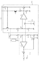
【0095】
次に、データバックアップ用のRAMを有するLSIのシャントレギュレータ回路に適用する本発明の第3の実施の形態を図3と共通の構成要素には共通の参照文字/数字を付して同様に回路図で示す図5を参照すると、この図に示す本実施の形態の前述の第2の実施の形態との相違点は、このシャントレギュレータ回路を持つLSIのデータバックアップ用のRAMの電源を、生成したリセット信号RBとバックアップ解除信号BRに基づき外部のバックアップ電源から電源VREG1に切り換えるためのバックアップ切換信号BUBを出力するバックアップ切換回路4を備えるとともに、その外部回路としてリセット信号RBとバックアップ解除信号BRを生成するためのそれぞれの一端を電源VREG1に接続した抵抗R1,R2と、それぞれの一端を抵抗R1,R2の各々の他端に接続しそれぞれの他端を接地に接続したコンデンサC1,C2と、NAND回路NA1の出力端に低電圧信号VLのバッファリング用のバッファB1とを備えることである。抵抗R1とコンデンサC1との共通接続点はリセット信号RBを、抵抗R2とコンデンサC2との共通接続点はバックアップ解除信号BRをそれぞれ生成する。
【0096】
バックアップ切換回路4は、入力端を抵抗R1の他端に接続したインバータI41と、ドレインを抵抗R2の他端にゲートをインバータI1の出力端にソースを接地にそれぞれ接続したNチャネルMOS型のトランジスタM41と、一方の入力端をNAND回路NA1の出力端に他方の入力端をトランジスタM41のドレインにそれぞれ接続し出力端からバックアップ切換信号BUBを出力するAND回路A41とを備える。
【0097】
一般に、この種のシャントレギュレータ回路を含むLSI(以下システム)のデータバックアップ用のRAMは、まず、バックアップ切換信号により、シャントレギュレータ回路の起動時は外部のバックアップ用電源を用いて動作し、シャントレギュレータ回路が立ち上がって2次電源が安定してからバックアップ切換信号を解除してバックアップ用電源からシャントレギュレータ回路の2次電源に切り換える。
【0098】
バックアップ切換信号の論理レベルを低電圧信号と同一にすると、システムのリセットの解除と同期してバックアップ切換信号も解除されるため、データバックアップ用RAMの電源が不安定となりデータが保持されなくなる。
【0099】
本実施の形態では、独立したリセット信号RBとバックアップ解除信号BRを設定し、外付け素子である抵抗R1,コンデンサC1及び抵抗R2,コンデンサC2の各々の時定数でもってこれらリセット信号RB及びバックアップ解除信号信号BRが動作する。
【0100】
ここで、バックアップ解除信号BRは、リセット信号RBの解除後に充電されるように設定している。
【0101】
AND回路A41はバックアップ解除信号BRと低電圧信号VLとを入力しそれらの論理積演算(AND)を行いバックアップ切換信号BUBを出力する。
【0102】
また、バッファB1は、バックアップ切換信号BUBと低電圧信号VLの同期をとるためのものである。
【0103】
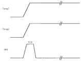
図5及び各信号波形をタイムチャートで示す図6を参照して本実施の形態の動作について説明すると、まず、起動時は、コンデンサC1に抵抗R1を経由して電圧Vreg1が充電されリセット信号RBの電圧が上昇し、リセット信号RBがI点の電圧に達するとリセットが解除される。
【0104】
リセットが解除されるとバックアップ解除信号BRは抵抗R2を経由してコンデンサC2によって充電される。
【0105】
2次電圧Vreg1/Vreg2が上昇し、H点の電圧に到達すると、低電圧信号VLは、Hレベルに遷移する。
【0106】
一方、バックアップ解除信号BRが上昇し、J点の電圧に達すると、低電圧信号VLとのANDによりバックアップ切換信号BUBがHレベルに遷移する。
【0107】
低電圧検出部12,22での低電圧検出時は、低電圧信号VLと同時にバックアップ切換信号BUBは遮断される。
【0108】
したがって、起動時は、レギュレータ部11,21の2次電源VREG1,VREG2が完全に立ち上がってからバックアップ用のRAMの電源をバックアップ電源から2次電源VREG1,VREG2に切換える。
【0109】
また、低電圧検出時は、2次電源VREG1,VREG2が立ち下がる前にバックアップ電源に切換える。
【0110】
これにより、データバックアップ用RAMの電源が安定に供給される。
【0111】
【発明の効果】
以上説明したように、本発明のシャントレギュレータ回路は、第1及び第2のレギュレータ部の各々の電圧制御用の帰還回路の一部を構成し2次電圧を予め定めた第1の電圧に分圧するための帰還用抵抗と低電圧信号検出部への入力電圧生成のため2次電圧を分圧するための分電圧抵抗とを兼用することにより、抵抗数及び抵抗に流れる電流を低減するとともに、低電圧検出電圧は2次電源電圧のサンプル電圧そのものであるので、抵抗値の相対的なずれが生じてもこれら電源電圧と低電圧検出電圧とが逆転することは起こり得ないという効果がある。
【0112】
また、第1及び第2のレギュレータ部の各々を同時に起動するための1つの起動用スイッチを備えることにより、複数のレギュレータ回路の起動は、一つの起動用のスイッチを用いて行うため同時に行われことにより、起動タイミングのずれ等の不具合が発生しないという効果がある。
【0113】
またさらに、コンパレータの基準電源の入力端にヒステリシス特性付加回路を備えることにより一定のヒステリシス特性(電圧)が得られ、出力電圧の低下時におけるヒステリシス特性の変動を防止して安定動作が実現できるという効果がある。
【図面の簡単な説明】
【図1】本発明のシャントレギュレータ回路の第1の実施の形態を示す回路図である。
【図2】本実施の形態のシャントレギュレータ回路における動作の一例を示すタイムチャートである。
【図3】本発明のシャントレギュレータ回路の第2の実施の形態を示す回路図である。
【図4】本実施の形態のシャントレギュレータ回路における動作の一例を示すタイムチャートである。
【図5】本発明のシャントレギュレータ回路の第3の実施の形態を示す回路図である。
【図6】本実施の形態のシャントレギュレータ回路における動作の一例を示すタイムチャートである。
【図7】従来の第1のシャントレギュレータ回路の一例を示す回路図である。
【図8】従来の第2のシャントレギュレータ回路の一例を示す回路図である。
【符号の説明】
1,2 レギュレータ回路
3 遮断信号検出回路
4 バックアップ切換回路
11,21,101,101A レギュレータ部
12,22,102 低電圧検出部
A41 AND回路
B1 バッファ
C1,C2 コンデンサ
CP11,CP21,CP31 コンパレータ
D1,D2 ダイオード
I41 インバータ
L1,L2 負荷
NA1 NAND回路
OP11,OP101 増幅器
M11,M12,M13,M21,M22,M23,M31,M32,M41,Q11,Q12,Q21,Q22 トランジスタ
R1,R2,R11,R12,R13,R14,R15,R16,R17,R18,R21,R22,R23,R24,R25,R26,R27,R28,R31,R32,R33 抵抗
VR1 基準電圧回路
Z1,Z2 ツェナーダイオード[0001]
TECHNICAL FIELD OF THE INVENTION
The present invention relates to a shunt regulator circuit, and more particularly to a shunt regulator circuit having a low-voltage detection function built in an LSI that requires two or more power supply voltages.
[0002]
[Prior art]
As this type of shunt regulator circuit, for example, one having two systems of secondary-side power supplies, monitoring both power supply voltages, and having a low-voltage signal output function and a backup switching signal output function is widely used.
[0003]
2. Description of the Related Art In recent years, along with miniaturization and high-speed operation of elements such as transistors constituting a large-scale semiconductor integrated circuit (LSI), the power supply voltage of a logic circuit inside the LSI has been rapidly decreasing. However, an input / output circuit (I / O) for interfacing with an analog circuit section or another external circuit is different from an internal logic circuit due to an operation limit of the analog circuit and a limitation of a power supply voltage of an LSI application. In many cases, a power supply voltage is used. In order to satisfy these requirements, it is necessary to supply two or more power supply voltages as a secondary power supply to be supplied to the inside of the LSI.
[0004]
Therefore, a shunt regulator circuit is used as a voltage conversion circuit to receive a supply of, for example, 5 V, which is currently widely used for a logic circuit as a primary power supply, and to output, for example, 3.3 V as a secondary power supply.
[0005]
The low voltage detection function monitors the secondary power supply generated as described above, and when the secondary power supply voltage drops for some reason, detects this drop and outputs a low voltage signal as an alarm.
[0006]
Referring to FIG. 7, which shows a circuit diagram of one system of a general conventional first shunt regulator circuit, the conventional first shunt regulator circuit receives a supply of a primary power supply VIN and a secondary power supply VREG. It includes a regulator section 101 for supplying the load L1, and a low
[0007]
The regulator unit 101 has one end connected to the primary power supply VIN, the other end connected to the power supply terminal TD1 that outputs the secondary power supply VREG having the voltage Vreg controlled, and one end connected to the resistor R106. , A resistor R11 having one end connected to the other end of the resistor R12 and the other end to the ground G, a reference voltage circuit VR1 for outputting a reference voltage VREF, and a non-inverting input terminal connected to a resistor R11. , R12, an operational amplifier (hereinafter referred to as an operational amplifier) having an inverting input terminal connected to the output terminal of the reference voltage circuit VR1 at a node A1 which is a common connection terminal of the amplifier OP101, a base connected to the output terminal of the amplifier OP101, and an emitter connected to ground G A collector is connected to one end of a load L1 having a collector connected to the other end of the resistor R106 and the other end to the ground. And a polar-type transistor Q101.
[0008]
The low-
[0009]
Next, the operation of the first conventional shunt regulator circuit will be described with reference to FIG. 7. When the primary-side power supply VIN is supplied, the regulator unit 101 supplies the following voltage to the secondary side. A power supply VREG of Vreg is generated.
[0010]
Vreg = VREF × (1 + R12 / R11) (1)
The shunt resistor R106 needs to be set to a resistance value equal to or smaller than the following equation, assuming that the load current is IL, and needs to be set to a considerably small value in consideration of the case where VIN decreases.
[0011]
R106 = (VIN−Vreg) / IL (2)
The current IS flowing through the shunt resistor R106 is represented by the following equation, where IY is a surplus current that is a current flowing to the ground via the control transistor Q11.
[0012]
IS = IL + IY = (VIN−Vreg) / R106 (3)
IY = IS-IL = (VIN-Vreg) / R106-IL (4)
From equation (4), it can be seen that the surplus current IY increases as the control range VIN-Vreg increases.
[0013]
The surplus current IY is absorbed by the control transistor Q101, but this current is wastefully consumed and causes an increase in current consumption. Therefore, the surplus current IY is not suitable for an application that is driven by a battery and that aims at low power consumption. .
[0014]
In the low
[0015]
The resistors R14 and R15 of the transistor M11 form a feedback circuit for adding hysteresis to add a predetermined hysteresis characteristic to the comparator CP11.
[0016]
One system of the second conventional shunt regulator circuit, which alleviates the above-mentioned problem and reduces power consumption, is provided with common reference characters / numerals for components common to FIG. Referring to FIG. 8, the difference between the conventional second shunt regulator circuit shown in FIG. 8 and the above-described conventional first shunt regulator circuit is that one end is connected to the primary power supply VIN instead of the regulator unit 101. A resistor R16 having the other end connected to the collector of the transistor Q11 and a collector connected to a common connection point between the other end of the resistor R16 and the collector of the transistor Q11 with the emitter connected to the primary power supply VIN instead of the shunt resistor R106. A PNP bipolar transistor Q12 connected to one end of L1 and a common connection point of resistors R12 and R13, and an amplifier OP101 An amplifier OP11 composed of an operational amplifier having an inverting input terminal connected to a node A1, which is a common connection terminal of the resistors R11 and R12, and a non-inverting input terminal connected to an output terminal of the reference voltage circuit VR1, and one end connected to the primary power supply VIN. A starting switch SW1 connected to one end of a resistor R17 described later, a resistor R17 having one end connected to the other end of the switch SW1 and the other end connected to the output end of the amplifier OP11, and one end connected to the other end of the resistor R17 and the amplifier OP11. And a resistor R18 having the other end connected to the ground at the common connection point with the output end of the regulator 101A.
[0017]
In the second conventional shunt regulator circuit, the regulator unit 101A performs voltage control using a voltage dropping transistor Q12 controlled by a feedback signal output from a control transistor Q11 instead of the shunt resistor R106. The surplus current is only a current of the transistor Q11 necessary for controlling the transistor Q12, that is, a current gain GI of the transistor Q12, and is small. However, since automatic startup cannot be performed only by turning on the power, a startup circuit including the switch SW1 and the resistors R17 and R18 must be provided.
[0018]
Therefore, when generating two or more types of secondary power supply voltages, two or more (a plurality of) similar circuits are provided.
[0019]
In this case, the low voltage signal VL is generally used as it is as a backup switching signal for switching to a redundant system.
[0020]
However, in the conventional second shunt regulator circuit, when a plurality of regulator circuits are incorporated in an LSI, it is necessary to accurately control the start timing of each of the plurality of regulator circuits, which makes the startup complicated. The malfunction of the application target system may cause malfunction or runaway due to a timing failure at the time of startup.
[0021]
The reason for this is that when an internal circuit is driven by two types of secondary voltages of a low voltage (for example, 2.5 V) and a high voltage (for example, 3.3 V) in an LSI incorporating a CPU, a low voltage If the high voltage side 3.3V rises later than the 2.5V side, the CPU may not be initialized properly and the system may run away.
[0022]
Further, since the gain of the feedback loop is high, even if the regulator circuit enters a cutoff state upon receiving a cutoff signal from the outside, the cutoff signal itself becomes unstable at the time of cutoff, and the cutoff may be released. At this time, if the regulator circuit can operate, there is a problem that the power supply is started again and the secondary power supply does not fall.
[0023]
Furthermore, when a plurality of regulator circuits and corresponding low-voltage detection circuits are incorporated in an LSI, a feedback resistor and a low-voltage detection resistor are provided independently of each other. Therefore, there is a problem that the circuit area increases with an increase in the number of resistors, and the current consumption increases due to an increase in the current flowing through the feedback resistor and the low-voltage detection resistor.
[0024]
Further, if the logic of the backup switching signal is the same as that of the low voltage signal, the backup switching signal is released in synchronization with the release of the reset of the system.
[0025]
[Problems to be solved by the invention]
In the first conventional shunt regulator circuit described above, the sum of the load current and the surplus current flowing through the control transistor flows through the shunt resistor, and the surplus current is absorbed by the control transistor. Is disadvantageously consumed because it is wastefully consumed and causes an increase in current consumption. Therefore, it is not suitable for low power consumption applications such as those driven by batteries.
[0026]
In the case where a plurality of regulator circuits corresponding to two or more types of secondary power supplies are incorporated in an LSI, the conventional second shunt regulator circuit which has alleviated the above-mentioned disadvantages accurately determines the start timing of each of the plurality of regulator circuits. In addition to this, there are disadvantages that the startup becomes complicated, and that a malfunction or a runaway of the application target system occurs due to a timing failure at the time of startup. In addition, since the gain of the feedback loop is high, even if the regulator circuit is in a cut-off state upon receiving a cut-off signal from the outside, when the cut-off is released due to the instability of the cut-off signal itself at the time of cut-off, the circuit is started again and the secondary power supply is started. However, there was a drawback that it did not fall. Furthermore, each of the plurality of regulator circuits and the corresponding low-voltage detection circuit independently includes a feedback resistor and a low-voltage detection resistor, so that the circuit area increases as the number of resistors increases. However, there is a disadvantage that the current consumption increases due to the increase in the current flowing through the device.
[0027]
An object of the present invention is to provide a shunt regulator with a low-voltage detection function in a regulator circuit built in an LSI requiring two or more types of power supply voltages, using one start-up SW1 to eliminate a start-up timing shift and to reduce the number of resistors. An object of the present invention is to provide a shunt regulator circuit that reduces the power consumption and the current consumption.
[0028]
Another object of the present invention is to provide a shunt regulator circuit in which when the secondary power supply is cut off, the secondary power supply does not start up again even if the cutoff signal becomes unstable.
[0029]
[Means for Solving the Problems]
The shunt regulator circuit according to the first aspect of the present invention is built in an LSI requiring two or more types of power supply voltages, and receives the supply of the primary power supply and outputs the stabilized first and second secondary power supplies, respectively. The first and second regulator units and the first and second secondary power supplies are monitored for the first and second voltages, respectively, and when the first and second voltages fall below a predetermined voltage. In a shunt regulator circuit including first and second low-voltage signal detectors for outputting first and second low-voltage signals for alarm, respectively, a reference voltage supplied to the first and second regulators A reference voltage circuit, a logic circuit that performs a logical operation on the first and second low-voltage signals and outputs an integrated low-voltage signal, and a start-up switch whose input terminal is connected to the primary power supply. , Each anode in front First and second diodes for preventing mutual interference connected to the output terminal of the switch, wherein each of the first and second regulator units has one end connected to the primary power supply and the other end described later. A first resistor connected to the collector of the first bipolar transistor, an emitter connected to the primary power supply, a base connected to a common connection point between the other end of the first resistor and the collector of the first bipolar transistor. Are connected to one end of a load whose other end is grounded, respectively, a second resistor whose one end is connected to the collector of the second bipolar transistor, and one end which is connected to the second bipolar transistor. A third resistor having the other end connected to ground at the other end of the resistor, and an inverting input terminal connected to a first node which is a common connection end of the second and third resistors, and a non-inverting input terminal connected to the reference. Voltage times And a second junction type first bipolar transistor having a base connected to the output terminal of the amplifier, an emitter connected to the ground, and a collector connected to the other end of the first resistor, respectively. A first resistor connected to the non-inverting input terminal of the amplifier and a fifth resistor connected to the other end of the fourth resistor; A sixth resistor having one end connected to the other end of the fifth resistor and the other end grounded, and a non-inverted input terminal connected to a common connection terminal of the fifth and sixth resistors and an inverting input terminal connected to the fifth resistor. A first comparator connected to a second node which is a common connection terminal of the second and third resistors, and a drain connected to the common connection terminal of the fourth and fifth resistors and a source connected to the fifth and sixth resistors. The gate is connected to the common connection terminal of the resistor, and the output terminal of the first comparator And a first MOS transistor of a first conductivity type respectively connected to the first MOS transistor.
[0030]
According to a second aspect of the present invention, in the shunt regulator circuit according to the first aspect, the first and second shunt regulator circuits further include a cutoff signal detection circuit that detects a cutoff signal supplied from outside and outputs a cutoff detection signal. Is provided with an output cutoff circuit for cutting off the output signal of the amplifier between the output terminal of the amplifier and the base of the first bipolar transistor in response to the supply of the cutoff detection signal. ing.
[0031]
According to a third aspect of the present invention, in the shunt regulator circuit according to the second aspect, the cutoff signal detection circuit connects a source to a secondary power supply, receives the cutoff signal at a gate, and receives the cutoff signal from a drain. A first MOS transistor of a first conductivity type having a source connected to the secondary power supply and a gate connected to the drain of the first MOS transistor, and an inverting input. An output terminal is connected to the drain of the second MOS transistor, a reference voltage is supplied to a non-inverting input terminal, and an output terminal is connected to the gate of the second transistor and the drain of the first transistor to output the cutoff detection signal. And a first resistor having one end connected to the secondary power supply and the other end connected to the drain of the second MOS transistor, respectively. A second resistor having one end connected to the other end of the first resistor and the other end connected to ground, and a third resistor having one end connected to the second power supply and the other end connected to the gate of the second MOS transistor, respectively. A third MOS transistor of a second conductivity type having a drain connected to the output terminal of the amplifier, a source connected to ground, and a gate supplied with the cutoff detection signal; A fourth MOS transistor of a second conductivity type having a gate connected to the second power supply, an output terminal of the amplifier, and a source connected to the base of the first bipolar transistor, and one end connected to the fourth MOS transistor. A constant current source connected to the source and the other end is grounded.
[0032]
According to a fourth aspect of the present invention, in the shunt regulator circuit according to the first aspect, a RAM for data backup of the LSI is provided, and an external backup is generated based on a reset signal and a backup release signal that generate power for the RAM. A backup switching circuit that outputs a backup switching signal for switching from a power supply to the secondary power supply, a first time constant circuit that includes a first time constant resistor and a first time constant capacitor and generates the reset signal, And a second time constant circuit that includes a second time constant resistor and a second time constant capacitor and generates the backup release signal.
[0033]
According to a fifth aspect of the present invention, in the shunt regulator circuit according to the fourth aspect, the backup switching circuit has an input terminal connected to the other end of the first time constant resistor having one end connected to the secondary power supply. A second conductivity type MOS transistor having a connected inverter, a drain connected to the other end of the second time constant resistor having one end connected to the secondary power supply, a gate connected to the output end of the inverter, and a source connected to ground. AND circuit for receiving a low-voltage signal for alarming a drop in the secondary power supply at one input terminal, connecting the other input terminal to the drain of the MOS transistor, and outputting the backup switching signal from an output terminal It is comprised including.
[0038]
BEST MODE FOR CARRYING OUT THE INVENTION
Next, embodiments of the present invention will be described in detail with reference to the drawings.
[0039]
A shunt regulator circuit according to the present embodiment is built in an LSI that requires two or more types of power supply voltages, and outputs first and second regulated power supplies, respectively, of first and second stabilized secondary power supplies; The first and second voltages of each of the first and second secondary power supplies are monitored, and when the first and second voltages fall below a predetermined voltage, the first and second voltages for alarming are monitored. In a shunt regulator circuit including first and second low-voltage signal detectors each outputting a low-voltage signal, the shunt regulator circuit constitutes a part of a feedback circuit for voltage control of the first regulator unit, and the first and second low-voltage signal detectors are connected to each other. A first feedback resistor for dividing the secondary voltage into a predetermined first voltage and a first secondary voltage for generating a first input voltage to the first low-voltage signal detector; And also serves as the first voltage-dividing resistor for A second feedback resistor for forming a part of a feedback circuit for voltage control of the second regulator unit for dividing the second secondary voltage into a predetermined second voltage; A second voltage dividing resistor for dividing the second secondary voltage in order to generate a second input voltage to the voltage signal detecting section; and each of the first and second regulator sections It is characterized in that it has one activation switch for simultaneous activation, and suppresses occurrence of a deviation in the activation timing of the first and second regulator units.
[0040]
Since the activation of the regulator circuit is performed using one activation SW, the activation of each power supply is performed almost simultaneously. Therefore, there is a feature that a timing deviation at the time of startup does not occur and a malfunction or a runaway of the application target system can be avoided.
[0041]
Further, by using the feedback resistor of the shunt regulator also as the low-voltage detection resistor, the number of resistors and the current flowing through the low-voltage detection resistor can be reduced.
[0042]
In addition, the low-voltage detector performs feedback for adding the hysteresis characteristic to the reference voltage side, so that the hysteresis characteristic does not change due to the change in the secondary power supply voltage.
[0043]
In addition, since the feedback resistor and the low-voltage detection resistor of the regulator circuit are also used, a dedicated low-voltage detection resistor is not required.
[0044]
Next, referring to FIG. 1 which is a circuit diagram of an embodiment of the present invention, in which constituent elements common to FIG. 8 are denoted by common reference characters / numerals, FIG. The shunt regulator circuit receives the supply of the primary power supply VIN, supplies the secondary power supplies VREG1 and VREG2 of the voltages Vreg1 and Vreg2 to the loads L1 and L2, and outputs the low voltage signals VL1 and VL2.
[0045]
The regulator circuit 1 monitors the
[0046]
The
[0047]
The
[0048]
The feedback circuit including the transistor M11 and the resistors R14 and R15 is for adding a hysteresis characteristic to the comparator CP11.
[0049]
The
[0050]
The
[0051]
The low-
[0052]
The feedback circuit including the transistor M21 and the resistors R24 and R25 is for adding a hysteresis characteristic to the comparator CP21.
[0053]
Next, the operation of the present embodiment will be described with reference to FIG. 1 and FIG. 2 showing each signal waveform in a time chart. Hereinafter, for convenience of explanation, the operation of the regulator circuit 1 will be described as a representative of the two identically configured
[0054]
First, in an initial state in which the power supply VIN is supplied, the control transistor Q11 of the
[0055]
Next, when the start switch SW1 is turned on, the voltage of the primary power supply VIN (hereinafter referred to as power supply VIN) is supplied to the node A3, whereby the base voltage of the transistor Q11 is determined by the ratio of the power supply VIN to the resistors R17 and R18. Is supplied, and the transistor Q11 which has been in the cut-off state is activated. As a result, a voltage drop corresponding to the collector current of the transistor Q11 occurs in the resistor R16, and a current flows due to a decrease in the base voltage of the transistor Q12, thereby generating the secondary power supply VREG1. At the node A1, a voltage determined by the ratio between the voltage Vreg1 of the power supply VREG1 and the resistors R12 and R11 is generated and applied to the inverting input terminal of the amplifier OP11. Here, for convenience of description, the resistor R12 is referred to as a feedback resistor of the
[0056]
Amplifier OP11 amplifies the difference voltage between the reference voltage supplied to the non-inverting input terminal and voltage VA1 at node A1, and supplies the output signal to the base of transistor Q11.
[0057]
The transistor Q11 increases or decreases the collector current in accordance with the supplied output signal of the amplifier OP11, and transmits the resulting change in the collector voltage to the base of the transistor Q12 as a change in the base current.
[0058]
That is, when the output signal of the amplifier OP11 increases and the collector current of the transistor Q11 increases, the collector voltage decreases due to the resistor R16, and the base emitter voltage of the PNP transistor Q12 increases, thereby increasing the base current of the transistor Q12. I do. Conversely, when the output signal of the amplifier OP11 decreases and the collector current of the transistor Q11 decreases, the base current of the transistor Q12 decreases.
[0059]
The transistor Q12 increases or decreases the output current in accordance with the increase or decrease in the base current, and adjusts the voltage Vreg1. As described above, the amplifier OP11, the transistor Q11, the resistor R16, the transistor Q12, and the resistors R12 and R11 form a feedback circuit for voltage control. Therefore, when the voltage VA1 at the inverting input terminal of the amplifier OP11 becomes the same as the reference voltage VR1 at the non-inverting input terminal, this voltage control operation is stabilized, and the power supply VREG1 having the constant voltage Vreg1 is output, and the load is output. L1.
[0060]
The
[0061]
As described above, since the voltage Vreg1 is output when the voltage VA1 of the node A1 is equal to the reference voltage VREF, the following equation is established.
[0062]
VA1 = R12 / (R11 + R12) = VREF (5)
VA1 / R11 = VREF / (R13 + R14 + R15) (6)
When the equation (5) is applied to the equation (6), the following equation is obtained.
[0063]
R11 = (R13 + R14 + R15) (7)
The voltage Vreg of the power supply VREG1 is expressed by the following equation.
[0064]
Vreg1 = VREF1 × {(R12 + R11) / R11} = VREF × {1 + R12 / (R13 + R14 + R15)} (8)
Similarly, the voltage Vreg2 of the power supply VREG2 is expressed by the following equation.
[0065]
Vreg2 = VREF × {1 + R22 / (R23 + R24 + R25)} · (9)
The activation of these
[0066]
The low
VM1 = VREF × (R15) / (R13 + R14 + R15) · (10)
The feedback circuit including the transistor M11 and the resistors R14 and R15 adds a predetermined hysteresis characteristic to the comparator CP11.
[0067]
In a normal state, the voltage VA1 which is a divided voltage between the feedback resistor R12 and the resistor R11 is higher than the voltage VM1, and the comparator CP11 outputs the L level as the low voltage signal VL1. Further, the transistor M11 is in a cutoff state.
[0068]
When the voltage VA1 decreases and becomes lower than the voltage VM1, the comparator CP11 makes a transition and outputs the H level as the low voltage signal VL1.
[0069]
At this time, the normally off transistor M11 conducts, and the resistor R14 is short-circuited. As a result, the voltage VM1 increases.
VM11 = VREF × (R15) / (R13 + R15) (11)
Therefore, even if the voltage VA1 rises, the comparator CP11 detects this new voltage VM.11, The H level is continuously output as the low voltage signal VL1. That is, by effectively increasing the voltage VM1 at the non-inverting terminal of the comparator CP11, the comparator CP11 has a hysteresis characteristic of maintaining the level of the low voltage signal VL1 so as not to be inverted even when the voltage VA1 increases.
[0070]
In this manner, the hysteresis characteristic (voltage) is made constant by providing the input terminal of the reference power supply of the comparator CP11 with the hysteresis characteristic, and the hysteresis characteristic fluctuation when the power supply voltage drops is prevented, thereby realizing a stable operation.
[0071]
Similarly, the low
[0072]
The NAND circuit NA1 performs a NAND operation on the low voltage signals VL1 and VL2 output from the
[0073]
When the voltages Vreg1 and Vreg2 of the power supplies VREG1 and VREG2 output from the
[0074]
As described above, in the shunt regulator circuit of the present embodiment, since the activation of the
[0075]
In addition, since the voltage dividing resistor for low voltage detection is also used as the feedback resistor R12 of the shunt regulator, the number of resistors is reduced, and the current flowing through the resistor is also reduced.
[0076]
Furthermore, since the voltage dividing resistor for low voltage detection is also used as the feedback resistor R12 of the shunt regulator, the voltages VA1 and VA2 of the detection point nodes A1 and A2, which are low voltage detection voltages, are equal to the secondary power supply voltage Vreg1. , Vreg2, the power supply voltages Vreg1 and Vreg2 and the low voltage detection voltage cannot be reversed even if the relative deviation of the resistance value occurs.
[0077]
Further, by providing the input end of the reference power supply of the comparator CP11 with a hysteresis characteristic, a constant hysteresis characteristic (voltage) is obtained, and a fluctuation in the hysteresis characteristic when the voltage Vreg is reduced is prevented to realize a stable operation. .
[0078]
Next, a second embodiment of the present invention will be described with reference to FIG. 3, which is also shown in a circuit diagram with common reference characters / numerals added to components common to FIG. This embodiment is different from the above-described first embodiment in that a cutoff
[0079]
The shutoff
[0080]
The output circuit breaker 13 includes an N-channel MOS transistor M12 having a drain connected to the output terminal of the amplifier OP11, a source connected to ground, and a gate receiving the shutoff detection signal SD, and a drain connected to the power supply VREG2 and a gate connected to the amplifier OP11. An output terminal includes an N-channel MOS transistor M13 having a source connected to the base of the transistor Q11, and a constant current source I11 having one end connected to the source of the transistor M13 and the other end grounded.
[0081]
The output circuit breaker 23 has an N-channel MOS transistor M22 having a drain connected to the output terminal of the amplifier OP21, a source connected to the ground, and a gate supplied with the shutoff detection signal SD, and a drain connected to the power supply VREG2 and a gate connected to the amplifier OP21. An output terminal includes an N-channel MOS transistor M23 having a source connected to the base of the transistor Q21, and a constant current source I21 having one end connected to the source of the transistor M23 and the other end grounded.
[0082]
The operation of the present embodiment will be described with reference to FIG. 3 and FIG. 4 showing each signal waveform in a time chart. Hereinafter, for convenience of explanation, the operation of the
[0083]
The comparator CP31 of the cutoff
[0084]
First, at the time of startup, it is necessary to cut off the feedback of the
[0085]
The threshold (threshold) voltage VTH of the comparator CP31 is expressed by the following equation.
[0086]
VTH = VREF × (1 + R31 / R32) = Vreg2 (12)
Therefore, at the time of startup, the outputs of the amplifiers OP11 and OP21 are cut off and the feedback circuit for voltage control does not operate until the threshold voltage VTH becomes Vreg2.
[0087]
Therefore, the secondary-side voltage rises momentarily, so that Zener diodes Z1 and Z2 for clamping are connected to each of the secondary-side power supplies VREG1 and VREG2 to suppress an excessive voltage rise.
[0088]
Next, with reference to FIG. 4 again, the shutoff operation of the present embodiment when the shutoff signal OFFB is input will be described. First, the
[0089]
When the voltages VReg2 and Vreg1 decrease and become equal to or lower than the low-voltage detection voltages of the low-
[0090]
At this point, the entire shunt regulator circuit is in the initial state, and when the cutoff signal OFFB is inverted to the H level, the cutoff state is released. However, as described above, since the rising edge detection comparator CP31 sets the threshold voltage VTH to the voltage Vreg2, this comparator CP31 rises during the rising period until the power supply VREG2 reaches the voltage Vreg2. The H level is output as the cutoff signal SD without detecting the state. Accordingly, the output circuit breakers 23 and 13 maintain the cutoff state without increasing the voltages Vreg2 and Vreg1 of the secondary power supplies VREG2 and VREG1 in order to continue the output cutoff of the amplifiers OP21 and OP11.
[0091]
The transistor M31 of the cutoff detection circuit conducts when the cutoff signal OFFB is inverted to the H level, and short-circuits the resistor R31. Therefore, at this time, the threshold voltage VTH of the comparator CP31 is set to the reference voltage VREF.
[0092]
Here, if the threshold voltage VTH of the comparator CP31 is set to be low, the shunt regulator circuit is in the initial state, and when the cutoff is released in this state, the comparator CP31 recognizes the rising state. , Output the L level as shown by the broken line. In the start state, the output signals of the amplifiers OP21 and OP11 are supplied to the transistors Q21 and Q11, so that the feedback circuit for voltage control operates, and the voltages Vreg2 and Vreg1 perform an unstable operation of starting again as indicated by the broken lines.
[0093]
In this embodiment, as described above, the threshold voltage VTH of the comparator CP31 is set to VTH = Vreg2 at the time of startup, and the feedback circuit is not operated until the secondary voltage Vreg2 exceeds VTH. By reducing the threshold voltage VTH to the reference voltage VREF, the shunt regulator circuit operates stably once the secondary voltage Vreg2 rises.
[0094]
When the low-level cutoff signal OFFB is input and the cutoff state is entered, the transistor M31 is cut off, and the threshold voltage VTH of the comparator CP31 rises to the voltage Vreg2, so that the restart is not performed even if the cutoff signal becomes unstable.
[0095]
Next, a third embodiment of the present invention applied to an LSI shunt regulator circuit having a RAM for data backup will be described in the same manner as in FIG. Referring to FIG. 5, which is different from the above-described second embodiment of the present embodiment, the power supply of the data backup RAM of the LSI having the shunt regulator circuit is generated. A
[0096]
The
[0097]
In general, a RAM for data backup of an LSI (hereinafter referred to as a system) including a shunt regulator circuit of this type operates using an external backup power supply when the shunt regulator circuit is activated by a backup switching signal. After the circuit has started up and the secondary power supply has stabilized, the backup switching signal is released and the backup power supply is switched to the secondary power supply of the shunt regulator circuit.
[0098]
If the logical level of the backup switching signal is the same as that of the low voltage signal, the backup switching signal is also released in synchronization with the release of the reset of the system, so that the power of the data backup RAM becomes unstable and the data cannot be held.
[0099]
In the present embodiment, an independent reset signal RB and backup release signal BR are set, and these reset signal RB and backup release are set by the time constants of the external elements, ie, the resistors R1, C1 and R2, and C2. The signal BR operates.
[0100]
Here, the backup release signal BR is set to be charged after the reset signal RB is released.
[0101]
The AND circuit A41 receives the backup release signal BR and the low voltage signal VL, performs a logical product operation (AND) thereof, and outputs a backup switching signal BUB.
[0102]
The buffer B1 is for synchronizing the backup switching signal BUB and the low voltage signal VL.
[0103]
The operation of the present embodiment will be described with reference to FIG. 5 and FIG. 6 showing each signal waveform in a time chart. First, at the time of startup, the capacitor C1 is charged with the voltage Vreg1 via the resistor R1, and the reset signal RB Is reset, and the reset is released when the reset signal RB reaches the voltage at the point I.
[0104]
When the reset is released, the backup release signal BR is charged by the capacitor C2 via the resistor R2.
[0105]
When the secondary voltages Vreg1 / Vreg2 increase and reach the voltage at the point H, the low voltage signal VL transitions to the H level.
[0106]
On the other hand, when the backup release signal BR rises and reaches the voltage at the point J, the backup switching signal BUB transitions to the H level due to AND with the low voltage signal VL.
[0107]
When the
[0108]
Therefore, at the time of startup, after the secondary power supplies VREG1 and VREG2 of the
[0109]
When detecting a low voltage, the power supply is switched to a backup power supply before the secondary power supplies VREG1 and VREG2 fall.
[0110]
Thus, the power of the data backup RAM is stably supplied.
[0111]
【The invention's effect】
As described above, the shunt regulator circuit of the present invention constitutes a part of the feedback circuit for controlling the voltage of each of the first and second regulator sections, and divides the secondary voltage into the predetermined first voltage. The number of resistors and the current flowing through the resistors are reduced by simultaneously using the feedback resistors for reducing the voltage and the voltage dividing resistors for dividing the secondary voltage for generating the input voltage to the low-voltage signal detection unit. Since the voltage detection voltage is the sample voltage of the secondary power supply voltage itself, there is an effect that the power supply voltage and the low voltage detection voltage cannot be reversed even if a relative shift occurs in the resistance value.
[0112]
In addition, by providing one activation switch for simultaneously activating each of the first and second regulator units, activation of a plurality of regulator circuits is performed simultaneously using one activation switch. As a result, there is an effect that a trouble such as a shift in the start timing does not occur.
[0113]
Further, by providing a hysteresis characteristic adding circuit at the input terminal of the reference power supply of the comparator, a constant hysteresis characteristic (voltage) can be obtained, and fluctuation of the hysteresis characteristic when the output voltage decreases can be prevented to realize a stable operation. effective.
[Brief description of the drawings]
FIG. 1 is a circuit diagram showing a first embodiment of a shunt regulator circuit of the present invention.
FIG. 2 is a time chart showing an example of an operation in the shunt regulator circuit of the present embodiment.
FIG. 3 is a circuit diagram illustrating a shunt regulator circuit according to a second embodiment of the present invention.
FIG. 4 is a time chart showing an example of an operation in the shunt regulator circuit of the present embodiment.
FIG. 5 is a circuit diagram showing a third embodiment of the shunt regulator circuit of the present invention.
FIG. 6 is a time chart illustrating an example of an operation in the shunt regulator circuit of the present embodiment.
FIG. 7 is a circuit diagram showing an example of a conventional first shunt regulator circuit.
FIG. 8 is a circuit diagram showing an example of a second conventional shunt regulator circuit.
[Explanation of symbols]
1,2 regulator circuit
3 Cutoff signal detection circuit
4 Backup switching circuit
11, 21, 101, 101A Regulator section
12,22,102 Low voltage detector
A41 AND circuit
B1 buffer
C1, C2 capacitors
CP11, CP21, CP31 Comparator
D1, D2 diode
I41 inverter
L1, L2 load
NA1 NAND circuit
OP11, OP101 Amplifier
M11, M12, M13, M21, M22, M23, M31, M32, M41, Q11, Q12, Q21, Q22 Transistors
R1, R2, R11, R12, R13, R14, R15, R16, R17, R18, R21, R22, R23, R24, R25, R26, R27, R28, R31, R32, R33
VR1 reference voltage circuit
Z1, Z2 Zener diode
Claims (5)
前記第1及び第2のレギュレータ部に供給する基準電圧を発生する基準電圧回路と、
前記第1及び第2の低電圧信号の論理演算を行い統合低電圧信号を出力する論理回路と、
入力端が前記1次電源に接続された起動用のスイッチと、
各々のアノードが前記スイッチの出力端に接続された相互干渉防止用の第1及び第2のダイオードとを備え、
前記第1及び第2のレギュレータ部の各々が、一端を前記1次電源に接続し他端を後述の第1のバイポーラトランジスタのコレクタに接続した第1の抵抗と、エミッタを前記1次電源にベースを前記第1の抵抗の他端と前記第1のバイポーラトランジスタのコレクタとの共通接続点にコレクタを他端が接地された負荷の一端にそれぞれ接続した第1接合型の第2のバイポーラトランジスタと、
一端を前記第2のバイポーラトランジスタのコレクタに接続した第2の抵抗と、
一端を前記第2の抵抗の他端に他端を接地にそれぞれ接続した第3の抵抗と、
反転入力端を前記第2,第3の抵抗の共通接続端である第1のノードに非反転入力端を前記基準電圧回路の出力端にそれぞれ接続した増幅器と、
ベースを前記増幅器の出力端にエミッタを接地にコレクタを前記第1の抵抗の他端にそれぞれ接続した第2接合型の前記第1のバイポーラトランジスタとを備え、
前記第1及び第2の低電圧検出部が、一端を前記増幅器の非反転入力端に接続した第4の抵抗と、
一端を前記第4の抵抗の他端に接続した第5の抵抗と、
一端を前記第5の抵抗の他端に他端を接地にそれぞれ接続した第6の抵抗と、
非反転入力端を前記第5及び第6の抵抗の共通接続端に反転入力端を前記第2,第3の抵抗の共通接続端である第2のノードにそれぞれ接続した第1のコンパレータと、
ドレインを前記第4,第5の抵抗の共通接続端にソースを前記第5,第6の抵抗の共通接続端にゲートを前記第1のコンパレータの出力端にそれぞれ接続した第1導電型の第1のMOSトランジスタとを備えることを特徴とするシャントレギュレータ回路。First and second regulator units which are built in an LSI requiring two or more types of power supply voltages and receive primary power supply and output stabilized first and second secondary power supplies, respectively; First and second voltages of each of the first and second secondary power supplies are monitored, and when the first and second voltages fall below a predetermined voltage, first and second low voltages for alarming; A shunt regulator circuit including first and second low-voltage signal detectors each outputting a signal.
A reference voltage circuit for generating a reference voltage to be supplied to the first and second regulator units;
A logic circuit that performs a logical operation of the first and second low-voltage signals and outputs an integrated low-voltage signal;
An activation switch having an input terminal connected to the primary power supply;
First and second diodes for preventing mutual interference, each anode being connected to the output terminal of the switch;
Each of the first and second regulator units has a first resistor having one end connected to the primary power supply and the other end connected to a collector of a first bipolar transistor described later, and an emitter connected to the primary power supply. A first junction-type second bipolar transistor having a base connected to a common connection point between the other end of the first resistor and the collector of the first bipolar transistor, and a collector connected to one end of a load having the other end grounded; When,
A second resistor having one end connected to the collector of the second bipolar transistor;
A third resistor having one end connected to the other end of the second resistor and the other end connected to ground,
An amplifier having an inverting input terminal connected to a first node that is a common connection terminal of the second and third resistors, and a non-inverting input terminal connected to an output terminal of the reference voltage circuit;
A second junction type first bipolar transistor having a base connected to an output terminal of the amplifier, an emitter connected to ground, and a collector connected to the other end of the first resistor, respectively.
A first resistor having one end connected to a non-inverting input terminal of the amplifier;
A fifth resistor having one end connected to the other end of the fourth resistor,
A sixth resistor having one end connected to the other end of the fifth resistor and the other end connected to ground,
A first comparator having a non-inverting input terminal connected to a common connection terminal of the fifth and sixth resistors and an inverting input terminal connected to a second node which is a common connection terminal of the second and third resistors;
A drain of a first conductivity type having a drain connected to a common connection terminal of the fourth and fifth resistors and a source connected to a common connection terminal of the fifth and sixth resistors and a gate connected to an output terminal of the first comparator, respectively. A shunt regulator circuit comprising one MOS transistor .
前記第1及び第2のレギュレータ部の各々が、前記増幅器の出力端と前記第1のバイポーラトランジスタのベースとの間に前記遮断検出信号の供給に応じて前記増幅器の出力信号を遮断する出力遮断回路を備えることを特徴とする請求項1記載のシャントレギュレータ回路。A cutoff signal detection circuit that detects a cutoff signal supplied from the outside and outputs a cutoff detection signal,
Each of the first and second regulator units interrupts an output signal of the amplifier between an output terminal of the amplifier and a base of the first bipolar transistor in response to supply of the interruption detection signal. The shunt regulator circuit according to claim 1, further comprising a circuit.
ソースを前記2次電源にゲートを前記第1のMOSトランジスタのドレインにそれぞれ接続した第1導電型の第2のMOSトランジスタと、
反転入力端を前記第2のMOSトランジスタのドレインに非反転入力端に基準電圧の供給を受け出力端を前記第2のトランジスタのゲート及び前記第1のトランジスタのドレインに接続して前記遮断検出信号を出力するコンパレータと、
一端を前記2次電源に他端を前記第2のMOSトランジスタのドレインにそれぞれ接続
した第1の抵抗と、
一端を前記第1の抵抗の他端に他端を接地にそれぞれ接続した第2の抵抗と、
一端を前記第2の電源に他端を前記第2のMOSトランジスタのゲートにそれぞれ接続
した第3の抵抗とを備え、
前記出力遮断回路が、ドレインを前記増幅器の出力端にソースを接地にそれぞれ接続しゲートに前記遮断検出信号の供給を受ける第2導電型の第3のMOSトランジスタと、
ドレインを前記第2の電源にゲートを前記増幅器の出力端にソースを前記第1のバイポーラトランジスタのベースにそれぞれ接続した第2導電型の第4のMOSトランジスタと、
一端を前記第4のMOSトランジスタのソースに接続し他端を接地した定電流源とを備えることを特徴とする請求項2記載のシャントレギュレータ回路。A first conductivity type first MOS transistor configured to connect the source to a secondary power supply, receive the cutoff signal at a gate, and output the cutoff detection signal from a drain;
A second MOS transistor of a first conductivity type having a source connected to the secondary power supply and a gate connected to the drain of the first MOS transistor, respectively;
An inverting input terminal is supplied to a drain of the second MOS transistor, a reference voltage is supplied to a non-inverting input terminal, and an output terminal is connected to a gate of the second transistor and a drain of the first transistor. And a comparator that outputs
A first resistor having one end connected to the secondary power supply and the other end connected to the drain of the second MOS transistor;
A second resistor having one end connected to the other end of the first resistor and the other end grounded;
A third resistor having one end connected to the second power supply and the other end connected to the gate of the second MOS transistor,
A third MOS transistor of a second conductivity type having a drain connected to an output terminal of the amplifier, a source connected to ground, and a gate supplied with the cutoff detection signal;
A fourth MOS transistor of a second conductivity type having a drain connected to the second power supply, a gate connected to the output terminal of the amplifier, and a source connected to the base of the first bipolar transistor;
3. The shunt regulator circuit according to claim 2, further comprising: a constant current source having one end connected to the source of the fourth MOS transistor and the other end grounded.
第1の時定数抵抗と第1の時定数コンデンサから成り前記リセット信号を生成する第1の時定数回路と、
第2の時定数抵抗と第2の時定数コンデンサから成り前記バックアップ解除信号を生成する第2の時定数回路とを備えることを特徴とする請求項1記載のシャントレギュレータ
回路。A backup switching circuit having a RAM for data backup of the LSI, and outputting a backup switching signal for switching from an external backup power source to the secondary power source based on a reset signal and a backup release signal for generating a power source for the RAM; ,
A first time constant circuit comprising a first time constant resistor and a first time constant capacitor for generating the reset signal;
Shunt regulator circuit according to claim 1, characterized in that it comprises a second time constant circuit for generating the backup release signal consists second constant resistor and a second time constant capacitor when.
ドレインを一端が前記2次電源に接続された前記第2の時定数抵抗の他端にゲートを前記インバータの出力端にソースを接地にそれぞれ接続した第2導電型のMOSトランジスタと、
一方の入力端に前記2次電源の低下を警報するための低電圧信号の供給を受け他方の入力端を前記MOSトランジスタのドレインに接続し出力端から前記バックアップ切換信号を出力するAND回路とを備えることを特徴とする請求項4記載のシャントレギュレータ回路。An inverter having an input terminal connected to the other end of the first time constant resistor having one end connected to the secondary power supply;
A second conductivity type MOS transistor having a drain connected to the other end of the second time constant resistor having one end connected to the secondary power supply, a gate connected to the output end of the inverter, and a source connected to ground;
An AND circuit that receives a low-voltage signal for alarming a drop in the secondary power supply at one input terminal, connects the other input terminal to the drain of the MOS transistor, and outputs the backup switching signal from an output terminal. The shunt regulator circuit according to claim 4, further comprising:
Priority Applications (1)
| Application Number | Priority Date | Filing Date | Title |
|---|---|---|---|
| JP2000288519A JP3602425B2 (en) | 2000-09-22 | 2000-09-22 | Shunt regulator circuit |
Applications Claiming Priority (1)
| Application Number | Priority Date | Filing Date | Title |
|---|---|---|---|
| JP2000288519A JP3602425B2 (en) | 2000-09-22 | 2000-09-22 | Shunt regulator circuit |
Publications (2)
| Publication Number | Publication Date |
|---|---|
| JP2002099335A JP2002099335A (en) | 2002-04-05 |
| JP3602425B2 true JP3602425B2 (en) | 2004-12-15 |
Family
ID=18772096
Family Applications (1)
| Application Number | Title | Priority Date | Filing Date |
|---|---|---|---|
| JP2000288519A Expired - Fee Related JP3602425B2 (en) | 2000-09-22 | 2000-09-22 | Shunt regulator circuit |
Country Status (1)
| Country | Link |
|---|---|
| JP (1) | JP3602425B2 (en) |
Families Citing this family (1)
| Publication number | Priority date | Publication date | Assignee | Title |
|---|---|---|---|---|
| CN109474180A (en) * | 2018-11-05 | 2019-03-15 | 四川神坤电液控制技术有限公司 | Non-isolated buck-boost power supply circuits and power modules |
-
2000
- 2000-09-22 JP JP2000288519A patent/JP3602425B2/en not_active Expired - Fee Related
Also Published As
| Publication number | Publication date |
|---|---|
| JP2002099335A (en) | 2002-04-05 |
Similar Documents
| Publication | Publication Date | Title |
|---|---|---|
| US7746044B2 (en) | Power supply system for motherboard | |
| US7683592B2 (en) | Low dropout voltage regulator with switching output current boost circuit | |
| CN113110694B (en) | Low dropout regulator circuit with current surge suppression | |
| US7259543B2 (en) | Sub-1V bandgap reference circuit | |
| US20150188421A1 (en) | Voltage regulator | |
| US20030218454A1 (en) | Voltage mode voltage regulator with current mode start-up | |
| US10216210B2 (en) | Dual input power management method and system | |
| US20070194768A1 (en) | Voltage regulator with over-current protection | |
| JP2004005670A (en) | Low dropout regulator comprising current feedback amplifier and compound feedback loop | |
| CN101568893A (en) | Soft-start circuit and method for power-up of an amplifier circuit | |
| JP2010224825A (en) | Semiconductor integrated circuit | |
| WO2009078345A1 (en) | Constant voltage circuit | |
| JP2009199501A (en) | Voltage regulator | |
| EP1063578B1 (en) | Reference voltage generator with monitoring and start up means | |
| JP2006133936A (en) | Power supply device and portable device | |
| CN218122537U (en) | LDO circuit, power management system and main control chip | |
| US6310467B1 (en) | LDO regulator with thermal shutdown system and method | |
| JP2005157591A (en) | Thermal shutdown circuit | |
| JP2004070827A (en) | Constant voltage power supply circuit | |
| US7405545B2 (en) | Voltage-regulator and power supply having current sharing circuit | |
| TW201821927A (en) | Voltage regulators | |
| JP3602425B2 (en) | Shunt regulator circuit | |
| US20250004493A1 (en) | Voltage Regulation | |
| JP2008171177A (en) | Power circuit | |
| CN114257070B (en) | Hot plug protection device |
Legal Events
| Date | Code | Title | Description |
|---|---|---|---|
| A521 | Written amendment |
Free format text: JAPANESE INTERMEDIATE CODE: A523 Effective date: 20040116 |
|
| RD01 | Notification of change of attorney |
Free format text: JAPANESE INTERMEDIATE CODE: A7421 Effective date: 20040116 |
|
| A02 | Decision of refusal |
Free format text: JAPANESE INTERMEDIATE CODE: A02 Effective date: 20040608 |
|
| A521 | Written amendment |
Free format text: JAPANESE INTERMEDIATE CODE: A523 Effective date: 20040701 |
|
| A911 | Transfer of reconsideration by examiner before appeal (zenchi) |
Free format text: JAPANESE INTERMEDIATE CODE: A911 Effective date: 20040713 |
|
| TRDD | Decision of grant or rejection written | ||
| A01 | Written decision to grant a patent or to grant a registration (utility model) |
Free format text: JAPANESE INTERMEDIATE CODE: A01 Effective date: 20040831 |
|
| A61 | First payment of annual fees (during grant procedure) |
Free format text: JAPANESE INTERMEDIATE CODE: A61 Effective date: 20040922 |
|
| R150 | Certificate of patent or registration of utility model |
Free format text: JAPANESE INTERMEDIATE CODE: R150 |
|
| LAPS | Cancellation because of no payment of annual fees |