JP3598756B2 - Image display method, image display apparatus for performing the method, and image processing apparatus using the apparatus - Google Patents
Image display method, image display apparatus for performing the method, and image processing apparatus using the apparatus Download PDFInfo
- Publication number
- JP3598756B2 JP3598756B2 JP24188797A JP24188797A JP3598756B2 JP 3598756 B2 JP3598756 B2 JP 3598756B2 JP 24188797 A JP24188797 A JP 24188797A JP 24188797 A JP24188797 A JP 24188797A JP 3598756 B2 JP3598756 B2 JP 3598756B2
- Authority
- JP
- Japan
- Prior art keywords
- image data
- image
- output
- line
- transfer
- Prior art date
- Legal status (The legal status is an assumption and is not a legal conclusion. Google has not performed a legal analysis and makes no representation as to the accuracy of the status listed.)
- Expired - Fee Related
Links
Images


Landscapes
- Image Input (AREA)
- Closed-Circuit Television Systems (AREA)
- Television Systems (AREA)
- Controls And Circuits For Display Device (AREA)
Description
【0001】
【産業上の利用分野】
この発明は、2次元個体撮像素子を具備する撮像手段から出力された画像データをモニタに表示するための方法および装置、ならびにその表示装置を備えた画像処理装置に関連する。
【0002】
【従来の技術】
CCD撮像素子に代表される2次元の個体撮像素子では、フォトダイオードやフォトトランジスタなどのフォトセンサを複数個マトリクス状に配列して、各フォトセンサ毎に入射された光情報に比例する信号電荷を蓄積することにより、2次元画像データを生成している。各フォトセンサに蓄積された信号電荷は、インターライン転送方式やフレーム転送方式などの転送方法により1次元の映像信号として外部に出力される。
【0003】
図17は、インターライン転送方式型のCCD撮像素子の基本構成を示すもので、m列×n行のマトリクス状に配列された複数個のフォトセンサPhと、これらフォトセンサPhの列毎に配備されるm個の垂直シフトレジスタVR1〜VRmと、各垂直シフトレジスタVR1〜VRmの出力側に配備される水平シフトレジスタHRとを、主要構成として備えている。
【0004】
なおこの図示例では、説明を簡易化するために、1フィールド分の画像を生成するための構成のみを示してあり、各垂直シフトレジスタVR1〜VRmの各転送部には、それぞれその転送部に電荷を移送するフォトセンサPhがn行×m列のマトリクスのどの位置にあるかを示すアドレスが示してある。また水平シフトレジスタHRの各転送部に示される数値は、それぞれその転送部に何列目のフォトダイオードPhからの電荷が転送されるかを示すものである。また図中7は、出力バッファを示す。
【0005】
各垂直シフトレジスタVR1〜VRm,水平シフトレジスタHRは、CCD(電荷結合素子)により構成されており、各フォトセンサPh,垂直シフトレジスタVR1〜VRm,水平シフトレジスタHRは、それぞれ図示しない駆動部よりビデオ規格に基づくタイミングで与えられる転送パルスTP1,TP2,TP3を受けて、内部に蓄積された信号電荷を移送する。
【0006】
図18は、上記構成における信号電荷の出力動作のタイミングを示す。なお図中、1垂直期間毎の出力タイミング(上段)の1ライン分の出力データには、それぞれそのデータが何ライン目のフォトセンサPhに対応するかを示す数値が、また各水平期間毎の詳細な出力タイミング(下段)の1画素分の出力データには、そのデータに対応するフォトセンサPhのアドレスが、それぞれ示されている。
【0007】
まず最初の垂直期間が開始され、垂直ブランキング期間内に第1の転送パルスTP1が出力される。この転送パルスTP1は各フォトセンサPhに同時に与えられ、それぞれのフォトセンサPhに蓄積された電荷が対応する垂直シフトレジスタVR1〜VRmに一斉に移送される。
【0008】
つぎに第1の水平期間が開始され、水平ブランキング期間内に、各垂直シフトレジスタVR1〜VRmに第2の転送パルスTP2が与えられる。この転送パルスTP2により、各垂直シフトレジスタVR1〜VRm内の信号電荷は1画素ずつシフトされて、一番先頭の1ライン分の信号電荷(図中、アドレス(1,1)(2,1)・・・(m,1)の画素に対応する電荷)が水平シフトレジスタHR側へと移送される。
【0009】
ついで1水平期間が終了するまでの間に、水平シフトレジスタHRに対し、第3の転送パルスTP3がm個連続して与えられる。これにより水平シフトレジスタHR内に蓄積された1ライン分の信号電荷は1画素ずつシフトされ、最前方の電荷より順次出力される。
【0010】
以下同様にして、各水平期間毎に各垂直シフトレジスタVR1〜VRmに転送パルスTP2が与えられて、1ライン分の信号電荷が水平シフトレジスタHRへと移送された後、水平シフトレジスタHR側にm個の転送パルスTP3が与えられて前記転送された1ライン分の信号電荷が1画素ずつ出力される。この水平期間がn回繰り返されることにより1垂直期間が終了する。
【0011】
図19は、上記の動作により生成された2次元画像のデータ構成を示すもので、各フォトセンサPhに対応する各画素がフォトセンサの配列状態と同様のマトリクス状に配置された画像データが生成される。
【0012】
【発明が解決しようとする課題】
上記インターライン方式の個体撮像素子を用いた撮像装置は、現行のビデオ規格に伴い、1フィールド分の映像信号を1/60秒の時間間隔で出力するように設定されている。したがってこの現行の方式により出力される映像信号を画像処理装置に取り込んで処理を行う場合、入力された映像信号をリアルタイムで処理しても1秒間に60回の処理を行うのが限度であり、それ以上の高速化は図れないという問題がある。
【0013】
そこで出願人は、上記構成の個体撮像素子を用いて、1水平期間内に複数ライン分の画像データを1ライン分の画像データに変換して出力し、1垂直期間を短縮させるように改良された撮像装置を開発した。この撮像装置は、詳細は後記するが、1水平ブランキング期間内に各垂直シフトレジスタVR1〜VRmに与える転送パルスTP2を複数個設定することにより、各シフトレジスタVR1〜VRmからそれぞれ複数画素分の信号電荷を出力し、これら電荷を水平シフトレジスタHRより1水平期間内に出力するようにしたものである。この撮像装置を用いることにより1垂直期間を大幅に短縮して画像生成時間を高速化できるので、従来の制限値にとらわれずに画像処理時間を短縮することができる。
【0014】
ところで画像処理による各種の計測処理では、一般に、撮像手段から出力された画像データをモニタに表示させ、オペレータが表示画面上で対象物を確認したり、計測領域を設定するなどの処理を実施するケースが多い。しかしながらモニタは、通常のビデオ規格のタイミングで映像信号を受け取るように構成されているため、ビデオ規格外の方法で生成された画像データを表示することは不可能である。
【0015】
この発明は、上記問題点に着目してなされたもので、ビデオ規格外の方法で生成された画像データをモニタ表示可能とし、ビデオ規格外の画像データを処理する際にも通常と同様に目視確認や設定処理を行えるようにすることを技術課題とする。
【0016】
【課題を解決するための手段】
請求項1の発明は、2次元撮像素子と、この2次元撮像素子を、1垂直期間中の各水平期間毎に、それぞれあらかじめ設定された数のライン分の画像データを1ライン分の画像データに変換して出力するように駆動する駆動手段とを具備する撮像手段が出力した画像データを取り込んで、モニタに表示するための方法であって、前記2次元撮像素子に結像する原画像中の所定の領域に対応する画像データが1ラインずつ転送される一方、前記領域外の画像データが複数ラインずつ転送されるように、各水平期間毎の転送ライン数を設定しておき、前記撮像手段より各水平期間毎に出力された画像データをそのデータ出力速度に応じたタイミングで順次メモリに記憶するとともに、前記メモリ内の各画像データを、それぞれそのデータに対応する転送ライン数と同じ回数だけ読み出してモニタに出力する処理を、前記モニタの画像表示速度に応じたタイミングで順に実行することを特徴とする。
【0018】
請求項2の発明は、前記撮像手段から出力された画像データを取り込んでモニタに表示する画像表示装置にかかるものである。この装置は、前記2次元撮像素子に結像する原画像中の所定の領域に対応する画像データが1ラインずつ転送される一方、前記領域外の画像データが複数ラインずつ転送されるように、各水平期間毎の転送ライン数を設定する設定手段と、前記設定手段により設定された各水平期間毎の転送ライン数を前記撮像手段に転送する転送手段と、前記撮像手段から出力された各水平期間毎の画像データを順次記憶するための第1のメモリと、前記設定手段により設定された各水平期間毎の転送ライン数を記憶する第2のメモリと、前記各水平期間毎の画像データを撮像手段の出力速度に応じたタイミングで前記第1のメモリに記憶させる画像データ書込み手段と、前記第1のメモリに記憶された各画像データを、それぞれ第2のメモリ内の対応する転送ライン数と同じ回数だけ読み出してモニタに出力する処理を、前記モニタの画像表示速度に応じたタイミングで順に実行する画像データ出力手段とを具備している。
【0020】
請求項3の発明は、2次元撮像素子と、この2次元撮像素子を、1垂直期間中の各水平期間毎に、それぞれあらかじめ設定された数のライン分の画像データを1ライン分の画像データに変換して出力するように駆動する駆動手段とを具備する撮像手段と、前記撮像手段より出力された画像データを取り込んで所定の計測処理を実施する画像処理手段と、前記撮像手段からの画像データを表示するためのモニタとから成る画像処理装置にかかるもので、前記画像処理手段に、請求項2の画像表示装置と同様の構成を具備させている。
【0022】
【作用】
各請求項にかかる発明とも、撮像手段から各水平期間毎に出力された画像データを、撮像手段のデータ出力速度に応じたタイミングで順次メモリに記憶する一方、各記憶データを、それぞれそのデータに対応する転送ライン数と同じ回数だけ読み出してモニタに出力する処理を、モニタの画像表示速度、すなわちビデオ規格に応じたタイミングで順に実行する。
【0024】
このような制御により、モニタには、ビデオ規格に応じたタイミングで、かつビデオ規格に応じたライン数分の画像データが出力されるので、撮像手段により生成された画像をモニタ上に表示することが可能になる。
【0025】
また、撮像手段側は、2次元撮像素子に結像する原画像中の所定の領域に対応する画像データを1ラインずつ転送する一方、前記領域外の画像データが複数ラインずつ転送するように設定される。よって、計測対象物を含むように前記領域を設定すれば、計測対象物について、本来と同様の解像度による画像データを取得することができる。
【0026】
【実施例】
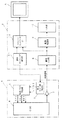
図1は、この発明の1実施例にかかる画像処理装置の構成を示すもので、2次元画像の映像信号を生成して出力する撮像装置1と、この撮像装置1から出力される映像信号を取り込んで所定の計測処理を実施する制御処理装置2と、撮像装置1により得られた画像を表示するためのモニタ3とを、主要構成として備えている。
【0027】
前記撮像装置1は、個体撮像素子としてCCD撮像素子3(図中「CCD」と略す)を具備するほか、転送パルス発生部5,転送ライン数指定部6,出力バッファ7などを構成として備えている。
【0028】
制御処理装置2は、撮像装置1からの映像信号をA/D変換するための画像入力部8,変換処理後のディジタル画像を用いて所定の計測処理を実施する画像処理部9,この画像処理結果を外部に出力するための出力部10のほか、モニタ3に表示用の画像データを出力するための構成として、表示タイミング発生部11,スキャンコンバータ部12(詳細は後記する)を具備している。
【0029】
CCD撮像素子3は、前記した図17と同一の構成を備えるもので、転送パルス発生部5より出力される第1〜第3の転送パルスTP1〜TP3を受けて動作する。すなわち第1の転送パルスTP1が与えられる毎に、各フォトセンサPhに蓄積された信号電荷が垂直シフトレジスタVR1〜VRmに転送され、第2の転送パルスTP2が与えられる毎に、各垂直シフトレジスタVR1〜VRmの蓄積電荷が1画素ずつ走査されて、先頭の1ライン分の信号電荷が水平シフトレジスタHRに転送される。さらに第3の転送パルスTP3が与えられる都度、水平シフトレジスタHRに蓄積された信号電荷が1画素ずつシフトされ、先頭の信号電荷が出力バッファ7を介して制御処理装置2側へと出力される。
【0030】
この実施例の撮像装置1は、1水平ブランキング期間内に前記第2の転送パルスTP2を複数個出力することにより、1水平期間毎に複数ライン分の映像信号を重畳して出力するように構成されている。前記転送ライン数指定部6は、1水平期間内に何ライン分の画像データを転送するかを設定するためのもので、設定された転送ライン数は、2ビット構成の転送ライン数信号L1,L2に変換されて前記転送パルス発生部5に出力される。
【0031】
図2は、前記転送ライン数毎の転送ライン数信号L1,L2のデータ構成を示すもので、1〜4までの各転送ライン数について、それぞれ「00」「10」「01」「11」のコードが割り当てられて、そのコードの上位ビットがL1として、下位ビットがL2として、それぞれ設定されている。
【0032】
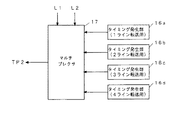
前記転送パルス発生部5における第2の転送パルスTP2の生成部は、図3に示すように、4個のタイミング発生部16a〜16dと各タイミング発生部16a〜16dを接続するマルチプレクサ17とにより構成される。
【0033】
前記各タイミング発生部16a〜16dは、それぞれ1〜4ライン分の転送用に用いられるもので、通常のビデオ規格の水平ブランキング期間と同じ長さの期間内に、対応する転送ライン数分のパルス信号を出力する(すなわち1水平ブランキング期間内に第1のタイミング発生部16aは1個、第2のタイミング発生部16bは2個、第3のタイミング発生部16cは3個、第4のタイミング発生部16dは4個のパルス信号を、それぞれ出力する)。
【0034】
マルチプレクサ17は、これらタイミング発生部16a〜16dの中から前記転送ライン数信号L1,L2の示す転送ライン数用のタイミング発生部を選択し、その信号の入力経路をCCD撮像素子4への出力経路に接続する。これにより選択されたタイミング発生部の出力パルスが前記転送パルスTP2として採用され、CCD撮像素子4へと与えられる。
【0035】
なおここでは図示しないが、第1の転送パルスTP1の生成部も、上記と同様に、各転送ライン数用の4個のタイミング発生部とマルチプレクサとにより構成される。このうち1ライン転送用のタイミング発生部は、通常のビデオ規格に基づくタイミングでパルス信号を1個出力するのに対し、2ライン〜4ライン転送用の各タイミング発生部は、通常の垂直期間に対しそれぞれ1/2,1/3,1/4の時間間隔毎にパルス信号を1個出力する。マルチプレクサが前記と同様に転送ライン数信号L1,L2に対応するタイミング発生部を選択することにより、そのタイミング発生部の出力パルスが転送パルスTP1として出力され、CCD撮像素子4に与えられる。
【0036】
つぎに図4により、上記撮像装置1における映像信号の出力動作の具体例をあげて説明する。なお以下の各実施例では、説明を簡単にするために、通常のビデオ規格における1フィールド分の画像のライン数(すなわち前記フォトセンサPhの行数n)を「200」と仮定している。
【0037】
図4は、各水平期間毎に2ライン分の映像信号を転送するように設定した場合の映像信号の出力タイミングを示すもので、図中、1垂直期間毎の出力タイミング(上段)の1ライン分の出力データには、そのデータが何ライン目のフォトセンサPhに対応するデータであるかを示す数値が示されている。また各水平期間毎の詳細な出力タイミング(下段)の1画素分の出力データには、そのデータに対応するフォトセンサPhのアドレスが示してある。
【0038】
転送パルス発生部5の転送信号TP1,TP2の各生成部では、それぞれ転送ライン数信号L1,L2に対応する2ライン転送用のタイミング制御部が選択されている。まず選択されたタイミングで第1の転送パルスTP1が出力されると、前記CCD撮像素子4の各フォトセンサPhの蓄積電荷が対応する垂直シフトレジスタVR1〜VRmへと移送され、垂直期間が開始される。
【0039】
つぎに転送パルス発生部5は、最初の水平ブランキング期間内に、各垂直シフトレジスタVR1〜VRmに対し、それぞれ2個の転送パルスTP2を出力する。これにより各垂直シフトレジスタVR1〜VRmの蓄積電荷は2画素分ずつシフトされ、第1ライン目と第2ライン目の信号電荷が連続して水平シフトレジスタHR側へと移送される。
【0040】
上記の動作により、水平シフトレジスタHRの各転送部には、同列の2画素分の信号電荷が重畳されて蓄積される。
つぎに転送パルス発生部5が、第3の転送パルスTP3を1水平ラインの画素数(m個)分生成して出力すると、水平シフトレジスタHRに蓄積された各重畳電荷が順次出力される。これにより最初の水平期間では1ライン目と2ライン目との2ライン分の映像信号が重畳された信号が出力されることになる。
【0041】
以下各水平期間毎に同様の動作を繰り返すことにより、それぞれ2ライン分の映像信号が重畳されて1ライン分の映像信号として出力される。この結果、つぎの転送信号TP1が出力されるまでの100回の水平期間により、各フォトセンサPhにより生成されたすべての信号電荷が出力される。
【0042】
図5は、上記動作により制御処理装置2に出力される2次元画像のデータ構成を示す。各ライン毎の画像データは、本来の画像の2ライン分の画像データが加算されたデータに相当し、縦方向のライン数は本来の1/2に減縮される。
【0043】
このように各水平期間毎に2ライン分の映像信号を1ライン分の映像信号として出力することにより、画像の解像度は劣化するが、画像の生成速度は従来の1/2の長さに短縮される。
【0044】
図1に戻って、制御処理装置2の画像入力部8は、撮像装置1より上記の動作タイミングに応じて出力された映像信号をリアルタイムで取り込んでA/D変換し、ディジタル量の画像データを生成する。このディジタル量の入力画像データは、前記画像処理部9に与えられると同時に、スキャンコンバータ部12へと出力される。
【0045】
画像処理部9は、図5に示した画像データに対し、例えば、2値化処理,エッジ抽出処理などの手法を用いて画像上の対象物を抽出した後、抽出された対象物について、面積,重心位置などの特徴量を計測するもので、さらに必要に応じてこの計測結果をあらかじめ設定された基準値と比較して対象物の良否を判定する。この計測結果や判定結果は、出力部9を介してモニタ3やその他の外部装置に出力される。
【0046】
上記の処理は、前記したように、従来の1/2の時間間隔で入力される画像データに対して行われるので、この画像入力のタイミングに合わせて計測処理を実施することにより、計測処理を高速化できる。この場合、入力画像の解像度は通常の画像の1/2に縮小されているので、処理の負担は大幅に軽減される。
【0047】
表示タイミング発生部11は、ビデオ規格に応じた垂直同期信号VD,水平同期信号HDを生成してスキャンコンバータ部12に出力する。スキャンコンバータ部12は、これら同期信号に応じて上記の計測処理とは独立に動作し、前記入力画像データから表示用の画像データを生成してモニタ3へと出力する。
【0048】
図6は、前記スキャンコンバータ部12の詳細な構成を示すもので、リード/ライト制御部13,フィールドメモリ14,D/A変換部15などにより構成される。
【0049】
フィールドメモリ14は、前記画像入力部8からの画像データを格納するためので、1フィールド分(すなわち100ライン分)の画像データを格納するためのエリアを具備する。リード/ライト制御部13は、このフィールドメモリ14に対するデータ書込み処理とデータ読出し処理とを、独立して制御するためのもので、データ書込み処理は前記画像データの入力タイミング(すなわち撮像装置1の画像出力タイミング)に応じて、データ読出し処理は前記タイミング制御部11の各同期信号に応じて、それぞれ実施される。フィールドメモリ14より読み出された画像データは、D/A変換部15によりアナログ量の映像信号に変換されてモニタ3に出力される。
【0050】
図7は、撮像装置1の1垂直期間にCCD撮像素子4の各フォトセンサPhに入射した光像(以下これを「原画像」という)、この原画像の画像データが図4の動作タイミングにより出力された場合にフィールドメモリ14に記憶される入力画像、フィールドメモリ14から読み出されて生成される表示画像の各画像について、それぞれ各ライン毎の画像データの対応関係を示したものである。なお図中、原画像のデータ種別はA、入力画像のデータ種別はB、表示用画像のデータ種別はCとおかれ、それぞれの画像の1ライン分の画像データは、そのデータ種別とライン位置を示す数値とにより表されている。また20a,20b,20cは、各画像上の計測対象物の画像を示す。
【0051】
前記図4の動作タイミングおよび図5のデータ構成図に示したように、撮像装置1からは、各水平期間毎にそれぞれ原画像の2ライン分の映像信号が重畳された映像信号が出力される。フィールドメモリ14には、この映像信号をディジタル変換した画像データがリアルタイムで読み込まれるので、各エリアには、それぞれ原画像の2ライン分の画像データが加算された画像データB1〜B100が順次書き込まれる。
【0052】
リード/ライト制御部13は、この書込み動作とは独立して、フィールドメモリ14の各エリアに格納された画像データB1〜B100を、それぞれ各画像データに対応する転送ライン数分、すなわち2回ずつ読み出して、通常のビデオ規格に応じた200ライン分の画像データC1〜C200を生成する。このデータ読出し動作は、前記表示タイミング発生部11より与えられる水平同期信号VDに応じて行われるもので、読み出された各画像データC1〜C200のアナログ変換後の信号は、インターレス方式に基づき、順次モニタ3の画面上に走査される。
【0053】
なおこの図7では、各画像間のデータの対応関係を明確にするために、フィールドメモリ14内の1フィールド分の画像データB1〜B100から1フィールド分の表示画像データC1〜C200が生成されるように示してある。しかしながら実際の動作においては、書込み動作は読出し動作の2倍の速度で行われているので、撮像装置1側で1垂直期間が終了すると、先の垂直期間分の画像データの読出しが完了したか否かにかかわらず、フィールドメモリ14の各エリアのデータが順に書き換えられる。したがって、フィールドメモリ14より読み出される1フィールド分の表示画像データには、撮像装置1側の2フィールド分の画像データが混在することになる。
【0054】
図8は、前記フィールドメモリ14に対する書込みおよび読出し動作のタイミングを示す。図中、Bは撮像装置1からの奇数フィールド分の入力画像データを、B´は偶数フィールド分の入力画像データを、それぞれ示す。
【0055】
前記リード/ライト制御部13は、フィールドメモリ14に対し、撮像装置1側の垂直期間、すなわちビデオ規格の半分の期間毎に、データの書換えを実施するとともに、ビデオ規格に基づく垂直期間毎に各フィールドメモリ14の各データに2度ずつアクセスして、計200ライン分の画像データを読み出す。この読出し動作の途中で、読み出される画像データは奇数フィールドの画像データBから偶数フィールドの画像データB´に切り替わるため、モニタ3には途中から異なるタイミングで生成された画像データが出力される。
【0056】
しかしながらデータの読出し先のアドレスは画像データの書換え処理にかかわらず、1番地から100番地へと連続的に変更されており、しかも1垂直期間は1/30秒というきわめて短い時間で実施されるので、表示画面における違和感は殆どなく、実用に耐えうる表示画像を生成することができる。
【0057】
なお上記制御方法に代えて、フィールドメモリ14に1フィールド分の画像データB1〜B100が書き込まれた時点で書込み動作を中断させ、これら書込みデータをすべて2回ずつ読み出してモニタ3に出力し、この読出し動作が終了した後に書込み動作を再開するようにしてもよい。ただしこの方法を採用した場合には、モニタ3に出力される各フィールド毎の表示画像データは時間的に連続しないものとなるので、表示画面上の画像は、間欠的に切り換えられるようなイメージで表示される。
【0058】
図9は、前記スキャンコンバータ部12におけるデータ読出し動作の手順を示す。なお同図において、ラインカウンタLCは、読み出される画像データが表示画像の何ライン目に対応するかを、アドレスカウンタMCはフィールドメモリ14の読出しアクセス先のアドレスを、それぞれ示すもので、共に初期値は「0」に設定される。また図中、各ステップは「ST」で示す。
【0059】
以下の手順に示される水平期間,垂直期間は、表示タイミング発生部11により与えられた同期信号に基づく期間(すなわち通常のビデオ規格による期間)であって、垂直期間の開始後、最初の水平同期信号HDが与えられると、ステップ1が「YES」となり、第1の水平期間が開始される。
【0060】
つぎのステップ2,3で、リード/ライト制御部13は、各カウンタLC,MCを「1」にカウントアップした後、フィールドメモリ14に対し、カウンタMCにより特定される第1ライン目の画像データB1を読み出す(ステップ4)。読み出された画像データは、D/A変換部15でアナログ変換された後、モニタ3に出力される(ステップ5)。
【0061】
つぎの水平同期信号HDが与えられるとステップ6が「YES」となり、第2の水平期間が開始される。このときリード/ライト制御部13は、前記ラインカウンタLCのみをインクリメントし、フィールドメモリ14より、再びカウンタMCに対応するアドレスの画像データを読み出す(ステップ7,8)。第2の水平期間においては、カウンタMCは更新されていないので、先の第1の水平期間と同様のエリアの画像データB1が読み出されることになる。
【0062】
この後、ステップ9で、前記読み出された画像データがD/A変換されてモニタ3に出力される。
つぎの第3の水平期間が開始されると、再びステップ2,3でカウンタLC,MCがインクリメントされる。これにより表示画像の第3ライン目のデータとして、フィールドメモリ14の第2ライン目の画像データB2が読み出される。
【0063】
以下、同様にして、2水平期間毎にフィールドメモリ14に対するアクセス先を更新しつつ画像データの読出しとモニタ3への出力処理を実施することにより、フィールドメモリ14の各エリアからそれぞれ2度ずつ画像データが読み出され、表示画像データとして出力される。フィールドメモリ14の100番目のエリアに対する画像データの読出しが終了したとき、ラインカウンタLCが200となり、各カウンタLC,MCがリセットされて1垂直期間が終了する(ステップ10,11)。
【0064】
上記実施例では、各水平期間毎に2ライン分の映像信号を出力することにより、画像の解像度は劣化するが、画像の生成速度は従来の1/2の長さに短縮され、計測処理も従来の半分の期間で実施可能となる。しかも前記スキャンコンバータ部12により、処理対象の入力画像データから表示用の画像データを生成してモニタ3に出力するので、処理対象の画像にきわめて近い画像を表示することが可能となり、作業者は、従来の画像処理装置と同様の感覚で計測処理を実施することができる。
【0065】
しかしながら計測対象について精度の高い処理を必要とする場合には、上記の処理による画像データでは解像度が低くなるため不具合が生じるケースがある。この場合、1垂直期間内で転送ライン数を切り換えられるように設定すれば、計測領域に対応する映像信号を1ラインずつ転送して、本来の計測精度を維持することが可能となる。
【0066】
図10は、転送ラインの切換え処理の必要な対象物について、前記CCD撮像素子4の各フォトセンサPhに結像した原画像のイメージを示す。図中、計測対象物の画像20aは、原画像中、51ライン目から150ライン目までの領域に位置するものとする。したがってこの対象物20aが存在する領域Rを計測領域として設定し、その計測領域Rに対応する映像信号を1ラインずつ転送するとともに、計測領域外、すなわち1ライン目から50ライン目までの領域Pおよび151ライン目から200ライン目までの領域Qに対応する映像信号を、複数ラインずつ転送するように設定すれば、画像生成速度を通常より高速化させるとともに、計測領域R内の画像データを本来の解像度を維持したまま取得することができる。
【0067】
図11は、撮像装置1に上記転送ラインの切換え機能を具備させた場合の構成を示すもので、撮像装置1,制御処理装置2には、ともに図1と同様の構成のほかに、撮像装置1の各水平期間毎の転送ライン数を記憶する転送ライン数テーブル17,18が配備されている。
【0068】
図12は、前記図10に示した原画像に対する転送ラインテーブル17,18の設定例を示すもので、何度目の水平期間であるかを示す水平期間カウンタ値に対応させて、それぞれその水平期間における転送ライン数の設定値が、転送ライン数信号L1,L2の形式により記憶されている。
【0069】
この図示例は、前記計測領域Rに対応する映像信号を1ラインずつ転送し、他の背景の領域A,Bに対応する映像信号を2ラインずつ転送するように設定した例であって、最初の25回の水平期間における転送ラインを2ラインとした後、つぎの26〜125番目の水平期間における転送ラインを1ラインとし、1266〜150番目の水平期間における転送ラインを再び2ラインに設定している。
【0070】
図11に戻って、撮像装置1の転送ライン数指定部6は、各水平期間毎に転送ライン数テーブル17に記憶された各転送ライン数信号L1,L2の設定値を読み込んで、各転送ライン数信号をその設定値に応じたレベルに設定し、転送パルス発生部5に出力する。転送パルス発生部5は、転送ライン数テーブル17にセットされた水平アドレスカウンタのMAX値(図12では「150」)に基づき第1の転送パルスTP1の出力タイミングを設定する(すなわちビデオ規格の垂直期間の3/4の時間間隔で転送パルスTP1を出力することになる)。
【0071】
この後、転送パルス発生部5は、各水平期間毎に、転送ライン数指定部6より与えられた転送ライン数信号L1,L2に基づき第2の転送パルスTP2の出力回数を設定して、CCD撮像素子4に対する一連の制御を実施する。
【0072】
制御処理装置2のスキャンコンバータ部12では、前記第1の実施例と同様、撮像装置1からの各水平期間毎の映像信号をリアルタイムで取り込んで、フィールドメモリ14に格納するとともに、このフィールドメモリ14の各画像データを、それぞれ前記図12の構成の転送ライン数テーブル18を参照して、その画像データに対応する転送ライン数と同じ回数だけ読み出し、それぞれ表示画像データとしてモニタ3に出力する。
【0073】
図13は、前記図11の撮像装置1において、前記図12の転送ラインテーブルの設定値に基づきCCD撮像素子4に対する1垂直期間内の動作制御が行われた場合の映像信号の出力タイミングを、前記水平期間カウンタ値および転送ライン数信号L1,L2に対応させて示す。
【0074】
垂直期間が開始された後、最初の水平期間では水平期間カウンタの値が「1」であるから、前記転送ライン数テーブル17によれば、転送ライン数信号L1は「1」,L2は「0」にそれぞれ設定されている(すなわち転送ライン数は「2」となる)。したがってこの水平期間では、水平ブランキング期間内に2個の転送パルスTP2が出力されることになり、前記第1の実施例と同様、各垂直シフトレジスタVR1〜VRmよりそれぞれ2画素分の信号電荷が出力されて、水平シフトレジスタHR内に重畳されて蓄積される。
【0075】
この後水平シフトレジスタHRに、第3の転送パルスTP3が1水平ライン分の画素数m個分だけ出力されることにより、前記水平シフトレジスタHRに蓄積された重畳電荷が順次出力され、1ライン分の映像信号として出力される。
【0076】
以下、水平期間カウンタLCの値が25に達するまで転送ライン数信号L1,L2の値は保持されるから、この25回の水平期間毎に前記と同様の動作を行うことにより、2ライン分ずつの映像信号が重畳された信号が出力される。これにより前記背景の領域Pについてライン数が原画像の半分の25本に減縮された画像データが生成されることになる。
【0077】
つぎの水平期間が開始されて水平期間カウンタLCが26になったとき、前記転送ライン数テーブル17の転送ライン数信号L1の設定値が「1」から「0」に切り替わる。これを受けてこの水平期間では、転送パルス信号TP2が1個だけ発生し、各垂直シフトレジスタVR1〜VRmからはそれぞれ1画素分の信号電荷が単独で出力される。
【0078】
以下、カウンタLCが125に達するまで、転送ライン数信号L1,L2の設定値が固定されているので、25回目〜125回目の計100回の水平期間においては、原画像と同様の形態の映像信号が出力される。これにより計測領域Rについて原画像の解像度が維持された画像データが生成される。
【0079】
つぎにカウンタLCが126になると、転送ライン数テーブルの転送ライン数信号L1の設定値が再び「1」に復帰する。これを受けて、転送パルス発生部5は、再び各水平期間毎に2個の転送パルスTP2を出力するので、この水平期間では、フォトセンサの151ライン目と152ライン目との映像信号が重畳された信号が、1ライン分の映像信号として出力される。以下、水平期間カウンタLCがMAX値の150になるまで、同様の形態の映像信号が出力されることにより、背景の領域Qについては、ライン数が原画像の半分に減縮された画像データが生成される。
【0080】
上記処理により生成された画像データが制御処理装置2に取り込まれると、画像処理部9は、前記計測領域Rの画像データに対し前記第1の実施例と同様の計測処理を実施する。この場合、背景の領域P,Qの100ライン分の画像データが通常の半分の時間で取り込まれるので、画像入力にかかる時間が大幅に短縮され、処理効率が向上する。しかも詳細な処理が必要な計測領域Rについては、通常のビデオ規格で生成された画像データと同様の解像度の画像データを取得できるので、計測処理の精度を維持できる。
【0081】
一方、スキャンコンバータ部12はこの計測処理とは独立に動作し、第1の実施例と同様、入力された画像データから表示用の画像データを生成してモニタ3に出力する。
【0082】
図14は、図10に示した原画像,この原画像に対し前記図13の動作手順で撮像装置1を動作させて得られた入力画像,モニタ3への表示画像の各画像について、それぞれ各ライン毎の画像データの対応関係を示す。また図15は、フィールドメモリ14に対する書込み動作と読出し動作とのタイミングを示すもので、以下、両図を用いて表示画像データの出力原理を説明する。
【0083】
この実施例におけるスキャンコンバータ12のリード/ライト制御部13は、フィールドメモリ14から各ライン毎の画像データを読み出す際に、前記転送ライン数テーブル18よりその画像データに対応する転送ライン数を読み出して認識した後、その画像データを認識された転送ライン数分だけ読み出してモニタ3に出力する。
【0084】
したがって入力画像中、原画像の2ライン分の画像データが転送された1〜25ライン目の各画像データB1〜B25は、それぞれ2度ずつ読み出され、順次、1〜50ライン目の表示画像データC1〜C50として出力される。ついで1ライン分の画像データが転送された26〜125ライン目の100ライン分の入力画像データB26〜B125については、それぞれ1度ずつ読出しが行われ、51〜150ライン目の表示画像データC51〜C150として出力される。さらに126〜150ライン目の各入力画像データB126〜B150には、再び2ライン分のデータが転送されているから、それぞれ2度ずつ読み出されることになり、151〜200ライン目の50ライン分の表示画像データC151〜C200として出力される。
【0085】
なお図15のタイミング動作では、フィールドメモリ14に1フィールド分の入力画像が記憶された段階で書き込み処理を中断し、書き込まれたすべてのデータを読み出して出力する方式を用いているが、第1の実施例と同様に、読出し処理のタイミングに関わらず、書込み処理を連続的に実施するように構成してもよい。
【0086】
図16は、上記実施例におけるスキャンコンバータ部12のデータ読出し動作の手順を示す。なおこの手順においても、前記図9と同様、ラインカウンタLCおよびアドレスカウンタMCは、初期状態では「0」に設定される。
【0087】
垂直期間の開始後、ステップ1が「YES」となって最初の水平期間が開始されると、リード/ライト制御部13は、第1の実施例と同様、カウンタLC,MCを「1」にカウントアップし、フィールドメモリ14よりカウンタMCに対応する第1ライン目の入力画像データB1を読み出す(ステップ2〜ステップ4)。読み出された画像データはD/A変換され、カウンタLCにより特定される1ライン目の表示画像データC1として出力される(ステップ5)。
【0088】
つぎにリード/ライト制御部13は、前記アドレスカウンタMCの値により転送ライン数テーブル18を検索して、前記読み出された画像データに対応する転送ライン数を読み出す(ステップ6)。図12の例では、第1の水平期間では、転送ライン数は「2」に設定されているので、ステップ7が「NO」となってステップ9〜12の手順へと移行する。これによりつぎの水平期間では、カウンタMCが更新されずに、再び第1のエリアの入力画像データB1が読み出される。以下同様にして、カウンタMCの値が「25」に達するまで、各入力画像データB1〜B25が2度ずつ読み出されて出力される。
【0089】
51回目の水平期間において、ステップ3でカウンタMCが「26」に更新され、ステップ4,5で入力画像データB26の読出し、出力が実施されると、つぎのステップ6でカウンタMCに対応する転送ライン数として「1」が読み出される。これを受けてステップ7が「YES」となり、つぎの水平期間が開始される前に、ステップ8でカウンタMCがインクリメントされる。これによりステップ9でつぎの水平期間が開始されると、フィールドメモリ14より更新されたカウンタMCにより特定される27ライン目の画像データB27が読み出され、52ライン目の表示画像データC27としてモニタ3に出力される(ステップ10〜12)。
【0090】
以下同様にして、フィールドメモリ14の各画像データに対し、それぞれそのデータに対応する転送ライン数と同じ回数だけ読み出すことにより、その転送ライン数分の表示画像データが生成されるもので、フィールドメモリ14のすべての領域に対する読出し処理が完了した時点で前記ラインカウンタLCが200に達し、1フィールド分の表示画像が生成される。これによりステップ14でカウンタLC,MCがリセットされて1垂直期間が終了する。
【0091】
なおこの実施例では、制御処理装置2側に撮像装置1と同様の構成の転送ライン数テーブルを設定したが、これに代えて、表示画像側の各水平期間毎にフィールドメモリ14から画像データを何回分読み出すかを示すテーブルを設定してもよい。
【0092】
またこの第2の実施例では、撮像装置1がいずれの水平期間で転送ライン数を切り換えるかが既知であることを前提としているが、この切り換え時期が不明な場合には、画像処理部9により自動的に転送ライン数を設定して、その設定データを各転送ライン数テーブルに転送する。具体的には、計測対象物を通常のビデオ規格によるタイミングで撮像し、得られた画像上の計測領域の位置をオペレータが指定するなどして特定し、その特定結果から計測領域と背景の領域とに対し、それぞれ各水平期間毎の転送ライン数を設定することになる。
【0093】
【発明の効果】
この発明は上記の如く、撮像手段より、複数ライン分の画像データが1ライン分の画像データに変換されて出力されたとき、その画像データを画像出力のタイミングに応じて記憶するとともに、記憶された各画像データを、モニタの表示速度に応じたタイミングにより、前記変換処理されたライン数と同じ回数だけモニタに出力するようにしたから、モニタに、ビデオ規格に応じたライン数分の画像データを、ビデオ規格と同じタイミングで与えることが可能となり、ビデオ規格外の方法で生成された画像をモニタ上で視認することができる。
【0094】
また、この発明では、2次元撮像素子に結像する原画像中の所定の領域に対応する画像データが1ラインずつ転送される一方、前記領域外の画像データが複数ラインずつ転送されるように、各水平期間毎の転送ライン数を設定したから、画像の取り込み速度を高速化しつつ、計測対象物については、本来と同様の解像度による画像データを取得することができる。よって、従来と同様の精度の画像処理を時間を短縮して実行しつつ、計測対象物の画像の目視確認や各種設定処理を支障なく実行することができる。
【図面の簡単な説明】
【図1】この発明の一実施例にかかる画像処理装置の構成を示すブロック図である。
【図2】転送ライン数信号のデータ構成を示す説明図である。
【図3】転送パルス発生部内の第2の転送パルスTP2の発生にかかる構成を示すブロック図である。
【図4】図1の撮像装置により各水平ライン毎に2ライン分の映像信号を出力する場合の動作を示すタイミングチャートである。
【図5】図4の動作により得られる2次元画像のデータ構成を示す説明図である。
【図6】スキャンコンバータ部の詳細な構成を示すブロック図である。
【図7】原画像,図4の動作により得られる入力画像,表示画像の各画像について、データの対応関係を示す説明図である。
【図8】フィールドメモリに対する書込み動作と読出し動作とを示すタイミングチャートである。
【図9】図8の読出し動作の手順を示すフローチャートである。
【図10】原画像における計測領域と背景の領域との設定例を示す説明図である。
【図11】画像処理装置の第2の構成を示すブロック図である。
【図12】転送ライン数テーブルの構成例を示す説明図である。
【図13】図12の転送ライン数テーブルに基づき映像信号を出力する場合の動作を示すタイミングチャートである。
【図14】原画像,図13の動作タイミングにより得られた入力画像,表示画像の各画像間でのデータの対応関係を示す説明図である。
【図15】フィールドメモリに対する書込み動作と読出し動作とを示すタイミングチャートである。
【図16】図15の読出し動作の手順を示すフローチャートである。
【図17】インターライン転送方式のCCD撮像素子の概略構成を示すブロック図である。
【図18】従来のCCD撮像素子の制御動作を示すタイミングチャートである。
【図19】図15の動作により得られる2次元画像のデータ構成を示す説明図である。
【符号の説明】
1 撮像装置
2 制御処理装置
3 モニタ
4 CCD撮像素子
5 転送パルス発生部
9 画像処理部
11 表示タイミング発生部
12 スキャンコンバータ部
14 フィールドメモリ
17,18 転送ラインテーブル[0001]
[Industrial applications]
The present invention relates to a method and an apparatus for displaying image data output from an imaging unit having a two-dimensional solid-state imaging device on a monitor, and an image processing apparatus having the display device.
[0002]
[Prior art]
In a two-dimensional solid-state imaging device represented by a CCD imaging device, a plurality of photosensors such as photodiodes and phototransistors are arranged in a matrix, and a signal charge proportional to optical information incident on each photosensor is formed. By accumulating, two-dimensional image data is generated. The signal charge stored in each photosensor is output to the outside as a one-dimensional video signal by a transfer method such as an interline transfer method or a frame transfer method.
[0003]
FIG. 17 shows a basic configuration of an interline transfer type CCD image sensor, in which a plurality of photosensors Ph arranged in a matrix of m columns × n rows, and a plurality of photosensors Ph are arranged for each column. The main configuration includes m vertical shift registers VR1 to VRm, and a horizontal shift register HR provided on the output side of each of the vertical shift registers VR1 to VRm.
[0004]
In the illustrated example, for simplification of description, only a configuration for generating an image for one field is shown, and each transfer unit of each of the vertical shift registers VR1 to VRm has its own transfer unit. An address indicating the position of the photosensor Ph for transferring charges in the matrix of n rows × m columns is shown. The numerical value shown in each transfer unit of the horizontal shift register HR indicates the column in which the charge from the photodiode Ph is transferred to the transfer unit.
[0005]
Each of the vertical shift registers VR1 to VRm and the horizontal shift register HR are configured by a CCD (charge coupled device), and each of the photosensors Ph, the vertical shift registers VR1 to VRm, and the horizontal shift register HR are respectively driven by a driving unit (not shown). Upon receiving transfer pulses TP1, TP2, TP3 given at a timing based on the video standard, the signal charges stored therein are transferred.
[0006]
FIG. 18 shows the timing of the signal charge output operation in the above configuration. In the drawing, in the output data for one line at the output timing (upper stage) for each vertical period, a numerical value indicating the line of the photo sensor Ph corresponding to the data, and a numerical value for each horizontal period, The output data for one pixel at the detailed output timing (lower stage) indicates the address of the photo sensor Ph corresponding to the data.
[0007]
First, the first vertical period is started, and the first transfer pulse TP1 is output during the vertical blanking period. This transfer pulse TP1 is applied to each photosensor Ph at the same time, and the charges accumulated in each photosensor Ph are simultaneously transferred to the corresponding vertical shift registers VR1 to VRm.
[0008]
Next, the first horizontal period is started, and the second transfer pulse TP2 is supplied to each of the vertical shift registers VR1 to VRm within the horizontal blanking period. By the transfer pulse TP2, the signal charges in each of the vertical shift registers VR1 to VRm are shifted one pixel at a time, and the signal charges of the first line (address (1, 1) (2, 1) in the figure) (The charge corresponding to the pixel of (m, 1)) is transferred to the horizontal shift register HR side.
[0009]
Next, during the period until one horizontal period ends, m third transfer pulses TP3 are continuously supplied to the horizontal shift register HR. As a result, the signal charges for one line accumulated in the horizontal shift register HR are shifted one pixel at a time, and are sequentially output from the frontmost charge.
[0010]
Similarly, a transfer pulse TP2 is applied to each of the vertical shift registers VR1 to VRm for each horizontal period, and signal charges for one line are transferred to the horizontal shift register HR. When the m transfer pulses TP3 are applied, the transferred signal charges for one line are output one pixel at a time. One vertical period ends by repeating this horizontal period n times.
[0011]
FIG. 19 shows a data configuration of a two-dimensional image generated by the above operation, in which image data in which pixels corresponding to each photosensor Ph are arranged in a matrix similar to the arrangement state of the photosensors is generated. Is done.
[0012]
[Problems to be solved by the invention]
The imaging device using the interline solid-state imaging device is set so as to output a video signal for one field at a time interval of 1/60 second according to the current video standard. Therefore, when a video signal output according to the current method is taken into an image processing device and is processed, even if the input video signal is processed in real time, the processing is performed up to 60 times per second. There is a problem that further higher speed cannot be achieved.
[0013]
Therefore, the applicant has improved the apparatus so as to convert the image data for a plurality of lines into image data for one line and output it in one horizontal period using the solid-state imaging device having the above configuration, and to shorten one vertical period. Imaging device was developed. This imaging apparatus will be described in detail later. By setting a plurality of transfer pulses TP2 to be applied to each of the vertical shift registers VR1 to VRm within one horizontal blanking period, a plurality of pixels from each of the shift registers VR1 to VRm are respectively provided. Signal charges are output, and these charges are output from the horizontal shift register HR within one horizontal period. By using this imaging device, one vertical period can be significantly shortened and the image generation time can be increased, so that the image processing time can be reduced without being restricted by the conventional limit value.
[0014]
By the way, in various types of measurement processing by image processing, generally, image data output from an imaging unit is displayed on a monitor, and an operator checks a target object on a display screen, sets a measurement area, and the like. There are many cases. However, since the monitor is configured to receive a video signal at a timing according to a normal video standard, it is impossible to display image data generated by a method outside the video standard.
[0015]
SUMMARY OF THE INVENTION The present invention has been made in view of the above problems, and enables image data generated by a method outside the video standard to be displayed on a monitor. A technical task is to enable confirmation and setting processing.
[0016]
[Means for Solving the Problems]
According to a first aspect of the present invention, there is provided a two-dimensional image sensor,For each horizontal period in one vertical period, a predetermined number of linesDriving means for driving the image data to be converted into image data for one line and output.Output by imaging meansImage dataCapture and monitorTo display on theIn each horizontal period, image data corresponding to a predetermined region in the original image formed on the two-dimensional image sensor is transferred line by line, while image data outside the region is transferred by a plurality of lines. Set the number of transfer lines forImage data output for each horizontal period from the imaging means is sequentially stored in a memory at a timing corresponding to the data output speed, and each image data in the memory isThe process of reading the same number of times as the number of transfer lines corresponding to the data and outputting the same to the monitor is sequentially executed at a timing according to the image display speed of the monitor.It is characterized by the following.
[0018]
Claim 2The invention ofThe present invention relates to an image display device that captures image data output from the imaging unit and displays the image data on a monitor. This apparatus is configured such that, while image data corresponding to a predetermined area in an original image formed on the two-dimensional image sensor is transferred line by line, image data outside the area is transferred line by line. Setting means for setting the number of transfer lines for each horizontal period, transfer means for transferring the number of transfer lines for each horizontal period set by the setting means to the imaging means,For sequentially storing image data for each horizontal period output from the imaging means.A first memory, a second memory for storing the number of transfer lines for each horizontal period set by the setting means,The image data for each horizontal period is output at a timing corresponding to the output speed of the imaging unit.The first memoryImage data writing means for storing in theFirst memoryEach image data stored inThe process of reading the same number of times as the number of corresponding transfer lines in the second memory and outputting the same to the monitor is sequentially executed at a timing corresponding to the image display speed of the monitor.Image data output means.
[0020]
Claim 3The invention of the present application relates to a two-dimensional image sensor and this two-dimensional image sensor,For each horizontal period in one vertical period, a predetermined number ofAn image pickup unit including a drive unit for driving the image data for one line to be converted into image data for one line and outputting the image data;measurementAn image processing apparatus comprising: an image processing unit for performing processing; and a monitor for displaying image data from the imaging unit.It depends onIn the image processing means,Claim 2Has the same configuration as the image display device.
[0022]
[Action]
Both of the claimed inventions,While image data output from the imaging unit for each horizontal period is sequentially stored in the memory at a timing corresponding to the data output speed of the imaging unit, each stored data isThe process of reading the same number of times as the number of transfer lines corresponding to the data and outputting the same to the monitor is sequentially performed at a timing according to the image display speed of the monitor, that is, a video standard.
[0024]
With such control, image data for the number of lines according to the video standard is output to the monitor at the timing according to the video standard, so that the image generated by the imaging unit can be displayed on the monitor. Becomes possible.
[0025]
Further, the image pickup unit is set so that image data corresponding to a predetermined area in the original image formed on the two-dimensional image sensor is transferred line by line, and image data outside the area is transferred by a plurality of lines. Is done. Therefore, if the area is set so as to include the measurement target, image data with the same resolution as the original can be obtained for the measurement target.
[0026]
【Example】
FIG. 1 shows the configuration of an image processing apparatus according to an embodiment of the present invention. An
[0027]
The
[0028]
The
[0029]
The
[0030]
The
[0031]
FIG. 2 shows the data structure of the transfer line number signals L1 and L2 for each of the transfer line numbers. For each of the
[0032]
The generator of the second transfer pulse TP2 in the
[0033]
Each of the
[0034]
The
[0035]
Although not shown here, the generation unit of the first transfer pulse TP1 is also composed of four timing generation units for each transfer line number and a multiplexer in the same manner as described above. Of these, the one-line transfer timing generator outputs one pulse signal at a timing based on the normal video standard, while the two-line to four-line transfer timing generators operate during the normal vertical period. On the other hand, one pulse signal is output at 1/2, 1/3, and 1/4 time intervals. When the multiplexer selects a timing generator corresponding to the transfer line number signals L1 and L2 in the same manner as described above, an output pulse of the timing generator is output as a transfer pulse TP1 and supplied to the
[0036]
Next, a specific example of the operation of outputting a video signal in the
[0037]
FIG. 4 shows the output timing of the video signal when the video signal for two lines is set to be transferred for each horizontal period. In FIG. 4, one line of the output timing for each vertical period (upper stage) is shown. The output data of the minute indicates a numerical value indicating the line of the photo sensor Ph corresponding to the data. The output data of one pixel at the detailed output timing (lower stage) for each horizontal period indicates the address of the photo sensor Ph corresponding to the data.
[0038]
In each generation unit of the transfer signals TP1 and TP2 of the transfer
[0039]
Next, the
[0040]
By the above operation, signal charges for two pixels in the same column are superimposed and accumulated in each transfer unit of the horizontal shift register HR.
Next, when the
[0041]
Thereafter, by repeating the same operation for each horizontal period, video signals for two lines are superimposed on each other and output as video signals for one line. As a result, all signal charges generated by each photosensor Ph are output in 100 horizontal periods until the next transfer signal TP1 is output.
[0042]
FIG. 5 shows a data configuration of a two-dimensional image output to the
[0043]
By outputting two lines of video signal as one line of video signal in each horizontal period in this manner, the resolution of the image is degraded, but the generation speed of the image is reduced to half the conventional length. Is done.
[0044]
Returning to FIG. 1, the
[0045]
The
[0046]
As described above, since the above-described processing is performed on image data input at a half time interval as in the related art, the measurement processing is performed by performing the measurement processing in accordance with the image input timing. Speed up. In this case, since the resolution of the input image is reduced to half of that of the normal image, the processing load is greatly reduced.
[0047]
The display timing generator 11 generates a vertical synchronizing signal VD and a horizontal synchronizing signal HD according to the video standard, and outputs them to the
[0048]
FIG. 6 shows a detailed configuration of the
[0049]
The field memory 14 has an area for storing image data for one field (that is, 100 lines) for storing the image data from the
[0050]
FIG. 7 illustrates a light image (hereinafter, referred to as an “original image”) incident on each photosensor Ph of the
[0051]
As shown in the operation timing of FIG. 4 and the data configuration diagram of FIG. 5, the
[0052]
The read /
[0053]
In FIG. 7, display image data C1 to C200 for one field is generated from image data B1 to B100 for one field in the field memory 14 in order to clarify the correspondence of data between images. As shown. However, in the actual operation, the writing operation is performed at twice the speed of the reading operation. Therefore, when one vertical period ends on the
[0054]
FIG. 8 shows the timing of the write and read operations for the field memory 14. In the figure, B indicates input image data for odd fields from the
[0055]
The read /
[0056]
However, the data read destination address is continuously changed from
[0057]
Instead of the above control method, the writing operation is interrupted when the image data B1 to B100 for one field has been written into the field memory 14, and all of these writing data are read out twice and output to the
[0058]
FIG. 9 shows a procedure of a data read operation in the
[0059]
The horizontal period and the vertical period shown in the following procedure are periods based on the synchronization signal provided by the display timing generation unit 11 (that is, a period according to a normal video standard). When signal HD is applied,
[0060]
In the
[0061]
When the next horizontal synchronizing signal HD is supplied,
[0062]
Thereafter, in
When the next third horizontal period starts, the counters LC and MC are incremented again in
[0063]
In the same manner, the image data is read out and output to the
[0064]
In the above embodiment, by outputting video signals for two lines in each horizontal period, the resolution of the image is degraded, but the generation speed of the image is reduced to half the conventional length, and the measurement process is also performed. It can be implemented in half the time required in the past. Moreover, the
[0065]
However, when high-precision processing is required for the measurement target, a problem may occur because the resolution of image data obtained by the above processing is low. In this case, if the number of transfer lines is set to be switched within one vertical period, it is possible to transfer the video signal corresponding to the measurement region one line at a time and maintain the original measurement accuracy.
[0066]
FIG. 10 shows an image of an original image formed on each photosensor Ph of the CCD
[0067]
FIG. 11 shows a configuration in the case where the
[0068]
FIG. 12 shows an example of the settings of the transfer line tables 17 and 18 for the original image shown in FIG. 10. Are stored in the form of transfer line number signals L1 and L2.
[0069]
The illustrated example is an example in which a video signal corresponding to the measurement region R is transferred line by line, and a video signal corresponding to the other background regions A and B is set to be transferred two lines at a time. After the transfer lines in the 25 horizontal periods are set to 2 lines, the transfer lines in the next 26th to 125th horizontal periods are set to 1 line, and the transfer lines in the 1266th to 150th horizontal periods are set to 2 lines again. ing.
[0070]
Returning to FIG. 11, the transfer line
[0071]
After that, the
[0072]
As in the first embodiment, the
[0073]
FIG. 13 shows the
[0074]
Since the value of the horizontal period counter is "1" in the first horizontal period after the start of the vertical period, according to the transfer line number table 17, the transfer line number signal L1 is "1" and L2 is "0". (In other words, the number of transfer lines is “2”). Therefore, in this horizontal period, two transfer pulses TP2 are output during the horizontal blanking period, and the signal charges for two pixels are respectively supplied from the vertical shift registers VR1 to VRm as in the first embodiment. Is output and superimposed and accumulated in the horizontal shift register HR.
[0075]
Thereafter, the third transfer pulse TP3 is output to the horizontal shift register HR by m pixels for one horizontal line, so that the superimposed charges accumulated in the horizontal shift register HR are sequentially output, and one line is output. Is output as the video signal of the minute.
[0076]
Thereafter, the values of the transfer line number signals L1 and L2 are held until the value of the horizontal period counter LC reaches 25. Therefore, the same operation as described above is performed for each of the 25 horizontal periods, so that two lines are obtained. Is output. As a result, image data in which the number of lines in the background area P is reduced to 25, which is half of the original image, is generated.
[0077]
When the next horizontal period starts and the horizontal period counter LC reaches 26, the set value of the transfer line number signal L1 in the transfer line number table 17 switches from “1” to “0”. In response to this, in the horizontal period, only one transfer pulse signal TP2 is generated, and signal charges for one pixel are output independently from each of the vertical shift registers VR1 to VRm.
[0078]
Hereinafter, since the set values of the transfer line number signals L1 and L2 are fixed until the counter LC reaches 125, in the 25th to 125th horizontal periods of a total of 100 times, the image having the same form as the original image is displayed. A signal is output. As a result, image data in which the resolution of the original image is maintained for the measurement region R is generated.
[0079]
Next, when the counter LC becomes 126, the set value of the transfer line number signal L1 in the transfer line number table returns to “1” again. In response to this, the transfer
[0080]
When the image data generated by the above processing is taken into the
[0081]
On the other hand, the
[0082]
FIG. 14 shows each of the original image shown in FIG. 10, the input image obtained by operating the
[0083]
When reading the image data for each line from the field memory 14, the read /
[0084]
Therefore, in the input image, the image data B1 to B25 of the 1st to 25th lines to which the image data of the 2 lines of the original image are transferred are read twice each, and the display images of the 1st to 50th lines are sequentially displayed. The data is output as data C1 to C50. Then, the input image data B26 to B125 for the 100th line of the 26th to 125th lines to which the image data for one line has been transferred are read out once each, and the display image data C51 to 51th to 150th lines are respectively read out. Output as C150. Furthermore, since the input image data B126 to B150 on the 126th to 150th lines have been transferred again for two lines, they are read twice each, and the data for the 50th line of the 151st to 200th lines is read. It is output as display image data C151 to C200.
[0085]
In the timing operation of FIG. 15, a method is used in which the writing process is interrupted when an input image for one field is stored in the field memory 14, and all written data is read out and output. Similarly to the embodiment, the writing process may be performed continuously irrespective of the timing of the reading process.
[0086]
FIG. 16 shows a procedure of a data read operation of the
[0087]
After the start of the vertical period, when
[0088]
Next, the read /
[0089]
In the fifty-first horizontal period, the counter MC is updated to "26" in
[0090]
In the same manner, display image data for the number of transfer lines is generated by reading each image data in the field memory 14 by the same number of times as the number of transfer lines corresponding to the data. When the reading process for all the 14 areas is completed, the line counter LC reaches 200, and a display image for one field is generated. Thereby, the counters LC and MC are reset in step 14, and one vertical period ends.
[0091]
In this embodiment, a transfer line number table having the same configuration as that of the
[0092]
Also, in the second embodiment, it is assumed that it is known in which horizontal period the
[0093]
【The invention's effect】
As described above, according to the present invention, when image data for a plurality of lines is converted into image data for one line and output by the imaging means, the image data is stored in accordance with the image output timing and stored. Each image data is output to the monitor the same number of times as the number of lines subjected to the conversion processing at a timing according to the display speed of the monitor. Can be given at the same timing as the video standard, and an image generated by a method outside the video standard can be visually recognized on a monitor.
[0094]
According to the present invention, the image data corresponding to a predetermined area in the original image formed on the two-dimensional image sensor is transferred line by line, while the image data outside the area is transferred by a plurality of lines. Since the number of transfer lines for each horizontal period is set, it is possible to acquire image data with the same resolution as that of the measurement object while increasing the image capturing speed. Therefore, it is possible to execute the visual confirmation of the image of the measurement object and various setting processes without any trouble while executing the image processing with the same accuracy as the conventional one in a reduced time.
[Brief description of the drawings]
FIG. 1 is a block diagram illustrating a configuration of an image processing apparatus according to an embodiment of the present invention.
FIG. 2 is an explanatory diagram showing a data configuration of a transfer line number signal.
FIG. 3 is a block diagram showing a configuration related to generation of a second transfer pulse TP2 in a transfer pulse generator.
FIG. 4 is a timing chart showing an operation when the image pickup apparatus of FIG. 1 outputs video signals for two lines for each horizontal line.
5 is an explanatory diagram showing a data configuration of a two-dimensional image obtained by the operation in FIG.
FIG. 6 is a block diagram illustrating a detailed configuration of a scan converter unit.
FIG. 7 is an explanatory diagram showing a data correspondence relationship between an original image, an input image obtained by the operation of FIG. 4, and a display image.
FIG. 8 is a timing chart showing a write operation and a read operation for a field memory.
FIG. 9 is a flowchart illustrating a procedure of a read operation in FIG. 8;
FIG. 10 is an explanatory diagram showing an example of setting a measurement area and a background area in an original image.
FIG. 11 is a block diagram illustrating a second configuration of the image processing apparatus.
FIG. 12 is an explanatory diagram illustrating a configuration example of a transfer line number table.
13 is a timing chart showing an operation when outputting a video signal based on the transfer line number table of FIG.
14 is an explanatory diagram showing a data correspondence between an original image, an input image obtained at the operation timing of FIG. 13, and a display image.
FIG. 15 is a timing chart showing a write operation and a read operation for a field memory.
FIG. 16 is a flowchart showing a procedure of a read operation in FIG. 15;
FIG. 17 is a block diagram illustrating a schematic configuration of a CCD imaging device of an interline transfer system.
FIG. 18 is a timing chart showing a control operation of a conventional CCD image sensor.
19 is an explanatory diagram illustrating a data configuration of a two-dimensional image obtained by the operation in FIG.
[Explanation of symbols]
1 Imaging device
2 Control processor
3 Monitor
4 CCD image sensor
5 Transfer pulse generator
9 Image processing unit
11 Display timing generator
12 Scan converter
14 Field memory
17, 18 transfer line table
Claims (3)
前記2次元撮像素子に結像する原画像中の所定の領域に対応する画像データが1ラインずつ転送される一方、前記領域外の画像データが複数ラインずつ転送されるように、各水平期間毎の転送ライン数を設定しておき、
前記撮像手段より各水平期間毎に出力された画像データをそのデータ出力速度に応じたタイミングで順次メモリに記憶するとともに、前記メモリ内の各画像データを、それぞれそのデータに対応する転送ライン数と同じ回数だけ読み出してモニタに出力する処理を、前記モニタの画像表示速度に応じたタイミングで順に実行することを特徴とする画像表示方法。A two-dimensional image sensor and the two-dimensional image sensor convert image data for a predetermined number of lines into image data for one line and output the image data for one line in each horizontal period in one vertical period. A method for capturing image data output by an imaging unit having a driving unit for driving the image data and displaying the image data on a monitor ,
In each horizontal period, image data corresponding to a predetermined region in the original image formed on the two-dimensional image sensor is transferred line by line, while image data outside the region is transferred by a plurality of lines. Set the number of transfer lines for
Image data output for each horizontal period from the imaging means is sequentially stored in a memory at a timing corresponding to the data output speed, and each image data in the memory is transferred with the number of transfer lines corresponding to the data. An image display method, characterized by sequentially executing a process of reading the same number of times and outputting the same to a monitor at a timing corresponding to an image display speed of the monitor .
前記2次元撮像素子に結像する原画像中の所定の領域に対応する画像データが1ラインずつ転送される一方、前記領域外の画像データが複数ラインずつ転送されるように、各水平期間毎の転送ライン数を設定する設定手段と、
前記設定手段により設定された各水平期間毎の転送ライン数を前記撮像手段に転送する転送手段と、
前記撮像手段から出力された各水平期間毎の画像データを順次記憶するための第1のメモリと、
前記設定手段により設定された各水平期間毎の転送ライン数を記憶する第2のメモリと、
前記各水平期間毎の画像データを撮像手段の出力速度に応じたタイミングで前記第1のメモリに記憶させる画像データ書込み手段と、
前記第1のメモリに記憶された各画像データを、それぞれ第2のメモリ内の対応する転送ライン数と同じ回数だけ読み出してモニタに出力する処理を、前記モニタの画像表示速度に応じたタイミングで順に実行する画像データ出力手段とを具備して成る画像表示装置。A two-dimensional image sensor and the two-dimensional image sensor convert image data for a predetermined number of lines into image data for one line and output the image data for one line in each horizontal period in one vertical period. An image display device that captures image data output by an imaging unit having a driving unit that drives the
In each horizontal period, image data corresponding to a predetermined region in the original image formed on the two-dimensional image sensor is transferred line by line, while image data outside the region is transferred by a plurality of lines. Setting means for setting the number of transfer lines of
Transfer means for transferring the number of transfer lines for each horizontal period set by the setting means to the imaging means,
A first memory for sequentially storing image data for each horizontal period output from the imaging unit;
A second memory for storing the number of transfer lines for each horizontal period set by the setting means ;
Image data writing means for storing the image data for each horizontal period in the first memory at a timing corresponding to the output speed of the imaging means;
A process of reading out each image data stored in the first memory by the same number of times as the number of corresponding transfer lines in the second memory and outputting the same to a monitor at a timing according to the image display speed of the monitor. An image display device comprising: image data output means for sequentially executing the image data output means.
前記画像処理手段は、
前記2次元撮像素子に結像する原画像中の所定の領域に対応する画像データが1ラインずつ転送される一方、前記領域外の画像データが複数ラインずつ転送されるように、各水平期間毎の転送ライン数を設定する設定手段と、
前記設定手段により設定された各水平期間毎の転送ライン数を前記撮像手段に転送する転送手段と、
前記撮像手段から出力された各水平期間毎の画像データを順次記憶するための第1のメモリと、
前記設定手段により設定された各水平期間毎の転送ライン数を記憶する第2のメモリと、
前記各水平期間毎の画像データを撮像手段の出力速度に応じたタイミングで前記第1のメモリに記憶させる画像データ書込み手段と、
前記第1のメモリに記憶された各画像データを、それぞれ第2のメモリ内の対応する転 送ライン数と同じ回数だけ読み出してモニタに出力する処理を、前記モニタの画像表示速度に応じたタイミングで順に実行する画像データ出力手段とを具備して成る画像処理装置。A two-dimensional image sensor and the two-dimensional image sensor convert image data for a predetermined number of lines into image data for one line and output the image data for one line in each horizontal period in one vertical period. Imaging means comprising: driving means for driving the imaging means; image processing means for taking in image data output from the imaging means to perform a predetermined measurement process; and a monitor for displaying image data from the imaging means. An image processing apparatus comprising:
The image processing means,
In each horizontal period, image data corresponding to a predetermined region in the original image formed on the two-dimensional image sensor is transferred line by line, while image data outside the region is transferred by a plurality of lines. Setting means for setting the number of transfer lines of
Transfer means for transferring the number of transfer lines for each horizontal period set by the setting means to the imaging means,
A first memory for sequentially storing image data for each horizontal period output from the imaging unit;
A second memory for storing the number of transfer lines for each horizontal period set by the setting means ;
Image data writing means for storing the image data for each horizontal period in the first memory at a timing corresponding to the output speed of the imaging means;
Wherein the first of each image data stored in the memory, a process of outputting the corresponding as many times as transfer line number read by the monitor respectively the second memory, according to the image display speed of said monitor timing An image processing device comprising:
Priority Applications (1)
| Application Number | Priority Date | Filing Date | Title |
|---|---|---|---|
| JP24188797A JP3598756B2 (en) | 1997-08-21 | 1997-08-21 | Image display method, image display apparatus for performing the method, and image processing apparatus using the apparatus |
Applications Claiming Priority (1)
| Application Number | Priority Date | Filing Date | Title |
|---|---|---|---|
| JP24188797A JP3598756B2 (en) | 1997-08-21 | 1997-08-21 | Image display method, image display apparatus for performing the method, and image processing apparatus using the apparatus |
Publications (2)
| Publication Number | Publication Date |
|---|---|
| JPH1166290A JPH1166290A (en) | 1999-03-09 |
| JP3598756B2 true JP3598756B2 (en) | 2004-12-08 |
Family
ID=17081034
Family Applications (1)
| Application Number | Title | Priority Date | Filing Date |
|---|---|---|---|
| JP24188797A Expired - Fee Related JP3598756B2 (en) | 1997-08-21 | 1997-08-21 | Image display method, image display apparatus for performing the method, and image processing apparatus using the apparatus |
Country Status (1)
| Country | Link |
|---|---|
| JP (1) | JP3598756B2 (en) |
-
1997
- 1997-08-21 JP JP24188797A patent/JP3598756B2/en not_active Expired - Fee Related
Also Published As
| Publication number | Publication date |
|---|---|
| JPH1166290A (en) | 1999-03-09 |
Similar Documents
| Publication | Publication Date | Title |
|---|---|---|
| EP1148712B1 (en) | Solid-state image pickup apparatus | |
| US20070126909A1 (en) | Solid-state image-pickup device, method of driving solid-state image-pickup device and image-pickup apparatus | |
| EP0527004A1 (en) | Fast image recording apparatus | |
| EP0403248B1 (en) | Photoelectric converting apparatus | |
| US7154542B1 (en) | Image pickup apparatus having an exposure control circuit | |
| JP2007124295A (en) | Imaging means driving apparatus, imaging means driving method and signal processing apparatus | |
| JPH0946600A (en) | Image pickup device | |
| KR100314801B1 (en) | Apparatus for panning and scaling window in image sensor | |
| US8314875B2 (en) | Image capturing apparatus in which pixel charge signals are divided and output in a different order than an arrangement of pixels on an image capturing element, stored in units of a horizontal line, and read in a same order that corresponding pixels are arranged on the image capturing element, and method thereof | |
| KR20050039626A (en) | Pixel arranging apparatus, solid-state image sensing apparatus, and camera | |
| JP4628174B2 (en) | Imaging device, image signal processing apparatus, and imaging apparatus | |
| JP4334950B2 (en) | Solid-state imaging device | |
| JP3598756B2 (en) | Image display method, image display apparatus for performing the method, and image processing apparatus using the apparatus | |
| JP2005217955A (en) | Imaging device, its control method, program, and storage medium | |
| US6809770B1 (en) | Imaging device and a digital camera having same | |
| JP3143245B2 (en) | Imaging device, photometric method therefor, focusing control method therefor, and imaging method | |
| KR100899520B1 (en) | Image capturing apparatus and method | |
| JP3985123B2 (en) | Drive control method for two-dimensional image sensor | |
| JPH10191176A (en) | Operation control method for two-dimension image pickup element, image processing method and image pickup device using the method and image processing unit using the image pickup device | |
| JPH10145679A (en) | Image pickup device | |
| JP4302485B2 (en) | Imaging device, image acquisition device, and imaging system | |
| JP2018207502A (en) | Imaging element and imaging device | |
| JP2799003B2 (en) | Driving method of solid-state image sensor | |
| JPH05236364A (en) | High-speed photographing device | |
| JP2005303546A (en) | Imaging apparatus and driving method thereof |
Legal Events
| Date | Code | Title | Description |
|---|---|---|---|
| A977 | Report on retrieval |
Free format text: JAPANESE INTERMEDIATE CODE: A971007 Effective date: 20040323 |
|
| A131 | Notification of reasons for refusal |
Free format text: JAPANESE INTERMEDIATE CODE: A131 Effective date: 20040406 |
|
| A521 | Written amendment |
Free format text: JAPANESE INTERMEDIATE CODE: A523 Effective date: 20040607 |
|
| TRDD | Decision of grant or rejection written | ||
| A01 | Written decision to grant a patent or to grant a registration (utility model) |
Free format text: JAPANESE INTERMEDIATE CODE: A01 Effective date: 20040824 |
|
| A61 | First payment of annual fees (during grant procedure) |
Free format text: JAPANESE INTERMEDIATE CODE: A61 Effective date: 20040906 |
|
| R150 | Certificate of patent or registration of utility model |
Free format text: JAPANESE INTERMEDIATE CODE: R150 |
|
| FPAY | Renewal fee payment (event date is renewal date of database) |
Free format text: PAYMENT UNTIL: 20080924 Year of fee payment: 4 |
|
| FPAY | Renewal fee payment (event date is renewal date of database) |
Free format text: PAYMENT UNTIL: 20080924 Year of fee payment: 4 |
|
| FPAY | Renewal fee payment (event date is renewal date of database) |
Free format text: PAYMENT UNTIL: 20090924 Year of fee payment: 5 |
|
| LAPS | Cancellation because of no payment of annual fees |