JP3598397B2 - Through hole processing method - Google Patents
Through hole processing method Download PDFInfo
- Publication number
- JP3598397B2 JP3598397B2 JP29313199A JP29313199A JP3598397B2 JP 3598397 B2 JP3598397 B2 JP 3598397B2 JP 29313199 A JP29313199 A JP 29313199A JP 29313199 A JP29313199 A JP 29313199A JP 3598397 B2 JP3598397 B2 JP 3598397B2
- Authority
- JP
- Japan
- Prior art keywords
- etching
- hole
- processing
- ink
- time
- Prior art date
- Legal status (The legal status is an assumption and is not a legal conclusion. Google has not performed a legal analysis and makes no representation as to the accuracy of the status listed.)
- Expired - Fee Related
Links
Images


Landscapes
- Particle Formation And Scattering Control In Inkjet Printers (AREA)
- ing And Chemical Polishing (AREA)
Description
【0001】
【発明の属する技術分野】
本発明は、貫通孔をドライエッチングで穿設する際の貫通孔の貫通時点を容易且つ正確に検出できる貫通孔加工方法に関する。
【0002】
【従来の技術】
従来より、例えばインクジェットヘッドのインクを吐出する吐出ノズルのような貫通孔を、ドライエッチングにより穿設する場合、吐出ノズルが貫通した時点つまりジャストエッチング時点の後も、吐出ノズル内のバリ取り等の仕上げを行うためにドライエッチングを所定時間継続するいわゆるオーバーエッチングの期間を設けている。
【0003】
ところが、このオーバーエッチングを行う時間が必要以上に長くなると、吐出ノズルを穿設しようとする加工対象物の他の部位を損傷するという不具合が発生する。
【0004】
特に、複数のヘッドチップを形成したシリコンウェハ上の多数の吐出ノズルを一括して穿設するインクジェットヘッドの製造方法における場合、全ての吐出ノズルを同時に穿設することが難しいため、もし全ての吐出ノズルが貫通したジャストエッチング時点の検出が遅れると、その分の過度なオーバーエッチングによって、先に貫通している吐出ノズルに対応する発熱抵抗体の削られかたが大きくなってしまう。そうなると各吐出ノズルに対応する各発熱抵抗体の抵抗率のバラツキが大きくなって、延いてはインクジェットヘッド自体の品質がバラツクという問題が発生する。
【0005】
したがって、オーバーエッチングは、上記のジャストエッチング時点から正確に所定時間だけ実施されなければならない。そして、このようにオーバーエッチングを所定時間だけ正確に実施するためには、ジャストエッチング時点そのものを正確に検知する必要があった。
【0006】
このジャストエッチング時点を検知する方法としては、従来より、発光分光分析法、反射光分析法、レーザー干渉法、ガス分析法、インピーダンス測定法、圧力測定法、エッチングレート測定法等、種々の方法が用いられている。
【0007】
【発明が解決しようとする課題】
しかしながら、上記の発光分光分析法は、検出面積が狭いと検出不可能になる場合があることや測定器が例えば400万円〜700万円というように極めて高価であるという問題を有している。また、反射光分析法やレーザー干渉法は、検出できる材料が限定されるだけでなく、加工対象物の表面の凹凸の影響を受け易いため精度が落ちるという欠点を有している。また、ガス分析法は、装置が複雑であるばかりでなく、検出可能な材料の種類が少なく、また、検出感度が低いという問題を有している。
【0008】
更に、インピーダンス測定法は、自動制御系により影響を受ける場合があるため、その調整に困難を伴うという問題を有している。また、圧力測定法は、自動圧力調整機構と共存させることができないことや、検出感度が低いという問題を有している。また、エッチングレート測定法は、エッチングレートを計算して、時間管理でエッチングの終点を決定する方法であるが、装置の状態や工作物の出来具合で変化してしまうため不正確であるという問題を有していた。
【0009】
このように、ジャストエッチング時点を検出するには、種々の方法があるものの、それぞれ特有の短所があり、どのような工作物にも適用が可能な汎用性のあるものが、従来は無かったものである。
【0010】
本発明の課題は、上記従来の実情に鑑み、貫通孔をドライエッチングで穿設する際の貫通孔の貫通時点、つまりジャストエッチング時点を容易且つ正確に検出できる貫通孔加工方法を提供することである。
【0011】
【課題を解決するための手段】
本発明の貫通孔加工方法は、加工対象物の裏面を一定の圧力で流動させる冷却媒体ガスにより冷却しながら上記裏面から表側に貫通させる貫通孔の少なくとも表側の一部をドライエッチングにより加工する貫通孔加工方法であって、上記冷却媒体ガスの時間当たり流量の変化から上記ドライエッチングによる加工により上記貫通孔が貫通したジャストエッチング時点を検出するように構成される。
【0012】
上記ドライエッチングは、例えば請求項2記載のように、へリコン波ドライエッチングであることが好ましい。
そして、例えば請求項3記載のように、上記加工対象物は、インクに圧力を加えて該インクを吐出ノズルより記録媒体に噴射させて記録を行うインクジェットプリンタヘッドであり、上記貫通孔は、少なくとも上記吐出ノズルを含む構成であってもよい。
【0013】
その場合、例えば請求項4記載のように、上記吐出ノズルは複数個あり、該吐出ノズルの全ての加工が完了した時点をジャストエッチング時点とするように構成することが好ましい。
【0014】
また、上記ジャストエッチング時点は、例えば請求項5記載のように、冷却媒体ガスの時間当たり流量が急激に増加した後一定のレベルで安定しはじめる時点とするのが好ましい。また、例えば請求項6記載のように、上記ジャストエッチング時点から所定時間後に該エッチングに係わるドライエッチングを終了するようにオーバーエッチングを設定すれば、オーバーエッチング時間を必要最小限に短く設定できる。
【0015】
【発明の実施の形態】
以下、本発明の実施の形態を図面を参照しながら説明する。
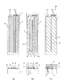
図1(a),(b),(c) は、一実施の形態におけるインクジェットプリンタヘッドの製造方法を工程順に示す図であり、それぞれ一連の工程においてヘッドチップの基板上に形成されていく状態の概略の平面図と断面図を模式的に示している。尚、これらの図には、説明の便宜上、いずれもフルカラー用のインクジェットプリンタヘッドを構成するための1個の印字ヘッド(モノクロ用インクジェットヘッドの構成と同じ)のみを示しているが、実際には後述するように、このような印字ヘッドが複数個(通常は4個)連なった形状のものが、1個のヘッドチップに形成される。また、同図(c) には36個の吐出ノズルを示しているが、実際には、設計上の方針によって異なるが64個、128個、256個等、多数の吐出ノズルが形成されるものである。
【0016】
図2(a),(b),(c) は、上段に図1(a),(b),(c) の平面図をそれぞれ一部を拡大して詳細に示しており、この図2(a),(b),(c) の中段には上段のA−A′断面矢視図(同図(a) 参照)を示し、下段には上段のB−B′断面矢視図(同図(a) 参照)示している。また、同図(a),(b),(c) の中段に示す断面図は、それぞれ図1(a),(b),(c) の下に示す断面図と同一のものである。尚、図2(a),(b),(c) には、図示する上での便宜上、64個、128個又は256個のインク吐出ノズルを、5個のインク吐出ノズルで代表させて示している。
【0017】
最初に、基本的な製造方法について説明する。先ず、工程1として、4インチ以上のシリコン基板にLSI形成処理により駆動回路とその端子を形成すると共に、厚さ1〜2μmの酸化膜(Si O2 )を形成し、次に、工程2として、薄膜形成技術を用いて、タンタル(Ta)−シリコン(Si)−酸素(O)からなる発熱抵抗体層と、Ti−W等の密着層を介在させてAuなどによる電極膜を順次積層形成する。そして、電極膜と発熱抵抗体層をフォトリソグラフィー技術によって夫々パターニングし、ストライプ状の発熱抵抗体層上の発熱部とする領域の両側に配線電極を形成する。この工程で発熱部の位置が決められる。
【0018】
図1(a) 及び図2(a) は、上記の工程1及び工程2が終了した直後の状態を示している。すなわち、ヘッドチップ1の一方の側端部近傍に駆動回路2が形成され、その上に形成された酸化膜からなる絶縁層の上に、発熱抵抗体3が形成されている。発熱抵抗体3の一方の端部に共通電極4が接続され、他方の端部と駆動回路2との間に個別配線電極5が接続されている。
【0019】
上記の発熱抵抗体3、共通電極4、及び個別配線電極5は1組となって条形状にパターン化されて、各条が発熱素子を形成し、所定の間隔で平行に並設されている。また、共通電極4には共通電極給電端子4−1が上端部に形成されており(図1(a) 参照)、これに並んで駆動回路端子2−1が形成されている(図1(a) 参照)。
【0020】
続いて、工程3として、個々の発熱抵抗体3に対応するインク加圧室及びこれらのインク加圧室にインクを供給するインク流路を形成すべく感光性ポリイミドなどの有機材料からなる隔壁部材をコーティングにより高さ20μm程度に形成し、これをフォトリソ技術によりパターン化した後に、300℃〜400℃の熱を30分〜60分加えるキュア(乾燥硬化、焼成)を行い、高さ10μm程度の上記感光性ポリイミドによる隔壁をヘッドチップ上に形成・固着させる。更に、工程4として、ウェットエッチングまたはサンドブラスト法などにより上記ヘッチップの面に溝状のインク供給路を形成し、更にこのインク供給路に連通し基板下面に開口するインク給送孔を形成する。
【0021】
この工程4では、発熱抵抗体、電極、隔壁などが形成されている表面側のインク供給路と、裏面側のインク給送孔では、形状が異なるため、表裏から別々に加工を行う。例えば表面側にインク供給路をヘッドチップの厚さ半分程度まで穿設し、裏面側からインク給送孔を穿設して表裏に貫通させる。
【0022】
図1(b) 及び図2(b) は、上述の工程3及び工程4が終了した直後の状態を示している。すなわち、溝状のインク供給路6及びインク給送孔7が形成され、インク供給路6の左側に位置する共通電極4部分と、右方の個別配線電極5が配設されている部分、及び各発熱抵抗体3と発熱抵抗体3の間に、隔壁8(シール隔壁8−1、8−2、区画隔壁8−3)が形成されている。上記の隔壁8は、個別配線電極5上のシール隔壁8−2を櫛の胴とすれば、各発熱抵抗体3と発熱抵抗体3との間に伸び出す区画隔壁8−3は櫛の歯に相当する形状をなしている。これにより、この櫛の歯状の区画隔壁8−3を仕切り壁として、その歯と歯の間の付け根部分に発熱抵抗体3が位置する微細な区画部が、発熱抵抗体3の数だけ形成される。
【0023】
この後、工程5として、ポリイミドからなる厚さ10〜30μmのフィルムのオリフィス板で、その両面又は片面に接着剤としての熱可塑性ポリイミドを極薄に例えば厚さ2〜5μmにコーテングした状態のものを、上記積層構造の最上層つまり隔壁の上に載置し、真空中で200〜250℃で加熱しながら、9.8×10⁻⁴Paの数倍の圧力で加圧し、これを数10分続けて、そのオリフィス板を固着させる。続いて真空装置又はスパッタ装置でNi、Cu又はAlなどの厚さ0.5〜1μm程度の金属膜をオリフィス板表面に蒸着する。
【0024】
更に、工程6として、オリフィス板表面の上記金属膜をパターン化して、ポリイミドを選択的にエッチングするマスクを形成し、続いて、ヘリコン波によるドライエッチングにより上記の金属膜マスクに従って吐出ノズルとして20μmφ〜40μmφの多数の孔をオリフィス板に一括形成する。
【0025】
図1(c) 及び図2(c) は、上述した工程5と工程6が終了した直後の状態を示している。すなわち、オリフィス板9が共通給電端子4−1及び駆動回路端子2−1の部分を除く全領域を覆っており、シール隔壁8−2及び区画隔壁8−3によって形成されている区画部も上を覆われて隔壁8の厚さ10μmに対応する高さの微細なインク加圧室11を形成して、その開口をインク供給路6方向に向けている。そして、これらインク加圧室11の開口とインク供給路6とを連通させる高さ10μmのインク流路12が形成されている。
【0026】
そして、オリフィス板9には、インク加圧室11の発熱抵抗体3に対向する部分に吐出ノズル13がドライエッチングによって形成されている。これにより、64個、128個又は256個の吐出ノズル13を1列に備えた多数のモノカラーインクジェットヘッド14がシリコンウェハ上に完成する。
【0027】
このようにオリフィス板9を張り付けて、その後で、下地のパターンつまり発熱抵抗体3の位置に合わせて吐出ノズル13を加工することは、予め吐出ノズル13を加工したオリフィス板9を張り合わせるよりも、遥かに生産性の高い実用性のある方法である。また、ドライエッチングによる場合は、マスクはNi、Cu、又はAlなどの金属膜を使うことで樹脂と金属膜との選択比が概略100程度得られる。したがって、20〜40μmのポリイミドフィルムをエッチングするには1μm以下の金属膜でマスクを形成することで十分である。
【0028】
ここまでが、シリコンウェハの状態で処理される。そして、最後に、工程7として、ダイシングソーなどを用いてシリコンウェハをスクライブラインに沿ってカッテングして、ヘッドチップ単位毎に個別に分割し、実装基板にダイスボンデングし端子接続して実用単位のモノカラーインクジェットヘッドが完成する。
【0029】
上記のように1列の吐出ノズル13を備えたモノカラーインクジェットヘッド14はモノクロ用インクジェットヘッドの構成であるが、通常フルカラー印字においては、減法混色の三原色であるイエロー(Y)、マゼンタ(M)、シアン(C)の3色に、文字や画像の黒部分に専用されるブラック(Bk)を加えて合計4色のインクを必要とする。したがって最低でも4列のノズル列が必要である。そして上述した製造方法によればモノカラーインクジェットヘッド14をモノリシックに4列構成とすることは可能であり、各モノカラーインクジェットヘッド14のノズル列の位置関係も今日の半導体の製造技術により正確に配置することが可能である。
【0030】
図3(a) は、上述の図1及び図2に示したヘッドチップ1、駆動回路2、駆動回路端子2−1、発熱抵抗体3、共通電極4、共通電極給電端子4−1、個別配線電極5、インク供給路6、インク供給孔7、隔壁8、オリフィス板9、インク加圧室11、インク流路12、吐出ノズル13の各部を1組としてなるヘッド素子つまりモノカラーインクジェットヘッド14をやや大きく区画したヘッドチップ20上に4列並べてフルカラーインクジェットヘッド15を構成し、これにより1個のヘッドチップ20に4列のノズル列16(16a、16b、16c、16d)を形成した状態を示す図である。また、図3(b) は、同図(a) のモノカラーインクジェットヘッド15が4列並んだ構成を分かり易く示すため、図1(a) に示した工程1〜工程2まで終了した状態のものを示している。
【0031】
この図3(a),(b) に示すように、フルカラーインクジェットヘッド15は、4個のモノカラーインクジェットヘッド14(14a、14b、14c、14d)が並んで配置され、例えばインク供給路6aからイエローインクがモノカラーインクジェットヘッド14aの個々のインク加圧室11に供給され、ノズル列16aから吐出される。また、インク供給路6bからマゼンタインクがモノカラーインクジェットヘッド14bの個々のインク加圧室11に供給され、ノズル列16bから吐出される。また、インク供給路6cからシアンインクがモノカラーインクジェットヘッド14cの個々のインク加圧室11に供給され、ノズル列16cから吐出される。そして、インク供給路6dからはブラックインクがモノカラーインクジェットヘッド14dの個々のノズル列16dに供給され、ノズル列16dから吐出される。
【0032】
ところで、本発明においては上述した基本的な製造方法における工程6において、オリフィス板9に吐出ノズル13を穿設するに際し、ジャストエッチング時点を検出するために特別の工夫が施されている。以下これについて説明する。
【0033】
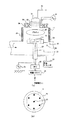
図4(a) は、ヘリコン波エッチング装置を模式的に示す図であり、同図(b) はそのウェハ固定用ステージの平面図である。同図(a) に示すように、ヘリコン波エッチング装置は、プロセスチャンバー(処理室)17を中心に、この処理室17内に突設されるウェハ固定用ステージ18を備えている。図3(a) に示したフルカラーインクジェットヘッド15が上述した工程5までを終了した状態で多数形成されているシリコンウェハ19は、図4(a) の矢印Cで示すように装置左方から搬入されて、上記のウェハ固定用ステージ18上に載置される。
【0034】
上記シリコンウェハ19は、メカチャック法(機構的に行う固定方法)又は静電チャック法(静電的に行う固定方法)で固定される。ウェハ固定用ステージ18は、支持台21上に、支持台21と一体に構成され、この支持台21を介して、例えば13.56MHzのRF(radio−frequency:高周波)バイアスが接地側交流電源22から印加される。また、このウェハ固定用ステージ18には、低温サーキュレータ23による不凍液が支持台21を介して循環している。これにより、ウェハ固定用ステージ18を循環不凍液で−10℃〜−30℃程度に冷却する。
【0035】
さらに、本発明の特徴として、ウェハ固定用ステージ18とシリコンウェハ19との間に生じている微細な隙間に、熱伝導を促進するためのHeガスなどの冷媒ガスを、流量コントーローラ24、APC(auto pressure controler )25及び支持台21とウェハ固定用ステージ18内に配設された冷媒送入路26を介し、ウェハ固定用ステージ18のウェハ支持面の中心と外周部近傍の合計7箇所に開口する冷媒吹き出し口27から送入する。
【0036】
これにより、低温サーキュレータ23によるシリコンウェハ19の冷却を促進させ、ヘリコン波ドライエッチングの際のシリコンウェハ19の温度上昇を効果的に抑制する。また、これと共に、詳しくは後述するが、冷媒ガスの流量変化から、ジャストエッチング時点の検出を行っている。
【0037】
上記の処理室17の周囲には、酸素(O2 )プラズマ28を処理室17内に閉じ込めるためのマグネット(磁石)29が配設され、処理室17の上部中央にはソースチャンバー(源流室)31が配置される。源流室31の周囲には上下二段にアンテナ32が配設され、その外側には、プラズマを封じ込めるために、内外二重にインナーコイル(内コイル)33とアウターコイル(外コイル)34が配置されている。
【0038】
この源流室31の上部には、パイプライン35が開口し、ここからプロセスガス(処理用酸素)が供給される。また、二段のアンテナ32にはソースパワーサプライ(源流電源)36から、例えば上記接地側交流電源22のサイクルに対応する13.56MHzの電圧が印加される。
【0039】
この構成により、源流室31内においてパイプライン35から供給される処理用酸素がアンテナ32によってプラズマ化され、内コイル33及び外コイル34によって処理室17に送り込まれる。この酸素プラズマ28を、処理室17内で、支持台21及びウェハ固定用ステージ18を介してシリコンウェハ19に印加されているRFバイアス電圧で吸引・加速する。
【0040】
処理室17の周囲壁面に配設されている磁石29が上記酸素プラズマ28の電子が壁面で消滅するのを防止する。これにより、酸素プラズマ28は、均一な分布となってシリコンウェハ19に降り注ぎ、オリフィス板(図2(c) のオリフィス板9参照)表面の金属膜マスクパターンで露出している部分に激突してエッチングする。処理後のプロセスガスは、図4(a) の矢印Dで示すように装置右方に排出される。
【0041】
ヘリコン波エッチングは、RIE(反応性イオンエッチング)のように電極配置が平行平板型ではないが、それと同じように、酸素プラズマ28に対してヘッドチップの電位が、酸素イオンを引き込む方向にある。これにより、工作物(シリコンウェハ19)を酸素イオンスバッタするのと同時に、ラジカル原子を利用して化学エッチングもしている。
【0042】
例えば、工作物がポリイミドの場合、その主成分は、炭素であるため、CxHy+O→CO2 ↑+H2 O↑の化学反応によるエッチングを行っている。よって、上記のヘリコン波エッチングは、スパッタ(物理的エッチング)+ラジカル反応(化学的エッチング)を使って、孔空け加工のような異方性エッチングを高い選択比で行うことができる。
【0043】
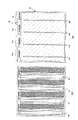
図5(a),(b),(c) は、上記のヘリコン波エッチングで孔空け加工されるシリコンウェハ19の状態を模式的に示す図である。同図(a),(b),(c) には、シリコンウェハ19に21個のヘッドチップ20を示しているが、実際には例えば150mmφ程度の大きさのシリコンウェハには90個以上のヘッドチップが形成されている。
【0044】
同図(a) は、エッチング開始前の状態であり、ヘッドチップ20の表面(オリフィス板)には、まだ吐出ノズルが孔空けされていない状態を示している。同図(b) は、エッチングが進行中の状態であり、シリコンウェハ19の中央部に在る一団のヘッドチップ20に、ノズル列16の吐出ノズルが貫通している状態を示している。そして、同図(c) は、シリコンウェハ19上の全てのヘッドチップ20の吐出ノズルが丁度貫通したジャストエッチング時点の状態を示している。
【0045】
同図(a),(b),(c) のエッチング状態図に示すように、図4(a) に示した酸素プラズマ28の分布は、均一とはいっても完全に均一なわけではなく、シリコンウェハ19の中央部の分布がやや密である。したがって、同図(b) に示すように、シリコンウェハ19の中央部の一団のヘッドチップ20の吐出ノズルが先に貫通し、その後に外周部のヘッドチップ20の吐出ノズルが貫通する。本発明においては、この全てのヘッドチップ20の吐出ノズルが丁度貫通したジャストエッチング時点を、正確に検出する。以下、これについて説明する。
【0046】
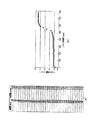
図6(a) 〜(d) は、ヘリコン波エッチングによるヘッドチップ20の孔空け加工の各段階での状態を示す図である。このヘリコン波エッチング装置による孔空け加工は、実際にはシリコンウェハ19の状態での処理、つまり、多数のフルカラーインクジェットヘッド15のヘッドチップ20に対する一括処理であるが、説明の便宜上、以下、1個の吐出ノズルを穿設する状態を拡大して示す。
【0047】
同図(a) には孔空け加工直前つまりヘリコン波エッチング装置に搬入直前のヘッドチップ20の側断面図を示し、同図(b) 〜(d) にはヘリコン波エッチング装置に搬入されたウェハ固定用ステージ18上のヘッドチップ20を示している。尚、同図(a) 〜(d) には、図1〜図3に示した構成と同一の構成部分には図1〜図3と同一の番号を付して示している。また、本例では、オリフィス板9として、ポリイミドのフィルム9aの両面に熱可塑性ポリイミド9bを塗布した形態のものを用いている。勿論、熱可塑性ポリイミド9bを下面にのみ塗布したものを用いても良い。
【0048】
また、この図6(a) 〜(d) には、図1〜図3では図示を省略した金属膜マスクパターン37も示しており、この金属膜マスクパターン37には発熱抵抗体3に対向する部分に吐出ノズル用の孔37−1が形成され、ここにオリフィス板9の表面が露出している。
【0049】
このヘッドチップ20が、ヘリコン波エッチング装置に搬入されて、図6(b) に示すように、ウェハ固定用ステージ18上に固定され、ヘリコン波エッチングが開始されると、ヘッドチップ20の上方に形成された酸素プラズマ28が金属膜マスクパターン37に吹き付けられ、ヘッドチップ20の下面とウェハ固定用ステージ18との間隙に冷媒ガス38が送入される。
【0050】
そして、図6(c) に示すように、エッチングが進行し吐出ノズル13の孔空けが進行する。この間、上記の冷媒ガス38は、ウェハ固定用ステージ18の冷媒吹き出し口27より供給され、ヘッドチップ20裏面との間隙を吹き抜けては外周より排出され、不図示のポンプに吸い込まれる。また、この間、冷媒ガス38の圧力が一定になるように、その流量が、流量コントローラ24及びAPC25によって制御される。
【0051】
図6(c) に示す未だ吐出ノズル13が貫通していないハーフエッチング時は、冷媒ガス38はヘッドチップ20の外周部から流出する分だけ補給されて、その流量は一定である。
【0052】
やがて、図6(d) に示すように、吐出ノズル13が貫通し、図5(b) に示したうようにシリコンウェハ19の中央部の一団のヘッドチップ20から図5(c) に示した全ヘッドチップ20の吐出ノズルが貫通するジャストエッチング時点まで、貫通した吐出ノズル13を吹き抜けて流出する冷媒ガス38の量が、貫通した吐出ノズル13の数に応じて増加し、その圧力を一定に保つべく、より多くの冷媒ガス38が供給される。
【0053】
そして、ジャストエッチング時点からオーバーエッチング時は、冷媒ガス38の流出経路に変化はなく、したがって、流量は増加したままの一定量に安定する。尚、オーバーエッチング時に冷媒ガス38が吐出ノズル13を通じて流出するが、冷媒ガス38はHe等の不活性ガスであるのでエッチングの仕上げに悪影響を及ぼすことはない。
【0054】
図7(a) は、上記冷媒ガス38の時間毎の流量を不図示の流量変化検出回路で実測した結果を示す図表であり、同図(b) はその値を点描したグラフである。同図(a) 左欄に処理時間を秒(sec)単位で示し、右欄に冷媒ガス(Heガス)38の時間当たり流量を示している。時間当り流量の単位は、標準つまりスタンダードの状態(25℃、1気圧)で毎分当り立方センチメートルの流量(sccm)で示している。また、同図(b) は、横軸に上記の処理時間を示し、縦軸に上記の流量を示している。
【0055】
図7(a),(b) に示すように、時間が0secから500secまでは、図5(a) に示した状態で、いずれの吐出ノズル13も未貫通であり、流量は約9.4sccmで安定している。
【0056】
そして、時間が500secから600secまでは、図5(b) に示した吐出ノズル13が一部貫通し始めた状態であり、流量は9.4〜9.7sccmまで急激に変化し、時間が600sec以降は、図5(c) に示した全吐出ノズル13が貫通した状態であり、流量は約9.7sccmで安定している。
【0057】
本発明は、上記のヘリコン波エッチングにおいて、冷媒ガス38の増量変化した後の流量の安定した状態(図7(a),(b) に示す例では時間600sec以降)を検出する。この流量の安定した状態を検出している期間は実はオーバーエッチング期間である。本発明は、上記の流量安定状態の検出に基づき、その流量安定状態の始まりの時点(図7(a),(b) に示す例では時間600secの時点)を、ジャストエッチング時点とする。
【0058】
そして、このジャストエッチング時点から所定の期間をオーバーエッチング期間として、このオーバーエッチングにより、吐出ノズル13内に発生したエッチング残渣を除去して、適正な吐出ノズル13を形成する。
【0059】
このオーバーエッチングにおいては、上記のように、シリコンウェハ19の中心部のヘッドチップ20は、外周部のヘッドチップ20よりも100sec程度早く貫通しているため、早く貫通した吐出ノズル13直下の発熱抵抗体3は、早く貫通した分だけ、過剰にオーバーエッチングされることになる。
【0060】
このように、オーバーエッチングでは、シリコンウェハ19の中心部と外周部でエッチングレートが異なるため、シリコンウェハ19上のヘッドチップ20には、中心部と外周部とで発熱抵抗体3の抵抗率にバラツキが発生する。
【0061】
この発熱抵抗体3の抵抗率のバラツキの程度は、発熱抵抗体3の構成を4元系のTa−Si−O−Nとし、オリフィス板9のシート抵抗を120Ω/□とし、酸素プラズマによるへリコン波エッチングレートを15nm/minとしたとき、中心部のヘッドチップ20の発熱抵抗体3の膜厚は475nm、外周部のヘッドチップ20の発熱抵抗体3の膜厚は500nmであった。すなわち、中心部のヘッドチップ20の発熱抵抗体3の方が、外周部のヘッドチップ20の発熱抵抗体3よりも時間で100sec、厚さで25nmだけ過剰にオーバーエッチングされたことになる。
【0062】
上記の膜厚475nmの発熱抵抗体3の抵抗率は5.7mΩ・cm、膜厚500nmの発熱抵抗体3の抵抗率は6.0mΩ・cmである。このバラツキの程度は、測定された上記抵抗率の最大値をMAX、最小値をMINとして、式「{(MAX−MIN)/(MAX+MIN)}×100」により計算すると2.56%であり、品質上問題がないと判断される範囲である。
【0063】
尚、上記のインクジェットヘッドの製造工程では、ヘッドチップに、電極、発熱抵抗体、隔壁、インク供給路、インク供給孔等から成るヘッド部と駆動回路とを一体で構成する例を示したが、インクジェットヘッドの部分だけをシリコン基板またはガラス基板などの基板に形成しても良く、この場合も、上記と全く同様に処理してジャストエッチング時点を容易に検出することができる。
【0064】
また、本発明の貫通孔加工法は、吐出ノズルに限定されるものではなく、例えばインク供給路又はインク供給孔等の穿設・貫通加工は勿論、インクジェットヘッド以外の工作物のドライエッチングによる孔空け等にも広く適用できる。
【0065】
更に、本発明は、上述した実施形態のように貫通孔の一部をドライエッチングにより穿設する場合に限らず、貫通孔をその全長に亙りドライエッチングにより穿設する場合にも、好適に適用できることは勿論である。
【0066】
【発明の効果】
以上詳細に説明したように、本発明によれば、ドライエッチングによる貫通孔加工において、工作物を冷却するための冷媒ガスの流量の変化を読み取ることにより、孔が貫通したジャストエッチング時点を容易且つ正確に把握できるので、これにより、過度なオーバーエッチングによる工作物の損傷を防止することができると共に、オーバーエッチングの時間を必要最小限に短縮することが可能となる。
【0067】
また、冷媒ガスの流量の変化を読み取ってジャストエッチング時点を検出するので、流量コントーローラ24とAPC25及び流量変化検出回路を付加するだけでよく、装置が極めて簡便で安価である。
【0068】
また、不活性の冷媒ガスを用いることにより、エッチング系を乱すことがなく、したがって、貫通孔加工の加工対象物としての材料には限定されることがなく、精度の良い且つ使い勝手のよい貫通孔加工方法を提供することが可能となる。
【0069】
また、冷媒ガスの流量変化を読み取ることによるジャストエッチング時点の検出であるので、貫通孔加工対象物の表面の凹凸等からの影響を受けることがなく、したがって、制約の少ない貫通孔加工方法を提供することが可能となる。
【0070】
また、冷媒ガス流量の変化を短時間毎に読み取って、流量の急変から安定化の状態になるジャストエッチング時点を検出することにより、検出の感度が極めて高く、ジャストエッチング時点検出の精度の良い貫通孔加工方法を提供することが可能となる。
【図面の簡単な説明】
【図1】(a),(b),(c) は一実施の形態におけるインクジェットプリンタヘッドの製造方法を工程順に示す図である。
【図2】(a),(b),(c) の上段は図1(a),(b),(c) の平面図の一部拡大図、中段は上段のA−A′断面矢視図、下段は上段のB−B′断面矢視図である。
【図3】(a) は一実施の形態におけるフルカラーインクジェットヘッドの平面図、(b) はその製造工程2まで終了した状態のものを示す図である。
【図4】(a) は一実施の形態におけるヘリコン波エッチング装置を模式的に示す図、(b) はそのウェハ固定用ステージの平面図である。
【図5】(a),(b),(c) はのヘリコン波エッチングで孔空け加工されるシリコンウェハの状態を模式的に示す図である。
【図6】(a) 〜(d) はヘリコン波エッチングによるヘッドチップの孔空け加工の状態を示す図である。
【図7】(a) は冷媒ガスの流量の実測結果を示す図表、(b) はその値を点描したグラフである。
【符号の説明】
1 ヘッドチップ
2 駆動回路
2−1 駆動回路端子
3 発熱抵抗体
4 共通電極
4−1 共通電極給電端子
5 個別配線電極
6(6a、6b、6c、6d) インク供給路
7 インク給送孔
8 隔壁
8−1、8−2 シール隔壁
8−3 区画隔壁
9 オリフィス板
11 インク加圧室
12 インク流路
13 吐出ノズル
14(14a、14b、14c、14d) モノカラーインクジェットヘッド
15 フルカラーインクジェットヘッド
16(16a、16b、16c、16d) ノズル列
17 プロセスチャンバー(処理室)
18 ウェハ固定用ステージ
19 シリコンウェハ
20 ヘッドチップ
21 支持台
22 接地側交流電源
23 低温サーキュレータ
24 流量コントーローラ
25 APC(auto pressure controler)
26 冷媒送入路
27 冷媒吹き出し口
28 酸素(O2 )プラズマ
29 マグネット(磁石)
31 ソースチャンバー(源流室)
32 アンテナ
33 インナーコイル(内コイル)
34 アウターコイル(外コイル)
35 パイプライン
36 ソースパワーサプライ(源流電源)
37 金属膜マスクパターン
37−1 孔
38 冷媒ガス[0001]
TECHNICAL FIELD OF THE INVENTION
The present invention relates to a through-hole processing method capable of easily and accurately detecting a point in time when a through-hole is formed by dry etching.
[0002]
[Prior art]
Conventionally, for example, when a through-hole such as a discharge nozzle for discharging ink of an ink jet head is formed by dry etching, even when the discharge nozzle penetrates, that is, after the just etching time, the deburring of the discharge nozzle is performed. In order to perform finishing, a so-called over-etching period in which dry etching is continued for a predetermined time is provided.
[0003]
However, if the time for performing the over-etching is longer than necessary, a problem occurs in that another portion of the processing target on which the discharge nozzle is to be formed is damaged.
[0004]
Particularly, in a method of manufacturing an ink jet head in which a large number of discharge nozzles on a silicon wafer on which a plurality of head chips are formed are collectively formed, it is difficult to form all the discharge nozzles at the same time. If the detection of the just-etching time when the nozzle penetrates is delayed, excessive over-etching by that amount increases the amount of the heat-generating resistor corresponding to the discharge nozzle that has penetrated first. In this case, the variation in the resistivity of each heating resistor corresponding to each ejection nozzle becomes large, and the quality of the ink jet head itself is further varied.
[0005]
Therefore, over-etching must be performed exactly for a predetermined time from the time of the just-etching. In order to accurately perform the over-etching for a predetermined time, it is necessary to accurately detect the just-etching time itself.
[0006]
Conventionally, there are various methods for detecting the just etching time, such as emission spectroscopy, reflected light analysis, laser interferometry, gas analysis, impedance measurement, pressure measurement, and etching rate measurement. Used.
[0007]
[Problems to be solved by the invention]
However, the above-mentioned emission spectroscopy has a problem that detection may not be possible if the detection area is small, and that the measuring instrument is extremely expensive, for example, 4 million yen to 7 million yen. . In addition, the reflected light analysis method and the laser interferometry method have a disadvantage that not only the material that can be detected is limited, but also the accuracy is lowered because the material is easily affected by irregularities on the surface of the object to be processed. In addition, the gas analysis method has problems that not only the apparatus is complicated, but also the types of detectable materials are small and the detection sensitivity is low.
[0008]
Further, the impedance measurement method has a problem that it is difficult to adjust the impedance measurement method because it may be affected by the automatic control system. Further, the pressure measurement method has problems that it cannot coexist with an automatic pressure adjustment mechanism and that the detection sensitivity is low. In addition, the etching rate measurement method is a method of calculating an etching rate and determining the end point of etching by time management, but it is inaccurate because it changes depending on the state of the apparatus and the work condition of the workpiece. Had.
[0009]
As described above, there are various methods for detecting the point of just etching, but each has its own disadvantages, and there is no versatile one that can be applied to any workpiece. It is.
[0010]
An object of the present invention is to provide a through-hole processing method that can easily and accurately detect a penetration point of a through-hole when a through-hole is formed by dry etching, that is, a just-etching point, in view of the above conventional circumstances. is there.
[0011]
[Means for Solving the Problems]
The through-hole processing method of the present invention is a through-hole processing method in which at least a part of the through-hole that penetrates from the back surface to the front side while being cooled by a cooling medium gas that causes the back surface of the processing object to flow at a constant pressure is processed by dry etching. In the hole forming method, the point of the just etching when the through-hole penetrates by the processing by the dry etching is detected from the change of the flow rate per hour of the cooling medium gas.
[0012]
The dry etching is preferably, for example, a helicon wave dry etching.
The object to be processed is, for example, an inkjet printer head that performs recording by applying pressure to ink and ejecting the ink from a discharge nozzle to a recording medium. A configuration including the discharge nozzle may be employed.
[0013]
In this case, for example, it is preferable that a plurality of the discharge nozzles are provided, and a point in time when all the processing of the discharge nozzles is completed is set as a just etching point.
[0014]
Preferably, the just-etching time is a time point at which the cooling medium gas starts to stabilize at a constant level after the flow rate per hour of the cooling medium gas sharply increases. Further, for example, if the over-etching is set so as to end the dry etching related to the etching after a predetermined time from the time of the just-etching, the over-etching time can be set to a necessary minimum.
[0015]
BEST MODE FOR CARRYING OUT THE INVENTION
Hereinafter, embodiments of the present invention will be described with reference to the drawings.
FIGS. 1A, 1B, and 1C are diagrams showing a method of manufacturing an ink jet printer head according to an embodiment in the order of steps, and show a state in which a head chip is formed on a substrate in a series of steps. FIG. 1 schematically shows a schematic plan view and a cross-sectional view. In these figures, for convenience of explanation, only one print head (the same as the configuration of the monochrome inkjet head) for configuring the full-color inkjet printer head is shown, but in actuality, As described below, a plurality of (normally four) such print heads are formed in one head chip. FIG. 3 (c) shows 36 discharge nozzles. Actually, a large number of discharge nozzles such as 64, 128 and 256 are formed depending on the design policy. It is.
[0016]
2 (a), (b) and (c) show the plan views of FIGS. 1 (a), (b) and (c) in a partially enlarged manner in the upper part, respectively. The middle section of (a), (b), (c) shows an AA 'cross-sectional view of the upper section (see FIG. 3 (a)), and the lower section shows an BB' cross-sectional view of the upper section ( FIG. 1A, 1B, and 1C are the same as the cross-sectional views shown below FIGS. 1A, 1B, and 1C, respectively. 2 (a), 2 (b) and 2 (c), for convenience of illustration, 64, 128 or 256 ink ejection nozzles are represented by five ink ejection nozzles. ing.
[0017]
First, a basic manufacturing method will be described. First, as a
[0018]
FIG. 1A and FIG. 2A show a state immediately after the
[0019]
The
[0020]
Subsequently, as a
[0021]
In
[0022]
FIG. 1B and FIG. 2B show a state immediately after
[0023]
Thereafter, as
[0024]
Further, as a
[0025]
FIG. 1C and FIG. 2C show a state immediately after
[0026]
In the
[0027]
Bonding the
[0028]
The processing up to this point is performed in the state of a silicon wafer. Finally, as step 7, the silicon wafer is cut along a scribe line using a dicing saw or the like, divided into individual head chip units, die-bonded to a mounting substrate, and connected to terminals for practical use. Is completed.
[0029]
As described above, the mono-color ink-jet head 14 having the one row of
[0030]
FIG. 3A shows the
[0031]
As shown in FIGS. 3A and 3B, the full-
[0032]
By the way, in the present invention, in the
[0033]
FIG. 4A is a diagram schematically showing a helicon wave etching apparatus, and FIG. 4B is a plan view of the wafer fixing stage. As shown in FIG. 1A, the helicon wave etching apparatus includes a process chamber (processing chamber) 17 and a
[0034]
The
[0035]
Further, as a feature of the present invention, a refrigerant gas such as He gas for promoting heat conduction is supplied to the minute gap generated between the
[0036]
Thereby, the cooling of the
[0037]
Oxygen (O 2 A) A magnet (magnet) 29 for confining the
[0038]
A
[0039]
With this configuration, the processing oxygen supplied from the
[0040]
A
[0041]
In the helicon wave etching, the electrode arrangement is not parallel plate type as in RIE (reactive ion etching), but similarly, the potential of the head chip is in the direction of drawing oxygen ions with respect to the
[0042]
For example, when the workpiece is polyimide, its main component is carbon, so that CxHy + O → CO 2 ↑ + H 2 Etching is performed by a chemical reaction of O ↑. Therefore, the above-mentioned helicon wave etching can perform anisotropic etching such as a hole forming process with a high selectivity by using sputter (physical etching) + radical reaction (chemical etching).
[0043]
FIGS. 5A, 5B, and 5C are diagrams schematically showing a state of the
[0044]
FIG. 5A shows a state before the start of etching, in which a discharge nozzle has not yet been formed on the surface (orifice plate) of the
[0045]
As shown in the etching state diagrams of FIGS. 4A, 4B and 4C, the distribution of the
[0046]
6 (a) to 6 (d) are views showing states at each stage of drilling a hole in the
[0047]
FIG. 3A is a side sectional view of the
[0048]
FIGS. 6A to 6D also show a metal
[0049]
The
[0050]
Then, as shown in FIG. 6C, the etching proceeds, and the opening of the
[0051]
At the time of the half etching in which the
[0052]
Eventually, as shown in FIG. 6 (d), the
[0053]
Then, from the time of the just etching to the time of the over-etching, there is no change in the outflow path of the
[0054]
FIG. 7A is a table showing the results of actual measurement of the flow rate of the
[0055]
As shown in FIGS. 7 (a) and 7 (b), from time 0 sec to 500 sec, none of the discharge nozzles 13 is penetrated in the state shown in FIG. 5 (a), and the flow rate is about 9.4 sccm. And stable.
[0056]
Then, from 500 sec to 600 sec, the
[0057]
According to the present invention, in the helicon wave etching, a state in which the flow rate is stable after the increase in the amount of the
[0058]
Then, by setting a predetermined period from the time of the just etching as an over-etching period, an etching residue generated in the
[0059]
In this over-etching, as described above, since the
[0060]
As described above, in the over-etching, since the etching rate is different between the central portion and the outer peripheral portion of the
[0061]
The degree of variation in the resistivity of the
[0062]
The
[0063]
In the above-described inkjet head manufacturing process, an example is shown in which the head chip, the head unit including the electrodes, the heating resistors, the partition walls, the ink supply paths, the ink supply holes, and the drive circuit are integrally formed. Only the portion of the inkjet head may be formed on a substrate such as a silicon substrate or a glass substrate. In this case as well, the point of just etching can be easily detected by performing the processing exactly as described above.
[0064]
Further, the method of forming a through hole according to the present invention is not limited to the discharge nozzle. For example, a hole formed by dry etching of a workpiece other than an ink jet head is not limited to drilling and penetrating an ink supply path or an ink supply hole. It can be widely applied to emptying and the like.
[0065]
Further, the present invention is preferably applied not only to the case where a part of the through hole is formed by dry etching as in the above-described embodiment, but also to the case where the through hole is formed by dry etching over the entire length. Of course, you can.
[0066]
【The invention's effect】
As described above in detail, according to the present invention, in the processing of a through hole by dry etching, by reading the change in the flow rate of the refrigerant gas for cooling the workpiece, it is easy and easy to determine the point of just etching when the hole has penetrated. Since it can be accurately grasped, it is possible to prevent the workpiece from being damaged due to excessive overetching, and it is possible to shorten the overetching time to a necessary minimum.
[0067]
Further, since the change in the flow rate of the refrigerant gas is read to detect the point of just etching, it is only necessary to add the
[0068]
In addition, by using an inert refrigerant gas, the etching system is not disturbed, and therefore, the material to be processed in the through hole processing is not limited to the material, and the accurate and easy-to-use through hole is used. It is possible to provide a processing method.
[0069]
Also, since the just etching is detected by reading the change in the flow rate of the refrigerant gas, the method is not affected by the unevenness of the surface of the through-hole processing object or the like, thus providing a through-hole processing method with less restrictions. It is possible to do.
[0070]
In addition, by reading the change in the flow rate of the refrigerant gas every short time and detecting the just-etching time point at which the flow rate changes suddenly to a stable state, the detection sensitivity is extremely high, and the penetration of the just-etching time point with high accuracy is detected. It is possible to provide a hole drilling method.
[Brief description of the drawings]
FIGS. 1A, 1B, and 1C are diagrams showing a method of manufacturing an ink jet printer head according to an embodiment in the order of steps.
2 (a), 2 (b) and 2 (c) are partially enlarged views of the plan views of FIGS. 1 (a), 1 (b) and 1 (c). The lower part is a sectional view taken along the line BB ′ of the upper part.
FIG. 3A is a plan view of a full-color inkjet head according to one embodiment, and FIG. 3B is a view showing a state where the
FIG. 4A is a diagram schematically showing a helicon wave etching apparatus according to an embodiment, and FIG. 4B is a plan view of a wafer fixing stage.
FIGS. 5A, 5B, and 5C are diagrams schematically showing a state of a silicon wafer to be drilled by helicon wave etching of FIGS.
FIGS. 6 (a) to 6 (d) are views showing a state in which a hole is formed in a head chip by helicon wave etching.
7A is a table showing the results of actual measurement of the flow rate of the refrigerant gas, and FIG. 7B is a graph in which the values are plotted.
[Explanation of symbols]
1 Head chip
2 Drive circuit
2-1 Drive circuit terminal
3 Heating resistor
4 Common electrode
4-1 Common electrode power supply terminal
5 Individual wiring electrodes
6 (6a, 6b, 6c, 6d) Ink supply path
7 Ink feed hole
8 Partition wall
8-1, 8-2 Seal partition
8-3 Partition wall
9 Orifice plate
11 Ink pressurizing chamber
12 Ink channel
13 Discharge nozzle
14 (14a, 14b, 14c, 14d) Mono-color inkjet head
15 Full-color inkjet head
16 (16a, 16b, 16c, 16d) Nozzle row
17 Process chamber (processing room)
18 Stage for Fixing Wafer
19 Silicon wafer
20 head chips
21 Support
22. Ground side AC power supply
23 Low temperature circulator
24 Flow controller
25 APC (auto pressure controller)
26 Refrigerant inlet
27 Refrigerant outlet
28 Oxygen (O 2 )plasma
29 Magnet
31 Source chamber (head flow chamber)
32 antenna
33 Inner coil (inner coil)
34 outer coil (outer coil)
35 pipeline
36 Source power supply (source power supply)
37 Metal film mask pattern
37-1 hole
38 Refrigerant gas
Claims (6)
前記冷却媒体ガスの時間当たり流量の変化から、前記ドライエッチングによる加工により前記貫通孔が貫通したジャストエッチング時点を検出することを特徴とする貫通孔加工方法。A through-hole processing method of processing at least a part of the through-hole that penetrates from the back surface to the front side by dry etching while being cooled by a cooling medium gas that causes the back surface of the processing object to flow at a constant pressure,
A method of processing a through-hole, wherein a time point of the just etching when the through-hole is penetrated by the processing by the dry etching is detected from a change in a flow rate per hour of the cooling medium gas.
Priority Applications (1)
| Application Number | Priority Date | Filing Date | Title |
|---|---|---|---|
| JP29313199A JP3598397B2 (en) | 1999-10-15 | 1999-10-15 | Through hole processing method |
Applications Claiming Priority (1)
| Application Number | Priority Date | Filing Date | Title |
|---|---|---|---|
| JP29313199A JP3598397B2 (en) | 1999-10-15 | 1999-10-15 | Through hole processing method |
Publications (2)
| Publication Number | Publication Date |
|---|---|
| JP2001115282A JP2001115282A (en) | 2001-04-24 |
| JP3598397B2 true JP3598397B2 (en) | 2004-12-08 |
Family
ID=17790826
Family Applications (1)
| Application Number | Title | Priority Date | Filing Date |
|---|---|---|---|
| JP29313199A Expired - Fee Related JP3598397B2 (en) | 1999-10-15 | 1999-10-15 | Through hole processing method |
Country Status (1)
| Country | Link |
|---|---|
| JP (1) | JP3598397B2 (en) |
Families Citing this family (3)
| Publication number | Priority date | Publication date | Assignee | Title |
|---|---|---|---|---|
| KR100724205B1 (en) * | 2002-12-30 | 2007-05-31 | 동부일렉트로닉스 주식회사 | Helium gas supply system of etching equipment |
| CN110161589B (en) * | 2019-06-24 | 2024-04-05 | 上海华瑞气雾剂有限公司 | Hole measuring device |
| WO2025126489A1 (en) * | 2023-12-15 | 2025-06-19 | 日本電信電話株式会社 | Optical waveguide and production method for same |
Family Cites Families (4)
| Publication number | Priority date | Publication date | Assignee | Title |
|---|---|---|---|---|
| JPS52134197A (en) * | 1976-05-06 | 1977-11-10 | Harashin Kougiyou Yuugen | Method of providing patters to stone material |
| JPH01274427A (en) * | 1988-04-27 | 1989-11-02 | Hitachi Ltd | Sample backside gas pressure control device |
| JPH04306826A (en) * | 1991-04-03 | 1992-10-29 | Nikon Corp | ion milling equipment |
| JPH09232281A (en) * | 1996-02-26 | 1997-09-05 | Sony Corp | Dry etching method |
-
1999
- 1999-10-15 JP JP29313199A patent/JP3598397B2/en not_active Expired - Fee Related
Also Published As
| Publication number | Publication date |
|---|---|
| JP2001115282A (en) | 2001-04-24 |
Similar Documents
| Publication | Publication Date | Title |
|---|---|---|
| EP0609011B1 (en) | Method for manufacturing a thermal ink-jet print head | |
| KR100537522B1 (en) | Piezoelectric type inkjet printhead and manufacturing method of nozzle plate | |
| JPH021311A (en) | Manufacture of thin-film resistor device and ink-jet printing head | |
| JPS63116857A (en) | Liquid jet recording head | |
| US7048359B2 (en) | Ink-jet printhead and method for producing the same | |
| US9096063B2 (en) | Liquid ejection head and method of manufacturing same | |
| EP1075390B1 (en) | Method of manufacturing ink-jet printer head | |
| US6926386B2 (en) | Inkjet printer head and method of fabricating the same | |
| JP3598397B2 (en) | Through hole processing method | |
| JP2011056906A (en) | Method of manufacturing liquid discharge head | |
| US6454379B1 (en) | Liquid discharge head and liquid discharge apparatus that uses the liquid discharge head, and discharge volume correction method for the liquid discharge head | |
| US20030034326A1 (en) | Method for producing liquid discharge head | |
| JP2001162803A (en) | Monolithic inkjet printer head | |
| KR101118431B1 (en) | Substrate and method of forming substrate for fluid ejection device | |
| CN100415521C (en) | Liquid ejecting head, liquid ejecting apparatus, and method of manufacturing liquid ejecting head | |
| JP3692842B2 (en) | Inkjet printer head manufacturing method | |
| JP2002075964A (en) | Anisotropic etching method | |
| JP3045793B2 (en) | Inkjet head, substrate for inkjet head, inkjet apparatus, and method for manufacturing substrate for inkjet head | |
| JP2004209708A (en) | INK JET PRINT HEAD, METHOD OF MANUFACTURING THE SAME, AND SUBSTRATE FOR INK JET PRINT HEAD USED FOR MANUFACTURING THE SAME | |
| JP2005144782A (en) | A method for manufacturing an inkjet recording head. | |
| US7097280B2 (en) | Printheads having improved heater chip construction | |
| JPH06183005A (en) | Ink jet recording head, manufacturing method thereof, and recording apparatus using the head | |
| JPH08132629A (en) | Ink jet head and production thereof | |
| JPH07137261A (en) | THERMAL INKJET RECORDING HEAD, ITS MANUFACTURING METHOD, AND RECORDING DEVICE HAVING THE SAME | |
| JP2004076047A (en) | Thin film manufacturing method and manufacturing apparatus |
Legal Events
| Date | Code | Title | Description |
|---|---|---|---|
| A977 | Report on retrieval |
Free format text: JAPANESE INTERMEDIATE CODE: A971007 Effective date: 20040810 |
|
| TRDD | Decision of grant or rejection written | ||
| A01 | Written decision to grant a patent or to grant a registration (utility model) |
Free format text: JAPANESE INTERMEDIATE CODE: A01 Effective date: 20040817 |
|
| A61 | First payment of annual fees (during grant procedure) |
Free format text: JAPANESE INTERMEDIATE CODE: A61 Effective date: 20040830 |
|
| R150 | Certificate of patent or registration of utility model |
Free format text: JAPANESE INTERMEDIATE CODE: R150 |
|
| FPAY | Renewal fee payment (event date is renewal date of database) |
Free format text: PAYMENT UNTIL: 20070924 Year of fee payment: 3 |
|
| FPAY | Renewal fee payment (event date is renewal date of database) |
Free format text: PAYMENT UNTIL: 20080924 Year of fee payment: 4 |
|
| FPAY | Renewal fee payment (event date is renewal date of database) |
Free format text: PAYMENT UNTIL: 20090924 Year of fee payment: 5 |
|
| FPAY | Renewal fee payment (event date is renewal date of database) |
Free format text: PAYMENT UNTIL: 20100924 Year of fee payment: 6 |
|
| FPAY | Renewal fee payment (event date is renewal date of database) |
Free format text: PAYMENT UNTIL: 20100924 Year of fee payment: 6 |
|
| FPAY | Renewal fee payment (event date is renewal date of database) |
Free format text: PAYMENT UNTIL: 20110924 Year of fee payment: 7 |
|
| FPAY | Renewal fee payment (event date is renewal date of database) |
Free format text: PAYMENT UNTIL: 20120924 Year of fee payment: 8 |
|
| FPAY | Renewal fee payment (event date is renewal date of database) |
Free format text: PAYMENT UNTIL: 20130924 Year of fee payment: 9 |
|
| LAPS | Cancellation because of no payment of annual fees |