JP3596543B2 - Stamper, method of manufacturing the same, optical disk and blanks - Google Patents
Stamper, method of manufacturing the same, optical disk and blanks Download PDFInfo
- Publication number
- JP3596543B2 JP3596543B2 JP2002306937A JP2002306937A JP3596543B2 JP 3596543 B2 JP3596543 B2 JP 3596543B2 JP 2002306937 A JP2002306937 A JP 2002306937A JP 2002306937 A JP2002306937 A JP 2002306937A JP 3596543 B2 JP3596543 B2 JP 3596543B2
- Authority
- JP
- Japan
- Prior art keywords
- photoresist
- photoresist layer
- stamper
- layer
- substance
- Prior art date
- Legal status (The legal status is an assumption and is not a legal conclusion. Google has not performed a legal analysis and makes no representation as to the accuracy of the status listed.)
- Expired - Fee Related
Links
Images


Description
【0001】
【発明の属する技術分野】
本発明は、光ディスクと、光ディスクを成形する時に用いられるスタンパーとその製造方法及び光ディスク並びにブランクスに関するものである。
【0002】
【従来の技術】
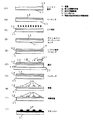
従来、光ディスクを製作するためのスタンパーはマスタリングといわれる工程で製作されていた。この工法は一般にフォトリソグラフィーといわれる技術を用い、ガラス盤上に信号に対応したフォトレジストの凹凸のパターンを形成することから始まる。ガラス盤上のポジ型フォトレジスト層に、記録すべき信号に対応して強度変調されたレーザビームを螺旋状に露光し、現像することによって、レジストの窪み(ピット)をトラック状に形成するのである。その後、表面に導電性膜を形成し、その上に電鋳によりニッケルの厚膜を形成する。その厚膜はおよそ0.3mmほどであり、それを元のガラス盤から剥がしてスタンパーにするのである。このニッケル盤にはフォトレジストのピットが転写された突起(バンプ)が螺旋状に形成されている。これを射出成形することにより情報を含んだピット列を有する光ディスクが出来るのである。
【0003】
このスタンパーを作る工程は10以上の工程を含み、製作のための多くの時間とコストがかかる。また工程が多いために塵埃や人為的ミスなどによる欠陥も多く、歩留まりを低下させていた。
【0004】
近年、このような多くの工程を要せず、より少ない工程でスタンパーを作る試みがなされている。特許公報第2765421号には基板の上に架橋性無機物または架橋性有機物層を設け、記録信号で強度変調されたレーザビームを照射し、現像することにより基板上に信号パターンに対応した突起部を設け、さらに加熱により突起部を強固なものにした後、その基板を直接スタンパーとする工法が示されている。図5に従って従来例を説明する。図5(A)にはニッケル基板1と架橋性無機物または架橋性有機物層が2で示されている。図5(B)は信号変調されたレーザビーム3が記録レンズ4で絞られて架橋性物質2を露光するところを示す。図5(C)にはレーザ露光の潜像としての露光部が局所的に加熱されて架橋し、5のマークを形成しているところを示す。これを現像すると未露光部は溶解し、露光部のみ6として残る。これら架橋性物質2はいわゆるネガ型レジストの作用をする。図5(D)はその状態の基板を表している。これを300℃の高温でハードベーキング処理をすると6のマーク部は架橋が促進され強固になる。このように作られた基板をそのままスタンパーにするのである。その為このスタンパーはダイレクトスタンパーと称されている。
【0005】
また、特開平7−326077号公報には基板上にフォトレジスト(架橋性物質)の突起を形成し、高温加熱により架橋を促進した後、直接それをダイレクトスタンパーとして用いる方法が示されている。この特許が特許公報第2765421号の方法と異なるのは、フォトレジストを選択的に露光し酸を発生させる。その後全体を加熱することにより酸が触媒となり露光部のみに架橋を起こさせる。次に全体を露光すると、前回未露光であったところに酸が生成され、かつそこは架橋されていないので現像液で溶解され、最初に露光されたところが突起として残るのである。
【0006】
【特許文献1】
特許公報第2765421号
【特許文献2】
特開平7−326077号公報
【0007】
【発明が解決しようとする課題】
しかしながら、従来のダイレクトスタンパーは何れもニッケル基板の上に有機または無機のフォトレジスト(架橋性物質)の突起を直接形成したものである。このため、高温ベークによりフォトレジストの硬度は硬くなっているが、本来フォトレジストと金属との接着力は強くない。またDVDの場合、フォトレジストの突起の幅は0.3μm、長さは最短のもので0.4μmと接着面積は非常に小さい。
【0008】
このダイレクトスタンパーは成形機の金型に取り付けられ、鏡面金型とキャビティを形成する。その中に高温の樹脂が高圧で注入される。その時、高圧の樹脂はフォトレジスト突起を引き剥がす作用を起こす。
【0009】
また、一般に金型の温度は100℃前後に設定されているが、注入される樹脂は約300℃以上の高温である。樹脂の射出によってダイレクトスタンパー表面温度は上昇し、成形ディスク(光ディスク)の取り出しによって元の温度に戻るという熱膨張と収縮が繰り返される。ニッケルのような金属とフォトレジストの熱膨張係数には大きな違いがあり、その熱膨張の違いによる応力が繰り返しフォトレジスト突起に作用し、ついには基板から剥離させる。
【0010】
従来のダイレクトスタンパーでDVD(光ディスク)などのディスクを成形すると約5000〜10000ショット位の成形でフォトレジスト突起の欠落によるDVDの再生信号エラーが許容限界値に達する。DVDでは、欠陥によるエラーはPIエラーと呼ばれ、エラー訂正前において8ECCブロックの中で280以下と決められている。そのため、従来のダイレクトスタンパーを用いたDVD(光ディスク)などのディスクの成形では、約5000〜10000ショット以上の成形をすることが出来なかった。
【0011】
【課題を解決するための手段】
上記課題を解決するために、本発明の第1のスタンパーの製造方法は、基盤上に架橋性物質の層を形成し、前記架橋性物質の層に第1の架橋反応を施した後、前記架橋性物質の層の上にフォトレジストの層を形成し、その後、前記フォトレジストの層に記録すべき信号によって変調されたレーザビームの露光および現像を行った後、前記架橋性物質および前記フォトレジストの各層に更に第2の架橋反応を施して、前記架橋性物質の層と前記フォトレジストの層とを架橋結合させたことを特徴とする。
【0012】
また、本発明の第2のスタンパーの製造方法は、架橋性物質の層の上にフォトレジストの層が形成された基盤を回転させ、記録すべき信号によって変調されたレーザビームを所望のスポットに絞って前記フォトレジストの層を露光し、このフォトレジストの層に螺旋状に潜像を記録し、その後、前記フォトレジストの層にベーキング処理をしてから前記フォトレジストの層を現像し、前記露光部以外を除去して前記フォトレジストの層に突起を形成することを特徴とする。
【0013】
また、上記本発明の第1及び第2のスタンパーの製造方法において、フォトレジストはネガ型レジストであると好適である。
【0014】
また、基盤の材質がニッケルであると好適である。
【0015】
更に、架橋性物質と接触する面の基盤の表面に1nm以上10nm以下の凹凸処理を施すと好適である。
【0016】
次に、本発明のブランクスは、基盤上に架橋性物質の層を有し、前記架橋性物質の層はその表面が不完全な架橋状態の層であって、更に前記架橋性物質の層の上にフォトレジストの層が設けられていることに特徴がある。
【0017】
また、フォトレジストがネガ型レジストであると好適である。
【0018】
また、基盤の材質がニッケルであると好適である。
【0019】
また、架橋性物質と接触する面の基盤の表面に1nm以上10nm以下の凹凸処理を施すと好適である。
【0020】
次に、本発明のスタンパーは、基盤上に架橋性物質の層が形成され、前記架橋性物質の層に第1の架橋反応を施すことで前記架橋性物質の層の表面を不完全な架橋状態にした後、前記不完全な架橋状態の架橋性物質の層の上にフォトレジストの層が設けられ、前記フォトレジストの層に記録すべき信号によって変調されたレーザビームの露光および現像を行うことで前記フォトレジストの層に突起を形成し、その後、前記架橋性物質の層と前記フォトレジストの層に、更に第2の架橋反応が施され、前記架橋性物質の層と前記フォトレジストの層が完全に架橋結合されたことを特徴とする。
【0021】
このとき、記録すべき信号によって変調されたレーザビームを所望のスポットに絞ってフォトレジストの層を露光し、このフォトレジストの層に螺施状に潜像を記録し、その後、前記フォトレジストの層にベーキング処理をしてから前記フォトレジストの層を現像して前記露光部以外を除去することで、前記フォトレジストの層に突起を形成されると好適である。
【0022】
また、第2の架橋反応は架橋性物質の層とフォトレジストの層をプラズマに曝す反応であって、前記架橋性物質の層と突起が形成された前記フォトレジストとの間に相互の架橋反応が施され、前記架橋性物質の層と前記フォトレジストの層の各々に架橋反応を促進すると好適である。
【0023】
更に、第2の架橋反応は架橋性物質の層と突起が形成されたフォトレジストの層に紫外線照射とベーキング処理を施し、前記紫外線照射と前記ベーキング処理により、前記架橋性物質の層と突起が形成された前記フォトレジストの層との間に相互の架橋反応が施され、前記架橋性物質の層と前記フォトレジストの層の各々に架橋反応を促進させると好適である。
【0024】
最後に、本発明の光ディスクは、前述した何れかにのスタンパーにより製造されたことを特徴とする。
【0025】
これにより、突起状のフォトレジストと架橋性物質の結束を強固にする事が出来る。そのため、突起状のフォトレジストをもつダイレクトスタンパーを用いたDVD(光ディスク)などの光ディスクの成形において、ダイレクトスタンパーの突起状のフォトレジストの欠落による、DVDの再生信号エラーを、10000ショット以上のDVDの成形であっても、防止することが可能になる。
【0026】
【発明の実施の形態】
図1〜図4に本発明の実施の形態を示す。
【0027】
(実施の形態1)
図1に本発明のダイレクトスタンパーの製造方法の一実施例を示す。
【0028】
図1(A)はニッケルなどの基盤11の表面前面に架橋性物質12をスピンコート法により塗布した後の状態を示す図である。架橋性物質12としては、例えば、有機ポリマーやシリコン酸化物の無機の材料などである。本実施例では架橋性物質12を有機ポリマーとした。また、本実施例では基盤11はニッケルとしたが、他にニッケル合金、シリコン、アルミ、銅などの金属の他に、ガラス、セラミックなどでもよい。
【0029】
最初に、架橋性物質12を架橋する。そして、架橋性物質12が化学増幅型レジストのような場合は、図1(B)に示すベーキング処理を、架橋性物質12を塗布後に架橋性物質12の溶剤を蒸発させる目的のプリベークとして、80℃から90℃の比較的低温で行う。引き続き、図1(C)に示すように、基盤11全体に紫外線を照射し、図1(D)に示すベーキング処理を経て架橋性物質12のポリマー鎖を架橋させる。本件で言う紫外線は、遠紫外線を含んだものである。紫外線には低圧水銀ランプの波長254nmのものを使用した。紫外線の波長は使用する架橋性物質によって最適なものを選ぶ必要がある。フェノール系の樹脂の場合は、300nm前後の波長の紫外線が架橋に有効である。図1(D)は露光後のベーキングでいわゆるポストエクスポージャーベークと呼ばれるものである。この時、露光で発生した酸が触媒となって架橋性物質12に第1の架橋反応が起こる。
【0030】
また、架橋性物質12の材料によっては、熱により架橋するものもある。この場合は、図1(C)の紫外線を照射工程と、図1(D)ポストエクスポージャーベーク工程を省き、図1(B)のベーキング処理のみで、架橋性物質12の第1の架橋反応を起こす。
【0031】
何れの場合もこの段階の架橋性物質12の第1の架橋反応は完全に架橋するのではなく、半架橋の状態にする。その程度は、次の図1(E)の工程において、フォトレジスト13を架橋性物質12の上に同じくスピンコート法で塗布するが、そのフォトレジスト13の溶剤に架橋性物質12が実質的に溶けない程度にする。具体的な判定方法は、架橋性物質をフォトレジストの溶剤に1分間浸し、引き上げてから膜厚を測定する。溶剤に浸ける前後の膜厚から膜減りを求める。その値が5nm以下である程度の架橋状態にする。つまり、架橋性物質12がフォトレジスト13の溶剤に実質的に侵されない程度に架橋する。
一般に有機ポリマーは数パーセント架橋が進行すると溶剤に溶けなくなる。
【0032】
図1(E)は架橋性物質12上にフォトレジスト13が形成された状態を示している。このフォトレジスト13はネガ型レジストを用いる。ただし、フォトレジスト13をポジ型レジストとした場合でも、いわゆるイメージリバーサル法として知られる方法にて結果としてネガ型として用いてもよい。いずれのフォトレジスト13であっても、架橋性物質12は数パーセント架橋された状態であるため、フォトレジスト13の溶剤によって侵されることがない。本実施例で使用したネガ型レジストはノボラック型のフェノール樹脂をベースとしたものである。
【0033】
次に、図1(F)のように記録すべき信号で変調されたレーザビーム14をフォトレジスト層13に露光する。ここで使われる装置はレーザビームレコーダと呼ばれ、図では記録すべき信号で変調された後のレーザビーム14とそのレーザビーム14を0.3ミクロンほどの微細なスポットに絞る記録レンズ15、およびブランクス(11,12,13より構成)を回転軸16の周りに回転させる回転駆動部材17のみ示している。記録レンズ15は回転する前記ブランクスの半径方向に沿って移動するので、フォトレジスト13の層には螺旋状に潜像が記録される。
【0034】
図1(G)は露光後のベーキング処理を示す図である。露光によってフォトレジスト13の露光部に発生した酸が触媒となり、このベーキング処理でフォトレジスト13の露光部に架橋反応が起こる。このような反応が起こるのは、一般に化学増幅型レジストと呼ばれる種類のレジストである。本実施例のレジストは化学増幅型レジストであったが、それ以外のフォトレジストでは、露光後のベーキングは必ずしも必要ではない。
【0035】
図1(H)はその後の現像処理で、フォトレジスト13の架橋された部位以外が溶けて流された状態を示す図である。本実施例ではアルカリ現像液をかけて現像処理を行った。その結果として、フォトレジストの露光部が突起18として残る。この状態では、フォトレジストの突起18と架橋性物質層12とはまだ強固に結合されていない。
【0036】
図1(I)は架橋性物質12の層と突起18のフォトレジストの架橋を更に促進する工程である。前述したように、図1(H)の工程では、架橋性物質12の層の架橋反応は完全には終了していない。また、記録レーザで露光されたフォトレジストの突起18の架橋も一部しか進行していない。図1(I)の工程で、両者の架橋を第2の架橋反応として、さらに進行させることにより、フォトレジストの突起18のポリマーと架橋性物質12のポリマーとの間で相互の架橋が起こり両者の結合を強める。また、架橋性物質12自体とフォトレジストの突起18自体の架橋により強固になり、成形時の熱と応力に耐える強度を与える。
【0037】
この架橋反応促進(第2の架橋反応)の具体的方法の一つは、現像後の基盤全体をプラズマ中に曝す方法である。この方法でのプラズマとしては、フッ素ガスによるプラズマを用い、現像後の基盤全体をプラズマに曝すと効果が高かった。このプラズマ中に架橋性物質(フォトレジスト)を曝すと、プラズマ中のイオンやラジカルによりフォトレジストの突起も削られ形状が変わるので、プラズマ暴露時間は数秒程度にしている。このように数秒間プラズマ処理された架橋性物質とフォトレジストの突起は内部まで硬くなっており、酸素アッシング後に比べ、フッ素ガスによるプラズマ処理後では、架橋性物質の硬度レートを比較すると、180倍近く硬くなった。レジスト突起18は第2の架橋によって少しシュリンクする。しかし、耐熱温度が上昇し、250〜300℃に加熱しても突起18の形状に変化はなかった。
【0038】
図1(J)は第2の架橋後、フォトレジストの突起18と架橋性物質12の層が、架橋
結合により一体化された構造物19になっている事を示す図である。この一体化された構造物19を表面に形成した基盤11を、成形機の金型に合うように内外径を加工し、必要に応じ裏面を削ればダイレクトスタンパーが完成する。なお、これらの加工は架橋性物質を基盤に塗布する前、つまり、図1(A)の前から行ってもよい。
【0039】
ここで、ダイレクトスタンパーとその表面に注入して来る溶融樹脂の界面の温度をTとすると、Tは次式の数1で求められる。
【0040】
【数1】

(但し、ρは比重、Cは比熱、kは熱伝導率を示し、それぞれpは溶融樹脂、mはダイレクトスタンパーを表す。また、Tpoは溶融樹脂の温度、Tmoはダイレクトスタンパーの初期温度である。)
成形条件によっても異なるが、従来のニッケルダイレクトスタンパーを用いた場合のDVD−ROMディスクの一例では、スタンパーが取り付けられる成形機の金型の温度は100℃で、溶融樹脂の温度は360℃に設定されている。溶融樹脂がスタンパー表面に接触した時の溶融樹脂の界面の温度Tは、ニッケルの熱伝導率が樹脂に比べ遥かに大きいため、ほとんどスタンパーの初期温度を維持し、110℃以下になる。そのため、溶融樹脂はスタンパー表面に接触した瞬間から冷却固化し始める。
【0042】
本実施例のように、有機ポリマーからなる架橋性物質とフォトレジストがニッケルのダイレクトスタンパーの表面を形成しているものでは、溶融樹脂の界面の温度は上記の場合より上昇する。架橋性物質及びフォトレジストとダイレクトスタンパー表面の材料の比重、比熱および熱伝導率に差がない場合、上記の温度設定では溶融樹脂の界面の温度Tは約230℃になる。本実施例では、架橋性物質の下にヒートシンクとしてのニッケルがあるので、温度は230℃以下に下がると思われる。しかし、いずれにしても、本実施例でのダイレクトスタンパーは、前述したように、第2の架橋性物質の突起部は架橋により耐熱温度が250℃以上になっているので成形時の熱で劣化することがない。
【0043】
(実施の形態2)
実施の形態2は、図1(I)に示す、架橋性物質12の層とフォトレジストの突起18の架橋を更に促進する方法(第2の架橋反応)の部分以外は、実施の形態1と同様である。この方法は、図1(H)に示す現像後の架橋性物質12とフォトレジストの突起18に、紫外線照射と、ベーキング処理を施すことにより、架橋性物質12とフォトレジストの突起18に第2の架橋反応を促進する。本件で言う紫外線は遠紫外線を含んだものである。
【0044】
ここでフォトレジストが、化学増幅型レジストの場合は、紫外線照射後にベーキングすることにより第2の架橋反応が促進される。
【0045】
また、フォトレジストが、化学増幅型以外のノボラック系樹脂の場合は、ベーキングによりレジスト中の水分を無くした状態で遠紫外線を照射すると第2の架橋反応が効果的に進行する。
【0046】
本発明の実施の形態2では、フォトレジストに化学増幅型を用い、現像後の基盤に波長が254nmの遠紫外線を照射し、その後、150〜250℃の間で10〜20分の間ベーキング処理を行なった。
【0047】
この場合も実施の形態1と同様に、架橋性物質とフォトレジストの突起部の相互の架橋及び夫々の架橋が進行し、基盤全体の耐熱温度は250℃以上であった。この場合もレジスト突起18は第2の架橋で少しシュリンクする。しかし、更に250〜300℃の高温に曝しても更なる形状変化は確認されなかった。
【0048】
(実施の形態3)
実施の形態3は、架橋性物質にフォトレジストと同じ物質を用いる以外は、実施の形態1と同様である。架橋性物質にフォトレジストと同じ材料を用いると、両者間の架橋がより起こりやすくなり、両者間の接着強度がさらに増加する。また、熱膨張係数も同じであるので、成形時に熱変化を繰り返し受けても境界面でせん断歪が発生せず、熱変化による耐性がより強くなる。本実施例では、どちらもノボラック型のフェノール樹脂をベースにしたポリマーを用いた。
【0049】
(実施の形態4)
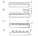
実施の形態4は、架橋性物質に光反射防止膜機能をもつ材料を用いる以外は、実施の形態1と同様である。図2は架橋性物質に光反射防止膜機能をもつ材料を用いた時の露光の状態を説明する概念図である。
【0050】
図2において、基盤11とフォトレジスト13の間の架橋性物質21は反射防止の機能を有する膜である。基盤1は、ニッケルなどの高反射率の材料であるので、実施の形態1におけるレーザ記録の際、反射光は定在波を生じる。レーザ波長をλ、架橋性物質21およびフォトレジスト13の屈折率と膜厚をそれぞれnc,dcおよびnr,drとし、その関係を数2の式で示す。
【0051】
【数2】
![]()
この数2の式が成り立つの時、レーザの定在波の節がフォトレジスト13の中に存在することになる。その場合、現像後のフォトレジスト13の突起の形状は節の影響を受けていびつな形状になる。
【0053】
この様な場合、架橋性物質21に光反射防止膜の特性を持つものを用いれば、露光時の、基盤11表面で反射するレーザの強い反射光を減じるので、フォトレジスト膜中に定在波の発生を無くすことができ、突起の歪みを無くすことができる。従って、現像後に顕在化するフォトレジスト突起の形状が定在波の節に影響されず、レーザのガウシャン型プロフィールとレジスト感度によって決まる形状を持ち、良質な突起形状を形成することができる。ここでは架橋性物質として有機ポリマー系の光反射防止膜を用いた。
【0054】
(実施の形態5)
実施の形態5は、架橋性物質と接触する基盤表面が凹凸形状である以外は、実施の形態1と同様である。図3は基盤表面が凹凸形状であるスタンパーの断面を示す概念図である。図3において基盤31の表面は微細な凹凸を有している。そのため架橋性物質層12と基盤31の接触面積が増え、両者の接着強度を増すことができる。従って、成形時の熱サイクルに対して基盤31と架橋性物質12の熱膨張係数の違いによって生じるせん断歪みに耐えることができる。
【0055】
基盤31の表面に微細な凹凸を与える方法としては、基盤31を不活性ガスのプラズマ
中に曝し、不活性ガスのイオン照射により微細な凹凸を与える方法や、或いは化学処理により基盤31の表面に微細な凹凸を形成する方法などがある。凹凸の大きさの一例としては0.1以上10nm以下である。
【0056】
(実施の形態6)
図4は上記の工法で作られたダイレクトスタンパーからディスクを作る工程を模式的に示す図である。図4(A)はディスクの樹脂注入を示す図である。図4(A)において、ダイレクトスタンパー41は、上記実施例の工法で作られた、図1(J)、または図3に示すダイレクトスタンパーである。スタンパー41は成形機の固定金型42に取付けられている。43は移動金型で樹脂44が型の中に注入されてから金型42の方に加圧される。
【0057】
図4(B)はダイレクトスタンパーからディスクの剥離工程を示す図である。図4(B)において、ディスクの加圧成形後、移動金型43が開き、ダイレクトスタンパー41の突起46がピット(窪み)47として転写されてディスク状に成形されたレプリカディスク45がダイレクトスタンパー41から剥離される。
【0058】
図4(C)は完成したレプリカディスクの断面を示す模式図である。図4(C)において、詳細は省くがレプリカディスク45に記録膜またはアルミなどの反射膜48がスパッタリング法で付けられる。
【0059】
CDディスクはレプリカディスクの厚みが1.2mmで、上記反射膜に保護膜をつけて完成する。DVDディスクのレプリカディスクは厚みが0.6mmで、反射膜48が付けられたレプリカディスクに信号の記録されていないダミーディスク49が接着層50を介して貼り合されて完成する。このタイプのディスクは、DVD5と呼ばれる。DVDディスクはこの他にダミーディスクではなく両面に信号が記録されたものや、2層ディスクの信号を片面から読み出すタイプのディスクもある。
【0060】
上記のようなディスクの成形工程では、高温の樹脂44が型内に注入されてスタンパー41の温度が上昇し、圧縮成形後、レプリカディスク45がスタンパーから剥離された後、スタンパー41の表面温度は室温の雰囲気に曝される。
【0061】
図5で示した従来のスタンパーは、この温度サイクルによって、金属の基盤と架橋性物質であるフォトレジストの突起の膨張収縮差によってせん断応力が境界部に作用し、遂にはフォトレジスト突起の欠落を起こしていた。このフォトレジスト突起の欠落は約5000〜10000ショットの成形回数を超えると顕著になり、PIエラーは規格の280以上になっていた。
【0062】
本実施例のダイレクトスタンパーでは、フォトレジストの突起が直接基盤に固定されているのではなく、基盤に設けられた架橋性物質の上に一体に近い構造で固定されている。すなわち、架橋性物質層はアンカーコートの役割を演じる。そのため、成形時の突起の欠落が大幅に減少し、実験では10万ショット以上の成形においてもフォトレジスト突起の欠陥は発見されず、PIエラーの増加も確認されなかった。また、架橋性物質層の剥離もなかった。DVDの信号再生特性で最も重要な項目は、ジッターであるが、本発明によるダイレクトスタンパーによるDVDディスクのジッターは規格の8%以下に対して、6%台前半を達成した。また、その値は10万ショット前後でも不変であった。従来のダイレクトスタンパーでは1万枚が限度なため、1枚のスタンパーで多くのディスクを成形できなかったが、本発明のダイレクトスタンパーでは、10万枚以上のディスクを一度に生産することが可能であり、品質が一定で、ディスク1枚当たりの製造コストを低く抑えられる。
【0063】
【発明の効果】
本発明によるスタンパーは、ディスクの信号を表すフォトレジストの層に形成された突起が、架橋性物質の層の上に形成され、互いに架橋しあって結合しているので、成形時の熱サイクルや応力に対して剥がれにくい。また、架橋性物質の層が有機系ポリマーの場合、フォトレジストの熱膨張係数と非常に近い値であり、成形時の熱サイクルによる膨張、収縮によって生じるせん断歪が小さい。従って、成形時にフォトレジストの層に形成された突起が剥がれにくい。
【0064】
従って、本発明によるスタンパーは、従来の基盤に直接レジスト突起を形成するスタンパーに比べ、ディスク成形のショット数が大幅に向上する。これにより同一スタンパーで10万枚以上の成形が可能であり、品質、性能が一定のディスクを安価に生産することができる。
【図面の簡単な説明】
【図1】本発明の実施の形態1〜3のダイレクトスタンパーの製造方法を示す図
【図2】本発明の実施の形態4の光反射防止膜機能有する架橋性物質の露光の状態を示す図
【図3】本発明の実施の形態5の基盤表面が凹凸形状であるスタンパーの断面を示す概念図
【図4】本発明の実施の形態6のダイレクトスタンパーからディスクを作る工程の模式図
【図5】従来のダイレクトスタンパーの製造方法を示す図
【符号の説明】
11 基盤
12 架橋性物質
13 第2の架橋物質であるフォトレジスト
14 レーザビーム
18 突起(突起状の第2の架橋物質)
21 光反射防止の機能を有する架橋性物質
31 表面に凹凸を有する基盤[0001]
TECHNICAL FIELD OF THE INVENTION
The present invention is used for forming an optical disc and an optical disc.RusuTamper, manufacturing method thereof, and optical diskAnd blanksIt is about.
[0002]
[Prior art]
Conventionally, a stamper for manufacturing an optical disk has been manufactured in a process called mastering. This method uses a technique generally called photolithography, and starts by forming a pattern of unevenness of a photoresist corresponding to a signal on a glass disk. The positive photoresist layer on the glass disk is spirally exposed to a laser beam whose intensity has been modulated according to the signal to be recorded, and developed to form pits (pits) in the resist in a track shape. is there. Thereafter, a conductive film is formed on the surface, and a thick nickel film is formed thereon by electroforming. The thick film is about 0.3 mm, and it is peeled off from the original glass disk to form a stamper. Projections (bumps) on which the pits of the photoresist are transferred are spirally formed on the nickel disk. By subjecting this to injection molding, an optical disk having a pit row containing information can be obtained.
[0003]
The process of making this stamper involves more than 10 steps and is time consuming and costly to manufacture. In addition, since there are many processes, there are many defects due to dust and human error, and the yield has been reduced.
[0004]
In recent years, attempts have been made to manufacture a stamper with fewer steps without requiring such many steps. In Japanese Patent Publication No. 2765421, a crosslinkable inorganic or crosslinkable organic layer is provided on a substrate, and a laser beam whose intensity is modulated by a recording signal is irradiated and developed to form a projection corresponding to a signal pattern on the substrate. There is shown a method in which the substrate is directly used as a stamper after the projections are provided and the projections are strengthened by heating. A conventional example will be described with reference to FIG. In FIG. 5A, a
[0005]
Japanese Patent Application Laid-Open No. 7-326077 discloses a method in which protrusions of a photoresist (crosslinkable substance) are formed on a substrate, crosslinking is promoted by heating at a high temperature, and the resultant is directly used as a direct stamper. This patent differs from the method of Japanese Patent Publication No. 2765421 in that a photoresist is selectively exposed to generate an acid. Thereafter, by heating the whole, the acid becomes a catalyst to cause crosslinking only in the exposed portion. Next, when the whole is exposed, an acid is generated in the previously unexposed area, and since it is not cross-linked, it is dissolved in a developing solution, and the first exposed area remains as a projection.
[0006]
[Patent Document 1]
Patent Publication No. 2765421
[Patent Document 2]
JP-A-7-326077
[0007]
[Problems to be solved by the invention]
However, all of the conventional direct stampers are formed by directly forming projections of an organic or inorganic photoresist (crosslinkable substance) on a nickel substrate. For this reason, the hardness of the photoresist is increased by the high-temperature baking, but the adhesive force between the photoresist and the metal is not originally strong. In the case of a DVD, the width of the projection of the photoresist is 0.3 μm and the length is the shortest, which is 0.4 μm, and the bonding area is very small.
[0008]
This direct stamper is attached to a mold of a molding machine, and forms a cavity with a mirror mold. A high-temperature resin is injected therein at a high pressure. At that time, the high-pressure resin causes the photoresist protrusion to peel off.
[0009]
Generally, the temperature of the mold is set at about 100 ° C., but the injected resin is a high temperature of about 300 ° C. or more. The thermal expansion and shrinkage in which the temperature of the direct stamper surface rises due to the injection of the resin and returns to the original temperature when the molded disk (optical disk) is removed is repeated. There is a large difference in the coefficient of thermal expansion between a metal such as nickel and the photoresist, and the stress due to the difference in thermal expansion repeatedly acts on the photoresist projections, and eventually peels off the substrate.
[0010]
When a disk such as a DVD (optical disk) is formed by a conventional direct stamper, a reproduction signal error of the DVD due to lack of a photoresist protrusion reaches an allowable limit value in about 5,000 to 10,000 shots. In DVD, an error due to a defect is called a PI error, and is determined to be 280 or less in 8 ECC blocks before error correction. Therefore, in the molding of a disc such as a DVD (optical disc) using a conventional direct stamper, it was not possible to mold about 5,000 to 10,000 shots or more.
[0011]
[Means for Solving the Problems]
To solve the above problems,Of the present inventionFirstThe manufacturing method of the stamperOn the foundationForming a layer of a crosslinkable substance on theLayer ofAfter the first cross-linking reaction, the cross-linkable substanceLayer ofForming a layer of photoresist on top of the photoresist,Layer ofExposure and development of the laser beam modulated by the signal to be recorded inAfter going, beforeCrosslinkable substance and said photoresistUpdate each layerIs subjected to a second cross-linking reaction to obtain the cross-linkable substanceLayer ofAnd the photoresistAnd layersIt is characterized by a bridge connection.
[0012]
Also,A second method for manufacturing a stamper according to the present invention includes:Crosslinkable materialOn the quality layerPhotoresistLayers are shapedLaser beam modulated by the signal to be recorded by rotating the formed baseThe desiredExpose the photoresist layer by focusing on spots,thisA latent image is spirally recorded on the photoresist layer, and thereafter, the photoresist layer is formed.ToDeveloping the photoresist layer, removing the portions other than the exposed portions, and removing the photoresist.Layer ofProtrusionThe shapeTo makeIt is characterized by.
[0013]
Also,In the first and second stamper manufacturing methods of the present invention,The photoresist is preferably a negative resist.
[0014]
Preferably, the material of the base is nickel.
[0015]
Further, it is preferable that the surface of the substrate in contact with the crosslinkable substance is subjected to an unevenness treatment of 1 nm or more and 10 nm or less.
[0016]
Next, the present inventionBuRanks isOn the foundationCrosslinkable substance layerWherein the layer of the crosslinkable substance is a layer in which the surface is incompletely crosslinked and further comprises a layer of the crosslinkable substance.uponToIt is characterized in that a photoresist layer is provided.
[0017]
Preferably, the photoresist is a negative resist.
[0018]
Preferably, the material of the base is nickel.
[0019]
In addition, it is preferable that the surface of the substrate in contact with the crosslinkable substance be subjected to an unevenness treatment of 1 nm or more and 10 nm or less.
[0020]
Next, the present inventionNoThe tamper isOn the foundationA layer of a crosslinkable substance is formed on the crosslinkable substance.Layer ofFirst crosslinking reactionAfter making the surface of the layer of the crosslinkable substance into an incomplete crosslinked state by applyingCrosslinkable substanceLayer ofA layer of photoresist on top of said photoresistLayer ofExposure and development of the laser beam modulated by the signal to be recorded inTo form protrusions in the photoresist layer.And then the crosslinkable substanceLayersThe photoresistLayer ofFurther, a second crosslinking reaction is performed, and the crosslinking substanceLayer ofAnd the photoresistLayers completelyCross-linkingOctopusAnd features.
[0021]
At this time, the laser beam modulated by the signal to be recordedThe desiredFocus on spotsTeExposing the photoresist layer,thisA latent image is recorded spirally on the photoresist layer, and then the photoresist layer is recorded.ToAnd then developing the photoresist layer to remove portions other than the exposed portions.so, The photoresistProtrusions are formed on the layer ofIt is suitable.
[0022]
Also, the second crosslinking reactionIsCrosslinkable substanceLayer ofWhenPhotoresist layerExposure to plasmaReaction, The crosslinkable substanceLayer ofWhenProtrusions formedThe Photo RegisAndCross-linking reaction takes place between the cross-linkable substancesLayer ofAnd the photoresistIn each of the layersPreferably, the crosslinking reaction is accelerated.
[0023]
Further, the second crosslinking reaction is a crosslinking substance.Layer ofWhenIn the photoresist layer where protrusions are formedUV irradiation and bakingProcessingBy the ultraviolet irradiation and the baking treatment, the crosslinkable substanceLayer ofWhenProtrusions formedThe photoresistLayer ofCross-linking reaction is carried out betweenLayer ofAnd the photoresistLayer ofIt is preferable that each of them promotes a crosslinking reaction.
[0024]
Finally, the optical disc of the present inventionManufactured by any of the above stampersIt is characterized by the following.
[0025]
Thereby, the binding between the projecting photoresist and the crosslinkable substance can be strengthened. Therefore, when molding an optical disc such as a DVD (optical disc) using a direct stamper having a protruding photoresist, a DVD reproduction signal error due to a lack of the protruding photoresist of the direct stamper can reduce a DVD reproduction error of 10,000 shots or more. Even molding can be prevented.
[0026]
BEST MODE FOR CARRYING OUT THE INVENTION
1 to 4 show an embodiment of the present invention.
[0027]
(Embodiment 1)
FIG. 1 shows an embodiment of a method for manufacturing a direct stamper according to the present invention.
[0028]
FIG. 1A is a diagram showing a state after a
[0029]
First, the
[0030]
In addition, some materials of the
[0031]
In any case, the first cross-linking reaction of the
Generally, an organic polymer becomes insoluble in a solvent when a few percent of crosslinking proceeds.
[0032]
FIG. 1E shows a state in which a
[0033]
Next, the
[0034]
FIG. 1G is a diagram showing a baking process after exposure. The acid generated in the exposed portions of the
[0035]
FIG. 1H is a view showing a state in which the portions other than the cross-linked portions of the
[0036]
FIG. 1 (I) is a step of further promoting the crosslinking of the photoresist of the
[0037]
One specific method for accelerating the crosslinking reaction (second crosslinking reaction) is to expose the entire substrate after development to plasma. As the plasma in this method, plasma using fluorine gas was used, and the entire substrate after development was exposed to the plasma, so that the effect was high. When a cross-linkable substance (photoresist) is exposed to the plasma, the projections of the photoresist are shaved and changed in shape by ions and radicals in the plasma. Therefore, the plasma exposure time is set to about several seconds. The cross-linkable substance and the protrusions of the photoresist that have been subjected to the plasma treatment for several seconds are hardened to the inside, and the hardness rate of the cross-linkable substance after the plasma treatment with the fluorine gas is 180 times greater than that after the oxygen ashing. Hardened near. The resist
[0038]
FIG. 1 (J) shows that after the second crosslinking, the
It is a figure which shows that it has become the structure 19 integrated by coupling. The base 11 on which the integrated structure 19 is formed on the front surface is processed into an inner and outer diameter so as to fit a mold of a molding machine, and the back surface is cut as required, whereby a direct stamper is completed. Note that these processes may be performed before the crosslinkable substance is applied to the base, that is, before FIG. 1A.
[0039]
Here, assuming that the temperature at the interface between the direct stamper and the molten resin injected into the surface thereof is T, T is obtained by the following equation (1).
[0040]
(Equation 1)
(Where ρ is specific gravity, C is specific heat, k is thermal conductivity, p is molten resin, m is direct stamper, respectively, Tpo is the temperature of the molten resin, and Tmo is the initial temperature of the direct stamper. .)
Although it depends on the molding conditions, in the case of a conventional DVD-ROM disc using a nickel direct stamper, the temperature of the mold of the molding machine to which the stamper is attached is set to 100 ° C., and the temperature of the molten resin is set to 360 ° C. Have been. When the molten resin comes into contact with the surface of the stamper, the temperature T at the interface of the molten resin is almost equal to the initial temperature of the stamper and becomes 110 ° C. or less because the thermal conductivity of nickel is much higher than that of the resin. Therefore, the molten resin starts to cool and solidify from the moment it contacts the stamper surface.
[0042]
In the case where the cross-linkable substance made of an organic polymer and the photoresist form the surface of the direct stamper made of nickel as in this embodiment, the temperature of the interface of the molten resin is higher than in the above case. When there is no difference in specific gravity, specific heat and thermal conductivity between the crosslinkable substance and the material of the photoresist and the surface of the direct stamper, the temperature T at the interface of the molten resin is about 230 ° C. at the above temperature setting. In this embodiment, since the heat sink has nickel under the crosslinkable substance, the temperature is expected to drop to 230 ° C. or less. However, in any case, the direct stamper according to the present embodiment is deteriorated by heat during molding because the heat-resistant temperature of the protrusion of the second crosslinkable substance is 250 ° C. or higher due to crosslinking as described above. I can't.
[0043]
(Embodiment 2)
The second embodiment is different from the first embodiment except for the method (second cross-linking reaction) shown in FIG. The same is true. In this method, the
[0044]
Here, when the photoresist is a chemically amplified resist, baking after irradiation with ultraviolet rays promotes the second crosslinking reaction.
[0045]
When the photoresist is a novolac resin other than the chemically amplified type, irradiation with far ultraviolet rays in a state where the moisture in the resist has been eliminated by baking effectively promotes the second crosslinking reaction.
[0046]
In the second embodiment of the present invention, a chemically amplified photoresist is used, and the substrate after development is irradiated with far ultraviolet rays having a wavelength of 254 nm, and then baked at 150 to 250 ° C. for 10 to 20 minutes. Was performed.
[0047]
In this case, as in the first embodiment, the cross-linking of the cross-linkable substance and the protrusions of the photoresist and the respective cross-links proceeded, and the heat resistance temperature of the entire substrate was 250 ° C. or higher. Also in this case, the resist
[0048]
(Embodiment 3)
The third embodiment is the same as the first embodiment except that the same substance as the photoresist is used as the crosslinkable substance. When the same material as the photoresist is used as the crosslinkable substance, crosslinking between the two becomes easier to occur, and the adhesive strength between the two further increases. Further, since the thermal expansion coefficient is the same, no shear strain is generated at the boundary surface even when repeatedly subjected to a thermal change during molding, and the resistance due to the thermal change is further enhanced. In this example, a polymer based on a novolak type phenol resin was used in both cases.
[0049]
(Embodiment 4)
The fourth embodiment is the same as the first embodiment, except that a material having a light reflection preventing film function is used for the crosslinkable substance. FIG. 2 is a conceptual diagram illustrating an exposure state when a material having a light reflection preventing film function is used as a crosslinkable substance.
[0050]
In FIG. 2, the
[0051]
(Equation 2)
![]()
When the
[0053]
In such a case, if the
[0054]
(Embodiment 5)
The fifth embodiment is the same as the first embodiment, except that the surface of the base in contact with the crosslinkable substance has an uneven shape. FIG. 3 is a conceptual diagram showing a cross section of a stamper in which the substrate surface has an uneven shape. In FIG. 3, the surface of the
[0055]
As a method for providing fine irregularities on the surface of the
There is a method in which fine irregularities are given by irradiating the inside of the
[0056]
(Embodiment 6)
FIG. 4 is a diagram schematically showing a process of making a disc from the direct stamper made by the above-described method. FIG. 4A is a diagram showing resin injection of a disk. In FIG. 4A, a
[0057]
FIG. 4B is a diagram showing a step of separating the disk from the direct stamper. In FIG. 4B, after pressing the disk, the
[0058]
FIG. 4C is a schematic view showing a cross section of the completed replica disk. In FIG. 4C, a recording film or a
[0059]
The CD disk has a replica disk thickness of 1.2 mm and is completed by providing a protective film on the reflective film. The replica disk of the DVD disk has a thickness of 0.6 mm and is completed by bonding a
[0060]
In the above-described disk molding process, the high-
[0061]
In the conventional stamper shown in FIG. 5, due to this temperature cycle, the shear stress acts on the boundary due to the difference in expansion and contraction of the protrusions of the metal substrate and the photoresist, which is a crosslinkable substance, and eventually the lack of the photoresist protrusions occurs. Was awake. The lack of the photoresist protrusion became remarkable when the number of moldings exceeded about 5,000 to 10,000 shots, and the PI error was 280 or more of the standard.
[0062]
In the direct stamper of this embodiment, the protrusions of the photoresist are not directly fixed to the base but are fixed on a cross-linkable substance provided on the base in a structure almost integral with the base. That is, the crosslinkable material layer plays the role of an anchor coat. For this reason, the lack of protrusions during molding was significantly reduced, and no defects in the photoresist protrusions were found even in molding of 100,000 shots or more, and no increase in PI error was confirmed in experiments. In addition, there was no peeling of the crosslinkable substance layer. The most important item in the DVD signal reproduction characteristics is the jitter. The jitter of the DVD disk by the direct stamper according to the present invention has achieved the lower 6% level compared with 8% or less of the standard. The value was not changed even after about 100,000 shots. Since the conventional direct stamper has a limit of 10,000, it was not possible to mold many discs with one stamper. However, the direct stamper of the present invention can produce 100,000 or more discs at a time. Yes, the quality is constant, and the manufacturing cost per disc can be kept low.
[0063]
【The invention's effect】
According to the inventionRusuTamper is a photoresist that represents the signal on the discFormed in the layer ofThe protrusion is a cross-linkable substanceLayer ofAre formed on top of each other and are cross-linked to each other, so that they are not easily peeled off due to a thermal cycle or stress during molding. Also, a crosslinkable substanceLayer ofIs an organic polymer, the value is very close to the thermal expansion coefficient of the photoresist, and the shear strain caused by expansion and contraction due to the thermal cycle during molding is small. Therefore, during moldingFormed in a layer of photoresistThe protrusions are difficult to peel off.
[0064]
Therefore, according to the present invention,RusuThe tamper greatly increases the number of shots for disk forming as compared to a conventional stamper in which resist projections are formed directly on a substrate. As a result, 100,000 or more sheets can be molded with the same stamper, and disks with constant quality and performance can be produced at low cost.
[Brief description of the drawings]
FIG. 1 is a diagram showing a method for manufacturing a direct stamper according to first to third embodiments of the present invention.
FIG. 2 is a diagram showing an exposure state of a crosslinkable substance having a light reflection preventing film function according to a fourth embodiment of the present invention.
FIG. 3 is a conceptual diagram showing a cross section of a stamper according to a fifth embodiment of the present invention in which the base surface has an uneven shape.
FIG. 4 is a schematic view of a process of making a disc from a direct stamper according to a sixth embodiment of the present invention.
FIG. 5 is a diagram showing a conventional direct stamper manufacturing method.
[Explanation of symbols]
11 Base
12 Crosslinkable substances
13. Photoresist as the second cross-linking substance
14 Laser beam
18. Projection (projection-like second cross-linking substance)
21 Crosslinkable substance having antireflection function
31 Substrate with uneven surface
Claims (5)
を特徴とするスタンパーの製造方法。 After forming a negative type photoresist layer on a substrate, performing a baking process on the photoresist layer, and then irradiating ultraviolet rays to make the surface incompletely crosslinked, the photoresist layer A photoresist layer of the same material as that of the photoresist is further formed on the photoresist layer, and thereafter, exposure and development of a laser beam modulated by a signal to be recorded on the photoresist layer are performed. A method of manufacturing a stamper , wherein each of the photoresist layers is further baked to completely cross-link the two photoresist layers .
を特徴とするブランクスの製造方法。 Having a negative photoresist layer on the substrate, performing a baking treatment on the negative photoresist layer, and then irradiating ultraviolet light to make the surface incompletely crosslinked, further comprising the photoresist A blanks manufacturing method, comprising: providing a photoresist layer of the same substance as described above .
Priority Applications (1)
| Application Number | Priority Date | Filing Date | Title |
|---|---|---|---|
| JP2002306937A JP3596543B2 (en) | 2001-10-23 | 2002-10-22 | Stamper, method of manufacturing the same, optical disk and blanks |
Applications Claiming Priority (3)
| Application Number | Priority Date | Filing Date | Title |
|---|---|---|---|
| JP2001324707 | 2001-10-23 | ||
| JP2001-324707 | 2001-10-23 | ||
| JP2002306937A JP3596543B2 (en) | 2001-10-23 | 2002-10-22 | Stamper, method of manufacturing the same, optical disk and blanks |
Publications (3)
| Publication Number | Publication Date |
|---|---|
| JP2003203396A JP2003203396A (en) | 2003-07-18 |
| JP2003203396A5 JP2003203396A5 (en) | 2004-11-11 |
| JP3596543B2 true JP3596543B2 (en) | 2004-12-02 |
Family
ID=27666381
Family Applications (1)
| Application Number | Title | Priority Date | Filing Date |
|---|---|---|---|
| JP2002306937A Expired - Fee Related JP3596543B2 (en) | 2001-10-23 | 2002-10-22 | Stamper, method of manufacturing the same, optical disk and blanks |
Country Status (1)
| Country | Link |
|---|---|
| JP (1) | JP3596543B2 (en) |
Families Citing this family (2)
| Publication number | Priority date | Publication date | Assignee | Title |
|---|---|---|---|---|
| CN102023476B (en) * | 2009-09-15 | 2013-06-12 | 中芯国际集成电路制造(上海)有限公司 | Semiconductor photoetching process method for forming micro-sized structure |
| WO2011125099A1 (en) * | 2010-04-02 | 2011-10-13 | 株式会社 東芝 | Master for producing stamper |
-
2002
- 2002-10-22 JP JP2002306937A patent/JP3596543B2/en not_active Expired - Fee Related
Also Published As
| Publication number | Publication date |
|---|---|
| JP2003203396A (en) | 2003-07-18 |
Similar Documents
| Publication | Publication Date | Title |
|---|---|---|
| US5480763A (en) | Method for manufacturing a stamper for high-density recording discs | |
| US6927016B2 (en) | Blank disc and direct stamper and its manufacturing method | |
| JP3596543B2 (en) | Stamper, method of manufacturing the same, optical disk and blanks | |
| JP2006338844A (en) | Stamper for preparing optical disk and method for manufacturing the same | |
| JPH11296918A (en) | Manufacture of stamper for optical information recording medium | |
| JP4366193B2 (en) | Stamper master manufacturing method and stamper manufacturing method | |
| JP2003203396A5 (en) | ||
| JPWO2003088235A6 (en) | Stamper master and manufacturing method thereof, stamper and manufacturing method thereof, and optical disc | |
| JP2001338444A (en) | Method for manufacturing original disk, stamper and information recording medium | |
| US7067238B2 (en) | Method for manufacturing a substrate for use in a stamper manufacturing process, as well as a substrate obtained by using such a method | |
| JP2004152397A (en) | Base for forming optical disk, manufacturing method therefor, and blanks of base for forming optical disk | |
| JPH11102541A (en) | Production method of matrix of optical disk | |
| JP2003123329A (en) | Stamper and production method therefor | |
| JP2002245685A (en) | Method of forming fine pattern | |
| JP2004062982A (en) | Manufacturing method of blank base for stamper | |
| JP2765421B2 (en) | Optical disk stamper and method of manufacturing the same | |
| JP2767638B2 (en) | Manufacturing method of stamper for optical disk | |
| JPH11110831A (en) | Production of master disk for manufacturing optical disk | |
| JP2003217178A (en) | Optical disk and method for manufacturing its master disk | |
| JP2004362752A (en) | Method for manufacturing master disk for optical disk | |
| JP2005032281A (en) | Manufacturing method of optical original disk, optical original disk, manufacturing method of stamper, and stamper and optical disk | |
| JPH11353719A (en) | Production of optical disk master | |
| JP2002092981A (en) | Method for producing stamper and method for producing optical recording medium | |
| JP2003242695A (en) | Method of manufacturing master disk for optical disk, method of manufacturing stamper for optical disk, stamper for optical disk, and method of manufacturing molded resin for optical disk, and molded substrate for optical disk | |
| JP3555249B2 (en) | Blank master for optical disk, method of manufacturing stamper for optical disk, method of manufacturing optical disk |
Legal Events
| Date | Code | Title | Description |
|---|---|---|---|
| A975 | Report on accelerated examination |
Free format text: JAPANESE INTERMEDIATE CODE: A971005 Effective date: 20040121 |
|
| A131 | Notification of reasons for refusal |
Free format text: JAPANESE INTERMEDIATE CODE: A131 Effective date: 20040518 |
|
| A521 | Written amendment |
Free format text: JAPANESE INTERMEDIATE CODE: A523 Effective date: 20040720 |
|
| TRDD | Decision of grant or rejection written | ||
| A01 | Written decision to grant a patent or to grant a registration (utility model) |
Free format text: JAPANESE INTERMEDIATE CODE: A01 Effective date: 20040817 |
|
| A61 | First payment of annual fees (during grant procedure) |
Free format text: JAPANESE INTERMEDIATE CODE: A61 Effective date: 20040830 |
|
| FPAY | Renewal fee payment (event date is renewal date of database) |
Free format text: PAYMENT UNTIL: 20080917 Year of fee payment: 4 |
|
| FPAY | Renewal fee payment (event date is renewal date of database) |
Free format text: PAYMENT UNTIL: 20080917 Year of fee payment: 4 |
|
| FPAY | Renewal fee payment (event date is renewal date of database) |
Free format text: PAYMENT UNTIL: 20090917 Year of fee payment: 5 |
|
| FPAY | Renewal fee payment (event date is renewal date of database) |
Free format text: PAYMENT UNTIL: 20090917 Year of fee payment: 5 |
|
| FPAY | Renewal fee payment (event date is renewal date of database) |
Free format text: PAYMENT UNTIL: 20100917 Year of fee payment: 6 |
|
| FPAY | Renewal fee payment (event date is renewal date of database) |
Free format text: PAYMENT UNTIL: 20110917 Year of fee payment: 7 |
|
| LAPS | Cancellation because of no payment of annual fees |