JP3595273B2 - Panel display device - Google Patents
Panel display device Download PDFInfo
- Publication number
- JP3595273B2 JP3595273B2 JP2001068720A JP2001068720A JP3595273B2 JP 3595273 B2 JP3595273 B2 JP 3595273B2 JP 2001068720 A JP2001068720 A JP 2001068720A JP 2001068720 A JP2001068720 A JP 2001068720A JP 3595273 B2 JP3595273 B2 JP 3595273B2
- Authority
- JP
- Japan
- Prior art keywords
- pulse
- sustain
- voltage
- discharge
- sustain pulse
- Prior art date
- Legal status (The legal status is an assumption and is not a legal conclusion. Google has not performed a legal analysis and makes no representation as to the accuracy of the status listed.)
- Expired - Fee Related
Links
Images


Description
【0001】
【発明の属する技術分野】
本発明は、コンピュータおよびテレビ等の画像表示に用いるガス放電パネル表示装置及びガス放電パネルの駆動方法に関し、特に、誘電体層に電荷をためることによって画像を書き込み、放電維持することによって発光させるAC型PDPに関する。
【0002】
【従来の技術】
近年、コンピュータやテレビ等に用いられているディスプレイ装置において、プラズマディスプレイパネル(Plasma Display Panel,以下PDPと記載する)をはじめとするガス放電パネルは、大型で薄型軽量を実現することのできるものとして注目されている。
【0003】
このPDPは、マトリックス状に配列された放電セルが選択的に発光することによって画像表示される。
PDPは、大別して直流型(DC型)と交流型(AC型)とに分けられるが、現在では大型化に適したAC型が主流となっている。
AC型PDPにおいて、各放電セルは元来、点灯もしくは消灯の2階調しか表現できないので、1フレーム(1フィールド)を複数のサブフレーム(サブフィールド)に分割し、各サブフレームにおける点灯/消灯を組み合わせて中間階調を表現するフレーム内時分割階調表示方式が用いられている。
【0004】
そして、各サブフレームでは、ADS(Address Display−period Separation)方式によって画像表示する。即ち、各サブフレームは、図25に示されように、初期化期間、書込期間、放電維持期間、消去期間という一連のシーケンスで構成されており、書込期間には、点灯すべき放電セルに壁電荷を蓄積して画像を書き込み、放電維持期間においては、全体の放電セルに一括して、交流の維持パルスを印加する。このとき印加する維持パルスの電圧は、壁電荷が蓄積された放電セルでは放電しそれ以外のセルでは放電しないような範囲(通常150〜200Vの範囲)内に設定される。
【0005】
この発光原理は基本的に蛍光灯と同様であって、維持パルスを印加して通常のグロー放電を発生させることによりXeから紫外線(Xe共鳴線、波長147nm)を発生し、蛍光体を励起発光させるが、放電エネルギの紫外線への変換効率や、蛍光体における可視光への変換効率が悪いので、蛍光灯のように高い輝度を得ることは難しい。
【0006】
また、他のディスプレイと同様、PDPにおいても高精細化に対する要求がある(例えば、近年実用化されつつあるハイビジョンテレビでは、フルスペックで画素数が1920×1080と高精細である。)が、このような高精細のPDPにおいては、発光効率は更に低くなりやすい。
【0007】
【発明が解決しようとする課題】
このような背景のもとで、PDPにおいて発光効率(投入する電力量に対する発光量)を向上させることが望まれる。この課題に対して、例えば、PDPの構造を改良することによって発光効率を向上させる技術や、紫外線の発光に寄与しない電流(無効電流)を回収する技術も開発されているが、無効電流の発生を低減する技術も望まれている。
【0008】
また、図25に示されように、維持パルスとしては、一般的に矩形波が用いられている。この矩形波は三角関数波のような波形と比べて立ち上がりがシャープであるため、基本的には、維持パルスに矩形波を用いれば、立ち上がり開始から比較的短時間で放電を開始させることができるので、比較的安定した画像を表示することができる。
【0009】
しかしながら、維持パルスを印加するときに、その立ち上がりからかなり遅れて放電が開始されるといういわゆる「放電遅れ」が、ある程度の確率で発生する。特に放電維持期間において印加される先頭の維持パルスにおいては放電遅れが発生しやすい。
このような「放電遅れ」は、表示される画像の画質を低下させる要因である。即ち、PDPには数多くの放電セルが配列されているが、上記のように「放電遅れ」がある程度の確率で発生すると、その中の点灯すべき放電セルの一部で「放電遅れ」が生じて点灯不良が発生し、表示される画像の画質が低下してしまうので、これを改善する技術も望まれる。
【0010】
本発明は、このような課題に鑑み、PDPをはじめとするガス放電パネルを駆動する際に、無効電流の発生を抑えて発光効率を向上させることを第1の目的とする。
また、放電維持期間における放電遅れの発生を抑えて画質を向上させることを第2の目的とする。
【0011】
【課題を解決するための手段】
上記第1の目的を達成するため、本発明は、維持パルスを印加する際に、その立ち上がりに要する時間に対して3倍の時間がピーク時点から経過するまでに立ち下がりが終了するような電流波形が形成されるよう、維持パルスの波形を規定することとした。
【0012】
また、上記特徴を持つ電流波形を形成するために、維持パルスを印加する際に、当該維持パルスに次の第1〜第3のいずれかの特徴を加えることとた。
第1の特徴は、維持パルスの先縁(パルス立ち上がり)に先立って、当該維持パルスと逆極性のパルスを短時間印加することである。
第2の特徴は、維持パルスの先縁(パルスの立ち上がり)から一定期間において、それ以降に印加される電圧より絶対値において高電圧が印加されるような波形に設定することである。
【0013】
第3の特徴は、維持パルスの後縁(パルス立ち下がり)直後において、これと逆極性のパルスを印加することである。
上記特徴を持つ電流波形が形成されると、一般的な波形の維持パルスを印加する場合と比べて、無効電流が抑制されるので、発光効率を向上させることができる。
【0014】
また、上記第1〜第3の特徴を維持パルスに加えると、上述した発光効率向上に加えて、各々次のような効果を奏する。
第1の特徴を維持パルスに加えると、初期に逆極性パルスを印加する際に、一方の電極から他方の電極に向かって電子が動くが、それが他方の電極に到達する前に、維持パルスの印加が始まることによって一方の電極側に引き戻される。
【0015】
このように初期に放電空間内を電子が往復運動することによって、発光に寄与する荷電粒子(電子やイオン)が多く生成されるので、更に発光効率が向上される。
また、電極間を荷電粒子が往復することにより、放電の種火が形成され、この種火によって確率よく放電開始(EVOLUTION OF DISCHARGE)されるため、第2の目的である放電遅れの抑制もなされる。
【0016】
なお、上記効果を確実に得るために、逆極性パルスの電圧は、維持パルス電圧に対して、電圧絶対値を1.0倍以上に設定することが好ましく、更に、維持パルス電圧に対して電圧絶対値を1.5倍以上に設定することが好ましい。
また、逆極性パルスを印加する期間については、この時間を100ns以下に設定することが好ましい。
【0017】
特に、維持パルス電圧に対して電圧絶対値が1.0倍以上になる時間は、100ns以下に設定することが好ましく、更に50ns以下とすることが望ましい。
第2の特徴を維持パルスに加えるた場合も、各維持パルスの立ち上がりから一定期間において高い電圧が印加されるので、確実に放電が開始され、放電遅れが抑えられる。
【0018】
特に、この一定期間において、放電セルの放電開始電圧以上の高電圧を印加すればその効果は顕著である。
ここで、維持パルス先縁から一定期間において、それ以降に印加される維持電圧より絶対値において50V以上高い電圧が印加されるようにするのが好ましい。
【0019】
また、一般的に高電圧を印加すると誘電体層の絶縁破壊や消費電力の増大を引き起こしやすいが、高電圧(放電セルの放電開始電圧以上の電圧)を印加する時間を100ns以下もしくは10ns以下といった短期間に設定すれば、誘電体層の絶縁破壊や消費電力の増大を回避することができる。
第3の特徴を維持パルスに加えると、維持パルス立ち下がり後において放電セル内に残っているイオンに起因する無効電流が抑えられる。
【0020】
即ち、パルス立ち下がり後において放電セル内に残っているイオンは低活性であって発光には寄与しないため、これが電極に到達すると無効電流が発生して発光効率が低下する要因となるが、維持パルスに第3の特徴を加えれば、当該無効電流が抑えられるので、この点で発光効率の向上に寄与するところが大きい。
ここで、この逆極性パルスについても、電圧絶対値の最高値を50V以上とすることが好ましい。
【0021】
また、この逆極性パルスを印加する時間は、100ns以下とすること、更に10ns以下とすることが好ましい。
ところで、1つの放電維持期間においては、通常、各放電セルに対して連続的に複数の維持パルスが極性を切り替えながら印加される。そこで、十分な効果を奏するために、その連続する維持パルスすべてに対して上記のような波形の特徴を適用することが好ましいが、一部の維持パルスに対してだけ上記波形の特徴を適用してもよい。但し、その場合も、少なくとも放電維持期間における先頭の維持パルスに対しては、上記波形の特徴を適用すべきである。
【0022】
【発明の実施の形態】
(表示装置について全体的な説明)
先ず、本実施形態にかかるPDP表示装置について、全体的な構成を説明する。
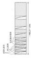
このPDP表示装置は、交流面放電型(AC型)PDPとその駆動装置から構成される。図1は、このPDPの見取図である。
【0023】
このPDPにおいては、前面基板11と背面基板12とが、互いに平行に間隙をおいて対峙して配置され、外周部が封止されている。
前面基板11の対向面上には、ストライプ状の走査電極群19a及び維持電極群19bが互いに平行に形成され、当該電極群19a、19bは、鉛ガラスなどからなる誘電体層17で覆われて、誘電体層17の表面は、MgO膜からなる保護層18で覆われている。背面基板12の対向面上には、ストライプ状のデータ電極群14とその表面を覆う鉛ガラスなどからなる誘電体層13が設けられ、その上に、データ電極群14と平行に隔壁15が配設されている。前面基板11と背面基板12との間隙は、隔壁15によって100〜200μm程度の間隔で仕切られ、放電ガスが封入されている。放電ガスの封入圧力は、パネル内部が外部の圧力(大気圧)に対して負圧となるよう、通常は1×10⁴〜7×10⁴Pa程度の範囲に設定されるが、8×10⁴Pa以上の高い圧力に設定する方が高発光効率を得るのに有利である。
【0024】
図2は、このPDPの電極マトリックスを示す図である。電極群19a、19bと、データ電極群14とは、互いに直交して配設されており、前面基板11及び背面基板12間の空間において、電極が交差するところに放電セルが形成されている。隣り合う放電セルの間は隔壁15で仕切られて、隣接する放電セルへの放電拡散が遮断されるようになっているため、解像度の高い表示を行うことができる。
【0025】
単色表示用のPDPでは、放電ガスとして、ネオンを中心とした混合ガスが用いられ、放電の際に可視域で発光することにより表示するが、図1のようなカラー表示用のPDPでは、放電セルの内壁に、三原色である赤(R)、緑(G)、青(B)の蛍光体からなる蛍光体層16を形成しておき、放電ガスとしてキセノンを中心とした混合ガス(ネオン−キセノンやヘリウム−キセノン)が用いられ、放電に伴って発生する紫外線を蛍光体層16で各色の可視光に変換することによりカラー表示を行う。
【0026】
このPDPは、フレーム内時分割階調表示方式を用いて駆動される。
図3は、256階調を表現する場合における1フレームの分割方法を示す図であって、横方向は時間、斜線部は放電維持期間を示している。
例えば、図3に示される分割方法の例では、1フレームは、8個のサブフレームで構成され、各サブフレームの放電維持期間の比は、1,2,4,8,16,32,64,128に設定されており、この8ビットバイナリの組み合わせによって256階調を表現できる。なお、NTSC方式のテレビ映像においては、1秒間あたり60枚のフレームで映像が構成されているため、1フレームの時間は16.7msに設定されている。
【0027】
各サブフレームでは、ADS方式によってPDPに画像を表示する。即ち、各サブフレームは、初期化期間、書込期間、放電維持期間、消去期間という一連のシーケンスで構成されている。
図4は、本実施形態において、1つのサブフレームにおいて各電極にパルスを印加するときのタイミングチャートである。
【0028】
初期化期間には、走査電極群19aの全体に一括して初期化パルスを印加することにより全ての放電セルの状態を初期化する。
書込期間には、走査電極群19aに走査パルスを順次印加しながらデータ電極群14の中の選択された電極にデータパルスを印加することにより、点灯させようとする放電セルに壁電荷を蓄積し、1画面分の画素情報を書き込む。
【0029】
放電維持期間には、走査電極群19aと維持電極群19b間に一括して、極性を入れ替えながら維持パルスを印加することによって、壁電荷が蓄積された放電セルで放電を起こして所定の時間発光させる。
図4に示すように、各維持パルスは、単純な矩形波ではなく、特有の波形となっているが、この点については後で詳述する。
【0030】
消去期間には、幅の狭い消去パルスを走査電極群19a又は維持電極群19bに一括して印加することによって放電セルの壁電荷を消去する。
(駆動装置及び駆動方法についての詳細な説明)
図5は、駆動装置100の構成を示すブロック図である。
この駆動装置100は、外部の映像出力器から入力されてくる映像データを処理するプリプロセッサ101、処理された映像データを格納するフレームメモリ102、フレーム毎及びサブフレーム毎に同期パルスを生成する同期パルス生成部103、走査電極群19aにパルスを印加するスキャンドライバ104、維持電極群19bにパルスを印加するサステインドライバ105、データ電極群14にパルスを印加するデータドライバ106から構成されている。
【0031】
プリプロセッサ101は、入力されてくる映像データからフレーム毎の映像データ(フレーム映像データ)を抽出し、抽出したフレーム映像データから各サブフレームの映像データ(サブフレーム映像データ)を作成してフレームメモリ102に格納する。また、フレームメモリ102に格納されているカレントサブフレーム映像データから1ラインづつデータドライバ106にデータを出力したり、入力される映像データから水平同期信号、垂直同期信号などの同期信号を検出し、同期パルス生成部103にフレームごと及びサブフレームごとに同期信号を送ることも行う。
【0032】
フレームメモリ102は、フレーム毎に、各サブフレーム映像データを分割して格納できるものである。
具体的には、フレームメモリ102は、1フレーム分のメモリ領域(8個のサブフレーム映像を記憶)を2個備える2ポートフレームメモリであって、一方のメモリ領域にフレーム映像データを書き込みながら、他方のメモリ領域から、これに書き込まれているフレーム映像データを読み出す動作を交互に行うことができるようになっている。
【0033】
同期パルス生成部103は、プリプロセッサ101からフレームごと及びサブフレームごとに送られて来る同期信号を参照して、初期化パルス,走査パルス,維持パルス,消去パルスを立ち上がらせるタイミングを指示するトリガ信号を生成して、各ドライバ104〜106に送る。
スキャンドライバ104は、同期パルス生成部103から送られてくるトリガ信号に呼応して、初期化パルス、走査パルス、維持パルス、消去パルスを生成して印加する。
【0034】
図6は、スキャンドライバ104の構成を示すブロック図である。
初期化パルス,維持パルス,消去パルスは、全ての走査電極19aに共通して印加されるものである。
そのため、図6に示すように、スキャンドライバ104には、各パルスを発生するために3つパルス発生器(初期化パルス発生器111、維持パルス発生器112a、消去パルス発生器113)が備えられている。そして、これら3つのパルス発生器は、フローティンググラウンド方式で直列に接続され、同期パルス生成部103からのトリガ信号に応じて作動することによって、初期化パルス,維持パルス,消去パルスが択一的に、走査電極群19aに印加されるようになっている。
【0035】
またスキャンドライバ104は、走査電極19a1,19a2…19aNに順に走査パルスを印加するために、ここでは図6に示すように、走査パルス発生器114と、これに接続されたマルチプレクサ115とを備え、同期パルス生成部103からのトリガ信号に応じて、走査パルス発生器114でパルスを発生すると共にマルチプレクサ115で切り換えて出力する方式をとっているが、各走査電極19a毎に個別に走査パルス発生回路を設けた構成とすることも可能である。
【0036】
そして、上記3つパルス発生器111〜113からの出力と、走査パルス発生器114からの出力とを、択一的に走査電極群19aに印加するためにスイッチSW1及びSW2が設けられている。
サステインドライバ105は、維持パルス発生器112bを備え、同期パルス生成部103からのトリガ信号に呼応して維持パルスを生成して維持電極群19bに印加する。
【0037】
データドライバ106は、シリアルに入力される1ラインに相当するサブフィールド情報に基づいて、データパルスをデータ電極群141〜14Mにパラレルに出力するものである。
図7は、データドライバ106の構成を示すブロック図である。
データドライバ106は、サブフレーム映像データを1走査ライン分づつ取り込む第1ラッチ回路121、これを記憶する第2ラッチ回路122、データパルスを発生するデータパルス発生器123、各データ電極141〜14Mの入口に設けられたANDゲート1241〜124Mから構成されている。
【0038】
第1ラッチ回路121では、プリプロセッサ101から順に送られてくるサブフレーム映像データをCLK信号に同期して数ビットづつ順に取り込み、1走査ライン分のサブフレーム映像データ(データ電極141〜14Mの各々についてデータパルスを印加するか否かを示す情報)がラッチされたら、それを第2ラッチ回路122にまとめて移動する。第2ラッチ回路122は、同期パルス生成部103から送られてくるトリガ信号に呼応して、ANDゲート1241〜124Mの中でデータパルスを印加するデータ電極に対応するものを開く。そして、データパルス発生器123では、これと同期してデータパルスを発生する。これによって、ANDゲートが開かれたものに対応するデータ電極にデータパルスが印加される。
【0039】
このような駆動装置100において、以下に示すように、初期化期間,書込期間,放電維持期間,消去期間という一連のシーケンスによって構成される1サブフレーム分の動作を8回繰返すことによって、1フレームの画像表示が行われる。なお、疑似輪郭対策のためサブフレームの数は8より多く設定することもある。
【0040】
初期化期間においては、スキャンドライバ104のスイッチSW1はON、SW2はOFFとし、初期化パルス発生器111で 全ての走査電極19aに一括して初期化パルスを印加することによって、全ての放電セルで初期化放電を行い、各放電セルに壁電荷を蓄積する。ここで、各放電セルにある程度の壁電圧をかけることによって、次の書込期間における書込放電の立ち上がりを早めることができる。
【0041】
書込期間においては、スキャンドライバ104のスイッチSW2はON、SW1はOFFとし、走査パルス発生器114で発生する負電圧の走査パルスを、第1行目の走査電極19a1〜最終行の走査電極19aNに対して順に印加する。そして、これにタイミングを合わせて、データドライバ106は、データ電極141〜14Mの中の点灯しようとする放電セルに対応するものに、正電圧のデータパルスを印加することによって書込放電を行い、その放電セルに壁電荷を蓄積する。このようにして、点灯しようとする放電セルの誘電体層の表面に壁電荷を蓄積することによって、1画面分の潜像が書き込まれることになる。
【0042】
走査パルス及びデータパルスのパルス幅(書込パルス幅)は、駆動を高速にするためにはできるだけ短く設定するのが望ましいが、書込パルス幅が短か過ぎると書き込み不良が生じやすくなる。また、回路上の制約からも、パルス幅は通常1.0μsec程度以上に設定する必要がある。
放電維持期間においては、スキャンドライバ104のスイッチSW1はON、SW2はOFFとし、維持パルス発生器112aで走査電極群19aに一括して一定の長さ(例えば1〜5μsec)の放電パルスを印加する動作と、サステインドライバ105の維持パルス発生器112bで維持電極群19bに一括して一定の長さの放電パルスを印加する動作を交互に繰り返す。
【0043】
これによって、書込期間に壁電荷が蓄積された放電セルにおいて、誘電体層表面の電位が放電開始電圧を上回ることによって放電が生じ、当該放電セル内では、この維持放電に伴って紫外線が発光され、これが蛍光体層で可視光に変換されることによって蛍光体層の色に対応する可視光の発光がなされる。
消去期間においては、スキャンドライバ104のスイッチSW1はON、SW2はOFFとし、消去パルス発生器113から幅の狭い消去パルスを走査電極群19aに一括して印加し、不完全な放電を発生することによって、各放電セルにおける壁電荷を消去する。
【0044】
〈放電維持期間におけるパルス波形について〉
放電維持期間において、走査電極群19aと維持電極群19bとの間に印加される維持パルスの波形の特徴やその効果などについて、まず概要を説明する。
本発明では、維持パルスを印加する際に、そのピークまでの立ち上がりに要する時間に対して3倍の時間がピーク時点から経過するまでに立ち下がりが終了するような特徴を備える電流波形が形成されるように、維持パルスの波形を調整した。
【0045】
即ち、維持パルスを印加する際に、立ち上がりに要する時間に対して3倍の時間がピーク時点から経過した時には、電流が極めて小さくなるように調整することによって無効電流を抑制し、発光効率を向上させることを図った。
また、上記特徴を持つ電流波形は、維持パルスを印加する際に、次の第1〜第3のいずれかの特徴を付加することによって得られることも把握した。
【0046】
第1の特徴:維持パルスの先縁(パルス立ち上がり)に先立って、当該維持パルスと逆極性パルスを短時間印加する。
第2の特徴:維持パルスの先縁(パルスの立ち上がり)から一定期間において、それ以降に印加される電圧より絶対値において高電圧が印加されるような波形に設定する。
【0047】
第3の特徴:維持パルスの後縁(パルス立ち下がり)直後 において、これと逆極性のパルスを印加する。
なお、維持パルスを印加する際に、上記第1〜第3のいずれかの特徴を付加することによって、上記の特徴(ピークまでの立ち上がりに要する時間に対して3倍の時間がピーク時点から経過するまでに立ち下がりが終了する)を持つ電流波形が得られることは、実験的にも確認した。
【0048】
次に、上記の特徴を持つ電流波形を発生させると、無効電流が抑えられる理由について以下に説明する。
放電空間内に発光が生じるメカニズムに関して、ここでは走査電極19aに正の維持パルスを印加する場合を例にとって考察する。
電極19aに正の維持パルス(+V)を印加すると、図8(a)に示すように、放電空間20においては、電極19aから電極19bに向かう電界Eが生じる。そして、パルスを印加開始した直後(初期)において、放電空間20内には、一方の電極19bから他方の電極(19a)に向かって非常に速い速度で動く電子が発生し、図8(b)に示すように、この電子が中性の気体粒子(Xe)に衝突して、気体粒子から電子(e)とイオン(Xe+)とが生じると共に、励起された気体粒子も生成される。そして、発生した電子は電極19aに向かって移動し、他の気体粒子に衝突しながら放電が開始され、更に放電が広がっていく。一方、発生した正イオンも、図8(b)に示すように電極19bに向かって移動すると考えられる。
【0049】
ここで、放電空間での電子(e)とイオン(Xe+)とが電流キャリアと見なされるので、放電空間20内に生じた電子又はイオンが、電極19a又は電極19bに到達すると、電極19aと電極19bとの間に電流が発生することになる。
ところで、電子及びイオンの電界中における移動速度を比べると、その質量の差から、イオンよりも電子の方がはるかに移動速度が大きい(両者の速度は数桁程度異なる)。
【0050】
そのため、図9(a)に示すように、維持パルスを印加開始した直後の早い時刻に、主に電子が電極19aに到達することによる電流(電子による電流)のピークが表れ、その後、比較的遅い時刻に、イオンが電極に到達することによる電流(イオンによる電流)のピークが表れる。
ここで、放電空間内を高速で移動する電子によると考えられる早い時刻における電流は発光に大きく寄与するが、低速で移動するイオンによると考えられる遅い時刻の電流は発光に対する寄与が小さいので、遅い時刻の電流を抑制すれば発光効率を向上させることができる。
【0051】
また、上述したように、維持パルスを印加する際に、上記第1〜第3の特徴を付加すると、「ピークまでの立ち上がりに要する時間に対して3倍の時間がピーク時点から経過するまでに立ち下がりが終了する」という特徴を持つ電流波形が形成できることがわかっているので、「電子による電流」もこの波形の特徴を持っているということができる。
【0052】
よって、上記特徴を持つ電流波形が形成されると、発光に寄与しない「イオンによる電流」が抑制され、発光効率が向上されることになる。
上記内容は、以下の実験結果からも裏付けられる。
図9(b)は、交流型ガス放電パネルの表示電極間に駆動回路で矩形パルスを印加したときに観測される電圧波形と電流波形を示すものであって、図9(c)に示すように、駆動回路と表示電極とをつなぐ配線中に、電圧計と電流計(current probe)を組み込んで測定したものである。
【0053】
図9(b)の電流波形は、図9(a)に示す2つの電流波形をたし合わせたものとほぼ一致していることは、上記説明を裏付けることになる。
また、図10(a)は、交流型ガス放電パネルの表示電極間に駆動回路でパルスを印加したときに観測された電流波形と発光輝度波形である。当該図10(a)における電流波形において、早い時刻に鋭いピークA1、遅い時刻に緩やかなピークA2が見られる。それに対して、発光輝度波形においては、早い時刻に鋭いピークB1がはっきり見られるが、遅い時刻の緩やかなピークB2はあまり見られない。なお、この発光輝度波形は、図9(a)における電子による電流の波形と似ていることがわかる。
【0054】
また、図10(b)は、上記図9(b)の電圧波形と電流波形及び図10(a)の発光輝度波形から導きだされる発光効率の波形である。この発光効率波形は、維持パルスを印加したときの発光効率の変化(微小時間ごとに投入される電力に対する発光輝度の比率がどのように変化するか)を示している。
そして、図10(c)は、図10(b)の発光効率波形と上記図9(a)の電子による電流波形とを重ね合わせたものである。この図10(c)を見ると、電子による電流波形のピークと発光効率波形のピークとが重なっており、これより、電子による電流が流れる時期に、高い発光効率が得られることがわかる。
【0055】
即ち図10(c)より、維持パルスを印加したときに、「電子による電流」のピーク波形に近い電流波形が形成されるようにすれば、発光効率の高い時期に集中して電力が投入されるので、高い発光効率が得られることがわかる。
上記第1〜第3の各々の特徴と効果について、以下の実施の形態1〜4において、より具体的に説明する。
【0056】
〔実施の形態1〕
図4に示されるように、本実施の形態では、放電維持期間において、走査電極群19aと維持電極群19bとに交互に正の維持パルスが印加されるが、各維持パルスの立ち上がりに先立って逆極性パルスが短時間印加される。
以下、走査電極群19aに維持パルスが印加される際について詳細に説明し、維持電極群19bに維持パルスが印加される際は同様であるため、説明を省略する。
【0057】
先ず、走査電極群19aに正の維持パルスを印加する際に、その立ち上がりに先立って負極性パルスを短時間印加し、その後、正の維持パルス(維持電圧Vs)を印加している。
ここで、維持電圧Vsの値は、アドレス時に壁電荷が蓄積された放電セルでは放電がなされ、壁電荷が蓄積されなかった放電セルでは放電されないような範囲内で設定される電圧値であって、PDPのパネル設計(放電セルのサイズや電極幅、誘電体層の厚さなど)に依存する。
【0058】
一般的には、この維持電圧Vsは、放電セルの放電開始電圧より低い電圧(放電開始電圧−50V〜放電開始電圧の範囲)で設定されるが、本実施形態の場合は、従来の一般的な値よりも低めに設定することができる。
なお、PDPにおける放電開始電圧は、次のようにして測定することができる。
【0059】
PDPを目で観察しながら、パネル駆動装置からPDPに印加する電圧をわずかづつ増加させ、PDPの放電セルの一つ或は規定個数(例えば3個)以上が点灯し始めたときの印加電圧を読み取ってこれを放電開始電圧として記録する。
(本実施形態の効果についての説明)
図11(a)は、本実施形態にかかる維持パルス波形の一例であって、維持パルスの基本部分は矩形波であるが、維持パルスを印加する際に、維持パルスの立ち上がりに先立って逆極性パルスを短時間印加している。一方、図11(b)は、維持パルスが一般的な矩形波である例である。
【0060】
図11(b)のように単純な矩形波を用いた場合は、放電セルに維持パルスを印加する際に、初期に放電空間に発生する速い電子が、発光に寄与することなく一方の電極側から他方の電極に達してしまう割合も多い。
これに対して、電極19aに正の維持パルスを印加する際に、図11(a)のように、維持パルスの立ち上がりに先立って負パルス(−V)を短時間印加すると、この負パルス印加に伴って、図12(a)に示すように、放電空間20において、電極19bから電極19aに向かう電界Eが生じる。そして、放電空間20内には、電極19aから電極19bに向かって速く動く電子が発生する。その後、図12(b)のように電極19aに正電圧が印加されると、上記の電子は電極19aの方に引っ張り戻され、電極19a上の誘電体層に吸収される。
【0061】
このように放電空間内を電子が往復する間には、気体粒子と衝突する頻度が大きいので、発光に寄与する励起原子などが多く生成される。従って、図11(b)のような単純な矩形波波を印加する場合と比べて発光効率が向上する。
また、一般的な矩形波からなる維持パルスを印加する場合、立ち上がり時における電圧降下によって放電遅れが生じることがある。この放電遅れは、維持パルスの立ち上がり時に急激に電流が流れ出すことにより電圧降下が起こり、再び電位が上昇するまで時間がかかるために発生するものと考えられる。
【0062】
これに対して、維持パルス印加開始直前に逆極性パルスを付加すれば、上記のように電子が往復運動することによって気体粒子との衝突も頻繁に起こり、種火が確実に形成されるので、確率よく放電を開始させることができ、放電遅れが抑えられる。
そのため、維持電圧Vsを比較的低く設定しても、確実に放電がなされる。即ち、図11(a)の維持電圧Vsは、図11(b)の維持電圧Vと比べて低く設定されているが、このように設定しても、放電遅れが大きくなることなく、良好に画像表示を行うことが可能である。
【0063】
このように維持電圧を低めに設定すると「イオンによる電流」が低減できるため、この点からも従来よりも発光効率が向上すると言える。
このような効果を得るために、立ち上がり(図11(a)中においてTaで示される期間)に先立って印加される負パルスの電圧値(図11(a)中においてVminで示される電圧)は、維持電圧Vsもしくは放電開始電圧と比べて、電圧絶対値を同等以上の大きさに設定することが好ましく、更に電圧絶対値を1.5倍以上に設定することが好ましい。
【0064】
立ち上がりに先立って負パルスを印加する期間(図11(a)中においてTbで示される期間)については、これを長くしすぎると、この期間に流れる電流によって消費電力が増大するという問題も生じ得る。特に、この期間Tbの中でも、維持電圧Vs(もしくは放電開始電圧)より電圧絶対値が大きい期間(図11(a)中においてTcで示される期間)を長くしすぎると、この期間に流れる電流によって消費電力が増大するが、これを短時間に設定することによって、消費電力の増大も軽微に抑えられる。
【0065】
このような観点から、印加する逆極性パルスの電圧Vminの絶対値を大きく設定するほど、その印加時間を短く設定することが必要と考えられる。また一般的には、この期間Tcを100ns以下に設定することが好ましい。
例えば、走査電極19aと維持電極19bとの間隙が60μmであって、走査電極19aに、正極性の維持パルスを印加する際にその立ち上がりに先立って負パルスを、電圧Vmin(−400V)で印加する場合、走査電極19aに、放電開始電圧以上の負電圧が印加されてから100ns以内に正電圧に転換するよう印加すれば、負パルスの印加によって放電空間内に発生した荷電粒子が走査電極19a(または維持電極19b)に到達する以前に極性が入れ替わって、反対側の維持電極19b(または走査電極19a)の方に引き戻されるので、この期間に発生する電流はわずかである。また、このように、電極間を荷電粒子が往復して走ることにより、いわば種火が形成されるので、正極性のパルスを印加する際の電圧Vsを200V程度にすれば確実に放電がなされ、放電遅れが大きくなることはない。
【0066】
更に負パルスが印加されている期間の中で電圧絶対値が放電開始電圧以上の時間を50ns以下に設定すれば、当該期間に流れる電流をほとんど0とすることができる点でより好ましいということが言える。
(維持パルスに対して逆極性パルスを加える回路について)
維持パルスに対して逆極性パルスを印加するためには、図5,6に示す維持パルス発生器112a及び維持パルス発生器112bの各々に、図13に示すようなパルス合成回路を用いればよい。
【0067】
図13は、このようなパルス波形を形成するパルス合成回路のブロック図である。
このパルス合成回路は、第1パルス発生器131、第2パルス発生器132などから構成されている。
第1パルス発生器131は負電圧のパルス、第2パルス発生器132は正電圧のパルスを発生するものであって、第1パルス発生器131で発生する第1パルスは比較的幅狭のパルス、第2パルス発生器132で発生する第2パルスは比較的幅広の矩形波である。
【0068】
そして、第2パルスの立ち上がりのタイミングは、第1パルスの立ち下がりとほぼ一致するように設定されている。
第1,第2パルス発生器131,132は、フローティンググラウンド方式で直列に接続され、第1,第2パルスの出力電圧が加算されるようになっている。
そして、このパルス合成回路では、同期パルス生成部103から送られてくるトリガ信号に呼応して、以下のように各パルス発生器が動作してパルスを発生すると共に発生したパルスを合成して出力する。
【0069】
図14は、上記パルス合成回路で第1パルス,第2パルスが合成される様子を示す図である。
先ず、同期パルス生成部103から第1パルス発生器131にトリガ信号が送られて、第1パルス発生器131で第1パルスが立ち上げられる。この第1パルスは短時間で立ち下がる。それとほぼ同時に、同期パルス生成部103から第2パルス発生器132にトリガ信号が送られて第2パルス発生器132で第2パルスが立ち上げられる。そして、第2パルスの電圧でしばらく出力された後、立ち下がる。
【0070】
なお、図13のパルス合成回路における変形例として、第1パルス発生器131,第2パルス発生器132を並列に接続して、第1パルス,第2パルスの中で大きい方の電圧を出力させるようにしても、同様の波形が合成される。
(逆極性パルスの立ち上がりの傾斜について)
ところで、維持パルスに先立って逆極性パルスを印加する際に、この逆極性パルスの立ち上がり部分における傾きが大きすぎると、即ち極めて短時間に大きい電圧変化幅で印加電圧を変化させると、それに伴い大きな電流が流れて発光効率が低下する傾向がある。
【0071】
従って、高い発光効率を確保するために、この逆極性パルスの立ち上がり部分の傾きをある程度緩やかに設定すればよいと考えられる。ただし、この立ち上がり部分の中で、絶対値が維持電圧Vsを越える範囲で傾きを緩やかにすると、放電遅れを抑制する効果が損なわれてしまうことになる。
このような点を考慮すると、図11(a)に示されるパルス波形のように、逆極性パスルの立ち上がり部分の前半においては傾きを緩やかに設定して電流を抑え、後半においては傾きを大きくするのが好ましいということができる。
【0072】
逆極性パルスの立ち上がり時におけるの傾きを調整するには、第1パルスの立ち上がりの傾きを調整すればよく、それは、第1パルス発生器131におけるRLC回路の時定数を調整することによって調整することができる。
〔実施の形態2〕
本実施形態においても、放電維持期間に走査電極群19aと維持電極群19bとの間に印加される維持パルスの特徴については、実施の形態1と同様である。
【0073】
ただし、上記実施の形態1では、放電維持期間において、瞬間にはどちらか一方の電極群だけに電圧が印加される例、即ち走査電極群19aに維持パルスを印加しているときには維持電極群19bは電圧を印加せず、維持電極群19bに維持パルスを印加しているときには走査電極群19aに電圧を印加しない例を示したが、本実施形態においては、走査電極群19a及び維持電極群19bの両方にパルスを印加し、その組み合わせによって、走査電極群19aと維持電極群19bとの間に、維持パルス及び逆極性パルスが形成されている。
【0074】
図15は、放電維持期間において、維持パルス発生器112a及び維持パルス発生器112bによって、走査電極群19a及び維持電極群19bの各々に、互いに逆極性の矩形パルスが印加され、その結果、走査電極群19aと維持電極群19bとの間に電位差が発生する様子を示すタイミングチャートであって、いづれも、走査電極群19aと維持電極群19bとの間に生じる電位差波形(維持パルス)が、上記特徴を有するものとなっている。
【0075】
図15の例では、走査電極群19aに正電圧(V2)の矩形波が印加されるタイミングに合わせて、その立ち上がりに先がけて維持電極群19bに正電圧の矩形波パルス(V1)が短時間印加されている。そして、この維持電極群19bに印加されるパルスの立ち下がりとほぼ同時に、走査電極群19aへの正電圧の矩形波が立ち上がっている。この結果、走査電極群19aと維持電極群19bとの間には、正のパルスが立ち上がる直前の短時間に負電圧(−V1)が印加され、その後、しばらく正の維持電圧V2が印加されて立ち下がることになる。
【0076】
一方、維持電極群19bに正電圧(V2)の矩形波が印加されるタイミングに合わせて、その先縁に先立って走査電極群19aに正電圧の矩形波パルス(V1)が短時間印加されている。そして、この走査電極群19aに印加されるパルスの立ち下がりとほぼ同時に、維持電極群19bへの正電圧の矩形波が立ち上がっている。
【0077】
この結果、走査電極群19aと維持電極群19bとの間には、負の維持パルスの先縁直前の短時間に正パルス(−V1)が印加され、その後、しばらく負電圧(−V2)が印加されることになる。
このように、本図の例では、各電極群19a,19bに印加するパルスは共に矩形波であるので、実施の形態1で用いたようなパルス合成回路を用いる必要はない。
【0078】
〔実施の形態3〕
図16に示されるように、本実施の形態では、放電維持期間において、走査電極群19aと維持電極群19bとに交互に正の維持パルスが印加されるが、各維持パルスの先縁直後の短時間には通常より電圧絶対値の高い電圧が印加され、且つ維持パルスの後縁直後に逆極性パルスが印加されている。
【0079】
以下、走査電極群19aに維持パルスが印加される際について詳細に説明し、維持電極群19bに維持パルスが印加される際は同様であるため、説明を省略する。
(本実施形態の維持パルス波形による効果についての説明)
図17(a)は、本実施形態にかかる維持パルス波形の一例であって、正の維持パルスにおいて、基本部分は矩形波であるが、その先縁から一定期間においてはそれ以降に印加される電圧より高電圧が印加され(第2の特徴)、且つ、維持パルス立ち下がり直後において負パルスが印加されている(第3の特徴)。一方、図17(b)は、一般的な矩形波維持パルスの例である。
【0080】
上記第2の特徴及び第3特徴は、それぞれ単独で加えてもよく、それぞれ、以下のような効果を奏する。
第2の特徴を付加したときの効果:
図17(b)のように、単純な矩形波からなる維持パルスを印加する場合、立ち上がり時における電圧降下によって放電遅れが生じやすいが、これに対して、図17(a)のように、維持パルスの先縁から一定期間において高電圧を印加すると、上記電圧降下が抑制されるので、放電開始遅れが大きくなるのが回避できる。
【0081】
そのため、維持電圧Vsを比較的低く設定しても、確実に放電がなされる。即ち、図17(a)の波形は、図17(b)の波形と比べて、通常の維持電圧Vsはかなり低く設定されているが、このように波形を用いても放電遅れが大きくなることはなく、良好に画像表示を行うことが可能である。
このように、維持電圧Vsを低く設定すると、「イオンによる電流」が低減できる点で発光効率が向上すると言える。
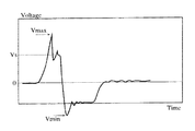
【0082】
このような効果を得るために、立ち上がり(図17(a)中においてTaで示される期間)の開始直後に印加される電圧値(図17(a)中においてVmaxで示される電圧最高値)は、放電開始電圧以上にすること、また「通常の維持電圧」(図17(a)中においてVsで示される電圧値)よりも50V以上高く設定することが好ましい。
【0083】
高電圧を印加する期間(図17(a)中においてTbで示される放電開始電圧以上の電圧が印加される期間)については、これを長くしすぎると、点灯させるべきでない放電セルにおいても絶縁破壊が起きて放電が発生したり、この期間に流れる電流によって消費電力が増大するという問題も生じ得るが、これを短時間に設定することによって、誘電体の絶縁破壊を回避できる。
【0084】
このような観点から、立ち上がり開始直後に印加する電圧値Vmaxを高く設定するほど、その印加時間Tbを短くすることが必要と考えられる。また、一般的には、この時間Tbを100ns以下に設定することが、当該期間に流れる電流を小さく抑える上で好ましく、更にこの時間を10ns以下に設定すれば、当該期間に流れる電流をほとんど0とすることができる点でより好ましいということが言える。
【0085】
なお、更に顕著な効果を得るために、立ち上がり開始直後に印加する電圧値Vmaxをかなり高く400V程度に設定すればよいと考えられるが、この場合、高電圧を印加する時間Tbをかなり短く(10〜20nsあるいはそれ以下に)設定する必要があるため、高電圧までシャープに立ち上げることのできる回路性能が要求されるものと考えられる。
【0086】
第3の特徴を付加したときの効果:
図17(a)の維持パルス波形においては、上記第2の特徴に加えて、走査電極群19aに正の維持パルスを印加する際に、立ち下がり直後の短い期間において、逆極性(負)パルスを短時間印加している。
図18(a)に示されるように、電極19aに正の維持パルスが印加されている時、電極19aから電極19bに向かう電界Eによって、放電空間20内に発生するイオンは電極(正イオンの場合は電極19b)に向かって移動する。
【0087】
そして、維持パルスが立ち下がった後においても、放電空間内を相手側の電極に向かうイオンが残るが、上述したようにこのイオンは発光にあまり寄与しないので、これが電極19bに到達すると無効電流となる。
これに対して、維持パルスの立ち下がり(図17(a)中においてTcで示される時点)直後に負パルスを印加すれば、図18(b)に示されるように電極19bから電極19aに向かう電界Eによって、電極19bに向かって移動する放電空間20内のイオンが、電極19bに到達することなく強制的に追い返される。そのため無効電流の発生は抑えられる。
【0088】
維持パルスの立ち下がり直後において印加する逆極性(負)パルスの電圧値(図11(a)中においてVminで示される電圧値)についても、絶対値が最高50V以上になるようにし、且つその印加時間は100ns以下に設定することが望ましく、更に短く10ns以下とすることが望ましい。
なお、維持パルスに第3の特徴を合わせる場合、従来と比べて放電の後半部分が消されるため、放電終了時において蓄積される壁電荷量が少なくなるとも考えられる。そして、放電終了時に蓄積される壁電荷量が少ないと、次に逆極性の維持パルスを印加する時に、放電が安定して開始されにくくなる可能性もある。
【0089】
従って、維持パルスに第3の特徴だけを付加する場合には、安定した放電を確保するために、維持電圧Vsを高めに設定することが望ましいと考えられる。
(維持パルスに特徴を付加する回路について)
このように立上がり時及び立ち下がり時に特徴を持った波形を維持パルスとして走査電極群19a及び維持電極群19bに印加するためには、図5,6に示す維持パルス発生器112a及び維持パルス発生器112bの各々に、図19に示すパルス合成回路を用いればよい。
【0090】
図19は、このような波形のパルスを発生するパルス合成回路のブロック図である。
このパルス合成回路は、トリガ信号に呼応してパルスを発生する第1パルス発生器231、第2パルス発生器232、第3パルス発生器233などから構成されている。
【0091】
第1パルス発生器231と第2パルス発生器232は、正電圧のパルスを発生するものであって、第2パルスの電圧は「維持電圧Vs」に設定されている。
第1パルス発生器231で発生する第1パルスは比較的幅狭のパルスである。一方、第2パルス発生器232で発生する第2パルスは比較的幅広の矩形波である。
【0092】
第3パルス発生器233は、負電圧の幅狭の第3パルスを発生するものであって、この第3パルスの立ち上がりのタイミングは、第2パルスの立ち下がりと一致するように設定されている。
第1〜第3パルス発生器231〜233は、フローティンググラウンド方式で直列に接続され、第1〜第3パルスの出力電圧が加算されるようになっている。
【0093】
そして、このパルス合成回路では、同期パルス生成部103から送られてくるトリガ信号に呼応して、以下のように各パルス発生器が動作してパルスを発生すると共に発生したパルスを合成して出力する。
図20は、上記パルス合成回路で第1パルス〜第3パルスが合成される様子を示す図である。
【0094】
先ず、同期パルス生成部103から第1パルス発生器231及び第2パルス発生器232にトリガ信号が送られて、第1パルス発生器231で第1パルスが、第2パルス発生器232で第2パルスが、ほぼ同時に立ち上げられる。従って、この立ち上がり開始直後においては、第1パルスの電圧と第2パルスの電圧が加算された高い電圧が出力される。
【0095】
第1パルスは短時間で立ち下がるので、第1パルスが立ち下がった後は、第2パルスだけが出力される。
そして、第2パルスが立ち下がる時に合わせて、同期パルス生成部103から第3パルス発生器233にトリガ信号が送られ、第3パルス発生器233で負電圧の第3パルスが立ち上げられる。そして、この第3パルスは短時間で立ち下げられる。従って、第2パルスの立ち下がり直後には負パルスが短時間出力される。
【0096】
この結果、図17(a)のような波形が合成されることになる。
なお、図19のパルス合成回路においては、第1パルス発生器231〜第3パルス発生器233の各出力電圧が加算されるような合成を行ったが、この合成回路の変形例として、第1パルス発生器231〜第3パルス発生器233を並列的に接続して、第1パルス〜第3パルスの中の電圧最大値が出力されるようにパルス合成を行ってもよい。
【0097】
但しこの場合、第1パルス発生器231で発生させる第1パルスの電圧値を、第2パルスよりも50V程度以上高く設定する必要があるので、第1パルス発生器231において、かなり高電圧で且つ時間幅の短いパルスを発生させなければならない点で、より高度な回路技術が必要と考えられる。
(維持パルスの立ち上がりの傾斜について)
本実施形態のように、維持パルスを印加する際に、立ち上がり開始直後の短時間に通常の維持電圧よりも高い電圧を短時間印加する場合、立ち上がり開始直後の短時間に、通常の維持電圧よりも大きい電圧変化幅が生じるので、それに伴い大きな電流が流れて発光効率が低下する傾向がある。
【0098】
従って、高発光効率を確保するために、立ち上がり部分の傾きをある程度緩やかに設定すればよいと考えられる。ただし、立ち上がり部分の中で通常の維持電圧を越えた高電圧の範囲で傾きを緩やかにすると、放電遅れを抑制する効果が損なわれてしまうことになる。
このような点を考慮すると、図17(a)に示されるパルス波形のように、立ち上がり部分の前半においては傾きを緩やかに設定して電流を抑え、後半においては傾きを大きくするのが好ましいということができる。
【0099】
また、逆極性で印加されるパルスの立ち下がり(図17(a)中においてTd )においても同様に、大きな電流が流れないよう、その傾きをある程度緩やかに設定することが好ましい。
維持パルスの立ち上がり時Taにおけるの傾きを調整するには、第1パルスの立ち上がりの傾きを調整するか、第1パルス及び第2パルス両方の立ち上がりの傾きを調整すればよく、第1パルス及び第2パルスの立ち上がりの傾きは、第1パルス発生器231及び第2パルス発生器232におけるRLC回路の時定数を調整することによって調整することができる。
【0100】
また、逆極性パルスの立ち下がり時Tdにおける傾きを調整するには、第3パルス発生器におけるRLC回路の時定数を調整することによって、第3パルスの立ち下がりの傾きを調整すればよい。
(本実施形態の変形例について)
なお、上記図17(a)では、各維持パルスの立ち上がり時Taにおいて、放電開始電圧以上の高電圧まで印加電圧が一気に上昇するような波形を示したが、立ち上がり時に一旦通常の維持電圧付近まで上昇し、少し遅れて高電圧まで上昇するような波形を用いても同様の効果を得ることができる。
【0101】
またこの外に、図21に示すような変形例も可能である。
この変形例は、正の維持パルスにおいて、その先縁から一定期間においてはそれ以降に印加される電圧より高電圧が印加され(第2の特徴)、且つ、立ち下がり直後において負パルスが印加されている(第3の特徴)点については、上記図17(a)と同様であるが、維持電圧Vsの期間はかなり短く、立ち下がり直後に印加される負パルスが印加される時間が長く、その波形も異なっている。即ち、図19の例では、維持パルスの立ち下がり直後に、負電圧Vminが短時間印加された後、弱い負電圧が比較的長時間印加されている。
【0102】
このような変形例を用いた場合においても、同様に発光効率を向上させることができる。
なお、当該変形例のような波形は、小容量電源(駆動回路)を用いたときに自然に発生することがあるし、また、回路の組み合わせによって、偶発的に発生する場合もある。
【0103】
また、本実施の形態では、各維持パルスの先縁直後に高電圧を印加する(第2の特徴)と共に後縁直後に逆極性パルスを印加する(第3の特徴)ことによって両特徴による効果を得る例を示したが、どちらか一方の特徴を維持パルスに加えるだけでもそれに相当する効果は得られる。
〔実施の形態4〕
本実施形態においても、放電維持期間に走査電極群19aと維持電極群19bとの間に印加される電圧波形の特徴については、上記実施の形態3と同様である。
【0104】
ただし、実施の形態3では、走査電極群19aに維持パルスを印加しているときには維持電極群19bは電圧を印加せず、維持電極群19bに維持パルスを印加しているときには走査電極群19aに電圧を印加しない例を示したが、本実施形態においては、走査電極群19a及び維持電極群19bの両方にパルスを印加し、その組み合わせによって、走査電極群19aと維持電極群19bとの間に印加される電圧波形に上記第2及び第3の特徴を形成している。
【0105】
即ち、図22〜図24の各タイミングチャートには、放電維持期間において、維持パルス発生器112a及び維持パルス発生器112bによって、走査電極群19a及び維持電極群19bの各々に、時間的に一部オーバラップするようにパルスが印加されている。そして、その結果、走査電極群19aと維持電極群19bとの間に電位差が発生する様子が示されているが、いづれにおいても、走査電極群19aと維持電極群19bとの間に生じる電位差波形が、上記第2、第3の特徴を有していることがわかる。
【0106】
図22の例では、走査電極群19aに正電圧の矩形波パルス(V1)が印加されるタイミングに合わせて、維持電極群19bには、この矩形波パルスの立ち上がりとほぼ同時に立ち上がる短時間幅の負パルス(−V2)と、この矩形波パルスの立ち下がりとほぼ同時に立ち下がる短時間幅の正パルス(V3)とが印加されている。この結果、走査電極群19aと維持電極群19bとの間には、立ち上がり直後の短時間に正の高電圧(V1+V2)が印加され、その後、しばらく正の維持電圧V1が印加され、その立ち下がり直後には、負のパルス(−V3)が短時間印加されることになる。
【0107】
一方、維持電極群19bに正の矩形波パルス(V1)が印加されるタイミングに合わせて、走査電極群19aには、この矩形波パルスの立ち上がりとほぼ同時に立ち上がる短時間幅の負パルス(−V2)と、この矩形波パルスの立ち下がりとほぼ同時に立ち下がる短時間幅の正パルス(V3)とが印加されている。
この結果、走査電極群19aと維持電極群19bとの間には、立ち上がり直後の短時間に負の高電圧−(V1+V2)が印加され、その後、しばらく負の維持電圧V1が印加され、その立ち下がり直後には、正パルス(V3)が短時間印加されることになる。
【0108】
本図の例では、各電極群19a,19bに印加するパルスは共に矩形波であるので、実施の形態1で用いたようなパルス合成回路を用いる必要はない。
図23の例では、走査電極群19aと維持電極群19bに対して、時間幅がほぼ同等で電圧値の異なる矩形波パルスが時間的に重なるように印加されている。走査電極群19aに対して高電圧V11(電圧Vmaxに相当する。)のパルスが印加され、維持電極群19bに対しては、立ち上がり及び立ち下がりのタイミングを短時間遅らせて低電圧V12(電圧Vmax−Vsに相当する。)のパルスが印加される。その結果、走査電極群19aと維持電極群19bとの間には、立ち上がり直後の短時間に正の高電圧(V11)が印加され、その後、しばらく正の維持電圧(V11−V12)が印加され、その立ち下がり直後には、負パルス(−V12)が短時間印加されることになる。
【0109】
一方、維持電極群19bに対して高電圧V1のパルスが印加される時には、走査電極群19aに対しては、立ち上がり及び立ち下がりのタイミングを短時間遅らせて低電圧V2のパルスが印加される。その結果、走査電極群19aと維持電極群19bとの間には、立ち上がり直後の短時間に負の高電圧(−V11)が印加され、その後、しばらく負の維持電圧(V12−V11)が印加され、その立ち下がり直後には、正パルス(V12)が短時間印加されることになる。
【0110】
本図の例では、維持パルス発生器112a及び維持パルス発生器112bにおいて、上記図22のように短い時間幅のパルスを印加する必要はなく、比較的時間幅の長いパルスを発生すればよいので、高電圧までシャープに立ち上げるという回路性能はあまり要求されず、回路に対する負担が少ない。
図24の例では、走査電極群19aに対して、t1時点〜t3時点の期間には正の高電圧V21が印加され、t3時点において電圧が立ち下がって、t3時点〜t4時点の期間には正の維持電圧V22が印加される。
【0111】
一方、維持電極群19bに対して、上記t1時点から少し遅れたt2時点から上記t3時点までの期間は正パルスV23が印加される。ここで、V23=V21−V22に設定されている。また、維持電極群19bに対して、t4時点〜t5時点の短い期間には正パルスV24が印加される。
この結果、電極19a−電極19b間の電位差について見ると、その立ち上がりの短時間(t1時点〜t2時点)においては、正の高電圧V21が印加され、その後の期間(t2時点〜t4時点)においては、正の維持電圧V22(=V21−V23)が印加され、立ち下がり後の短時間(t4時点〜t5時点)においては負パルス(−V24)が短時間印加されるような波形となっている。
【0112】
t6時点〜t10時点においては、走査電極群19aと維持電極群19bとが入れ代わって、上記t1時点〜t5時点と同様に印加される。そして、その結果、電極19a−電極19b間に、逆極性で同様の波形が形成される。
本図の例では、各電極19a,19bに高電圧V21を印加する期間が、短時間ではなく、且つ図12のように長時間ではないので、維持パルス発生器112a及び維持パルス発生器112bにおける負担が比較的少ない。
【0113】
なお、本例では、V21=V22+V23に設定されているため、t3時点における電極19a−電極19b間の電位差変化はないが、必らずしもこのように設定する必要はなく、t3時点において電極19a−電極19b間の電位差が多少変化しても同様の効果を奏する。
(実施の形態1〜4についてのバリエーション)
上記実施の形態1〜4では、放電維持期間におけるすべての維持パルスに対して、特徴を加えるようにしたが、良好な画像表示を行うことを主目的とする場合には、必ずしも放電維持期間におけるすべての維持パルスに対して特徴を加える必要はなく、一部の維持パルスに対して加えてもよい。
【0114】
但し、一般的に、放電維持期間において複数の維持パルスを連続的に印加する際、先頭の維持パルス印加時には特に放電遅れが発生しやすく、先頭の維持パルスにおいて放電が開始されれば2番目以降の維持パルスにおいても容易に放電が開始されるため、良好な画像表示を行うためには、少なくとも先頭の維持パルスに対しては上記特徴を加えるべきである。
【0115】
例えば、先頭の維持パルスに対して上記特徴を加え、2番目以降の維持パルスには、従来と同様の単純な矩形波を用いてもよい。
或は、走査電極群19aに正の維持パルスが印加される場合に上記特徴を加え、維持電極群19bに正の維持パルスが印加されるときには従来と同様の単純な矩形波を用いるようにしてもよい。
【0116】
この場合、すべての維持パルスに対して特徴を加える場合と比べて、発光効率を向上させる効果については劣るけれども、放電遅れの抑制についてはほぼ同等の効果を奏するものと考えられる。
上記実施の形態においては、交流面放電型のPDPを例にとって説明したが、対向放電型のPDPにおいても適用でき同様の効果を奏する。また、一般的に、書込パルスを印加することによって画像を書き込み、複数の放電セルに維持パルスを印加することによって放電維持を行うパネル表示装置であるならば同様に実施することができ同様の効果を奏する。
【0117】
【発明の効果】
以上説明したように、本発明は、維持パルスを印加する際に、その立ち上がりに要する時間に対して3倍の時間がピーク時点から経過するまでに立ち下がりが終了するような電流波形が形成されるよう、維持パルスの波形を規定することによって、無効電流を抑制し、発光効率を向上させることを可能とした。
【0118】
ここで、上記特徴を持つ電流波形は、維持パルスを印加する際に、当該維持パルスに次の第1〜第3のいずれかの特徴を加えることによって形成できる。
第1の特徴は、維持パルスの先縁(パルス立ち上がり)に先立って、当該維持パルスと逆極性のパルスを短時間印加することである。
第2の特徴は、維持パルスの先縁(パルスの立ち上がり)から一定期間において、それ以降に印加される電圧より絶対値において高電圧が印加されるような波形に設定することである。
【0119】
第3の特徴は、維持パルスの後縁(パルス立ち下がり)直後において、これと逆極性のパルスを印加することである。
なお、第1の特徴或は第2の特徴を維持パルスに加えると、放電遅れの抑制もなされる。
【図面の簡単な説明】
【図1】実施の形態にかかる交流面放電型PDPの見取図である。
【図2】上記PDPの電極マトリックスを示す図である。
【図3】上記PDPの駆動時におけるフレーム分割方法を示す図である。
【図4】実施の形態1において各電極にパルス印加するタイミングを示すチャートである。
【図5】実施の形態にかかるPDP駆動装置の構成を示すブロック図である。
【図6】図5中のスキャンドライバの構成を示すブロック図である。
【図7】図5中のデータドライバの構成を示すブロック図である。
【図8】維持パルス印加時における電流キャリアの動きを説明する図である。
【図9】維持パルス印加時に形成される電流波形を説明する図である。
【図10】維持パルス印加時に形成される電流波形と発光効率との関係を説明する図である。
【図11】実施の形態1にかかる維持パルス波形の一例を示す図、及び、従来から用いられている矩形波維持パルスの一例である。
【図12】維持パルス印加時における電流キャリアの動きを説明する図である。
【図13】実施の形態1にかかる維持パルスの特徴を形成するパルス合成回路のブロック図である。
【図14】上記パルス合成回路でパルスが合成される様子を示す図である。
【図15】実施の形態2で放電維持期間において各電極にパルスが印加される様子を示すタイミングチャートである。
【図16】実施の形態3において、各電極にパルス印加するタイミングを示すチャートである。
【図17】、 実施の形態3にかかる維持パルス波形の一例を示す図、及び、従来から用いられている矩形波維持パルスの一例である。
【図18】維持パルス印加時における電流キャリアの動きを説明する図である。
【図19】実施の形態3にかかる維持パルスの特徴を形成するパルス合成回路のブロック図である。
【図20】上記パルス合成回路でパルスが合成される様子を示す図である。
【図21】実施の形態3の一変形例にかかる維持パルスの特徴を示す図である。
【図22】実施の形態4において、放電維持期間において各電極にパルスを印加するタイミングの一例を示すチャートである。
【図23】実施の形態4において、放電維持期間において各電極にパルスを印加するタイミングの一例を示すチャートである。
【図24】実施の形態4において、放電維持期間において各電極にパルスを印加するタイミングの一例を示すチャートである。
【図25】従来例で各電極にパルスを印加するタイミングを示すチャートである。
【符号の説明】
11 前面基板
12 背面基板
13 誘電体層
14 データ電極
15 隔壁
16 蛍光体層
17 誘電体層
18 保護層
19a 走査電極
19b 維持電極
20 放電空間
100 駆動装置
112a 維持パルス発生器
112b 維持パルス発生器[0001]
TECHNICAL FIELD OF THE INVENTION
The present invention relates to a gas discharge panel display device and a method for driving a gas discharge panel used for image display of a computer, a television, and the like, and more particularly, to an AC device for writing an image by storing charges in a dielectric layer and emitting light by maintaining a discharge. Type PDP.
[0002]
[Prior art]
2. Description of the Related Art In recent years, in a display device used for a computer, a television, or the like, a gas discharge panel such as a plasma display panel (hereinafter, referred to as a PDP) is a large, thin, and lightweight gas discharge panel. Attention has been paid.
[0003]
The PDP is displayed as an image by selectively emitting light from discharge cells arranged in a matrix.
PDPs are roughly classified into a direct current type (DC type) and an alternating current type (AC type). At present, the AC type suitable for enlargement is mainly used.
In an AC type PDP, each discharge cell can originally express only two gradations of lighting or extinguishing. Therefore, one frame (one field) is divided into a plurality of subframes (subfields), and lighting / extinguishing in each subframe is performed. Are used to display an intermediate gray scale.
[0004]
In each sub-frame, an image is displayed by an ADS (Address Display-period Separation) method. That is, as shown in FIG. 25, each sub-frame is composed of a series of sequences including an initialization period, a writing period, a discharge sustaining period, and an erasing period. In the discharge sustaining period, an AC sustaining pulse is applied to all the discharge cells at once. The voltage of the sustain pulse applied at this time is set in a range (usually in the range of 150 to 200 V) such that the discharge is performed in the discharge cells in which the wall charges are accumulated and is not discharged in the other cells.
[0005]
The principle of this light emission is basically the same as that of a fluorescent lamp. By applying a sustain pulse to generate a normal glow discharge, ultraviolet rays (Xe resonance line, wavelength 147 nm) are generated from Xe, and the phosphor is excited to emit light. However, since the conversion efficiency of the discharge energy to ultraviolet light and the conversion efficiency of the phosphor to visible light are poor, it is difficult to obtain a high luminance like a fluorescent lamp.
[0006]
Like other displays, there is also a demand for higher definition in PDPs (for example, a high-definition television that is being put into practical use in recent years has a high-definition pixel with 1920 × 1080 full specifications). In such a high-definition PDP, the luminous efficiency tends to be further reduced.
[0007]
[Problems to be solved by the invention]
Under such a background, it is desired to improve the luminous efficiency (the luminous amount with respect to the input electric energy) in the PDP. To address this problem, for example, a technology for improving the luminous efficiency by improving the structure of the PDP and a technology for collecting a current (reactive current) that does not contribute to the emission of ultraviolet light have been developed. There is also a demand for a technique for reducing the amount.
[0008]
As shown in FIG. 25, a rectangular wave is generally used as the sustain pulse. Since the rise of this rectangular wave is sharper than that of a waveform such as a trigonometric function wave, basically, if a rectangular wave is used as the sustain pulse, discharge can be started in a relatively short time from the start of rise. Therefore, a relatively stable image can be displayed.
[0009]
However, when a sustain pulse is applied, a so-called "discharge delay" occurs in which the discharge is started with a considerable delay from its rise, with a certain probability. In particular, a discharge delay is likely to occur in the first sustain pulse applied during the sustain period.
Such “discharge delay” is a factor that degrades the quality of the displayed image. That is, although a large number of discharge cells are arranged in a PDP, if "discharge delay" occurs with a certain probability as described above, "discharge delay" occurs in some of the discharge cells to be turned on. As a result, lighting failure occurs and the image quality of the displayed image is degraded. Therefore, a technique for improving this is also desired.
[0010]
In view of such problems, a first object of the present invention is to improve the luminous efficiency by suppressing the generation of a reactive current when driving a gas discharge panel such as a PDP.
A second object is to improve the image quality by suppressing the occurrence of a discharge delay in the discharge sustaining period.
[0011]
[Means for Solving the Problems]
In order to achieve the first object, the present invention provides a method for applying a sustain pulse in which a fall is completed by a time three times as long as a rise time of the sustain pulse from a peak time. The waveform of the sustain pulse is defined so that the waveform is formed.
[0012]
In addition, in order to form a current waveform having the above characteristics, when applying the sustain pulse, any one of the following first to third characteristics is added to the sustain pulse.
A first feature is that a pulse having a polarity opposite to that of the sustain pulse is applied for a short time before the leading edge (pulse rise) of the sustain pulse.
The second feature is that the waveform is set so that a higher voltage is applied in a certain period from the leading edge of the sustain pulse (rising edge of the pulse) in absolute value than a voltage applied thereafter.
[0013]
The third feature is that a pulse having a polarity opposite to that of the sustain pulse is applied immediately after the trailing edge (falling pulse) of the sustain pulse.
When a current waveform having the above characteristics is formed, the reactive current is suppressed as compared with a case where a sustain pulse having a general waveform is applied, so that luminous efficiency can be improved.
[0014]
When the first to third characteristics are added to the sustain pulse, the following effects are exhibited in addition to the above-described improvement in the light emission efficiency.
When the first feature is added to the sustain pulse, when an opposite polarity pulse is initially applied, electrons move from one electrode to the other electrode, but before the pulse reaches the other electrode, the electron moves toward the other electrode. Starts to be returned to one electrode side.
[0015]
The reciprocation of electrons in the discharge space in the initial stage generates a large amount of charged particles (electrons and ions) contributing to light emission, thereby further improving the light emission efficiency.
In addition, since the charged particles reciprocate between the electrodes, a pilot spark of discharge is formed, and the discharge is started with high probability (EVOLUTION OF DISCHARGE) by the pilot spark, so that the second object, that is, the suppression of the discharge delay, is also performed. You.
[0016]
In order to reliably obtain the above effect, the voltage of the reverse polarity pulse is preferably set to have a voltage absolute value of 1.0 times or more with respect to the sustain pulse voltage. It is preferable to set the absolute value to 1.5 times or more.
Further, it is preferable to set this time to 100 ns or less for the period for applying the reverse polarity pulse.
[0017]
In particular, the time during which the voltage absolute value becomes 1.0 times or more the sustain pulse voltage is preferably set to 100 ns or less, and more preferably 50 ns or less.
Also when the second feature is added to the sustain pulse, a high voltage is applied for a certain period from the rise of each sustain pulse, so that the discharge is started reliably and the discharge delay is suppressed.
[0018]
In particular, if a high voltage equal to or higher than the discharge starting voltage of the discharge cell is applied during this fixed period, the effect is remarkable.
Here, it is preferable that a voltage higher than the sustain voltage applied thereafter by 50 V or more in absolute value be applied for a certain period from the leading edge of the sustain pulse.
[0019]
In general, when a high voltage is applied, dielectric breakdown of the dielectric layer and an increase in power consumption tend to occur, but the time for applying the high voltage (voltage equal to or higher than the discharge starting voltage of the discharge cell) is set to 100 ns or less or 10 ns or less. If the setting is made in a short time, dielectric breakdown of the dielectric layer and increase in power consumption can be avoided.
When the third feature is added to the sustain pulse, the reactive current caused by ions remaining in the discharge cells after the fall of the sustain pulse is suppressed.
[0020]
In other words, ions remaining in the discharge cells after the falling of the pulse are low-active and do not contribute to light emission. When the ions reach the electrodes, a reactive current is generated and the light emission efficiency is reduced. If the pulse is added with the third feature, the reactive current can be suppressed, and in this respect, it greatly contributes to the improvement of the luminous efficiency.
Here, it is preferable that the maximum value of the absolute voltage value of the reverse polarity pulse be 50 V or more.
[0021]
Further, the time for applying the reverse polarity pulse is set to 100 ns or less, and more preferably 10 ns or less.
By the way, in one discharge sustaining period, usually, a plurality of sustaining pulses are continuously applied to each discharge cell while switching the polarity. Therefore, in order to achieve a sufficient effect, it is preferable to apply the above-described waveform characteristics to all of the continuous sustain pulses, but apply the above-described waveform characteristics to only some of the sustain pulses. You may. However, also in this case, the characteristics of the waveform should be applied to at least the leading sustain pulse in the discharge sustain period.
[0022]
BEST MODE FOR CARRYING OUT THE INVENTION
(Overall description of display device)
First, the overall configuration of the PDP display device according to the present embodiment will be described.
This PDP display device is composed of an AC surface discharge type (AC type) PDP and its driving device. FIG. 1 is a sketch of this PDP.
[0023]
In this PDP, a
On the facing surface of the
[0024]
FIG. 2 is a diagram showing an electrode matrix of the PDP. The
[0025]
In a PDP for a single color display, a mixed gas mainly composed of neon is used as a discharge gas, and display is performed by emitting light in a visible region at the time of discharge. However, in a PDP for a color display as shown in FIG. A
[0026]
This PDP is driven using an in-frame time division gray scale display method.
FIG. 3 is a diagram illustrating a method of dividing one frame when expressing 256 gradations, where the horizontal direction indicates time, and the hatched portions indicate discharge sustaining periods.
For example, in the example of the division method shown in FIG. 3, one frame is composed of eight subframes, and the ratio of the sustaining periods of each subframe is 1, 2, 4, 8, 16, 32, 64. , 128, and 256 gradations can be expressed by the combination of the 8-bit binaries. In addition, in the NTSC system television video, since the video is composed of 60 frames per second, the time of one frame is set to 16.7 ms.
[0027]
In each subframe, an image is displayed on the PDP by the ADS method. That is, each subframe is configured by a series of sequences including an initialization period, a writing period, a discharge sustaining period, and an erasing period.
FIG. 4 is a timing chart when a pulse is applied to each electrode in one subframe in the present embodiment.
[0028]
In the initialization period, the state of all the discharge cells is initialized by applying an initialization pulse to the entire
During the writing period, a wall pulse is accumulated in a discharge cell to be turned on by applying a data pulse to a selected electrode in the
[0029]
In the discharge sustaining period, by applying a sustaining pulse while changing the polarity at once between the
As shown in FIG. 4, each sustain pulse has a unique waveform instead of a simple rectangular wave, which will be described in detail later.
[0030]
In the erasing period, the wall charges of the discharge cells are erased by applying a narrow erasing pulse to the
(Detailed description of driving device and driving method)
FIG. 5 is a block diagram showing a configuration of the
The
[0031]
The
[0032]
The
Specifically, the
[0033]
The synchronization
The
[0034]
FIG. 6 is a block diagram showing the configuration of the
The initialization pulse, the sustain pulse, and the erase pulse are applied to all the
Therefore, as shown in FIG. 6, the
[0035]
The
[0036]
Switches SW1 and SW2 are provided to selectively apply the outputs from the three
The sustain
[0037]
The
FIG. 7 is a block diagram showing the configuration of the
The
[0038]
The
[0039]
In such a
[0040]
In the initialization period, the switch SW1 of the
[0041]
During the writing period, the switch SW2 of the
[0042]
The pulse width (write pulse width) of the scan pulse and the data pulse is desirably set as short as possible in order to increase the driving speed. However, if the write pulse width is too short, a write failure easily occurs. Also, the pulse width usually needs to be set to about 1.0 μsec or more due to circuit restrictions.
In the discharge sustaining period, the switch SW1 of the
[0043]
As a result, in the discharge cells in which the wall charges are accumulated during the writing period, a discharge occurs when the potential on the dielectric layer surface exceeds the discharge starting voltage, and ultraviolet light is emitted in the discharge cells along with the sustain discharge. This is converted into visible light by the phosphor layer, thereby emitting visible light corresponding to the color of the phosphor layer.
During the erasing period, the switch SW1 of the
[0044]
<Pulse waveform during discharge sustain period>
First, an outline will be given of the characteristics of the waveform of the sustain pulse applied between the
According to the present invention, when a sustain pulse is applied, a current waveform is formed that has a characteristic that the fall ends before the time required for the rise to the peak reaches three times the elapsed time from the peak time. Thus, the waveform of the sustain pulse was adjusted.
[0045]
That is, when the sustain pulse is applied, when the time that is three times longer than the time required for the rise has elapsed from the peak time, the current is adjusted to be extremely small, thereby suppressing the reactive current and improving the luminous efficiency. I tried to make it.
It has also been found that the current waveform having the above characteristics can be obtained by adding any of the following first to third characteristics when applying the sustain pulse.
[0046]
First feature: Prior to the leading edge (pulse rise) of the sustain pulse, a pulse of the opposite polarity to the sustain pulse is applied for a short time.
Second feature: The waveform is set so that a higher voltage is applied in a certain period from the leading edge of the sustain pulse (rising edge of the pulse) in absolute value than the voltage applied thereafter.
[0047]
Third feature: Immediately after the trailing edge (falling pulse) of the sustain pulse, a pulse of the opposite polarity is applied.
In addition, when the sustain pulse is applied, by adding any one of the above-described first to third features, the above-described feature (the time that is three times as long as the time required for the rise to the peak elapses from the peak time) It was also experimentally confirmed that a current waveform having a time until the end of the current) was obtained.
[0048]
Next, the reason why the generation of the current waveform having the above characteristics can suppress the reactive current will be described below.
Here, a mechanism in which light emission occurs in the discharge space will be considered by taking a case where a positive sustain pulse is applied to the
When a positive sustain pulse (+ V) is applied to the
[0049]
Here, since the electrons (e) and the ions (Xe +) in the discharge space are regarded as current carriers, when the electrons or ions generated in the
By the way, comparing the moving speeds of the electron and the ion in the electric field, the moving speed of the electron is much higher than that of the ion due to the difference in mass (the speeds of both are different by several orders of magnitude).
[0050]
Therefore, as shown in FIG. 9A, the peak of the current (current due to the electrons) mainly due to the electrons reaching the
Here, the current at an early time, which is considered to be due to electrons moving at high speed in the discharge space, greatly contributes to light emission, whereas the current at a late time, which is considered to be due to ions moving at low speed, has a small contribution to light emission, and is therefore slow. If the current at the time is suppressed, the luminous efficiency can be improved.
[0051]
Further, as described above, when the above-described first to third features are added when the sustain pulse is applied, “the time that is three times as long as the time required for the rise to the peak to elapse from the peak time” elapses. Since it is known that a current waveform having the characteristic of “falling ends” can be formed, it can be said that “current by electrons” also has the characteristic of this waveform.
[0052]
Therefore, when a current waveform having the above characteristics is formed, “current due to ions” that does not contribute to light emission is suppressed, and light emission efficiency is improved.
The above contents are supported by the following experimental results.
FIG. 9B shows a voltage waveform and a current waveform observed when a rectangular pulse is applied by a drive circuit between display electrodes of an AC type gas discharge panel, as shown in FIG. 9C. The measurement is performed by incorporating a voltmeter and an ammeter (current probe) in the wiring connecting the drive circuit and the display electrode.
[0053]
The fact that the current waveform in FIG. 9B substantially matches the sum of the two current waveforms shown in FIG. 9A supports the above description.
FIG. 10A shows a current waveform and a light emission luminance waveform observed when a pulse is applied by a drive circuit between display electrodes of an AC gas discharge panel. In the current waveform in FIG. 10A, a sharp peak A1 is seen at an early time and a gentle peak A2 is seen at a late time. On the other hand, in the emission luminance waveform, a sharp peak B1 is clearly seen at an early time, but a gentle peak B2 at a late time is hardly seen. Note that this emission luminance waveform is similar to the waveform of the current caused by electrons in FIG.
[0054]
FIG. 10B is a waveform of the light emission efficiency derived from the voltage waveform and the current waveform of FIG. 9B and the light emission luminance waveform of FIG. 10A. This luminous efficiency waveform indicates a change in luminous efficiency when the sustain pulse is applied (how the ratio of the luminous luminance to the power supplied every minute time changes).
FIG. 10 (c) shows the luminous efficiency waveform of FIG. 10 (b) superimposed on the current waveform of the electrons of FIG. 9 (a). FIG. 10C shows that the peak of the current waveform due to the electrons and the peak of the luminous efficiency waveform overlap, which indicates that high luminous efficiency can be obtained at the time when the current due to the electrons flows.
[0055]
That is, as shown in FIG. 10C, if a current waveform close to the peak waveform of “current due to electrons” is formed when the sustain pulse is applied, power is supplied intensively at a time when the luminous efficiency is high. Therefore, it can be seen that high luminous efficiency can be obtained.
The first to third features and effects will be more specifically described in the following first to fourth embodiments.
[0056]
[Embodiment 1]
As shown in FIG. 4, in the present embodiment, positive sustain pulses are alternately applied to scan
Hereinafter, the case where the sustain pulse is applied to the
[0057]
First, when a positive sustain pulse is applied to the
Here, the value of the sustain voltage Vs is a voltage value set within a range such that discharge is performed in a discharge cell in which wall charges are accumulated at the time of addressing and is not discharged in a discharge cell in which wall charges are not accumulated. , PDP panel design (discharge cell size, electrode width, dielectric layer thickness, etc.).
[0058]
Generally, the sustain voltage Vs is set at a voltage lower than the discharge start voltage of the discharge cell (a range from the discharge start voltage -50 V to the discharge start voltage). It can be set lower than a reasonable value.
In addition, the discharge starting voltage in a PDP can be measured as follows.
[0059]
While visually observing the PDP, the voltage applied to the PDP from the panel driving device is gradually increased, and the applied voltage when one or a specified number (for example, three) or more of the discharge cells of the PDP starts to light up is increased. Read and record this as the firing voltage.
(Description of effects of the present embodiment)
FIG. 11A shows an example of the sustain pulse waveform according to the present embodiment. The basic part of the sustain pulse is a rectangular wave, but when the sustain pulse is applied, the polarity is reversed before the rise of the sustain pulse. A pulse is applied for a short time. On the other hand, FIG. 11B shows an example in which the sustain pulse is a general rectangular wave.
[0060]
In the case where a simple rectangular wave is used as shown in FIG. 11B, when a sustain pulse is applied to the discharge cells, fast electrons initially generated in the discharge space do not contribute to light emission, and do not contribute to light emission. From the first electrode to the other electrode.
On the other hand, when a positive sustain pulse is applied to the
[0061]
As described above, while the electrons reciprocate in the discharge space, they frequently collide with the gas particles, so that many excited atoms and the like that contribute to light emission are generated. Therefore, the luminous efficiency is improved as compared with the case where a simple rectangular wave is applied as shown in FIG.
In addition, when a sustain pulse composed of a general rectangular wave is applied, a discharge delay may occur due to a voltage drop at the time of rising. It is considered that this discharge delay occurs because a voltage suddenly starts flowing at the rise of the sustain pulse, causing a voltage drop, and it takes time until the potential rises again.
[0062]
On the other hand, if the reverse polarity pulse is added immediately before the start of the application of the sustain pulse, the electrons reciprocate as described above, so that the collision with the gas particles frequently occurs, and the pilot flame is surely formed. Discharge can be started with high probability, and discharge delay can be suppressed.
Therefore, even if the sustain voltage Vs is set relatively low, the discharge is reliably performed. That is, the sustain voltage Vs in FIG. 11A is set lower than the sustain voltage V in FIG. 11B. Image display is possible.
[0063]
When the maintenance voltage is set to a lower value in this manner, the “current due to ions” can be reduced, and from this point, it can be said that the luminous efficiency is improved compared to the related art.
In order to obtain such an effect, the voltage value of the negative pulse (the voltage indicated by Vmin in FIG. 11A) applied before the rising (the period indicated by Ta in FIG. 11A) is It is preferable to set the absolute value of the voltage to be equal to or greater than the sustain voltage Vs or the discharge start voltage, and it is more preferable to set the absolute value of the voltage to 1.5 times or more.
[0064]
If the period during which the negative pulse is applied prior to the rise (the period indicated by Tb in FIG. 11A) is too long, there may be a problem that power consumption increases due to the current flowing during this period. . In particular, if the period in which the voltage absolute value is larger than the sustain voltage Vs (or the discharge start voltage) (the period indicated by Tc in FIG. 11A) is too long in the period Tb, the current flowing in this period Although the power consumption increases, by setting this to a short time, the increase in the power consumption can be suppressed to a slight level.
[0065]
From such a viewpoint, it is considered necessary to set the application time shorter as the absolute value of the voltage Vmin of the reverse polarity pulse to be applied is set larger. Generally, it is preferable to set this period Tc to 100 ns or less.
For example, when the gap between the
[0066]
Further, it is more preferable that the time during which the voltage absolute value is equal to or higher than the discharge starting voltage is set to 50 ns or less in the period in which the negative pulse is applied, since the current flowing in the period can be almost zero. I can say.
(About the circuit that applies a reverse polarity pulse to the sustain pulse)
In order to apply a reverse polarity pulse to the sustain pulse, a pulse synthesis circuit as shown in FIG. 13 may be used for each of the sustain
[0067]
FIG. 13 is a block diagram of a pulse synthesis circuit that forms such a pulse waveform.
The pulse synthesizing circuit includes a
The
[0068]
The rising timing of the second pulse is set so as to substantially coincide with the falling of the first pulse.
The first and
Then, in this pulse synthesizing circuit, in response to the trigger signal sent from the synchronizing
[0069]
FIG. 14 is a diagram showing how the first pulse and the second pulse are synthesized by the pulse synthesis circuit.
First, a trigger signal is sent from the
[0070]
As a modification of the pulse synthesizing circuit shown in FIG. 13, a
(About the rising slope of the reverse polarity pulse)
By the way, when the reverse polarity pulse is applied prior to the sustain pulse, if the slope at the rising portion of the reverse polarity pulse is too large, that is, if the applied voltage is changed in a very short time with a large voltage change width, the applied voltage becomes large. There is a tendency for the luminous efficiency to decrease due to the flow of current.
[0071]
Therefore, in order to secure high luminous efficiency, it is considered that the slope of the rising portion of the reverse polarity pulse should be set to a moderate degree. However, if the slope is gradual in the range where the absolute value exceeds the sustain voltage Vs in the rising portion, the effect of suppressing the discharge delay will be impaired.
Considering such points, as in the pulse waveform shown in FIG. 11A, the gradient is set gently in the first half of the rising portion of the reverse polarity pulse to suppress the current, and the gradient is increased in the second half. Is preferred.
[0072]
In order to adjust the slope at the time of the rising of the reverse polarity pulse, the slope of the rising of the first pulse may be adjusted, which may be adjusted by adjusting the time constant of the RLC circuit in the
[Embodiment 2]
Also in the present embodiment, the characteristics of the sustain pulse applied between
[0073]
However, in the first embodiment, in the discharge sustaining period, the voltage is applied to only one of the electrode groups at a moment, that is, when the sustain pulse is applied to the
[0074]
FIG. 15 shows that the sustain
[0075]
In the example of FIG. 15, a rectangular wave pulse (V1) of a positive voltage is applied to the sustaining
[0076]
On the other hand, a rectangular wave pulse (V1) of a positive voltage is applied to the
[0077]
As a result, a positive pulse (-V1) is applied between the
As described above, in the example of this figure, since the pulses applied to each of the
[0078]
[Embodiment 3]
As shown in FIG. 16, in the present embodiment, positive sustain pulses are alternately applied to scan
[0079]
Hereinafter, the case where the sustain pulse is applied to the
(Explanation of the effect of the sustain pulse waveform of the present embodiment)
FIG. 17A is an example of a sustain pulse waveform according to the present embodiment. In a positive sustain pulse, a basic portion is a rectangular wave, but is applied after a certain period from the leading edge thereof. A voltage higher than the voltage is applied (second feature), and a negative pulse is applied immediately after the fall of the sustain pulse (third feature). On the other hand, FIG. 17B is an example of a general rectangular wave sustain pulse.
[0080]
The second feature and the third feature may be added independently, and each has the following effects.
Effect of adding the second feature:
When a sustain pulse composed of a simple rectangular wave is applied as shown in FIG. 17 (b), a discharge delay is likely to occur due to a voltage drop at the time of rising. On the other hand, as shown in FIG. When a high voltage is applied for a certain period from the leading edge of the pulse, the above-described voltage drop is suppressed, so that it is possible to avoid an increase in the discharge start delay.
[0081]
Therefore, even if the sustain voltage Vs is set relatively low, the discharge is reliably performed. That is, in the waveform of FIG. 17A, the normal sustain voltage Vs is set to be considerably lower than the waveform of FIG. 17B. However, even if such a waveform is used, the discharge delay increases. However, it is possible to display images satisfactorily.
Thus, when the sustain voltage Vs is set low, it can be said that the luminous efficiency is improved in that the “current due to ions” can be reduced.
[0082]
In order to obtain such an effect, the voltage value (the maximum voltage value indicated by Vmax in FIG. 17A) applied immediately after the start of the rise (the period indicated by Ta in FIG. 17A) is It is preferable that the voltage is set to be equal to or higher than the discharge starting voltage, and set to be 50 V or higher than the “normal sustain voltage” (the voltage value indicated by Vs in FIG. 17A).
[0083]
For a period during which a high voltage is applied (a period during which a voltage equal to or higher than the discharge starting voltage indicated by Tb in FIG. 17A) is applied, if this is set too long, dielectric breakdown will occur even in discharge cells that should not be turned on. May occur, and a problem may arise in that power consumption increases due to current flowing during this period, but by setting this to a short time, dielectric breakdown of the dielectric can be avoided.
[0084]
From such a viewpoint, it is considered that the higher the voltage value Vmax applied immediately after the start of rising, the shorter the application time Tb is required. In general, it is preferable to set the time Tb to 100 ns or less in order to keep the current flowing in the period small, and if the time Tb is set to 10 ns or less, the current flowing in the period is almost zero. Can be said to be more preferable in that
[0085]
In order to obtain a more remarkable effect, it is considered that the voltage value Vmax applied immediately after the start of the rise may be set to a considerably high value of about 400 V. In this case, the time Tb for applying the high voltage is considerably shortened (10 (20 ns or less), it is considered that a circuit performance capable of sharply starting up to a high voltage is required.
[0086]
Effect of adding the third feature:
In the sustain pulse waveform of FIG. 17A, in addition to the second feature, when a positive sustain pulse is applied to the
As shown in FIG. 18A, when a positive sustain pulse is applied to the
[0087]
Even after the sustain pulse falls, ions remaining in the discharge space toward the other electrode remain. However, as described above, these ions do not contribute much to light emission. Become.
On the other hand, if a negative pulse is applied immediately after the fall of the sustain pulse (at the time indicated by Tc in FIG. 17A), the electrode goes from the
[0088]
The voltage value of the reverse polarity (negative) pulse applied immediately after the fall of the sustain pulse (the voltage value indicated by Vmin in FIG. 11A) is also set to have an absolute value of 50 V or more at the maximum, and to apply the voltage. The time is desirably set to 100 ns or less, and more desirably 10 ns or less.
When the third feature is combined with the sustain pulse, since the latter half of the discharge is erased compared to the conventional case, it is considered that the amount of wall charges accumulated at the end of the discharge is reduced. If the amount of wall charges accumulated at the end of the discharge is small, the discharge may not be stably started when the next sustain pulse of the opposite polarity is applied.
[0089]
Therefore, when only the third feature is added to the sustain pulse, it is considered desirable to set the sustain voltage Vs higher in order to secure a stable discharge.
(About the circuit that adds features to the sustain pulse)
In order to apply a waveform having characteristics at the time of rising and falling as a sustain pulse to the
[0090]
FIG. 19 is a block diagram of a pulse synthesis circuit that generates a pulse having such a waveform.
This pulse synthesizing circuit includes a
[0091]
The
The first pulse generated by the
[0092]
The third pulse generator 233 generates a third pulse having a narrow negative voltage, and the rising timing of the third pulse is set to coincide with the falling of the second pulse. .
The first to
[0093]
Then, in this pulse synthesizing circuit, in response to the trigger signal sent from the synchronizing
FIG. 20 is a diagram showing how the first to third pulses are synthesized by the above-described pulse synthesis circuit.
[0094]
First, a trigger signal is sent from the
[0095]
Since the first pulse falls in a short time, only the second pulse is output after the first pulse falls.
Then, at the same time as the falling of the second pulse, a trigger signal is sent from the synchronizing
[0096]
As a result, a waveform as shown in FIG.
In the pulse synthesizing circuit shown in FIG. 19, the synthesizing is performed such that the output voltages of the first to
[0097]
However, in this case, it is necessary to set the voltage value of the first pulse generated by the
(About the rising slope of the sustain pulse)
As in the present embodiment, when a sustain pulse is applied, when a voltage higher than the normal sustain voltage is applied for a short time in a short time immediately after the start of the rise, when the voltage is higher than the normal sustain voltage in a short time immediately after the start of the rise. Since a large voltage change width occurs, a large current flows along with this, and the luminous efficiency tends to decrease.
[0098]
Therefore, in order to secure high luminous efficiency, it is considered that the slope of the rising portion should be set to some degree gently. However, if the slope is made gentle within a high voltage range exceeding the normal sustain voltage in the rising portion, the effect of suppressing the discharge delay will be impaired.
Considering such points, it is preferable to set a gentle slope in the first half of the rising portion to suppress the current and increase the slope in the second half, as in the pulse waveform shown in FIG. be able to.
[0099]
Similarly, at the falling edge of the pulse applied with the opposite polarity (Td in FIG. 17A), it is preferable to set the slope to a certain degree so that a large current does not flow.
To adjust the slope of the sustain pulse at the rising edge Ta, the rising slope of the first pulse may be adjusted, or the rising slopes of both the first pulse and the second pulse may be adjusted. The rising slope of the two pulses can be adjusted by adjusting the time constant of the RLC circuit in the
[0100]
In addition, in order to adjust the slope at the falling time Td of the reverse polarity pulse, the falling slope of the third pulse may be adjusted by adjusting the time constant of the RLC circuit in the third pulse generator.
(About a modification of the present embodiment)
In FIG. 17A, a waveform is shown in which the applied voltage rises at a stroke to a high voltage equal to or higher than the discharge starting voltage at the rising time Ta of each sustain pulse. The same effect can be obtained by using a waveform that rises and rises to a high voltage with a slight delay.
[0101]
In addition, a modified example as shown in FIG. 21 is also possible.
In this modification, in a positive sustain pulse, a voltage higher than a voltage applied thereafter is applied for a certain period from the leading edge thereof (second characteristic), and a negative pulse is applied immediately after the fall. (Third feature) is the same as FIG. 17A, except that the period of the sustain voltage Vs is considerably short, and the time for applying the negative pulse applied immediately after the fall is long. Their waveforms are also different. That is, in the example of FIG. 19, immediately after the falling of the sustain pulse, the negative voltage Vmin is applied for a short time, and then the weak negative voltage is applied for a relatively long time.
[0102]
Even when such a modified example is used, the luminous efficiency can be similarly improved.
Note that the waveform as in the modified example may occur naturally when a small-capacity power supply (drive circuit) is used, or may occur accidentally depending on a combination of circuits.
[0103]
Further, in the present embodiment, by applying a high voltage immediately after the leading edge of each sustain pulse (second feature) and applying a reverse polarity pulse immediately after the trailing edge (third feature), the effect of both features is achieved. Has been described, but an effect equivalent to that can be obtained by simply adding one of the features to the sustain pulse.
[Embodiment 4]
Also in the present embodiment, the characteristics of the voltage waveform applied between the
[0104]
However, in the third embodiment, when a sustain pulse is applied to scan
[0105]
That is, in each of the timing charts of FIGS. 22 to 24, in the sustaining period, the sustain
[0106]
In the example of FIG. 22, the sustain
[0107]
On the other hand, in synchronism with the timing at which the positive rectangular wave pulse (V1) is applied to the sustain
As a result, a negative high voltage − (V1 + V2) is applied between the
[0108]
In the example of this figure, since the pulses applied to each of the
In the example of FIG. 23, rectangular wave pulses having substantially the same time width and different voltage values are applied to the
[0109]
On the other hand, when the pulse of the high voltage V1 is applied to the sustain
[0110]
In the example of this drawing, the sustain
In the example of FIG. 24, a positive high voltage V21 is applied to the
[0111]
On the other hand, a positive pulse V23 is applied to the sustain
As a result, regarding the potential difference between the
[0112]
From time t6 to time t10, the
In the example of this figure, since the period during which the high voltage V21 is applied to each of the
[0113]
In this example, since V21 = V22 + V23 is set, there is no change in the potential difference between the
(Variations of
In the first to fourth embodiments, a feature is added to all the sustain pulses in the discharge sustain period. However, when the main purpose is to perform good image display, the feature is not necessarily required in the discharge sustain period. It is not necessary to add a feature to every sustain pulse, and it may be added to some sustain pulses.
[0114]
However, in general, when a plurality of sustain pulses are successively applied during the discharge sustain period, a discharge delay is particularly likely to occur when the first sustain pulse is applied. Since the discharge is easily started even with the sustain pulse of, the above-mentioned feature should be added to at least the first sustain pulse in order to display a good image.
[0115]
For example, the above-described characteristics may be added to the first sustain pulse, and a simple rectangular wave similar to the conventional one may be used for the second and subsequent sustain pulses.
Alternatively, when the positive sustain pulse is applied to the
[0116]
In this case, although the effect of improving the luminous efficiency is inferior to the case where the feature is added to all the sustain pulses, it is considered that the effect of suppressing the discharge delay is almost the same.
In the above-described embodiment, an AC surface discharge type PDP has been described as an example. However, the present invention can be applied to a facing discharge type PDP and has the same effect. In general, a panel display device that writes an image by applying a write pulse and sustains a discharge by applying a sustain pulse to a plurality of discharge cells can be similarly implemented. It works.
[0117]
【The invention's effect】
As described above, according to the present invention, when the sustain pulse is applied, the current waveform is formed such that the fall is completed before the time required for the rise is three times as long as the peak time. Thus, by defining the waveform of the sustain pulse, it is possible to suppress the reactive current and improve the luminous efficiency.
[0118]
Here, the current waveform having the above characteristics can be formed by adding any of the following first to third characteristics to the sustain pulse when applying the sustain pulse.
A first feature is that a pulse having a polarity opposite to that of the sustain pulse is applied for a short time before the leading edge (pulse rise) of the sustain pulse.
The second feature is that the waveform is set so that a higher voltage is applied in a certain period from the leading edge of the sustain pulse (rising edge of the pulse) in absolute value than a voltage applied thereafter.
[0119]
The third feature is that a pulse having a polarity opposite to that of the sustain pulse is applied immediately after the trailing edge (falling pulse) of the sustain pulse.
In addition, when the first characteristic or the second characteristic is added to the sustain pulse, the discharge delay is suppressed.
[Brief description of the drawings]
FIG. 1 is a sketch of an AC surface discharge type PDP according to an embodiment.
FIG. 2 is a view showing an electrode matrix of the PDP.
FIG. 3 is a diagram showing a frame dividing method at the time of driving the PDP.
FIG. 4 is a chart showing a timing of applying a pulse to each electrode in the first embodiment.
FIG. 5 is a block diagram illustrating a configuration of a PDP driving device according to an embodiment.
FIG. 6 is a block diagram illustrating a configuration of a scan driver in FIG. 5;
FIG. 7 is a block diagram illustrating a configuration of a data driver in FIG. 5;
FIG. 8 is a diagram illustrating movement of a current carrier when a sustain pulse is applied.
FIG. 9 is a diagram illustrating a current waveform formed when a sustain pulse is applied.
FIG. 10 is a diagram illustrating a relationship between a current waveform formed when a sustain pulse is applied and luminous efficiency.
FIG. 11 is a diagram showing an example of a sustain pulse waveform according to the first embodiment, and an example of a rectangular wave sustain pulse conventionally used.
FIG. 12 is a diagram illustrating the movement of a current carrier when a sustain pulse is applied.
FIG. 13 is a block diagram of a pulse synthesizing circuit that forms a feature of the sustain pulse according to the first exemplary embodiment;
FIG. 14 is a diagram illustrating a state in which pulses are synthesized by the pulse synthesis circuit.
FIG. 15 is a timing chart showing a state in which a pulse is applied to each electrode during a sustain period in the second embodiment.
FIG. 16 is a chart showing a timing of applying a pulse to each electrode in the third embodiment.
FIG. 17 is a diagram showing an example of a sustain pulse waveform according to the third embodiment, and is an example of a rectangular wave sustain pulse conventionally used.
FIG. 18 is a diagram illustrating movement of a current carrier when a sustain pulse is applied.
FIG. 19 is a block diagram of a pulse synthesizing circuit that forms a feature of a sustain pulse according to the third embodiment;
FIG. 20 is a diagram illustrating a state in which pulses are synthesized by the pulse synthesis circuit.
FIG. 21 is a diagram showing characteristics of a sustain pulse according to a modification of the third embodiment.
FIG. 22 is a chart showing an example of a timing at which a pulse is applied to each electrode during a sustain period in the fourth embodiment.
FIG. 23 is a chart showing an example of a timing at which a pulse is applied to each electrode during a sustain period in the fourth embodiment.
FIG. 24 is a chart showing an example of a timing at which a pulse is applied to each electrode during a sustain period in
FIG. 25 is a chart showing a timing of applying a pulse to each electrode in a conventional example.
[Explanation of symbols]
11 Front board
12 Back substrate
13 Dielectric layer
14 Data electrode
15 Partition wall
16 phosphor layer
17 Dielectric layer
18 Protective layer
19a scanning electrode
19b sustain electrode
20 Discharge space
100 drive
112a Sustain pulse generator
112b Sustain pulse generator
Claims (8)
前記複数の放電セルに書込パルスを印加することによって画像を書き込み、前記複数の放電セルに維持パルスを印加することによって放電維持を行う駆動回路とを備え、放電維持期間において前記放電パネルが画像を表示するパネル表示装置であって、
前記駆動回路は、更に、異なる位相で同一波形の維持パルスを前記維持電極と走査電極に交互に印加するとともに、少なくとも先頭の維持パルスの先縁に連続して先立つ一定期間において、当該維持パルスとは逆極性で予備放電させられる電位レベルのパルスを前記維持電極と走査電極に交互に印加することを特徴とするパネル表示装置。A gas discharge panel in which a plurality of discharge cells are arranged in a matrix between a pair of substrates having sustain electrodes, scan electrodes, and data electrodes ;
A driving circuit for writing an image by applying a write pulse to the plurality of discharge cells and maintaining a discharge by applying a sustain pulse to the plurality of discharge cells; A panel display device for displaying
The drive circuit may further provide different with the sustain pulses of the phase in the same waveform is applied alternately to the sustain electrode and the scan electrodes, a certain period prior to continuous leading edge of at least the beginning of the sustain pulse, and the sustain pulse Wherein a pulse of a potential level preliminarily discharged with a reverse polarity is alternately applied to the sustain electrode and the scan electrode .
前記複数の放電セルに書込パルスを印加することによって画像を書き込み、前記複数の放電セルに維持パルスを印加することによって放電維持を行う駆動回路とを備え、放電維持期間において前記ガス放電パネルが画像を表示するパネル表示装置であって、
前記駆動回路によって放電セルに印加される少なくとも先頭の維持パルスは、
当該維持パルスの先縁から一定期間における電圧が、当該一定期間経過後から維持パルスの後縁までの期間における電圧より絶対値が高く、絶対値において放電セルの放電開始電圧より高く、 前記駆動回路が前記一定期間経過後から維持パルスの後縁までの期間において放電セルに印加する電圧は、絶対値において放電セルの放電開始電圧より低く、前記放電開始電圧より高い電圧を印加する時間は、100ns以下である
ことを特徴とするパネル表示装置。A gas discharge panel in which a plurality of discharge cells are arranged in a matrix between a pair of substrates;
A driving circuit for writing an image by applying a write pulse to the plurality of discharge cells and maintaining a discharge by applying a sustain pulse to the plurality of discharge cells; A panel display device that displays an image,
At least the first sustain pulse applied to the discharge cells by the driving circuit is
The voltage in a certain period from the leading edge of the sustain pulse has a higher absolute value than the voltage in a period from the elapse of the certain period to the trailing edge of the sustain pulse, and the absolute value is higher than the discharge start voltage of the discharge cell, The voltage applied to the discharge cell during the period from the elapse of the certain period to the trailing edge of the sustain pulse is lower than the discharge start voltage of the discharge cell in absolute value, and the time for applying the voltage higher than the discharge start voltage is 100 ns. A panel display device characterized by the following .
各維持パルスの後縁から一定期間において、当該維持パルスとは逆極性のパルスを前記放電セルに印加することを特徴とする請求項6記載のパネル表示装置。The driving circuit further includes:
7. The panel display device according to claim 6 , wherein a pulse having a polarity opposite to that of the sustain pulse is applied to the discharge cells for a predetermined period from a trailing edge of each sustain pulse.
Priority Applications (1)
| Application Number | Priority Date | Filing Date | Title |
|---|---|---|---|
| JP2001068720A JP3595273B2 (en) | 2000-03-13 | 2001-03-12 | Panel display device |
Applications Claiming Priority (3)
| Application Number | Priority Date | Filing Date | Title |
|---|---|---|---|
| JP2000-68707 | 2000-03-13 | ||
| JP2000068707 | 2000-03-13 | ||
| JP2001068720A JP3595273B2 (en) | 2000-03-13 | 2001-03-12 | Panel display device |
Publications (2)
| Publication Number | Publication Date |
|---|---|
| JP2001331148A JP2001331148A (en) | 2001-11-30 |
| JP3595273B2 true JP3595273B2 (en) | 2004-12-02 |
Family
ID=26587319
Family Applications (1)
| Application Number | Title | Priority Date | Filing Date |
|---|---|---|---|
| JP2001068720A Expired - Fee Related JP3595273B2 (en) | 2000-03-13 | 2001-03-12 | Panel display device |
Country Status (1)
| Country | Link |
|---|---|
| JP (1) | JP3595273B2 (en) |
Families Citing this family (4)
| Publication number | Priority date | Publication date | Assignee | Title |
|---|---|---|---|---|
| US20060022904A1 (en) * | 2004-07-29 | 2006-02-02 | Lg Electronics Inc. | Plasma display apparatus applying sustain pulse and driving method thereof |
| JP4699146B2 (en) * | 2004-09-07 | 2011-06-08 | エルジー エレクトロニクス インコーポレイティド | Plasma display device and driving method thereof |
| KR100747168B1 (en) * | 2005-02-18 | 2007-08-07 | 엘지전자 주식회사 | Driving Apparatus and Method for Plasma Display Panel |
| KR100673469B1 (en) | 2005-09-16 | 2007-01-24 | 엘지전자 주식회사 | Plasma display apparasute |
-
2001
- 2001-03-12 JP JP2001068720A patent/JP3595273B2/en not_active Expired - Fee Related
Also Published As
| Publication number | Publication date |
|---|---|
| JP2001331148A (en) | 2001-11-30 |
Similar Documents
| Publication | Publication Date | Title |
|---|---|---|
| JP4015884B2 (en) | Plasma display apparatus and driving method thereof | |
| TW418380B (en) | Method for driving a plasma display panel | |
| JP2002287694A (en) | Method for driving plasma display panel, driving circuit and picture display device | |
| JP2004021181A (en) | Driving method for plasma display panel | |
| JP2004191530A (en) | Plasma display panel driving method | |
| JP2000066636A (en) | Driving method of plasma display panel | |
| JP2001005423A (en) | Method of driving plasma display panel | |
| JP2003186435A (en) | Plasma display device and its driving method | |
| KR20040010769A (en) | Plasma display panel display and its drive method | |
| US7176851B2 (en) | Panel display apparatus and method for driving a gas discharge panel | |
| US7187347B2 (en) | Plasma display panel and method of driving the same | |
| US6337674B1 (en) | Driving method for an alternating-current plasma display panel device | |
| KR20000004293A (en) | Method and circuit for retrieving a power of a pdp television | |
| JP2001005422A (en) | Plasma display device and driving method therefor | |
| JP2001306029A (en) | Method for driving ac-type pdp | |
| JP3595273B2 (en) | Panel display device | |
| JPH1124630A (en) | Drive method for plasma display panel | |
| JP5007021B2 (en) | Plasma display panel driving method and plasma display device | |
| TWI222051B (en) | A plasma display panel and a driving method thereof | |
| JP2002351397A (en) | Driving device for plasma display device | |
| JP2001125537A (en) | Panel display device and driving method for gas discharge panel | |
| JP2002189443A (en) | Driving method of plasma display panel | |
| JP3070552B2 (en) | Driving method of AC plasma display | |
| JP2001166734A (en) | Plasma display panel driving method | |
| KR100298556B1 (en) | Plasma display panel using high frequency and its driving method |
Legal Events
| Date | Code | Title | Description |
|---|---|---|---|
| A131 | Notification of reasons for refusal |
Free format text: JAPANESE INTERMEDIATE CODE: A131 Effective date: 20040330 |
|
| A521 | Written amendment |
Free format text: JAPANESE INTERMEDIATE CODE: A523 Effective date: 20040531 |
|
| TRDD | Decision of grant or rejection written | ||
| A01 | Written decision to grant a patent or to grant a registration (utility model) |
Free format text: JAPANESE INTERMEDIATE CODE: A01 Effective date: 20040831 |
|
| A61 | First payment of annual fees (during grant procedure) |
Free format text: JAPANESE INTERMEDIATE CODE: A61 Effective date: 20040902 |
|
| R150 | Certificate of patent or registration of utility model |
Free format text: JAPANESE INTERMEDIATE CODE: R150 |
|
| FPAY | Renewal fee payment (event date is renewal date of database) |
Free format text: PAYMENT UNTIL: 20080910 Year of fee payment: 4 |
|
| FPAY | Renewal fee payment (event date is renewal date of database) |
Free format text: PAYMENT UNTIL: 20080910 Year of fee payment: 4 |
|
| FPAY | Renewal fee payment (event date is renewal date of database) |
Free format text: PAYMENT UNTIL: 20090910 Year of fee payment: 5 |
|
| FPAY | Renewal fee payment (event date is renewal date of database) |
Free format text: PAYMENT UNTIL: 20090910 Year of fee payment: 5 |
|
| FPAY | Renewal fee payment (event date is renewal date of database) |
Free format text: PAYMENT UNTIL: 20100910 Year of fee payment: 6 |
|
| FPAY | Renewal fee payment (event date is renewal date of database) |
Free format text: PAYMENT UNTIL: 20110910 Year of fee payment: 7 |
|
| FPAY | Renewal fee payment (event date is renewal date of database) |
Free format text: PAYMENT UNTIL: 20120910 Year of fee payment: 8 |
|
| FPAY | Renewal fee payment (event date is renewal date of database) |
Free format text: PAYMENT UNTIL: 20130910 Year of fee payment: 9 |
|
| LAPS | Cancellation because of no payment of annual fees |