JP3587802B2 - Switch contact corrosion prevention device - Google Patents
Switch contact corrosion prevention device Download PDFInfo
- Publication number
- JP3587802B2 JP3587802B2 JP2001150927A JP2001150927A JP3587802B2 JP 3587802 B2 JP3587802 B2 JP 3587802B2 JP 2001150927 A JP2001150927 A JP 2001150927A JP 2001150927 A JP2001150927 A JP 2001150927A JP 3587802 B2 JP3587802 B2 JP 3587802B2
- Authority
- JP
- Japan
- Prior art keywords
- contact
- switch
- current
- impedance
- current supply
- Prior art date
- Legal status (The legal status is an assumption and is not a legal conclusion. Google has not performed a legal analysis and makes no representation as to the accuracy of the status listed.)
- Expired - Fee Related
Links
Images


Description
【0001】
【発明の属する技術分野】
本発明は、大電流スイッチを電子制御用の入力に用いる際に、接点に生じる酸化被膜を破壊して腐食を防止するスイッチの接点腐食防止装置に関する。
【0002】
【従来の技術】
従来から、各種電子制御のための入力は、スイッチの接点を用いて行われることが多い。たとえば、自動車で各種制御を行うためには、多くの電子制御ユニット(ECU)に制御用の入力信号を与えるために、各種センサとともに機械的に開閉するスイッチの接点が用いられている。自動車などでは、振動や衝撃等も多く、スイッチには機械的な耐久性なども要求され、またECU等との距離が長くなるとある程度大きな電流、たとえば数10mA〜数A程度を断続して信号入力とする必要もあるので、比較的電流容量が大きい大電流仕様のスイッチが用いられる。ECU等の入力信号では、比較的小さい電流値、たとえば数100μA〜数mA程度の変化も検出可能であるけれども、自動車などの制御ではノイズも多くなるので、信頼性の高い入力を行うためには、電流値の変化を大きくする必要があるからである。
【0003】
図19は、従来から、大電流用スイッチを使用して電子制御の入力信号を得るために用いられている基本的な回路構成を示す。スイッチ1は、入力端子2と接地との間に接続される接点を有し、接点の定格電流容量は、たとえば最大数A程度である。入力端子2に与えられる電圧は、入力信号ライン3を介してECUなどに入力される。スイッチ1の接点が閉じているときには、たとえば200mA程度の大電流が、低抵抗4を介して、電源ライン5から供給される。スイッチ1の接点は、開状態ではほぼ無限大の抵抗、閉状態ではほぼ0Ωの抵抗と見なすことができるので、低抵抗4として25Ωの抵抗値を用い、電源ライン5に5Vの直流電圧を印加すれば、スイッチ1が閉状態のときに、ほぼ200mAの電流を流すことができる。
【0004】
機械的なスイッチの接点には、通常、銅(Cu)を用い、さらに錫(Sn)めっきが施されている。ところが錫めっきを施すと電気伝導性が若干悪くなるので、大電流を流すスイッチの接点に対しては、錫めっきよりも電気伝導性の良い金(Au)めっきが使用される。
【0005】
ただし、金めっきは錫めっきと比較して被膜が柔らかいため、接点接触時の摩耗により接点が酸化する錆びやすいという欠点があり、これを解決するためにスイッチのオン状態時に大電流を流し、酸化膜を破壊して腐食防止を行っている。
【0006】
図20は、特開平6−96637号公報で開示されているスイッチ腐食防止回路10の先行技術の基本的な電気的構成を示す。図20で、図19に対応する部分には同一の参照符を付し、重複する説明は省略する。この先行技術では、図19の構成でスイッチ1が閉状態になっている間、電源ライン5から低抵抗4を介して接点に大電流が流れることによって、エネルギの損失が生じ、発熱が大きくなるのを防ぐ等の目的で、低損失化が図られている。低損失化は、スイッチ1が閉状態になってONとなるときに、接点の酸化膜破壊用の大電流を、直流的に連続して流すのではなく、パルス的に断続して流すことによって行われる。
【0007】
図20の先行技術では、低抵抗4にNPN型のスイッチングトランジスタ(Tr)11のコレクタ・エミッタ間が直列に接続される。スイッチングトランジスタのベースは、制御回路12から出力される制御信号によって駆動される。制御回路12は、入力信号ライン5の電圧を検出し、スイッチ1の接点が閉状態であるときに、スイッチングトランジスタ11を、パルス的に導通させる制御を行う。なお、制御回路12の入力および入力信号ライン3と入力端子2との間には、入力側に大電流などが流れ込むのを防ぐ保護抵抗13が接続される。また、スイッチ1の接点が開状態で、しかもスイッチングトランジスタ11のエミッタ・コレクタ間が遮断しているときに、入力信号ラインのインピーダンスが高くなりすぎないように、高抵抗14が入力端子2と電源ライン5との間に接続されている。高抵抗14の抵抗値をRaとし、低抵抗4の抵抗値をRbとし、スイッチ1の接点の閉状態での抵抗値をRcとすると、Ra≫Rb≫Rcである。たとえば、Ra=10kΩ程度、Rb=100Ω程度、Rc=1Ω程度となる。
【0008】
図21は、スイッチ1の接点の開閉状態と、制御回路12によるスイッチングトランジスタ11の制御状態を示す。スイッチ1の接点を開状態であるオフから、時刻t0で閉状態のオンにしたあと、制御回路12は、時刻t1,t2,t3にそれぞれ、一定時間Tだけスイッチングトランジスタ11のエミッタ・コレクタ間を導通させてオンにする。この一定時間Tの期間だけ、低抵抗4を介してスイッチ1の接点に大電流が流れ、酸化被膜を破壊して腐食防止を図ることができる。時刻t4になると、スイッチ1の接点が閉状態から開状態に遷移してオフになる。スイッチ1は、時刻t0から時刻t4までオンになるけれども、大電流が流れる期間は、時刻t1,t2,t3から一定時間Tずつであるので、消費電力や発熱の低減が可能となる。
【0009】
図22は、図21のようにスイッチ1を開閉させる操作を行うときに、入力端子2から見た入力インピーダンスを示す。時刻t0以前および時刻t4以後は、スイッチ1の接点が開状態となり、入力インピーダンスは、高抵抗14の抵抗値Raによって定まる。時刻t0から時刻t4までは、スイッチ1の接点が閉状態となり、入力インピーダンスは、高抵抗14の抵抗値Raと接点の閉状態の抵抗値Rcとの並列抵抗値、またはさらに低抵抗4の抵抗値Rbが並列になった抵抗値となるけれども、Ra≫Rb≫Rcであるため、実質的にはRcと見なすことができる。
【0010】
リレーなどを含むスイッチ接点のオン・オフを検出するために、パルス電流を流し、接点の酸化膜生成による接触不良の影響を減じる先行技術は、特開平7−14463号公報にも開示されている。この先行技術では、コンデンサに抵抗を介して充電した電荷を、発振器からの出力でスイッチングトランジスタを導通させて、パルス電流として接点に流している。ただし、図1では、直流電源1の極性からみて正電位側に充電されるコンデンサ53の端子にPNP型のトランジスタ51のコレクタを接続し、エミッタを抵抗54を介して接点2に接続し、接点2をコンデンサ53の負電位側の端子に接続している。このような具体的な回路構成では、パルス電流Ipを流すためにトランジスタ51のコレクタ・エミッタ間が逆方向であるように見える。
【0011】
【発明が解決しようとする課題】
特開平6−96637号公報や特開平7−14463号公報の先行技術の基本的な考え方によれば、スイッチの接点が閉状態のときにパルス的に大電流を流して、酸化膜形成による腐食を防止し、しかも消費電力の低減や発熱の減少を図ることができる。しかしながらこれらの先行技術では、スイッチの接点が閉状態のときのみスイッチング素子をオンにして、接点の開閉状態を検知する入力信号ラインの入力インピーダンスを低くするような構成となっている。スイッチの接点が開状態のときには、入力インピーダンスが高くなり、耐ノイズ性を示すEMI(ElectroMagnetic Interference:電磁干渉)レベルが悪化したり、リーク電流に対して入力レベルが変動する非安定性などの問題が生じる。EMIは一般に電子装置が電磁環境から受ける機能上の妨害である。自動車に搭載する電子装置の場合、EMI発生源はスイッチ系のON・OFF時に発生する電気雑音等の自車の雑音と、放送電波等の外来雑音との2つに大別される。
【0012】
さらに、特開平7−14463号公報の先行技術では、コンデンサ53に蓄えた電荷を、発振器52の発振周期で、接点2の開閉状態とは無関係にパルス電流Ipとして流している。このため、パルス電流Ipの発生頻度を小さくして省電力を図ろうとすると、接点2がオンになっても腐食防止用の電流が必ずしも流れるとは限らない。
【0013】
本発明の目的は、確実に腐食防止を図ることができ、スイッチの接点の開閉状態を検出する信頼性を高めることができるスイッチの接点腐食防止装置を提供することである。
【0014】
【課題を解決するための手段】
本発明は、スイッチの接点の開閉状態を判定する入力信号ラインの入力インピーダンスを、閉状態のスイッチの接点に腐食防止電流を流すことが可能な低インピーダンス状態にしうる低インピーダンス手段と、
該入力信号ラインの入力インピーダンスが該低インピーダンス状態よりも高い高インピーダンス状態で、接点の開閉状態を判定可能な高インピーダンス手段とを備えるスイッチの腐食防止装置において、
低インピーダンス手段は、スイッチの接点が開状態の間、入力信号ラインの入力インピーダンスを該低インピーダンス状態に保ち、スイッチの接点が閉状態中に予め定められる保持時間には、入力信号ラインの入力インピーダンスを該低インピーダンス状態にして腐食防止電流を流すとともに、接点の開閉周期に応じて、該保持時間の長さを変更することを特徴とするスイッチの接点腐食防止装置である。
【0025】
本発明に従えば、スイッチの接点の開閉周期に応じて、スイッチの接点が閉状態中に入力信号ラインの入力インピーダンスが低インピーダンス手段により低インピーダンス状態になって腐食防止用の電流が流れる保持時間の長さが変更されるので、たとえば、接点の開閉周期が短くなると保持時間も短くなって、省エネルギや発熱低減を図り、しかも腐食防止も確実に行うことができる。
【0026】
また本発明は、スイッチの接点の開閉状態を判定するための入力信号ラインに接続され、該入力信号ラインの入力インピーダンスを、閉状態のスイッチの接点に腐食防止電流を流すことが可能な低インピーダンス状態にしうる低インピーダンス手段と、
該入力信号ラインに接続され、低インピーダンス手段のインピーダンスよりも高いインピーダンスを有する高インピーダンス手段とを備えるスイッチの腐食防止装置において、
前記低インピーダンス手段は、スイッチの接点に腐食防止電流を供給する電流供給手段であり、
電流供給手段の温度を検出する温度検出手段を含み、
スイッチの接点が開状態の間、入力信号ラインの入力インピーダンスが前記低インピーダンス手段により低インピーダンス状態に保たれ、スイッチの接点が閉状態中に予め定められる保持時間には、入力信号ラインの入力インピーダンスが前記低インピーダンス手段により低インピーダンス状態にされて腐食防止電流が流れるとともに、温度検出手段が検出する電流供給手段の温度に基づき、温度が高くなると該保持時間が短くなることを特徴とするスイッチの接点腐食防止装置である。
【0027】
本発明に従えば、温度検出手段によって電流供給手段の温度を検出する。電流供給手段が電流供給による自己発熱で高温になると、スイッチの接点に腐食防止用の電流を供給する保持時間を短くして、電流供給手段の自己発熱を抑制し、熱損失による素子破壊などからの保護を図ることができる。
【0038】
【発明の実施の形態】
以下、図1〜図18を参照して、本発明の実施形態および参考形態について説明する。各形態で対応する部分は同一の参照符を付し、重複する説明は省略する。また、以下に説明する複数の形態は、組合わせて用いることもできる。
【0039】
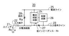
図1は、本発明の第1の参考形態として、スイッチの接点腐食防止装置20の概略的な電気的構成を示す。本参考形態の構成は、図20に示す先行技術の構成とほぼ対応している。すなわち、スイッチ21は、入力端子22と接地との間に接続される接点を有し、接点の定格電流容量は、たとえば最大で数A程度である。入力端子22に与えられる電圧は、入力信号ライン23を介してECUなどに入力される。スイッチ21の接点が閉じているときには、たとえば200mAに近い大電流が、電流供給回路24を介して、入力端子22からスイッチ21の接点に、電源ライン25からパルス的に供給される。この大電流経路を流れる電流値は、接点の酸化膜を除去しうる電流として、接点の定格電流容量に応じて設定される。
【0040】
電流供給回路24は、制御回路26から出力される制御信号によって駆動される。制御回路26は、入力信号ライン23の電圧を検出し、スイッチ21の接点が開状態であるときに対応する電圧であれば、電流供給回路24からスイッチ21の接点に電流を供給可能な低インピーダンス状態にする制御を行う。なお、制御回路26の入力および入力信号ライン23と入力端子22との間には、入力側に大電流などが流れ込むのを防ぐ保護抵抗27が接続される。また、スイッチ21の接点の開閉状態を入力する際の入力インピーダンスを決定する入力抵抗28が入力端子22と電源ライン25との間に接続されている。入力抵抗28の抵抗値をRaとし、電流供給回路24のインピーダンスをRbとし、スイッチ21の接点の閉状態での抵抗値をRcとすると、Ra≫Rb≫Rcである。
【0041】
本参考形態では、スイッチ21の接点の開閉状態に応じた電気的な入力を行う際に、接点に定格電流容量に対応する腐食防止用の電流を流すために、電流供給回路24を設けている。電流供給回路24は、接点に電流を供給するか否かを制御可能であり、電流供給時には、接点の開閉状態入力用の入力インピーダンスRaよりも低いインピーダンスRbとなり、接点が閉状態であれば、接点に腐食防止用の電流を供給することが可能な電流供給手段とし機能する。
【0042】
電流供給回路24は、制御回路26によって制御される。制御回路26は、スイッチ21の接点の開閉状態を検知して、接点が開状態のとき、および閉状態中に予め定められる保持時間には、電流供給回路24から接点への電流供給を行い、接点が閉状態で該保持時間外では、電流供給回路24から接点への電流供給を遮断するように制御する制御手段として機能する。このような電流供給回路24は、定電流回路とスイッチ回路との組合わせや、図20に示すような低抵抗14とスイッチングトランジスタ11との直列回路など、種々の構成で実現することができる。また、電流供給回路24は低損失化されるので、制御回路26や入力抵抗28などを含めて、本実施形態のスイッチの接点腐食防止装置20は、半導体集積回路として容易にIC化することができる。
【0043】
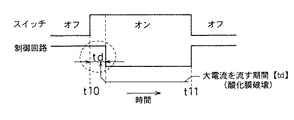
図2は、スイッチ21の開閉操作と、制御回路26による電流供給回路24の制御状態とを示す。本実施形態では、基本的にスイッチ21の接点が開状態のオフ時に、電流供給回路24は電流供給が可能な状態となるように、制御回路26によって制御される。ただし、スイッチ21の接点は開状態であるので、接点には大電流は流れず、消費電力等が増大することはない。スイッチ21が時刻t10でオフからオンになると、制御回路26は、電流供給回路24の電流供給状態を、さらに保持時間tdの期間だけ継続する。この保持時間tdの期間には、スイッチ21の接点が閉状態になるので、接点に大電流が流れる。電流供給回路24のインピーダンスRbを、接点に酸化膜破壊用に充分な電流を流すように設定しておけば、保持時間tdの間に、腐食防止を図ることができる。保持時間tdが経過すると、時刻t11まで、接点が閉状態の間は、電流供給回路24が電流供給を停止するように、制御回路26によって制御される。時刻t11でスイッチ21の接点がオンからオフに遷移すれば、制御回路26は電流供給回路24を制御して、電流供給状態に戻す。なお、保持時間tdは、時刻t10から時刻t11までの間に設ければよい。
【0044】
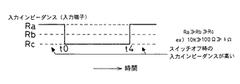
図3は、図2に示すような制御状態に対応する入力端子22から見た入力インピーダンスの変化を示す。時刻t10でスイッチ21の接点が閉状態になる前、および時刻t11以降は、スイッチ21の接点は開状態であり、入力インピーダンスは、電流供給回路24のインピーダンスRbとほぼ等しくなる。時刻t10保持時間tdの間は、スイッチ21の接点の閉状態での抵抗値Rcと電流供給回路24のインピーダンスRbとが並列に接続されていると考えることができ、並列のインピーダンスは、Rb≫Rcであるので、Rcと見なすことができる。保持時間tdが過ぎてから、時刻t11に達するまでの接点の閉状態の期間では、電流供給回路24からの電流供給が停止し、入力インピーダンスは、スイッチ21の接点の閉状態での抵抗値Rcと入力抵抗28の抵抗値Raとの並列状態での合成抵抗値となる。ただし、Ra≫Rb≫Rcであるので、合成抵抗値はRcと見なすことができる。時刻t11以降は、電流供給回路24が電流供給状態となり、そのインピーダンスRbが入力インピーダンスとなる。
【0045】
以上のように、本参考形態では、スイッチ21の接点の開閉状態に応じた電気的な入力を行う際に、接点に通電容量に対応する腐食防止用の電流を流すために、電流供給回路24と制御回路26とを設ける。電流供給回路24は、スイッチ21の接点に電流を供給するか否かを制御可能であり、電流供給時には、接点の開閉状態入力用の入力インピーダンスRaよりも低いインピーダンスRbとなり、接点が閉状態であれば、接点に腐食防止用の電流を供給することが可能である。制御回路26は、接点の開閉状態を検知して、時刻t10以前および時刻t11以降で接点が開状態のとき、および時刻t10から時刻t11までの閉状態中に予め定められる保持時間tdには、電流供給回路24から接点への電流供給を行い、接点が時刻t10から時刻t11までの閉状態で、保持時間td外では、電流供給回路24から接点への電流供給を遮断するように制御する。
【0046】
接点が開状態のときには、電流供給回路24は接点の開閉状態入力用の入力インピーダンスRaよりも低いインピーダンスRbとなるけれども、スイッチ21の接点は開状態であるので、大電流は流れず、消費電力の増加や発熱の増加を招くことはない。接点の開状態でも入力端子22の入力インピーダンスが低いので、耐ノイズ性などを向上させ、開閉状態を検出する信頼性を高めることができる。スイッチ21の接点が閉状態となれば、保持時間tdだけ電流供給回路24から接点に腐食防止用の電流が供給され、消費電力や発熱の増大を避けながら、接点の酸化膜を除去して腐食防止を有効に図ることができる。
【0047】
また本参考形態では、制御回路26が保持時間tdを、スイッチ21の接点が開状態から閉状態に遷移した時刻t10後に継続して設定している。スイッチ21の接点が開状態のときから連続して、時刻t10で接点が開状態から閉状態に遷移した後で保持時間tdが経過するまで、電流供給回路24から低インピーダンス状態で接点に電流を供給すればよいので、制御回路26による電流供給回路24の制御を簡易化することができる。
【0048】
図4は、本発明の第2の参考形態として、図1に示す構成を用いて行うスイッチ21の開閉操作と、制御回路26による電流供給回路24の制御状態とを示す。本参考形態で、制御回路26は、電流供給回路24からの電流供給を、時刻t20でスイッチ21の接点が開状態から閉状態に遷移した後で第1の保持時間tdだけ継続した後、さらに電流供給回路24からの電流供給を定期的に繰返す。すなわち、時刻t21や時刻t22で電流供給を第2の保持時間teだけそれぞれ行い、時刻t23でスイッチ21の接点が閉状態から開状態に遷移すると、電流供給状態に戻る。スイッチ21の接点の閉状態が長時間継続するときには、第2の保持時間teが繰返して設定され、腐食防止用の電流によって酸化膜の生成を防ぐことができる。
【0049】
図5は、本発明の第3の参考形態として、図1に示す構成を用いて行うスイッチ21の開閉操作と、制御回路26による電流供給回路24の制御状態とを示す。本参考形態で、制御回路26は、電流供給回路24からの電流供給を、時刻t30でスイッチ21の接点が開状態から閉状態に遷移した直後は一旦停止し、前述の保持時間tdをこの一旦停止した後に設定する。時刻t30でスイッチ21の接点を開状態から閉状態に遷移させる際に、一旦電流供給回路24から接点への電流供給を停止するので、接点の開閉状態が切換えられる際の突入電流によって、接点が溶着することを防止することができる。
【0050】
図6は、本発明の第4の参考形態として、図1に示す構成を用いて行うスイッチ21の開閉操作と、電流供給回路24から接点に供給される負荷電流の変化とを示す。本参考形態で、電流供給回路24からの電流供給は、急激な電流変化を抑えて行われる。図6(a)は、電流供給回路24から流れ出す電流量をリニアに増減させる状態を示す。積分回路などを利用すれば、このようなリニアな変化を生じさせることができる。図6(b)は、電流供給回路24から流れ出す電流量を段階的に増減させる状態を示す。これらの電流変化は、電流供給回路24がスイッチ21の接点への電流供給の状態を変化させる際に、インピーダンスの変化を緩慢化して行うことによって実現される。電流供給回路24からスイッチ21の接点に供給される電流は、電流供給回路24のインピーダンスの変化が緩慢化されているので、急激に変化することがなく、ノイズ発生を抑制することができる。また、接点が開閉する際に火花などが発生しにくくなり、接点の溶着なども生じにくくすることができる。
【0051】
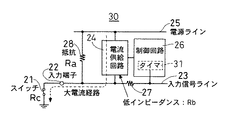
図7は、本発明の実施の第1形態として、スイッチの接点腐食防止装置30の概略的な電気的構成を示す。本実施形態では、タイマ31が、スイッチ21の接点の開閉周期を監視し、制御回路26はその開閉周期を次の保持時間tdに反映させて、保持時間tdの長さを調整する。図8および図9は、スイッチ21の接点の開閉状態と、制御回路26による制御で電流供給回路24から供給される電流の変化とを示す。タイマ31は、保持時間tdが設定されるので、設定されている保持時間tdを認識して、スイッチ21の接点の開閉についての時間的な情報を収集する開閉時間情報収集手段としても機能する。すなわち、タイマ31は接点の開閉周期を監視し、制御回路26はその開閉周期に応じて、保持時間tdの長さを変更する。本実施形態のスイッチの接点腐食防止装置30も容易にIC化することができる。
【0052】
図8では、スイッチ21がオンになる周期が長いので、オフからオンに遷移した時点で保持時間td2が設定される頻度が小さくなる。このために、保持時間td2を長くし、腐食防止が充分に行われるようにする。図9では、スイッチ21がオンになる周期が短いので、オフからオンに遷移した時点で保持時間td3が設定される頻度が大きくなる。このために、保持時間td3を短くして、電流供給回路24の低損失化を図る。本実施形態では、タイマ31に設定されるスイッチ21の接点の開閉についての時間的な情報を収集して、電流供給回路24から接点に腐食防止用の電流を流す保持時間td2、td3の長さを変更する。接点の開閉周期が長くなると保持時間td2も長くして腐食防止を確実に図り、接点の開閉周期が短くなると保持時間td3も短くすることによって、省エネルギや発熱低減を図り、しかも腐食防止も確実に行うことができる。
【0053】
図10は、本発明の実施の第2形態として、スイッチの接点腐食防止装置40の概略的な電気的構成を示す。本実施形態では、電流供給回路24の温度を検出する温度検出部41を設ける。制御回路26は、温度検出部41が検出する温度が高くなると、保持時間td,td2,td3,teが短くなるように制御する。温度検出部41によって検出する電流供給回路24の温度が、電流供給回路24の電流供給による自己発熱などで高温になると、スイッチ21の接点に腐食防止用の電流を供給する保持時間td,td2,td3,teを短くして、電流供給回路24の自己発熱を抑制し、熱損失による素子破壊などからの保護を図ることができる。本実施形態のスイッチの接点腐食防止装置40も容易にIC化することができる。
【0054】
図11は、本発明の第5の参考形態として、スイッチの接点腐食防止装置50の概略的な電気的構成を示す。本参考形態の制御回路26は、アナログ/デジタル変換を行うA/D回路51によって、入力信号ライン23の電圧値を検出し、スイッチ21の接点の腐食状態を判定する。A/D回路51は、スイッチ21の接点が閉状態となるときの接点のインピーダンスを検出するインピーダンス検出手段として機能する。接点の腐食が進行すればインピーダンスが上昇し、接点に生じる電圧も高くなる。制御回路26は、A/D回路51によって検出される接点の閉状態のインピーダンスの高低に応じて、保持時間td等を長短に変更するように制御する。スイッチ21の接点について、酸化が進行すると、閉状態でのインピーダンスが高くなるので、電流供給回路24から腐食防止用の電流を供給する保持時間td等を長くして、酸化膜の確実な除去を図ることができる。本実施形態のスイッチの接点腐食防止装置50も容易にIC化することができる。
【0055】
図12は、本発明の第6の参考形態として、スイッチの接点腐食防止装置60の概略的な電気的構成を示す。本実施形態の制御回路26は、外部のマイコン61やECU、プログラムコントローラなどから、たとえば自動車各種制御に用いる使用環境などについての情報を収集する。すなわち、マイコン61などは、スイッチ21の使用環境に関する情報を収集する使用環境情報収集手段として機能する。制御回路26は、マイコン61などによって収集される使用環境に応じて、保持時間td等を設定する頻度を変更する。たとえば周囲温度などの情報や、自動車でのエンジン始動時などに関する情報などを収集し、使用環境に適合して、酸化膜除去用の腐食防止電流を流す保持時間td等を変更し、スイッチ21の接点の腐食防止を有効に図ることができる。本参考形態のスイッチの接点腐食防止装置60も容易にIC化することができる。
【0056】
図13は、本発明の第7の参考形態として、各形態で示す構成を用いて行うスイッチ21の開閉操作と、制御回路26の制御による電流供給回路24のインピーダンス変化とを示す。本実施形態で、電流供給回路24からの電流供給は、時刻t40でスイッチ21がオフからオンになるときに保持時間td1で継続し、時刻t41でスイッチ21オンからオフになるときは、遅延時間td4だけ遅れて電流供給状態に変化する。機械的な接点で形成されるスイッチ21では、オンとオフとの開閉状態の変化の際にチャタリングが生じる。制御回路26は、接点が閉状態から開状態に遷移しても、接点のチャタリングが収束する時間を含めて予め設定される遅延時間td4が経過するまでは、電流供給回路24の電流供給状態への移行を遅延させる。スイッチ21の接点が閉状態から開状態に遷移する際にチャタリングが生じて、接点が短時間の繰返しで閉状態になっても、電流供給回路24が電流供給状態に移行するのは予め設定される遅延時間td4が過ぎてからであるので、チャタリングによる瞬間的な大電流の流出を防止することができる。
【0057】
図14は、本発明の第8の参考形態として、スイッチの接点腐食防止装置70の概略的な電気的構成を示す。本参考形態には、抵抗71およびコンデンサ72と、切換えスイッチ73とを含む電流供給回路74は、制御回路76によって切換えスイッチ73が制御される。切換えスイッチ73は、機械的な接点を有するリレーなどを使用したり、電子的なスイッチング素子を用いて構成することができる。本実施形態のスイッチの接点腐食防止装置70も、コンデンサ72を除いて容易にIC化することができる。コンデンサ72の容量を数100pF以上に大きくする場合は、コンデンサ72を外付けとしてIC化することができる。
【0058】
電流供給回路74では、スイッチ21の接点の開閉状態に応じた電気的な入力を行う際に、接点に定格電流容量に対応する腐食防止用の電流を流すために、電流を供給するか否かを切換えスイッチ73で制御可能である。電流供給を行わないときには、コンデンサ72に電源ライン25から抵抗71を介して電荷を蓄える充電を行い、電流供給時にはコンデンサ72に蓄えられた電荷を放電する。スイッチ21の接点が閉状態であれば、切換えスイッチ73を充電側から放電側に切換えることによって、接点に腐食防止用の電流を供給することが可能となる。切換えスイッチ73の切換えは、制御回路76によって制御される。制御回路76は、スイッチ21の接点の開閉状態を検知して、接点が閉状態のときに、電荷が充電されていれば、電流供給手段74から接点への電流供給を行うように制御する。
【0059】
図15は、図14のスイッチ21のオン・オフ操作と、接点に流れる負荷電流の変化とを示す。制御回路76は、スイッチ21の接点の開閉状態を検知して、接点が閉状態のときに、コンデンサ72に電荷が充電されていれば、コンデンサ72に蓄えられた電荷を放電して、電流供給回路74から接点への電流供給を行うように制御する。接点が開状態のときには、電流供給回路74のコンデンサ72は電荷を蓄える充電を行う。スイッチ21の接点が閉状態となって、コンデンサ72に充分な電荷が蓄えられていれば、蓄えられた電荷を放電して、接点に腐食防止用の電流を供給する。電流供給回路74からスイッチ21の接点に、腐食防止用の電流を間欠的に供給するので、消費電力や発熱の増大を避けながら、接点の酸化膜を除去して腐食防止を有効に図ることができる。
【0060】
図16は、本発明の第9の参考形態として、スイッチの接点腐食防止装置80の概略的な電気的構成を示す。本参考形態では、電流供給回路24に電源ライン25Aから、スイッチ21の開閉状態の入力のためなど、他の回路部分に電源ライン25Bから印加する電圧よりも高い電圧を印加する。たとえば自動車にスイッチの接点腐食防止装置80を含むECUなどを搭載する場合、電源ライン25Aには、発電機やバッテリから直接供給される+Bラインからの電圧を与える。電源ライン25Bには、ロジック回路用に安定化された電圧を与える。
【0061】
図17および図18は、本参考形態で、制御回路26が電流供給回路24を制御して、図3および図4に示すように保持時間td,teを設定するときのスイッチ21操作のオン・オフ操作と、接点に流れる負荷電流の変化とをそれぞれ示す。各保持時間td,teでは接点に高電圧が印加されるので、酸化膜などが形成されていても、その破壊をしうる大電流を容易に流すことができる。
【0067】
【発明の効果】
以上のように本発明によれば、スイッチの接点の開閉に周期に応じて、たとえば接点の開閉周期が短くなると保持時間も短くして、省エネルギや発熱低減を図り、しかも腐食防止も確実に行うことができる。
【0068】
また本発明によれば、電流供給手段が電流供給による自己発熱で高温になると、スイッチの接点に腐食防止用の電流を供給する保持時間を短くして、熱損失による素子破壊などからの保護を図ることができる。
【図面の簡単な説明】
【図1】本発明の第1の参考形態として、スイッチの接点腐食防止装置20の概略的な電気的構成を示すブロック図である。
【図2】図1の参考形態で、スイッチ21の開閉操作と、制御回路26による電流供給回路24の制御状態とを示すタイムチャートである。
【図3】図2に示すような制御状態に対応して、入力端子22から見た入力インピーダンスの変化を示すタイムチャートである。
【図4】本発明の第2の参考形態として、図1に示す構成を用いて行うスイッチ21の開閉操作と、制御回路26による電流供給回路24の制御状態とを示すタイムチャートである。
【図5】本発明の第3の参考形態として、図1に示す構成を用いて行うスイッチ21の開閉操作と、制御回路26による電流供給回路24の制御状態とを示すタイムチャートである。
【図6】本発明の第4の参考形態として、図1に示す構成を用いて行うスイッチ21の開閉操作と、電流供給回路24から接点に供給される負荷電流の変化とを示すタイムチャートである。
【図7】本発明の実施の第1形態として、スイッチの接点腐食防止装置30の概略的な電気的構成を示すブロック図である。
【図8】図7の実施形態で、スイッチ21の接点の開閉状態と、制御回路26による制御で電流供給回路26から供給される電流の変化とを示すタイムチャートである。
【図9】図7の実施形態で、スイッチ21の接点の開閉状態と、制御回路26による制御で電流供給回路26から供給される電流の変化とを示すタイムチャートである。
【図10】本発明の実施の第2形態として、スイッチの接点腐食防止装置40の概略的な電気的構成を示すブロック図である。
【図11】本発明の第5の参考形態として、スイッチの接点腐食防止装置50の概略的な電気的構成を示すブロック図である。
【図12】本発明の第6の参考形態として、スイッチの接点腐食防止装置60の概略的な電気的構成を示すブロック図である。
【図13】本発明の第7の参考形態として、各形態で示す構成を用いて行うスイッチ21の開閉操作と、制御回路26の制御による電流供給回路24のインピーダンス変化とを示すタイムチャートである。
【図14】本発明の第8の参考形態として、スイッチの接点腐食防止装置70の概略的な電気的構成を示すブロック図である。
【図15】図14の参考形態で、スイッチ21のオン・オフ操作と、接点に流れる負荷電流の変化とを示すタイムチャートである。
【図16】本発明の第9の参考形態として、スイッチの接点腐食防止装置80の概略的な電気的構成を示すブロック図である。
【図17】図16の参考形態でのスイッチ21操作のオン・オフ操作と、接点に流れる負荷電流の変化とをそれぞれ示すタイムチャートである。
【図18】図16の参考形態でのスイッチ21操作のオン・オフ操作と、接点に流れる負荷電流の変化とをそれぞれ示すタイムチャートである。
【図19】従来から、大電流用スイッチを使用して、電子制御の入力信号を得るために用いられている基本的な回路構成を示すブロック図である。
【図20】先行技術の基本的な電気的構成を示すブロック図である。
【図21】図20の先行技術で、スイッチ1の接点の開閉状態と、制御回路12によるスイッチングトランジスタ11の制御状態を示すタイムチャートである。
【図22】図21のようにスイッチ1を開閉させる操作を行うときに、入力端子2から見た入力インピーダンスを示すタイムチャートである。
【符号の説明】
20,30,40,50,60,70,80 スイッチの接点腐食防止装置
21 スイッチ
22 入力端子
23 入力信号ライン
24,74 電流供給回路
25,25A,25B 電源ライン
26,76 制御回路
31 タイマ
41 温度検出部
51 A/D回路
61 マイコン[0001]
TECHNICAL FIELD OF THE INVENTION
The present invention relates to a switch corrosion protection device for preventing corrosion by breaking an oxide film formed on a contact when a large current switch is used as an input for electronic control.
[0002]
[Prior art]
2. Description of the Related Art Conventionally, inputs for various electronic controls are often performed using contact points of switches. For example, in order to perform various controls in an automobile, switch contacts that mechanically open and close together with various sensors are used in order to provide input signals for control to many electronic control units (ECUs). In automobiles and the like, there are many vibrations and shocks, and the switches are required to have mechanical durability. In addition, when the distance to the ECU or the like is long, a certain large current, for example, about several tens mA to several A, is intermittently input. Therefore, a switch with a relatively large current capacity and a large current specification is used. In an input signal of an ECU or the like, a relatively small current value, for example, a change of about several hundred μA to several mA can be detected. However, noise increases in control of an automobile or the like. This is because it is necessary to increase the change in the current value.
[0003]
FIG. 19 shows a basic circuit configuration conventionally used to obtain an electronic control input signal using a large current switch. The
[0004]
The contact of the mechanical switch is usually made of copper (Cu) and further plated with tin (Sn). However, when tin plating is applied, the electrical conductivity is slightly deteriorated. Therefore, gold (Au) plating, which has higher electrical conductivity than tin plating, is used for the contact of a switch through which a large current flows.
[0005]
However, gold plating has the disadvantage that the coating is softer than tin plating, and the contacts are easily rusted due to abrasion at the time of contacting the contacts. The film is destroyed to prevent corrosion.
[0006]
FIG. 20 shows a basic electrical configuration of the prior art of the switch
[0007]
In the prior art shown in FIG. 20, the low resistance 4 is connected in series between the collector and the emitter of an NPN type switching transistor (Tr) 11. The base of the switching transistor is driven by a control signal output from the
[0008]
FIG. 21 shows the open / closed state of the contact of the
[0009]
FIG. 22 shows the input impedance viewed from the input terminal 2 when the operation of opening and closing the
[0010]
A prior art in which a pulse current is applied to detect on / off of a switch contact including a relay and the like and the effect of contact failure due to generation of an oxide film of the contact is reduced is also disclosed in Japanese Patent Application Laid-Open No. 7-14463. . In this prior art, an electric charge charged in a capacitor via a resistor is supplied to a contact as a pulse current by making a switching transistor conductive with an output from an oscillator. However, in FIG. 1, the collector of a
[0011]
[Problems to be solved by the invention]
According to the basic concept of the prior art disclosed in JP-A-6-96637 and JP-A-7-14463, when a switch contact is in a closed state, a large current is applied in a pulsed manner to cause corrosion due to oxide film formation. Can be prevented, and power consumption and heat generation can be reduced. However, in these prior arts, the switching element is turned on only when the contact of the switch is in the closed state, and the input impedance of the input signal line for detecting the open / closed state of the contact is reduced. When the contacts of the switch are open, the input impedance increases, the EMI (Electro Magnetic Interference) level indicating noise resistance deteriorates, and the input level fluctuates with respect to leak current. Occurs. EMI is generally a functional disturbance that an electronic device experiences from the electromagnetic environment. In the case of an electronic device mounted on an automobile, EMI sources are roughly classified into two types: noise of the own vehicle such as electric noise generated when a switch system is turned ON / OFF, and external noise such as broadcast radio waves.
[0012]
Further, in the prior art of Japanese Patent Application Laid-Open No. 7-14463, the electric charge stored in the capacitor 53 flows as a pulse current Ip at the oscillation cycle of the oscillator 52 irrespective of the open / close state of the contact 2. For this reason, if an attempt is made to reduce the frequency of occurrence of the pulse current Ip to save power, even when the contact 2 is turned on, a current for preventing corrosion does not always flow.
[0013]
SUMMARY OF THE INVENTION An object of the present invention is to provide a switch contact corrosion prevention device capable of reliably preventing corrosion and improving the reliability of detecting the open / closed state of a switch contact.
[0014]
[Means for Solving the Problems]
The present invention is a low-impedance means capable of setting an input impedance of an input signal line for determining an open / closed state of a contact of a switch to a low-impedance state capable of flowing a corrosion prevention current to a contact of the closed switch,
In a switch corrosion prevention device comprising: a high-impedance state in which the input impedance of the input signal line is higher than the low-impedance state;
The low impedance means keeps the input impedance of the input signal line in the low impedance state while the contact of the switch is open, and sets the input impedance of the input signal line to a predetermined holding time while the contact of the switch is closed. A corrosion prevention current is supplied to the switch in the low impedance state, and the length of the holding time is changed according to a switching cycle of the contact.
[0025]
According to the present invention, the holding time in which the input impedance of the input signal line is set to the low impedance state by the low impedance means and the current for corrosion prevention flows while the switch contact is closed according to the switching cycle of the switch contact Since the length of the contact is changed, for example, when the opening / closing cycle of the contact is shortened, the holding time is also shortened, so that energy saving and heat generation can be reduced, and corrosion can be reliably prevented.
[0026]
Further, the present invention is connected to an input signal line for judging an open / closed state of a contact of a switch, and the input impedance of the input signal line is a low impedance capable of flowing a corrosion prevention current to a contact of the switch in a closed state. Low impedance means that can be in a state;
And a high impedance means connected to the input signal line and having a higher impedance than the impedance of the low impedance means.
The low impedance means is a current supply means for supplying a corrosion prevention current to a contact of the switch,
Including temperature detection means for detecting the temperature of the current supply means,
While the switch contact is open, the input impedance of the input signal line is maintained in a low impedance state by the low impedance means, and for a predetermined holding time while the switch contact is closed, the input impedance of the input signal line is maintained. Is set to a low impedance state by the low impedance means, the corrosion prevention current flows, and based on the temperature of the current supply means detected by the temperature detection means, the higher the temperature, the shorter the holding time. This is a contact corrosion prevention device.
[0027]
According to the present invention, the temperature of the current supply unit is detected by the temperature detection unit. When the current supply means self-heats due to the current supply and becomes high temperature, the holding time for supplying the current for preventing corrosion to the switch contacts is shortened, the self-heating of the current supply means is suppressed, and the element is damaged due to heat loss. Can be protected.
[0038]
BEST MODE FOR CARRYING OUT THE INVENTION
Hereinafter, embodiments and reference embodiments of the present invention will be described with reference to FIGS. Corresponding parts in each embodiment have the same reference characters allotted, and overlapping description will be omitted. Also, a plurality of embodiments described below can be used in combination.
[0039]
FIG. 1 shows a schematic electrical configuration of a switch contact
[0040]
The
[0041]
In the present embodiment, the
[0042]
The
[0043]
FIG. 2 shows an opening and closing operation of the
[0044]
FIG. 3 shows a change in the input impedance viewed from the
[0045]
As described above, in the present embodiment, when an electrical input is performed in accordance with the open / closed state of the contact of the
[0046]
When the contact is in the open state, the
[0047]
Further, in the present embodiment, the
[0048]
FIG. 4 shows an opening / closing operation of the
[0049]
FIG. 5 shows an opening / closing operation of the
[0050]
FIG. 6 shows an opening / closing operation of the
[0051]
FIG. 7 shows a schematic electrical configuration of a switch contact
[0052]
In FIG. 8, since the cycle at which the
[0053]
FIG. 10 shows a schematic electrical configuration of a switch contact
[0054]
FIG. 11 shows a schematic electrical configuration of a switch contact
[0055]
FIG. 12 shows a schematic electrical configuration of a switch contact
[0056]
FIG. 13 shows, as a seventh reference embodiment of the present invention, an opening / closing operation of the
[0057]
FIG. 14 shows a schematic electrical configuration of a switch contact
[0058]
In the
[0059]
FIG. 15 shows the on / off operation of the
[0060]
FIG. 16 shows a schematic electrical configuration of a switch contact
[0061]
FIGS. 17 and 18 show the present embodiment, in which the
[0067]
【The invention's effect】
As described above, according to the present invention, according to the cycle of opening and closing the contacts of the switch, for example, when the opening and closing cycle of the contacts is shortened, the holding time is also shortened, thereby saving energy and reducing heat generation, and also reliably preventing corrosion. It can be carried out.
[0068]
Further, according to the present invention, when the current supply means is heated by self-heating due to the current supply and becomes high temperature, the holding time for supplying the current for preventing corrosion to the contact of the switch is shortened to protect the device from element destruction due to heat loss. Can be planned.
[Brief description of the drawings]
FIG. 1 is a block diagram showing a schematic electrical configuration of a switch contact
FIG. 2 is a time chart showing an opening and closing operation of a
FIG. 3 is a time chart showing a change in input impedance as viewed from an
4 is a time chart showing, as a second reference embodiment of the present invention, an opening / closing operation of a
FIG. 5 is a time chart showing an opening / closing operation of a
FIG. 6 is a time chart showing an opening / closing operation of a
FIG. 7 is a block diagram showing a schematic electrical configuration of a switch contact
8 is a time chart showing an open / close state of a contact point of a
9 is a time chart showing an open / closed state of a contact point of a
FIG. 10 is a block diagram showing a schematic electrical configuration of a switch contact
FIG. 11 is a block diagram showing a schematic electrical configuration of a switch contact
FIG. 12 is a block diagram showing a schematic electrical configuration of a switch contact
FIG. 13 is a time chart showing, as a seventh reference embodiment of the present invention, an opening / closing operation of the
FIG. 14 is a block diagram showing a schematic electrical configuration of a switch contact
FIG. 15 is a time chart showing the on / off operation of the
FIG. 16 is a block diagram showing a schematic electrical configuration of a switch contact
17 is a time chart showing the on / off operation of the
18 is a time chart showing the on / off operation of the
FIG. 19 is a block diagram showing a basic circuit configuration conventionally used to obtain an electronic control input signal using a large current switch.
FIG. 20 is a block diagram showing a basic electrical configuration of the prior art.
21 is a time chart showing the open / close state of the contact of the
FIG. 22 is a time chart showing the input impedance as viewed from the input terminal 2 when performing the operation of opening and closing the
[Explanation of symbols]
20, 30, 40, 50, 60, 70, 80 Contact corrosion prevention device for switch
21 switch
22 input terminal
23 Input signal line
24,74 current supply circuit
25, 25A, 25B power supply line
26,76 control circuit
31 timer
41 Temperature detector
51 A / D circuit
61 microcomputer
Claims (2)
該入力信号ラインの入力インピーダンスが該低インピーダンス状態よりも高い高インピーダンス状態で、接点の開閉状態を判定可能な高インピーダンス手段とを備えるスイッチの腐食防止装置において、
低インピーダンス手段は、スイッチの接点が開状態の間、入力信号ラインの入力インピーダンスを該低インピーダンス状態に保ち、スイッチの接点が閉状態中に予め定められる保持時間には、入力信号ラインの入力インピーダンスを該低インピーダンス状態にして腐食防止電流を流すとともに、接点の開閉周期に応じて、該保持時間の長さを変更することを特徴とするスイッチの接点腐食防止装置。Low impedance means for setting an input impedance of an input signal line for determining an open / closed state of a switch contact to a low impedance state capable of flowing a corrosion prevention current to a closed switch contact;
In a switch corrosion prevention device comprising: a high-impedance state in which the input impedance of the input signal line is higher than the low-impedance state;
The low impedance means keeps the input impedance of the input signal line in the low impedance state while the contact of the switch is open, and sets the input impedance of the input signal line to a predetermined holding time while the contact of the switch is closed. A corrosion prevention current is supplied to the switch in the low impedance state, and the length of the holding time is changed according to a switching cycle of the contact.
該入力信号ラインの入力インピーダンスが該低インピーダンス状態よりも高い高インピーダンス状態で、接点の開閉状態を判定可能な高インピーダンス手段とを備えるスイッチの腐食防止装置において、
スイッチの接点に腐食防止電流を供給する電流供給手段と、
電流供給手段の温度を検出する温度検出手段とを含み、
低インピーダンス手段は、スイッチの接点が開状態の間、入力信号ラインの入力インピーダンスを該低インピーダンス状態に保ち、スイッチの接点が閉状態中に予め定められる保持時間には、入力信号ラインの入力インピーダンスを該低インピーダンス状態にして腐食防止電流を流すとともに、温度検出手段が検出する電流供給手段の温度に基づき、温度が高くなると該保持時間を短くすることを特徴とするスイッチの接点腐食防止装置。Low impedance means for setting an input impedance of an input signal line for determining an open / closed state of a switch contact to a low impedance state capable of flowing a corrosion prevention current to a closed switch contact;
In a switch corrosion prevention device comprising: a high-impedance state in which the input impedance of the input signal line is higher than the low-impedance state;
Current supply means for supplying a corrosion prevention current to a switch contact;
Temperature detection means for detecting the temperature of the current supply means,
The low impedance means keeps the input impedance of the input signal line in the low impedance state while the contact of the switch is open, and sets the input impedance of the input signal line to a predetermined holding time while the contact of the switch is closed. A corrosion prevention current flowing in the low-impedance state, and the holding time is shortened when the temperature rises based on the temperature of the current supply means detected by the temperature detection means.
Priority Applications (1)
| Application Number | Priority Date | Filing Date | Title |
|---|---|---|---|
| JP2001150927A JP3587802B2 (en) | 2001-05-21 | 2001-05-21 | Switch contact corrosion prevention device |
Applications Claiming Priority (1)
| Application Number | Priority Date | Filing Date | Title |
|---|---|---|---|
| JP2001150927A JP3587802B2 (en) | 2001-05-21 | 2001-05-21 | Switch contact corrosion prevention device |
Publications (3)
| Publication Number | Publication Date |
|---|---|
| JP2002343171A JP2002343171A (en) | 2002-11-29 |
| JP3587802B2 true JP3587802B2 (en) | 2004-11-10 |
| JP2002343171A5 JP2002343171A5 (en) | 2005-02-03 |
Family
ID=18995867
Family Applications (1)
| Application Number | Title | Priority Date | Filing Date |
|---|---|---|---|
| JP2001150927A Expired - Fee Related JP3587802B2 (en) | 2001-05-21 | 2001-05-21 | Switch contact corrosion prevention device |
Country Status (1)
| Country | Link |
|---|---|
| JP (1) | JP3587802B2 (en) |
Cited By (1)
| Publication number | Priority date | Publication date | Assignee | Title |
|---|---|---|---|---|
| US11636988B2 (en) | 2020-12-24 | 2023-04-25 | Kubota Corporation | Electronic control device, work vehicle, and input circuit |
Families Citing this family (16)
| Publication number | Priority date | Publication date | Assignee | Title |
|---|---|---|---|---|
| JP3625473B1 (en) | 2004-04-05 | 2005-03-02 | 富士通テン株式会社 | Contact corrosion prevention method and apparatus |
| JP3625474B1 (en) | 2004-04-05 | 2005-03-02 | 富士通テン株式会社 | Contact corrosion prevention circuit |
| JP3625472B1 (en) | 2004-04-05 | 2005-03-02 | 富士通テン株式会社 | Contact corrosion prevention device |
| JP2006310287A (en) * | 2005-03-30 | 2006-11-09 | Fujitsu Ten Ltd | Corrosion prevention method, corrosion prevention device, signal processor, and control unit |
| CN100561624C (en) | 2005-03-30 | 2009-11-18 | 富士通天株式会社 | Prevent corrosion device |
| JP4451855B2 (en) * | 2006-03-30 | 2010-04-14 | 富士通テン株式会社 | Signal processing apparatus and control unit |
| FR2899373B1 (en) * | 2006-04-04 | 2013-03-15 | Airbus France | DEVICE FOR DETECTING THE STATUS OF A SWITCH |
| JP4495124B2 (en) * | 2006-08-31 | 2010-06-30 | 富士通テン株式会社 | Signal processing device, vehicle control unit including signal processing device, and vehicle including vehicle control unit |
| JP5076415B2 (en) * | 2006-09-14 | 2012-11-21 | 日本精工株式会社 | Electric power steering control device |
| JP2008298524A (en) * | 2007-05-30 | 2008-12-11 | Denso Corp | Circuit testing device and its operation method |
| JP5163723B2 (en) * | 2010-09-24 | 2013-03-13 | 株式会社デンソー | Switch monitoring device, control device, and control method |
| JP6153061B2 (en) * | 2013-05-10 | 2017-06-28 | 日本精機株式会社 | Shift position display device |
| JP6218714B2 (en) * | 2014-09-26 | 2017-10-25 | 三菱電機株式会社 | Protective relay device |
| JP6851284B2 (en) * | 2017-08-01 | 2021-03-31 | 株式会社Jvcケンウッド | Electronics |
| CN113923555B (en) * | 2021-10-13 | 2024-02-06 | 维沃移动通信有限公司 | Charging control circuit and charging control method for earphone |
| KR102644289B1 (en) * | 2023-09-18 | 2024-03-06 | 인터콘시스템스 주식회사 | Digital signal input circuit for train |
Family Cites Families (11)
| Publication number | Priority date | Publication date | Assignee | Title |
|---|---|---|---|---|
| JPS54122069U (en) * | 1978-02-16 | 1979-08-27 | ||
| JPS63237319A (en) * | 1987-03-26 | 1988-10-03 | 株式会社 三ツ葉電機製作所 | Reliability securing apparatus for switch contact for motor control |
| JPH01281621A (en) * | 1988-05-09 | 1989-11-13 | Nippon Denso Co Ltd | Current supply circuit for vehicle switch |
| JPH02278620A (en) * | 1989-04-19 | 1990-11-14 | Oki Electric Ind Co Ltd | No-voltage contact input system |
| JPH03205710A (en) * | 1989-12-29 | 1991-09-09 | Sumitomo Electric Ind Ltd | Contact purifying circuit for power supply control electromagnetic relay of antilock system of motorcycle |
| JPH0433220A (en) * | 1990-05-28 | 1992-02-04 | Mitsubishi Electric Corp | Input circuit for contact |
| JP2879807B2 (en) * | 1992-07-30 | 1999-04-05 | 矢崎総業株式会社 | Switch corrosion prevention circuit |
| JPH076650A (en) * | 1993-06-18 | 1995-01-10 | Mitsubishi Electric Corp | No-voltage contact signal converter |
| JPH0714463A (en) * | 1993-06-24 | 1995-01-17 | Matsushita Electric Ind Co Ltd | Contact signal judging device |
| JPH0715301A (en) * | 1993-06-28 | 1995-01-17 | Fujitsu Ten Ltd | Delay circuit |
| JP2001084860A (en) * | 1999-09-10 | 2001-03-30 | Mitsubishi Electric Corp | Current controller for contact |
-
2001
- 2001-05-21 JP JP2001150927A patent/JP3587802B2/en not_active Expired - Fee Related
Cited By (2)
| Publication number | Priority date | Publication date | Assignee | Title |
|---|---|---|---|---|
| US11636988B2 (en) | 2020-12-24 | 2023-04-25 | Kubota Corporation | Electronic control device, work vehicle, and input circuit |
| JP7386784B2 (en) | 2020-12-24 | 2023-11-27 | 株式会社クボタ | Electronic control equipment, work vehicles and input circuits |
Also Published As
| Publication number | Publication date |
|---|---|
| JP2002343171A (en) | 2002-11-29 |
Similar Documents
| Publication | Publication Date | Title |
|---|---|---|
| JP3587802B2 (en) | Switch contact corrosion prevention device | |
| KR100679544B1 (en) | Anticorrosive apparatus for contact | |
| JP5113741B2 (en) | Battery pack and disconnection detection method thereof | |
| KR100293742B1 (en) | Method and apparatus for protecting battery cells from overcharge | |
| JP2563215B2 (en) | Semiconductor integrated circuit device | |
| US7248053B2 (en) | One time operating state detecting method and apparatus | |
| CA2986553C (en) | Power supply control apparatus and method thereof | |
| JPH07236234A (en) | Overvoltage protector | |
| JPH05205781A (en) | Over discharge prevention device for battery | |
| JP5541743B2 (en) | Contactor welding detector | |
| US11251636B2 (en) | Power storage device and vehicle comprising same | |
| JP2002343171A5 (en) | ||
| KR102357373B1 (en) | Battery system | |
| JPH10224997A (en) | Charge/discharge control circuit | |
| JP2000504551A (en) | Wiring of voltage controller in automotive electronic system | |
| JPS605090B2 (en) | Vehicle flashing device | |
| JP5064452B2 (en) | Protection circuit and battery pack | |
| JP2005253154A (en) | Power supply unit | |
| JP2008131675A (en) | Power supply apparatus and leakage detecting method | |
| JPH07243370A (en) | Ignition device for internal combustion engine | |
| CN111971568A (en) | Diagnostic device, power storage device, and diagnostic method | |
| CN117394504B (en) | Storage battery charging circuit and device | |
| JPH10201078A (en) | Protective circuit | |
| JP4126496B2 (en) | Switch monitoring circuit | |
| GB2300530A (en) | Method and circuit arrangement for monitoring a power output stage |
Legal Events
| Date | Code | Title | Description |
|---|---|---|---|
| A521 | Written amendment |
Free format text: JAPANESE INTERMEDIATE CODE: A523 Effective date: 20040226 |
|
| A131 | Notification of reasons for refusal |
Free format text: JAPANESE INTERMEDIATE CODE: A131 Effective date: 20040323 |
|
| A871 | Explanation of circumstances concerning accelerated examination |
Free format text: JAPANESE INTERMEDIATE CODE: A871 Effective date: 20040226 |
|
| A975 | Report on accelerated examination |
Free format text: JAPANESE INTERMEDIATE CODE: A971005 Effective date: 20040310 |
|
| A521 | Written amendment |
Free format text: JAPANESE INTERMEDIATE CODE: A523 Effective date: 20040521 |
|
| TRDD | Decision of grant or rejection written | ||
| A01 | Written decision to grant a patent or to grant a registration (utility model) |
Free format text: JAPANESE INTERMEDIATE CODE: A01 Effective date: 20040803 |
|
| A61 | First payment of annual fees (during grant procedure) |
Free format text: JAPANESE INTERMEDIATE CODE: A61 Effective date: 20040810 |
|
| R150 | Certificate of patent or registration of utility model |
Free format text: JAPANESE INTERMEDIATE CODE: R150 |
|
| FPAY | Renewal fee payment (event date is renewal date of database) |
Free format text: PAYMENT UNTIL: 20090820 Year of fee payment: 5 |
|
| FPAY | Renewal fee payment (event date is renewal date of database) |
Free format text: PAYMENT UNTIL: 20100820 Year of fee payment: 6 |
|
| FPAY | Renewal fee payment (event date is renewal date of database) |
Free format text: PAYMENT UNTIL: 20100820 Year of fee payment: 6 |
|
| FPAY | Renewal fee payment (event date is renewal date of database) |
Free format text: PAYMENT UNTIL: 20110820 Year of fee payment: 7 |
|
| FPAY | Renewal fee payment (event date is renewal date of database) |
Free format text: PAYMENT UNTIL: 20110820 Year of fee payment: 7 |
|
| FPAY | Renewal fee payment (event date is renewal date of database) |
Free format text: PAYMENT UNTIL: 20120820 Year of fee payment: 8 |
|
| FPAY | Renewal fee payment (event date is renewal date of database) |
Free format text: PAYMENT UNTIL: 20130820 Year of fee payment: 9 |
|
| FPAY | Renewal fee payment (event date is renewal date of database) |
Free format text: PAYMENT UNTIL: 20140820 Year of fee payment: 10 |
|
| LAPS | Cancellation because of no payment of annual fees |