JP3587095B2 - Information processing equipment - Google Patents
Information processing equipment Download PDFInfo
- Publication number
- JP3587095B2 JP3587095B2 JP23838499A JP23838499A JP3587095B2 JP 3587095 B2 JP3587095 B2 JP 3587095B2 JP 23838499 A JP23838499 A JP 23838499A JP 23838499 A JP23838499 A JP 23838499A JP 3587095 B2 JP3587095 B2 JP 3587095B2
- Authority
- JP
- Japan
- Prior art keywords
- processing
- circuit
- information
- programmable logic
- data
- Prior art date
- Legal status (The legal status is an assumption and is not a legal conclusion. Google has not performed a legal analysis and makes no representation as to the accuracy of the status listed.)
- Expired - Fee Related
Links
Images


Classifications
-
- Y—GENERAL TAGGING OF NEW TECHNOLOGICAL DEVELOPMENTS; GENERAL TAGGING OF CROSS-SECTIONAL TECHNOLOGIES SPANNING OVER SEVERAL SECTIONS OF THE IPC; TECHNICAL SUBJECTS COVERED BY FORMER USPC CROSS-REFERENCE ART COLLECTIONS [XRACs] AND DIGESTS
- Y02—TECHNOLOGIES OR APPLICATIONS FOR MITIGATION OR ADAPTATION AGAINST CLIMATE CHANGE
- Y02D—CLIMATE CHANGE MITIGATION TECHNOLOGIES IN INFORMATION AND COMMUNICATION TECHNOLOGIES [ICT], I.E. INFORMATION AND COMMUNICATION TECHNOLOGIES AIMING AT THE REDUCTION OF THEIR OWN ENERGY USE
- Y02D10/00—Energy efficient computing, e.g. low power processors, power management or thermal management
Description
【0001】
【発明の属する技術分野】
本発明は、アプリケーションプログラムによる処理の一部分を、回路構成を再構成できるプログラマブル論理回路で処理することが可能である情報処理装置に関する。特に、回路の再構成と処理を連続的に実行する方法に関するものである。
【0002】
【従来の技術】
デジタル回路装置、特に特定用途向け集積回路(ASIC)の分野において、製品の開発期間を短縮するために、フィールドプログラマブルゲートアレイ(FPGA)やプログラマブルロジックデバイス(PLD)などで構成されたプログラマブル論理回路が広く使われている。これらのプログラマブル論理回路は、論理回路を記述する回路情報を読み込ませることで、内部の論理回路と論理回路間の結線を自由に構成することができる。このため、プログラマブル論理回路を用いることで、従来は回路設計の終了後に数週間から数か月を必要とした集積回路の作製時間が不要となるメリットがある。特に、例えば米国特許第4,700,187号明細書等に記載されているような電気的に再構成可能なプログラマブル論理装置は、一度作製した回路を必要に応じて自由に何度でも変更できるという利点があり、ますます広く使われるようになってきている。
【0003】
ところで、最近の論理回路はますます複雑になってきており、ひとつのプログラマブル論理回路では実現できない規模にまで回路規模が大きくなっている。この問題を解決するためのひとつの方法として、異なる時間に異なる論理回路を実現するために、プログラマブル論理回路を処理の途中で再構成することが提案されている。この方法を用いることにより、携帯情報端末のように装置が小型であるために内蔵できる回路規模に制約がある場合でも、様々な処理を比較的高速に行うことができるという利点がある。
【0004】
しかし、プログラマブル論理回路を再構成するときには、回路全体の回路情報を再度読み込ませる必要があるため、再構成に時間がかかるという欠点がある。さらに、処理の途中で再構成することは、処理を一時中断し、その時のデータをプログラマブル論理回路の外部の記憶装置に待避させ、新たな回路情報を読み込んで再構成し、再構成前のデータと再構成に伴う新しいデータを入力するという余分な処理が必要になる。
【0005】
この問題を解決するものとして、例えば米国アトメル社の「CONFIGURABLE LOGIC」という名のデータブックに記載されているプログラマブル論理回路、および米国ザイリンクス社の「THE PROGRAMMABLELOGIC」という名のデータブックに記載されているプログラマブル論理回路等がある。これらのプログラマブル論理回路は、データを記憶するためのデータ記憶装置を有し、回路の動作中でも外部の記憶装置から回路情報の一部を読み込んで部分的に再構成を行うことができる。これによって、再構成するための時間を最小に留めるようにしている。
【0006】
このようなプログラマブル論理回路を情報処理システムに用いる場合には、例えばCPUなどの制御装置がアプリケーション等の処理とプログラマブル論理回路の再構成とを高速かつ効率的に行わなければならないという問題がある。すなわち制御装置は、所望の論理回路を構成するための回路情報を格納先から取り出し、必要に応じて複数の回路情報を合成し、プログラマブル論理回路内に所望の論理回路を再構成する。これと並行して、アプリケーションの処理を実行する必要があり、両者の処理を高速かつ効率的に行わねばならない。
【0007】
以上に述べた複数の回路情報によりプログラマブル論理回路を再構成しながら処理を行う情報システムは、ネットワークに接続して利用することができる。その例として、特開平10−78932号公報に公開される「リコンフィグラブル・ネットワークコンピュータ」がある。
【0008】
図17は、従来の情報処理システムの一例を示すブロック図である。図中、51はアプリケーションサーバ、52,53はクライアントコンピュータ、54は通信ネットワーク、55はメインプロセッサ、56は拡張ハードウェア、57はアプリケーションプログラム、58は拡張コード、59はメインプロセッサコード、60はOS、61はコード選択機能である。この情報処理システムは、通信ネットワーク54によって接続された複数のコンピュータで構成されている。
【0009】
アプリケーションサーバ51は、アプリケーションプログラムを配布するコンピュータである。また、クライアントコンピュータ52,53は、アプリケーションサーバ51からアプリケーションプログラム57をダウンロードして実行する。クライアントコンピュータ52,53には、メインプロセッサ55が搭載されており、OS60の管理下においてアプリケーションプログラム57を実行することができる。また、クライアントコンピュータ52は、メインプロセッサ55とは別に拡張ハードウェア56を有している。拡張ハードウェア56は、上述のプログラマブル論理回路が搭載されており、プログラムにより機能を随時変更し、再構成することが可能である。
【0010】
アプリケーションサーバ51に格納されたアプリケーションプログラム57においては、その一部の機能については、拡張ハードウェア56のプログラムコード(拡張コード58)と、クライアントコンピュータのメインプロセッサ55のコード(メインプロセッサコード59)が含まれている。
【0011】
また、クライアントコンピュータ52,53のOS60には、それぞれのハードウェア構成に適したコードを選択するコード選択機能61を有している。このコード選択機能61が、拡張ハードウェア56を実装しているか否かを判断し、クライアントコンピュータ52のように拡張ハードウェア56が実装されている場合には、アプリケーションプログラム57の中から拡張コード58を取り出して拡張ハードウェア56により実行する。またクライアントコンピュータ53のように拡張ハードウェアを持たない場合には、メインプロセッサコード59を選択して実行する。
【0012】
別の構成では、拡張ハードウェア56で実現する機能を、クライアントコンピュータ上に後から動的に追加/削除が可能なOS60の拡張機能あるいは動的ライブラリとして実現し、アプリケーションプログラム57がOS60に対し、処理中に利用する拡張機能あるいは動的ライブラリの種類を登録する。OS60は、拡張機能あるいは動的ライブラリがクライアントコンピュータに上に存在する場合にはそれを用い、存在しない場合には通信ネットワーク54上のアプリケーションサーバ51から必要とする拡張機能あるいは動的ライブラリを転送して利用する。
【0013】
また、メインプロセッサコード59と拡張コード58は、一体となっているのではなく、アプリケーションプログラム57またはOS60の拡張機能または動的ライブラリ毎に、個々のコードをアプリケーションサーバ51に上に備えている。
【0014】
拡張ハードウェア56を構成するプログラマブル論理回路の構成が、クライアントコンピュータ間で異なる場合は、拡張コード58を、適当なゲート数と入出力端子数の論理回路の機能をブール式等で記述した基本モジュールと、それらの接続関係を表現したコードから構成される。この基本モジュールをそれぞれプログラマブル論理回路の基本プログラムとして割り付ける機能と、複数のプログラマブルロジックチップにまたがる大きな拡張コードの場合には、基本モジュールを接続の度合いに応じて分割し、各プログラマブルロジックチップに配置、配線する機能を、アプリケーションサーバ51またはクライアントコンピュータ上に持つ。
【0015】
拡張ハードウェア56を利用する複数のアプリケーションを同時に実行できるように、必要のなくなったハードウェア資源を別のアプリケーションプログラムのために再利用するハードウェア資源の管理機能と、拡張ハードウェア56に入りきらない拡張コードを時分割で入れ替えるコード入れ替え機能を持つ。クライアントコンピュータ上で実行されるアプリケーションプログラム毎に適宜設定されるプライオリティ値、メインプロセッサ55の処理能力値、拡張ハードウェア56の処理能力値、ハードウェア資源量、コードを入れ替えるために必要な処理能力値を基に、ハードウェア資源に入りきらない複数のアプリケーションプログラムに対して選択する拡張ハードウェア管理機能を持つ。複数のアプリケーションが同時に同じ拡張コードを拡張ハードウェア56で利用する場合には、内部状態のみを時分割で切り替えて機能を共有する。
【0016】
以上のように、ネットワークで接続されたコンピュータ上で、アプリケーションサーバから配布されたアプリケーションプログラムをクライアントコンピュータ側で実行する際、プログラムにより機能を随時変更し、再構成可能な拡張ハードウェアをクライアントコンピュータに搭載する。そして、アプリケーションサーバに格納されたアプリケーションプログラムには、メインプロセッサコードと拡張コードを含ませておく。実行時には、拡張ハードウェアの有無、種類を判断するOSのコード選択機能によって、クライアントコンピュータ側で拡張ハードウェアの構成を変え、処理に適した構成にする。これによって、クライアントコンピュータにおいて、アプリケーションプログラムを高速に処理することができる。
【0017】
また、従来、ネットワーク上で、クライアントコンピュータ側に特殊なハードウェアを必要とする新しいサービスを開始しようとする場合、クライアントコンピュータ側のユーザは、そのために新しいハードウェアを導入する必要があった。またサービスの提供者は、新しいハードウェアをもつ一部のユーザに対してのみ、新しいサービスを提供していた。しかし上述のように、プログラマブル論理回路を搭載した拡張ハードウェアを有している構成では、プログラマブル論理回路を再構成することによって、新しいハードウェアを導入することなく、新しいサービスを開始することが可能となる。
【0018】
このように拡張ハードウェアにプログラマブル論理回路を用いて、回路を再構成しながら処理を実行していく場合には、CPUによる制御が必要であった。例えばアプリケーションプログラムにおいて、処理のフローが決定されていて、そのために用いる機能回路があらかじめ選択指定可能な場合にも、常にメインプロセッサを動作させた処理方法が用いられている。特に、上述のシステム例のように、クライアントコンピュータに拡張ハードウェアが搭載されている場合、拡張コードによって再構成する制御は、クライアントコンピュータのメインプロセッサにより行われる。そのため、アプリケーションプログラムのメインプログラムにはあらかじめ必要な拡張コードが関連づけされていて、拡張ハードウェアの再構成の都度、メインプロセッサの制御によって拡張コードを用いて行われている。このため、多種多様な拡張ハードウェアを頻繁に再構成しながらアプリケーションプログラムを実行していく場合には、常に、メインプロセッサが処理の進行状態を監視するとともに、再構成のための制御を行う必要があり、メインプロセッサの負荷が大きくなる欠点がある。また、拡張ハードウェアの動作とともにメインプロセッサも動作させる必要があり、クライアント全体の消費電力も増大する欠点がある。
【0019】
このように、回路の再構成のための制御によって、メインプロセッサの処理負荷が常時発生することにより、消費電力として、メインプロセッサと拡張ハードウェアとを合わせた増加となってしまう問題がある。また、回路の再構成のためのメインプロセッサの負荷のため、システム全体のパフォーマンスが制約を受けて低下してしまう欠点があった。
【0020】
次に、プログラマブル論理回路の新しいデバイス技術について述べる。アプリケーションの処理に合わせた処理回路をプログラマブル論理回路上に構成し、この専用の処理回路を用いて高速処理を実現するというリコンフィギュラブルコンピューティングにプログラマブル論理回路が活用されはじめている。リコンフィギュラブルコンピューティングでは、アプリケーション処理で必要となる複数の処理回路の回路情報を記憶装置へ事前に格納しておき、必要に応じて記憶装置から読み出した回路情報をプログラマブル論理回路に書き込むことで、その時点で必要となる回路を生成する。この技術はキャッシュロジック技術とかバーチャルロジック技術と呼ばれる。
【0021】
キャッシュロジック技術は、同じプログラマブル論理回路上に必要に応じて異なる回路を構成するという時分割駆動技術である。その結果、回路規模の小さなプログラマブル論理回路を用いて、その回路規模以上の回路を実現でき、回路装置の小型化と低コスト化が可能となる。しかしながら、プログラマブル論理回路に書きこむ回路情報の規模によっては、回路の再構成時間が長くなり、専用の処理回路を用いて高速処理を実現するというリコンフィギュラブルコンピューティングの効果を損なうという問題がある。
【0022】
この問題のひとつの解決方法が、マルチコンテキスト技術と呼ばれるデバイス技術である。すなわち、プログラマブル論理回路内に複数の回路情報を格納するメモリを備え、必要に応じてメモリを切り替えて回路を再構成することにより、回路の再構成時間を大幅に短縮できる。
【0023】
マルチコンテキスト技術の従来例のひとつが、FPD’95の“A First Generation DPGA Implementation”で示されたDPGAである。図18は、DPGAの論理セル構造の一例の説明図である。図中、71はDRAM、72,75はマルチプレクサ、73はルックアップテーブル、74はフリップフロップである。図18に示すように、DPGAの論理セルは、4組の構成を格納する4×32ビットのDRAM71、4つの8入力マルチプレクサ72、4入力ルックアップテーブル73、フリップフロップ74、出力を切り替えるマルチプレクサ75で構成されている。32ビットのDRAM71の出力のうち、12ビットが4つの8入力マルチプレクサ72の状態を、16ビットが4入力ルックアップテーブル73の状態を、1ビットがマルチプレクサ75の状態を決定し、残り3ビットは保留されている。4組のDRAM71には、それぞれ異なるデータが格納されており、メモリ出力を切り替えることにより、異なる回路を構成することができる。
【0024】
マルチコンテキスト技術は、回路の再構成時間を大幅に短縮することができる。また、回路を再構成するための回路情報をプログラマブル論理回路に転送するときの入出力バスラインの負荷を小さくできるため、高速化と低消費電力化に有利な構成である。しかし、回路情報を格納するためのメモリ回路領域をプログラマブル論理回路と一体構成する必要があり、集積回路化した場合のプログラマブル論理回路全体の回路規模が大きくなるという欠点を有している。
【0025】
【発明が解決しようとする課題】
本発明は、上述した事情に鑑みてなされたもので、プログラマブル論理回路を再構成するためのメインプロセッサの負荷を大幅に軽減させることができ、これにより低消費電力化を図るとともに、メインプロセッサを有効に活用できるようにしてシステム全体のパフォーマンスを向上させた情報処理装置を提供することを目的とするものである。
【0026】
【課題を解決するための手段】
一般にアプリケーションプログラムにおいて、処理のフローが決定されていて、そのために用いる処理回路が複数の種類の組み合わせであらかじめ選択指定可能な場合、同じ順番を単位として一定の繰り返される処理の場合などには、あらかじめ使用する回路情報と順番を決定できる。本発明はこれを利用し、プログラマブル論理回路に処理回路を構成するための回路情報を、予め順番に回路情報保持手段に保持させておく。そしてCPUなどの制御手段は、プログラマブル論理回路で処理を行う処理データのヘッダ部などに、使用する回路情報を特定するための情報を含めて、処理を依頼する。インタフェース手段は、与えられた処理データの例えばヘッダ部などから、プログラマブル論理回路の再構成に使用する最初の回路情報を特定するとともに、特定された回路情報から回路情報保持手段に保持されている順番に回路情報を取り出し、プログラマブル論理回路を再構成して処理回路を構成し、構成した処理回路に処理データの処理を行わせる。
【0027】
このようにして、プログラマブル論理回路では、予め設定されている順番で、処理回路の再構成と実行が自動的に行われる。そのため、CPUなどの制御手段では、最初に実行指示を行うだけで、以後順番に行われるプログラマブル論理回路の再構成や実行指示を行う必要がない。これによってCPUなどの制御手段によるプログラマブル論理回路の制御を行うための処理ステップが大幅に削減され、高速化を図ることができるとともに、消費電力を大幅に低減することができる。これとともに、プログラマブル論理回路を含めた情報処理装置における全体のパフォーマンスを向上させることができる。
【0028】
【発明の実施の形態】
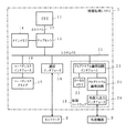
図1は、本発明の情報処理システムの実施の一形態を示す構成図である。図中、1は情報処理システム、2はネットワーク、3は外部機器、11はCPU、12はホストバス、13はチップセット、14はメインメモリ、15はシステムバス、16はハードディスクインタフェース、17はハードディスクドライブ、18は通信インタフェース、19は拡張ハードウェア部、21はプログラマブル論理回路、22はローカルメモリ、23はプログラマブル論理回路インタフェース、24は外部入出力インタフェースである。
【0029】
情報処理システム1において、CPU11のホストバス12に、チップセット13に含まれる図示しないメモリコントローラを介して、DRAMで構成されるメインメモリ14が接続されている。ホストバス12は、チップセット13に含まれる図示しないバスブリッジを介してシステムバス15に接続されている。システムバス15は、例えばPCIバスやISAバス、その他各種のバスを使用することができる。例えばシステムバス15としてPCIバスを用いた場合、チップセット13内にはホスト−PCIブリッジを備えていればよい。
【0030】
システムバス15には、この例では、ハードディスクインタフェース16を介してハードディスクドライブ17が接続され、また通信インタフェース18を介してネットワーク2と接続されている。さらに拡張ハードウェア部19が接続され、この拡張ハードウェア部19を介して外部機器3が接続されている。もちろん他の種々の機器が直接あるいはインタフェースを介してシステムバス15に接続されていてもよく、また、ハードディスクおよびネットワークについても接続は任意である。
【0031】
この例では、ハードディスクドライブ17にはアプリケーションプログラムが格納されている。アプリケーションプログラムは、ハードディスクインタフェース16、システムバス15、および、チップセット13に含まれる図示しないバスブリッジを介して、ハードディスクドライブ17からメインメモリ14にロードされてCPU11によって実行される。
【0032】
また、通信インタフェース18は、LANやインターネットなどのネットワーク2を介して、様々な機器との間でデータの転送を行うことができる。CPU11によって実行されるアプリケーションプログラムは、この通信インタフェース18を介して通信を行うことにより、ネットワーク2に接続される例えば記憶装置に格納されている情報へのアクセスを行うことができ、様々なアプリケーションプログラムやデータなどを入手できる。この場合、ネットワーク2に接続される通信インタフェース18を介して転送したアプリケーションプログラムをメインメモリ14に格納して実行したり、あるいはシステムバス15から直接プログラマブル論理回路インタフェース23を介してプログラマブル論理回路21へ転送することもできる。
【0033】
拡張ハードウェア部19は、プログラマブル論理回路21、ローカルメモリ22、プログラマブル論理回路インタフェース23を有している。またこの例では、外部入出力インタフェース24もこの拡張ハードウェア部19に設けられている。プログラマブル論理回路21は、回路情報を変更することによって機能を随時変更し再構成することが可能であり、プログラマブル論理回路インタフェース23を介してシステムバス15に接続されている。また、この例では外部入出力インタフェース24を介して外部機器3とも接続されており、プログラマブル論理回路21における処理により、外部機器3を制御可能に構成した例を示している。
【0034】
ローカルメモリ22は、プログラマブル論理回路21で処理を行う処理データや、処理後の中間処理データなどを保持することができる。また、予め使用する回路情報と順番を保持する回路情報保持手段としても機能する。
【0035】
プログラマブル論理回路インタフェース23は、システムバス15によってCPU11やメインメモリ14、ローカルメモリ22、プログラマブル論理回路21との間でデータ転送や制御を行うためのものである。またプログラマブル論理回路インタフェース23は、転送されてきた処理データからプログラマブル論理回路の再構成に使用する最初の回路情報を特定する機能を有している。この最初の回路情報が例えば処理データのヘッダ情報として付加されている場合、処理データのヘッダ情報を解釈することによって実現できる。また、回路再構成のための回路情報や処理データ、中間処理データの最後に付加されるEOFのマーカ検出機能なども含まれている。さらに、特定した最初の回路情報をもとにローカルメモリ22から回路情報を順番に取り出し、順次プログラマブル論理回路21を再構成して処理回路を構成し、構成した処理回路に処理データの処理を行わせる。また、ローカルメモリ22とプログラマブル論理回路21との間での処理データや中間処理データの転送も行う。
【0036】
なお、予め使用する回路情報等は、例えばメインメモリ14やハードディスクドライブ17に格納しておいてもよい。この場合、プログラマブル論理回路インタフェース23は、メインメモリ14やハードディスクドライブ17に対して、CPU11を動作させずにデータ転送を行う機能を有していればよい。例えばメインメモリ14とローカルメモリ22を同じメモリ空間においてアクセス可能に構成し、いずれのメモリを利用しているかを意識しないでアクセスできるように構成してもよい。
【0037】
また、拡張ハードウェア部19は、集積化により一体化することで、入出力部のライン負荷を低減させたり、専用バス化の構成により、高速化及び低消費電力化を図ることができる。
【0038】
図2は、プログラマブル論理回路の一例を示す平面構造図、図3は、同じく内部構造の一例を示すブロック図である。図中、31は論理セル、32は配線領域、33は入出力端子、41はコンフィギュレーションメモリ、42は回路素子である。プログラマブル論理回路21は、回路情報を格納するためのコンフィギュレーションメモリ41と、論理セル31や配線領域32からなる回路素子42と、入出力端子33とで構成されている。
【0039】
コンフィギュレーションメモリ41は、EEPROM、SRAMなどの書き換え可能なメモリ素子で構成されている。回路情報はアドレスとデータの対で構成される。コンフィギュレーションメモリ41にアドレスを与えて、そのアドレスに対応するメモリセルにアドレスと対になったデータを格納すると、このデータに従って、論理セル31内の回路構成や、論理セル31と入出力端子33を相互に接続する配線領域32の接続状態が再構成される。コンフィギュレーションメモリ41の一部分を書き換えることにより、プログラマブル論理回路21が動作中であっても、回路を部分的に再構成することができる。
【0040】
プログラマブル論理回路21に再構成された回路素子42に、入出力端子33を介して処理すべきデータ(処理データや中間処理データ)が入力され、また、その処理結果(中間処理データ)が出力される。データ入力先の論理セルと、データ出力元の論理セルは、論理セルの位置に対応するセル座標を示した制御コードによってアプリケーションプログラムが指定する。
【0041】
以上のシステム構成によって、プログラマブル論理回路21による処理データの入出力方法から、以下のような処理形態があげられる。データとしては、マルチメディアのような画像、音声などのストリーミングデータなどがある。
▲1▼ ネットワーク2を経由して情報システム1に入力したデータを、システムバス15を経由して、プログラマブル論理回路21に再構成した処理回路で処理する。
▲2▼ ハードディスクドライブ17などの記憶装置に格納されたデータを、システムバス15を経由して、プログラマブル論理回路21に再構成した処理回路で処理する。
▲3▼ 外部の記憶装置からの転送やアプリケーションの処理結果などのデータで、メインメモリ14に一時的に格納されたデータを、システムバス15を経由して、プログラマブル論理回路21に再構成した処理回路で処理する。
▲4▼ ローカルメモリに格納されたデータを、プログラマブル論理回路インタフェース23を経由して、プログラマブル論理回路21に再構成した処理回路で処理する。
【0042】
次に、本発明の情報処理システムの実施の一形態における動作について説明する。アプリケーションプログラムにおいて、処理のフローが決定されていて、そのために用いる機能回路が複数の種類の組み合わせであらかじめ選択指定可能な場合や、同じ順番を単位として繰り返される処理の場合などには、あらかじめ使用する回路情報と順番を決定できる。そこで、アプリケーションの処理が開始される前に、予め、使用する回路情報と順番等の情報を参照テーブルとして例えばローカルメモリ22などに登録しておく。なお、全く不定な順番で、任意の処理の次にどのような処理を行うことになるのか特定できない場合には、メインプロセッサによって、その都度、制御を行えばよいので、ここでは対象外とする。
【0043】
図4は、参照テーブルの一例の説明図である。図4に示した例では、処理回路の順番を示す処理ステップNo.に対応して、再構成のための回路情報が格納されているメモリ中の開始アドレスを示すポインタ、中間処理を行うことになる場合に対応してアロケーションされた中間処理データを格納するメモリ中の開始アドレスを示すポインタ、プログラマブル論理回路21に同時に再構成可能な回路数の情報によって参照テーブルが構成されている。
【0044】
アプリケーションの処理でi番目の処理回路で処理した結果を次のi+1番目で処理する場合には、i番目の処理回路から出力されるデータは中間処理データとなる。また最後のM番目で処理した結果は、最終出力データとなる。この中間処理データを格納するメモリの開始アドレスポインタが図4におけるポインタPdiである。なお、最終データもさらに別のアプリケーションで用いられることも考えられるので、最終データも中間処理データ用メモリへ格納しておいてもよい。
【0045】
また、再構成する処理回路について、プログラマブル論理回路の回路規模に応じて、同時に再構成できる回路数Niは、i番目の回路からの同時再構成可能最大数である。このNiに対応する回路の再構成のモードとして、1個の場合には自動的に単独コンフィギュレーションモードになり、複数個の場合には単独コンフィギュレーションモードまたは連続コンフィギュレーションモードの選択ができる。これは、アプリケーション開始時にCPUによって選択指定できる。
【0046】
この図4に示すような参照テーブルは、アプリケーションが実行されるときに情報処理システムで用いられるプログラマブル論理回路21の品種や回路規模サイズ、メインメモリ14やローカルメモリ22などのメモリサイズなどを考慮して、CPU11によって作成する。あるいは、当然ながら、決まった処理を同じシステムで行う場合には、処理の実行の都度にこの参照テーブルを作成する必要はなく、予め用意しておくこともできる。
【0047】
図5は、処理データおよび回路情報と、これらを格納するメモリアドレス空間の説明図である。図4に示すような参照テーブルの情報は、図5に示すように、例えば処理データのヘッダ部に付加しておくことができる。プログラマブル論理回路インタフェース23において、処理データを受け取った際にヘッダ部を解析し、これらの情報を取り出して、参照テーブルを作成することができる。また、このような参照テーブルをもとに、ある処理ステップiを実行する際には、処理ステップNo.iに対応付けられている回路情報用のポインタPciと中間処理データ用のポインタPdiが割り付けられる。処理の順番によっては、同じポインタを用いて上書きでアロケートすることによって、メモリの使用効率を向上させることもできる。
【0048】
なお、図5に示すメモリアドレス空間は、ローカルメモリ22のメモリアドレス空間、あるいは、メインメモリ14とローカルメモリ22を一体としたメモリアドレス空間であってよい。後者の場合、例えば回路情報や中間処理データを格納する領域などがメインメモリ14上に確保される場合もある。
【0049】
前述の回路情報と順番において、図4に示すように、処理ステップNo.として最初の0番からM番までのM+1ステップの場合で、i番目の処理を行う際の動作について述べる。再構成する回路情報を格納するメモリの開始アドレスポインタをPciとする。また、中間処理データを格納するメモリの開始アドレスポインタをPdiとする。さらに、再構成する処理回路について、プログラマブル論理回路の回路規模に応じて、同時に再構成できる回路数をNiとする。
【0050】
アプリケーションの処理データファイル及び回路情報を読み出し、あらかじめアプリケーションプログラムの実行前に、回路情報をメモリ空間に割り付けておく。また、CPU11によって前述の4種の情報をアプリケーションの処理データファイルのヘッダ部に付加する。なお、処理データファイルや回路情報は、例えば、ネットワーク2に接続された記憶装置、情報処理システム1内部のハードディスクドライブ17などの記憶装置、メインメモリ14、あるいは、ローカルメモリ22など、いずれの記憶装置に記憶されていてもよい。
【0051】
アプリケーションプログラムの実行がCPU11によって開始されると、処理データファイルがプログラマブル論理回路インタフェース23に転送されてヘッダ部に付加されている情報が解釈される。最初の回路情報によってプログラマブル論理回路21に対する処理回路の再構成が行われ、回路情報の最後を示すEOFのマーカにより、再構成が終了する。このEOFマーカをプログラマブル論理回路インタフェース23で検出し、ヘッダ部に続くデータ部の転送が行われて、再構成した処理回路におけるデータ処理が進められていく。
【0052】
処理されたデータを次に再構成する処理回路で用いる場合には、処理されたデータを中間処理データとして、さきにメモリ空間にアロケートした領域に一旦格納する。そして、次の処理回路を再構成した後、中間処理データを新たに再構成した処理回路に入力し、データ処理を進める。最終データは、例えば外部入出力インタフェース24を介して外部機器3に転送されたり、あるいはメインメモリ14,ハードディスクドライブ17,ネットワーク2に接続された記憶装置などに転送される。または、中間処理データと同様に格納されていてもよい。
【0053】
以上のように、CPU11が最初の開始制御を行うことによって、回路の再構成とデータ処理が順次実行されていくので、CPU11はプログラマブル論理回路21の再構成のための処理を行う必要がない。そのため、CPU11の負荷を軽減して消費電力を大幅に低減し、またCPU11とプログラマブル論理回路21との並行動作を可能として情報処理システムにおける全体のパフォーマンスを向上させることができる。
【0054】
次に、プログラマブル論理回路21への処理回路の再構成領域とそれぞれの処理回路によって処理された中間処理データのメモリへの格納あるいは連続処理について、以下、3つの形態をあげて説明する。
【0055】
図6は、プログラマブル論理回路への処理回路の第1の再構成例の説明図、図7は、同じく動作時の一例を示すタイミングチャートである。図6に示す例では、シングルタスクモードで、処理回路の再構成とその処理回路での処理の実行を順次行いながら、中間処理データの入出力をその間に入れていく方式を示している。この例は、プログラマブル論理回路21の構成可能な最大回路規模と再構成する回路規模との関係において、連続する処理回路が同時に再構成できる領域が確保できない場合に対応する形態である。
【0056】
最初の処理回路の再構成が完了し、データ処理が行われて得られた結果は、一時的にプログラマブル論理回路21の内部メモリまたはローカルメモリ22やメインメモリ14など外部メモリを利用して中間処理データのまま格納する。そして、最初に再構成された領域に上書きして次の処理回路の再構成を行う。次の処理回路の再構成が完了すると、続けて中間処理データに対してデータ処理を行う。このようにしてデータ処理が継続されていく。処理モードとしては、回路の同時再構成可能な数Niは、1個である単独コンフィギュレーションモードの場合である。
【0057】
一例として、図6に示す例について、図7に示すタイミングチャートを用いて説明する。まず、CPU11によって、例えば図4に示すような参照テーブルが用意され、図5に示すようにメモリアドレス空間が割り当てられる。プログラマブル論理回路インタフェース23は、CPU11から処理データが転送されてくると、その処理データのヘッダ部に付加された情報を解釈して、プログラマブル論理回路21に対する回路Aの再構成を開始する(図7−▲1▼)。
【0058】
回路Aの再構成が完了すると、処理データを回路Aに入力し、回路Aを用いた処理が開始される(図7−▲2▼)。回路Aによって得られた結果は、中間処理データとしてメモリに格納されていく(図7−▲3▼)。
【0059】
処理データのEOFが検出されて処理が終了すると、次の回路Bの再構成を行う(図7−▲4▼)。最初に再構成された回路Aの領域に上書きして次の処理回路である回路Bの再構成を行うことができる。図6は、この回路Bを再構成したときの状態を示している。回路情報のEOFが検出されると、回路Bの再構成が完了する(図7−▲5▼)。回路Bの再構成が完了すると、回路Bは中間処理データに対してデータ処理を開始する(図7−▲6▼)。
【0060】
このステップが繰り返されて、処理ステップMで終了する。このように、最初にCPU11による制御を施すだけで、あとは、処理回路の再構成と、再構成された処理回路における処理の実行が、あらかじめ設定された規定通りに連続して行われる。これによって、CPU11の制御負荷が大幅に軽減され、消費電力が大幅に低減できる。
【0061】
図8は、プログラマブル論理回路への処理回路の第1の再構成例における動作の一例を示すフローチャートである。上述の例について処理動作をまとめると図8に示すようになる。S101において処理ステップを示す変数iを0に初期化し、S102において、処理データを入力し、ヘッダ部の情報を解釈してポインタ等の設定を行う。
【0062】
S103において、回路情報Pciにアクセスしてプログラマブル論理回路21に対して処理回路の再構成を行う。S104において回路情報の終了を示すEOFを検出すると、処理回路の再構成を終了する。そしてS105において、中間処理データPd(i−1)へアクセスして再構成した処理回路に入力し、あるいは、処理データを再構成した処理回路に入力して、S106においてデータ処理を開始する。
【0063】
S107において、処理データあるいは中間処理データの終了を示すEOFを検出すると、処理回路における処理を終了する。S108において、処理ステップを示す変数iに1を加え、S109において、変数iの値がM以下か否かを判定する。変数iの値がM以下であれば、S110において、処理結果を中間処理データとして中間処理データ用のメモリ領域Pd(i−1)に格納する。そしてS103へ戻り、次の処理回路の再構成および処理を繰り返す。
【0064】
処理ステップMまでの処理を行い、処理ステップを示す変数iの値がMを超える場合には、S111において、処理後のデータを最終データとして出力し、プログラマブル論理回路21における処理を終える。
【0065】
なお、上述の説明では中間処理データを生成して処理する形態で記述したが、図2に示すように回路Aの結果を内部メモリで受けて、引き続き回路Bで処理する場合には、内部メモリの代わりに、データラッチ回路を用いた一時的なデータ保持方法の利用も可能である。
【0066】
図9は、プログラマブル論理回路への処理回路の第2の再構成例の説明図、図10は、同じく動作時の一例を示すタイミングチャートである。図9に示す例では、シングルタスクモードではあるが、複数の処理が同時に形成できる場合に、複数の処理回路の再構成を行ってから、処理を連続して実行する形態である。処理モードとして、回路の同時再構成可能な数Niまでの再構成を連続的に行う、連続コンフィギュレーションモードの選択である。
【0067】
プログラマブル論理回路21の構成可能な最大回路規模と再構成する処理回路の回路規模との関係において、連続する処理回路が同時に再構成できる領域が確保できるが、データ処理が行われて得られた結果は、一時的にプログラマブル論理回路の内部メモリまたはローカルメモリやメインメモリの外部メモリを利用して中間処理データのまま格納して行っていく場合である。ただし、中間処理データを介しながら分割して処理を進めていく場合も含めることができる。当然ながら、処理モードとして、処理回路を一つずつ再構成してゆく単独コンフィギュレーションモードも選択できる。この場合には、図6に示した形態として扱うこともできる。
【0068】
一例として、図9に示す例について、図10に示すタイミングチャートを用いて説明する。まず、CPU11によって、図4に示すような参照テーブルが用意され、図5に示すようにメモリアドレス空間が割り当てられる。プログラマブル論理回路インタフェース23は、CPU11から処理データが転送されてくると、その処理データのヘッダ部に付加された情報を解釈する。そして、プログラマブル論理回路21に再構成可能な複数個の回路、ここでは回路Aと回路Bの再構成を開始する(図10−▲1▼、▲2▼)。
【0069】
2つの回路情報のEOFが検出されると再構成を完了し、これらの処理回路を用いた処理の実行が開始される(図10−▲3▼、▲4▼)。ここでは、回路Aによって処理された結果が回路Bに入力され、回路Bによる処理結果が中間処理データとしてメモリに格納されていく。ここでは、最後の処理回路による処理結果のみを示している(図10−▲5▼、▲6▼)。
【0070】
このような処理が繰り返されて、処理ステップMで終了する。このように連続処理が可能になるため、中間処理データのすべてに対してメモリへ格納せずに処理を進めることができる。そのため、中間処理データを格納する回数が低減され、高速処理、消費電力の低減が図れる。また、最初にCPU11による制御を施すだけで、あとは、処理回路の再構成と、再構成された処理回路における処理の実行が、あらかじめ設定された規定通りに連続して行われる。これによって、CPU11の制御負荷が大幅に軽減され、消費電力が大幅に低減できる。
【0071】
図11は、プログラマブル論理回路への処理回路の第2の再構成例における動作の一例を示すフローチャートである。上述の第2の構成例について処理動作をまとめると図11に示すようになる。S121において処理ステップを示す変数iを0に初期化し、S122において、処理データを入力し、ヘッダ部の情報を解釈してポインタ等の設定を行う。
【0072】
S123において、再構成した回路数を示す変数jを0に初期化する。S124において、回路情報Pc(i+j)にアクセスしてプログラマブル論理回路21に対して処理回路の再構成を行う。S125において回路情報の終了を示すEOFを検出すると、処理回路の再構成を終了する。S126において変数jの値に1を加算し、S127において、新たな変数jの値が処理ステップiにおける同時構成可能な回路数Niより小さいか否かを判定する。新たな変数jの値がNiより小さければ、S124へ戻って、同時に再構成可能な次の処理回路の再構成を行う。変数jの値がNiに達すると、S128において、同時に再構成可能な回路数までの処理回路の再構成を終了する。
【0073】
S129において、変数iが0の場合には処理データを、また変数iが0でない場合には中間処理データPd(i+Ni−1)へアクセスして、再構成した処理回路に入力し、S130においてデータ処理を開始する。
【0074】
S131において、処理データあるいは中間処理データの終了を示すEOFを検出すると、処理回路における処理を終了する。S132において、処理ステップを示す変数iにNiを加え、S133において、新たな変数iの値がM以下か否かを判定する。変数iの値がM以下であれば、S134において、処理結果を中間処理データとして中間処理データ用のメモリ領域Pd(i+Ni−1)に格納する。そしてS123へ戻り、次の複数の処理回路の再構成および再構成した複数の処理回路による連続処理を繰り返す。
【0075】
処理ステップMまでの処理を行い、処理ステップを示す変数iの値がMを超える場合には、S135において、処理後のデータを最終データとして出力し、プログラマブル論理回路21における処理を終える。
【0076】
なお、上述の第1の再構成例と同様に、シングルタスクモードで単独コンフィギュレーションを行う場合には、それぞれの処理ステップごとに中間処理データをメモリへ格納していけばよい。連続した回路の同時構成が可能なため、連続した処理が可能になる。当然、必要に応じて中間処理データはローカルメモリ22などへ格納されてもよい。
【0077】
図12は、プログラマブル論理回路への処理回路の第3の再構成例の説明図、図13は、同じく動作時の一例を示すタイミングチャートである。図12に示す例では、マルチタスクモードとして、処理回路の再構成が完了すると処理が実行されるとともに、その処理の実行中に並行して次の処理回路の再構成がプログラマブル論理回路の別の領域に対して行われる。そして、先の処理回路による処理結果が連続して処理されたり、別のデータによる並列処理などが行われていく。例えば回路Aによるプロセス中に回路Bのコンフィギュレーションを行って処理を連続的に行っていくものである。しかも、処理回路の再構成は、プログラマブル論理回路21に同時再構成可能な数Niまでの処理回路の再構成を連続的に行う、連続コンフィギュレーションモードが選択される。
【0078】
なおこの例では、さきの処理回路の再構成が完了してデータ処理が行われているときに、次の処理回路の再構成が並列して行われていく。さきの処理回路によるデータ処理の結果は、一時的にプログラマブル論理回路21の内部メモリまたはローカルメモリ22やメインメモリ14等の外部メモリを利用して中間処理データのまま格納して、次の回路の再構成が完了したときに続けてデータ処理が継続されていく。しかし、次の処理回路の再構成が、さきの処理回路の出力までに完了する場合には、図9に示したように回路Aの出力を直接、回路Bに入力するように構成してもよい。
【0079】
一例として、図12に示す例について、図13に示すタイミングチャートを用いて説明する。まず、CPU11によって、図4に示すような参照テーブルが用意され、図5に示すようにメモリアドレス空間が割り当てられる。プログラマブル論理回路インタフェース23は、CPU11から処理データが転送されてくると、その処理データのヘッダ部に付加された情報を解釈する。プログラマブル論理回路インタフェース23は、CPU11から処理データが転送されてくると、その処理データのヘッダ部に付加された情報を解釈して、プログラマブル論理回路21に対する回路Aの再構成を開始する(図13−▲1▼)。
【0080】
回路Aに関する回路情報のEOFを検出し、回路Aの再構成が完了すると、処理データを回路Aに入力し、回路Aを用いた処理が開始される(図13−▲2▼)。回路Aによって得られた結果は、中間処理データとしてメモリに格納されていく(図13−▲3▼)。
【0081】
この回路Aにおける処理と並行して、次の回路Bの再構成を開始する(図13−▲4▼)。このような処理回路において処理を行っている間に、プログラマブル論理回路に回路の同時再構成可能な数Niまでの再構成を連続的に行うことができる。
【0082】
回路Aにおける処理において処理データのEOFを検出して処理の終了を検出するとともに、次の回路Bの再構成の終了を検出すると、回路Bにおける中間処理データを用いた処理の実行が開始される(図13−▲5▼、▲6▼)。
【0083】
このように、処理回路の再構成と、再構成した処理回路の実行の並列処理によって、処理回路の再構成による処理の待ち時間を短くして高速化を図ることができるとともに、処理を連続して実行することによる処理の高速化を図ることができる。また、最初にCPU11による制御を施すだけで、あとは、処理回路の再構成とその実行を、あらかじめ設定された規定通りに連続して行うことができる。これによって、CPU11の制御負荷が大幅に軽減され、消費電力が大幅に低減できる。
【0084】
図14は、プログラマブル論理回路への処理回路の第3の再構成例における動作の一例を示すフローチャートである。上述の第3の構成例について処理動作をまとめると図14に示すようになる。S141において処理ステップを示す変数iを0に初期化し、S142において、処理データを入力し、ヘッダ部の情報を解釈してポインタ等の設定を行う。
【0085】
S143において、回路情報Pciにアクセスしてプログラマブル論理回路21に対して処理回路の再構成を行う。S144において回路情報の終了を示すEOFを検出すると、処理回路の再構成を終了する。そしてS145において処理ステップiの処理回路の再構成が終了していることを確認後、S146において、中間処理データPd(i−1)へアクセスして再構成した処理回路に入力し、あるいは、処理データを再構成した処理回路に入力して、S147においてデータ処理を開始する。
【0086】
このような再構成された処理回路における処理の実行と並行して、S161以降の処理回路の再構成を行う。まずS161において変数iの値を変数kに待避し、S162において、再構成した回路の処理ステップを示す変数jの値をk+1に初期化する。そして、S163において、回路情報Pc(j)にアクセスしてプログラマブル論理回路21に対して、空いている領域に処理回路の再構成を行う。S164において回路情報の終了を示すEOFを検出すると、処理回路の再構成を終了する。S165において変数jの値に1を加算し、S166において、同時に再構成した回路数が、処理ステップkにおいて同時構成可能な回路数Nkより小さいか否かを判定する。この判定のために、いままで再構成した回路数+1を示す新たな変数jの値と、k+Nkの値とを比較する。新たな変数jの値がk+Nkより小さければ、S163へ戻って、同時に再構成可能な次の処理回路の再構成を行う。変数jの値がk+Nkに達すると、同時に構成可能な回路数に達したものとして、処理回路の再構成を一旦停止する。
【0087】
S167において、変数jの値がMに達していれば、すべての処理回路の再構成が終了したものとして、再構成の処理を終了する。変数jの値がM以下であれば処理を継続し、S168において、再構成が終了している処理回路のすべてにおいて処理が終了するまで待ち、その後、S161へ戻って、次の同時に構成可能な回路数だけの処理回路の再構成処理を行う。
【0088】
このような処理回路の再構成処理と並行して行われていた処理回路における処理の実行は、S148において処理データあるいは中間処理データの終了を示すEOFを検出して終了する。S149において、処理ステップを示す変数iに1を加え、S150において、新たな変数iの値がM以下か否かを判定する。変数iの値がM以下であれば、S151において、処理結果を中間処理データとして中間処理データ用のメモリ領域Pd(i−1)に格納する。そしてS145へ戻り、次の処理回路の再構成終了を確認してから、次の処理回路による連続処理を繰り返す。
【0089】
処理ステップMまでの処理を行い、処理ステップを示す変数iの値がMを超える場合には、S152において、処理後のデータを最終データとして出力し、プログラマブル論理回路21における処理を終える。
【0090】
なお、上述の説明では、処理回路の再構成を、同時に構成可能な回路数ごとに行っている。しかしこれに限らず、例えば処理が終了した処理回路の領域を順次開放してゆき、次の処理回路が構成可能な領域が確保できた時点ですぐに次の処理回路を再構成するように構成してもよい。
【0091】
上述の3つの例は、適宜組み合わせることが可能である。図15は、プログラマブル論理回路への処理回路の第4の再構成例の説明図、図16は、同じく動作時の一例を示すタイミングチャートである。この例では、最初に上述の第2の再構成例で示したように、同時に構成可能な回路数だけの処理回路の再構成を先に行っておき、その後、第3の再構成例で示したように、処理が終了した処理回路の領域を開放して新たな処理回路の再構成を行うことができる。
【0092】
一例として、図15に示す例について、図16に示すタイミングチャートを用いて説明する。まず、図15(A)に示すように、プログラマブル論理回路21に再構成可能な複数個の回路、ここでは回路Aと回路Bの再構成を開始する(図16−▲1▼、▲2▼)。
【0093】
2つの回路情報のEOFが検出されると再構成を完了し、これらの処理回路を用いた処理の実行を開始する(図16−▲3▼、▲4▼)。ここでは、回路Aによって処理された結果が回路Bに入力され、回路Bによる処理結果が中間処理データとしてメモリに格納されていく(図16−▲5▼、▲6▼)。
【0094】
回路Aの処理が終了した時点で、回路Aが配置されていたプログラマブル論理回路21内の領域は不要となる。そのため、回路Bの処理実行中に並行して、回路Aが構成されていた領域も用いて、回路Cの再構成を開始する(図16−▲7▼)。このような処理回路の再構成は、処理回路を配置可能であればいくつでも行ってよい。このようにして、図15(B)に示すように、回路Aが配置されていた領域も用いて回路Cの再構成が行われる。
【0095】
回路Bにおける処理において処理データのEOFを検出して処理の終了を検出するとともに、次の回路Cの再構成の終了を検出すると、回路Bから出力された中間処理データを用いて、回路Cにおける処理の実行が開始される(図16−▲8▼、▲9▼)。このような処理が繰り返されて、処理ステップMまでの処理を連続して行うことができる。
【0096】
なお、上述の説明では、図1に示した構成をもとにして説明してきた。本発明の情報処理システムは図1に示す構成に限られることはなく、種々の変形が可能である。そのうちのいくつかの変形例については既に述べた。さらに極端な例として、例えば拡張ハードウェア部19の部分のみの構成や、さらには外部入出力インタフェース24も設けず、プログラマブル論理回路インタフェース23を介してのみデータの入出力を行う構成などであってもよい。
【0097】
【発明の効果】
以上の説明から明らかなように、本発明によれば、あらかじめ使用する回路と順番を規定できる場合には、メインプロセッサによる最初のデータ処理開始の制御だけで、あとは処理データ(例えば処理データのヘッダ情報)を解釈するだけで、プログラマブル論理回路の複数の機能回路によるデータ処理を順次実行してゆくことができる。このため、メインプロセッサによる制御の処理ステップを削減して高速化を図ることができるとともに、消費電力も低減することができる。
【0098】
また、回路の再構成のための制御に対するメインプロセッサの負荷が軽減されることによって、その処理パワーを他の処理へ使用できるため、システム全体のパフォーマンスの向上を図ることができるという効果がある。
【図面の簡単な説明】
【図1】本発明の情報処理システムの実施の一形態を示す構成図である。
【図2】プログラマブル論理回路の一例を示す平面構造図である。
【図3】プログラマブル論理回路の内部構造の一例を示すブロック図である。
【図4】参照テーブルの一例の説明図である。
【図5】処理データおよび回路情報と、これらを格納するメモリアドレス空間の説明図である。
【図6】プログラマブル論理回路への処理回路の第1の再構成例の説明図である。
【図7】プログラマブル論理回路への処理回路の第1の再構成例における動作時の一例を示すタイミングチャートである。
【図8】プログラマブル論理回路への処理回路の第1の再構成例における動作の一例を示すフローチャートである。
【図9】プログラマブル論理回路への処理回路の第2の再構成例の説明図である。
【図10】プログラマブル論理回路への処理回路の第2の再構成例における動作時の一例を示すタイミングチャートである。
【図11】プログラマブル論理回路への処理回路の第2の再構成例における動作の一例を示すフローチャートである。
【図12】プログラマブル論理回路への処理回路の第3の再構成例の説明図である。
【図13】プログラマブル論理回路への処理回路の第3の再構成例における動作時の一例を示すタイミングチャートである。
【図14】プログラマブル論理回路への処理回路の第3の再構成例における動作の一例を示すフローチャートである。
【図15】プログラマブル論理回路への処理回路の第4の再構成例の説明図である。
【図16】プログラマブル論理回路への処理回路の第4の再構成例における動作時の一例を示すタイミングチャートである。
【図17】従来の情報処理システムの一例を示すブロック図である。
【図18】DPGAの論理セル構造の一例の説明図である。
【符号の説明】
1…情報処理システム、2…ネットワーク、3…外部機器、11…CPU、12…ホストバス、13…チップセット、14…メインメモリ、15…システムバス、16…ハードディスクインタフェース、17…ハードディスクドライブ、18…通信インタフェース、19…拡張ハードウェア部、21…プログラマブル論理回路、22…ローカルメモリ、23…プログラマブル論理回路インタフェース、24…外部入出力インタフェース、31…論理セル、32…配線領域、33…入出力端子、41…コンフィギュレーションメモリ、42…回路素子、51…アプリケーションサーバ、52,53…クライアントコンピュータ、54…通信ネットワーク、55…メインプロセッサ、56…拡張ハードウェア、57…アプリケーションプログラム、58…拡張コード、59…メインプロセッサコード、60…OS、61…コード選択機能、71…DRAM、72,75…マルチプレクサ、73…ルックアップテーブル、74…フリップフロップ。[0001]
TECHNICAL FIELD OF THE INVENTION
The present invention relates to an information processing apparatus capable of processing a part of processing by an application program by a programmable logic circuit whose circuit configuration can be reconfigured. In particular, the present invention relates to a method for continuously executing circuit reconfiguration and processing.
[0002]
[Prior art]
2. Description of the Related Art In the field of digital circuit devices, particularly application-specific integrated circuits (ASICs), in order to reduce product development time, programmable logic circuits including field programmable gate arrays (FPGAs) and programmable logic devices (PLDs) have been developed. Widely used. These programmable logic circuits can freely configure internal logic circuits and connections between the logic circuits by reading circuit information describing the logic circuits. For this reason, using a programmable logic circuit has the advantage that the time required to manufacture an integrated circuit, which conventionally required several weeks to several months after the completion of circuit design, is not required. In particular, an electrically reconfigurable programmable logic device as described in, for example, U.S. Pat. No. 4,700,187 can freely change a circuit once manufactured as many times as necessary. It has the advantage of being used more and more widely.
[0003]
By the way, recent logic circuits are becoming more and more complicated, and the circuit scale is increased to a size that cannot be realized by one programmable logic circuit. As one method for solving this problem, it has been proposed to reconfigure a programmable logic circuit during processing in order to realize different logic circuits at different times. By using this method, there is an advantage that various processes can be performed at relatively high speed even when the size of a circuit that can be built in is limited due to the small size of the device such as a portable information terminal.
[0004]
However, when reconfiguring the programmable logic circuit, it is necessary to read the circuit information of the entire circuit again, so that there is a disadvantage that the reconfiguration takes time. Further, reconfiguring in the middle of the process means that the process is temporarily suspended, the data at that time is saved in a storage device outside the programmable logic circuit, new circuit information is read and reconfigured, and the data before the reconfiguration is reconstructed. And extra processing of inputting new data accompanying the reconstruction is required.
[0005]
In order to solve this problem, for example, a programmable logic circuit described in a data book named “CONFIGUABLE LOGIC” of Atmel, USA, and a data book named “THE PROGRAMMABLELOGIC” of Xilinx, Inc. in the United States are described. There are programmable logic circuits and the like. These programmable logic circuits have a data storage device for storing data, and can read part of the circuit information from an external storage device and partially reconfigure the circuit even during operation of the circuit. This minimizes the time for reconfiguration.
[0006]
When such a programmable logic circuit is used in an information processing system, there is a problem that, for example, a control device such as a CPU must perform processing of an application and the like and reconfiguration of the programmable logic circuit at high speed and efficiently. That is, the control device extracts circuit information for forming a desired logic circuit from a storage destination, combines a plurality of pieces of circuit information as necessary, and reconfigures the desired logic circuit in the programmable logic circuit. In parallel with this, it is necessary to execute the processing of the application, and both processing must be performed at high speed and efficiently.
[0007]
The information system that performs processing while reconfiguring a programmable logic circuit based on a plurality of circuit information described above can be used by connecting to a network. As an example, there is a “reconfigurable network computer” disclosed in Japanese Patent Application Laid-Open No. 10-78932.
[0008]
FIG. 17 is a block diagram illustrating an example of a conventional information processing system. In the figure, 51 is an application server, 52 and 53 are client computers, 54 is a communication network, 55 is a main processor, 56 is extended hardware, 57 is an application program, 58 is an extended code, 59 is a main processor code, and 60 is an OS , 61 are code selection functions. The information processing system includes a plurality of computers connected by a communication network 54.
[0009]
The application server 51 is a computer that distributes application programs. Further, the
[0010]
In the
[0011]
The
[0012]
In another configuration, the function realized by the
[0013]
Further, the
[0014]
If the configuration of the programmable logic circuit constituting the
[0015]
A hardware resource management function for reusing the unnecessary hardware resources for another application program so that a plurality of applications using the extended
[0016]
As described above, when an application program distributed from an application server is executed on a client computer side on a computer connected via a network, functions are changed as needed by the program, and reconfigurable extended hardware is provided to the client computer. Mount. Then, the application program stored in the application server includes a main processor code and an extension code. At the time of execution, the configuration of the extended hardware is changed on the client computer side by a code selection function of the OS which determines the presence / absence and type of the extended hardware, so that the configuration is suitable for processing. This allows the client computer to process the application program at high speed.
[0017]
Conventionally, when a new service requiring special hardware on the client computer side is to be started on the network, the user on the client computer side has to introduce new hardware for that purpose. Also, service providers have provided new services only to some users who have new hardware. However, as described above, in a configuration that has extended hardware with programmable logic circuits, a new service can be started without introducing new hardware by reconfiguring the programmable logic circuits. It becomes.
[0018]
As described above, when the processing is executed while reconfiguring the circuit by using the programmable logic circuit as the extended hardware, control by the CPU is required. For example, a processing method in which the main processor is always operated is used even when a processing flow is determined in an application program and a functional circuit used for the processing can be selected and designated in advance. In particular, when extended hardware is installed in the client computer as in the above-described system example, control for reconfiguring by extended code is performed by the main processor of the client computer. Therefore, a necessary extension code is associated with the main program of the application program in advance, and each time the extension hardware is reconfigured, the extension is performed by using the extension code under the control of the main processor. For this reason, when executing application programs while frequently reconfiguring various types of extended hardware, the main processor must always monitor the progress of processing and perform control for reconfiguration. There is a disadvantage that the load on the main processor increases. Further, it is necessary to operate the main processor together with the operation of the extended hardware, and there is a disadvantage that the power consumption of the entire client increases.
[0019]
As described above, since the processing load of the main processor is constantly generated by the control for reconfiguring the circuit, there is a problem that the power consumption is increased by combining the main processor and the extended hardware. In addition, there is a disadvantage that the performance of the entire system is reduced due to the load of the main processor for reconfiguring the circuit.
[0020]
Next, a new device technology for a programmable logic circuit will be described. 2. Description of the Related Art Programmable logic circuits have begun to be used in reconfigurable computing, in which processing circuits adapted to the processing of applications are configured on programmable logic circuits and high-speed processing is realized using the dedicated processing circuits. In reconfigurable computing, circuit information of a plurality of processing circuits required for application processing is stored in a storage device in advance, and the circuit information read from the storage device is written to a programmable logic circuit as needed. , And generate a circuit required at that time. This technology is called cache logic technology or virtual logic technology.
[0021]
The cache logic technology is a time-division driving technology in which different circuits are configured as needed on the same programmable logic circuit. As a result, by using a programmable logic circuit having a small circuit scale, a circuit larger than the circuit scale can be realized, and the size and cost of the circuit device can be reduced. However, depending on the scale of the circuit information written in the programmable logic circuit, there is a problem that the reconfiguration time of the circuit becomes longer and the effect of the reconfigurable computing of realizing high-speed processing using a dedicated processing circuit is impaired. .
[0022]
One solution to this problem is a device technology called multi-context technology. That is, a memory for storing a plurality of pieces of circuit information is provided in the programmable logic circuit, and the memory is switched as necessary to reconfigure the circuit, so that the reconfiguration time of the circuit can be significantly reduced.
[0023]
One of the conventional examples of the multi-context technique is the DPGA indicated by “A First Generation DPGA Implementation” of FPD'95. FIG. 18 is an explanatory diagram of an example of the logic cell structure of the DPGA. In the figure, 71 is a DRAM, 72 and 75 are multiplexers, 73 is a look-up table, and 74 is a flip-flop. As shown in FIG. 18, the DPGA logic cell includes a 4 × 32
[0024]
Multi-context techniques can significantly reduce circuit reconfiguration time. Further, the load on the input / output bus lines when transferring circuit information for reconfiguring the circuit to the programmable logic circuit can be reduced, which is advantageous for high speed and low power consumption. However, a memory circuit area for storing circuit information needs to be integrally formed with the programmable logic circuit, and there is a disadvantage that the circuit scale of the entire programmable logic circuit when integrated is increased.
[0025]
[Problems to be solved by the invention]
The present invention has been made in view of the above circumstances, and can significantly reduce the load on a main processor for reconfiguring a programmable logic circuit, thereby reducing power consumption and reducing the main processor. It is an object of the present invention to provide an information processing apparatus that can be effectively used to improve the performance of the entire system.
[0026]
[Means for Solving the Problems]
Generally, in an application program, a processing flow is determined, and when a processing circuit used for the processing can be selected and designated in advance by a combination of a plurality of types, in a case where the processing is repeated repeatedly in the same order as a unit, for example, The circuit information to be used and the order can be determined. The present invention makes use of this, and causes the circuit information holding means to sequentially hold circuit information for configuring the processing circuit in the programmable logic circuit. Then, a control unit such as a CPU requests a process including information for specifying circuit information to be used, for example, in a header portion of processing data to be processed by the programmable logic circuit. The interface means specifies the first circuit information to be used for the reconfiguration of the programmable logic circuit from, for example, a header portion of the given processing data, and determines the order in which the circuit information is held in the circuit information holding means from the specified circuit information. Then, circuit information is extracted, a programmable logic circuit is reconfigured to configure a processing circuit, and the configured processing circuit processes the processing data.
[0027]
Thus, in the programmable logic circuit, the reconfiguration and execution of the processing circuit are automatically performed in a preset order. Therefore, the control means such as the CPU only issues the execution instruction first, and does not need to issue the reconfiguration or execution instruction of the programmable logic circuit which is performed in order thereafter. As a result, the number of processing steps for controlling the programmable logic circuit by the control means such as the CPU can be greatly reduced, the speed can be increased, and the power consumption can be significantly reduced. At the same time, the overall performance of the information processing device including the programmable logic circuit can be improved.
[0028]
BEST MODE FOR CARRYING OUT THE INVENTION
FIG. 1 is a configuration diagram showing an embodiment of the information processing system of the present invention. In the figure, 1 is an information processing system, 2 is a network, 3 is an external device, 11 is a CPU, 12 is a host bus, 13 is a chipset, 14 is a main memory, 15 is a system bus, 16 is a hard disk interface, and 17 is a hard disk A drive, 18 is a communication interface, 19 is an extended hardware unit, 21 is a programmable logic circuit, 22 is a local memory, 23 is a programmable logic circuit interface, and 24 is an external input / output interface.
[0029]
In the
[0030]
In this example, a hard disk drive 17 is connected to the
[0031]
In this example, the hard disk drive 17 stores an application program. The application program is loaded from the hard disk drive 17 to the
[0032]
The
[0033]
The extended hardware unit 19 has a
[0034]
The
[0035]
The programmable
[0036]
The circuit information used in advance may be stored in the
[0037]
Further, the extension hardware unit 19 can be integrated so as to reduce the line load of the input / output unit, and can achieve high speed and low power consumption by using a dedicated bus.
[0038]
FIG. 2 is a plan view showing an example of the programmable logic circuit, and FIG. 3 is a block diagram showing an example of the internal structure. In the figure, 31 is a logic cell, 32 is a wiring area, 33 is an input / output terminal, 41 is a configuration memory, and 42 is a circuit element. The
[0039]
The configuration memory 41 is configured by a rewritable memory element such as an EEPROM and an SRAM. The circuit information is composed of address and data pairs. When an address is given to the configuration memory 41 and the data paired with the address is stored in the memory cell corresponding to the address, the circuit configuration in the
[0040]
Data to be processed (processing data or intermediate processing data) is input to the
[0041]
With the above system configuration, the following processing modes can be cited from the input / output method of processing data by the
(1) The data input to the
(2) Data stored in a storage device such as the hard disk drive 17 is processed by the processing circuit reconfigured in the
{Circle around (3)} Process of reconfiguring data temporarily stored in the
(4) The data stored in the local memory is processed by the processing circuit reconfigured in the
[0042]
Next, an operation of the information processing system according to the embodiment of the present invention will be described. If the flow of processing is determined in the application program and the functional circuit used for that can be selected and specified in advance by a combination of a plurality of types, or if the processing is repeated in the same order as a unit, it is used in advance. Circuit information and order can be determined. Therefore, before the processing of the application is started, circuit information to be used and information such as an order are registered in advance in the
[0043]
FIG. 4 is an explanatory diagram of an example of the reference table. In the example shown in FIG. 4, the processing step No. indicating the order of the processing circuits. A pointer indicating the start address in the memory in which the circuit information for the reconfiguration is stored, and a pointer in the memory for storing the intermediate processing data allocated corresponding to the case where the intermediate processing is to be performed. A reference table is constituted by a pointer indicating a start address and information on the number of circuits that can be simultaneously reconfigured in the
[0044]
In the case of processing the result processed by the i-th processing circuit in the next (i + 1) -th processing in the application processing, data output from the i-th processing circuit is intermediate processing data. The result of processing at the last M-th becomes final output data. The start address pointer of the memory storing the intermediate processing data is the pointer Pdi in FIG. Since the final data may be used by another application, the final data may be stored in the intermediate processing data memory.
[0045]
Further, the number of circuits Ni that can be simultaneously reconfigured for the processing circuit to be reconfigured according to the circuit scale of the programmable logic circuit is the maximum number of simultaneously reconfigurable circuits from the i-th circuit. As a mode for reconfiguring the circuit corresponding to Ni, the single configuration mode is automatically set in the case of one, and the single configuration mode or the continuous configuration mode can be selected in the case of a plurality. This can be selected and designated by the CPU at the start of the application.
[0046]
The reference table as shown in FIG. 4 takes into account the type and size of the
[0047]
FIG. 5 is an explanatory diagram of processing data and circuit information, and a memory address space for storing them. The information of the reference table as shown in FIG. 4 can be added, for example, to the header of the processing data as shown in FIG. In the programmable
[0048]
The memory address space shown in FIG. 5 may be a memory address space of the
[0049]
In the order of the circuit information described above, as shown in FIG. In the case of the first M + 1 steps from the 0th to the Mth, the operation at the time of performing the i-th process will be described. Let Pci be the start address pointer of the memory that stores the circuit information to be reconfigured. The start address pointer of the memory for storing the intermediate processing data is Pdi. Further, regarding the processing circuit to be reconfigured, the number of circuits that can be reconfigured simultaneously according to the circuit scale of the programmable logic circuit is assumed to be Ni.
[0050]
The processing data file and the circuit information of the application are read out, and the circuit information is allocated to the memory space before executing the application program. Further, the
[0051]
When the execution of the application program is started by the
[0052]
When the processed data is used in a processing circuit for reconstructing the next data, the processed data is temporarily stored as intermediate processing data in the area allocated in the memory space. Then, after reconfiguring the next processing circuit, the intermediate processing data is input to the newly reconfigured processing circuit, and the data processing proceeds. The final data is transferred to the
[0053]
As described above, the reconfiguration of the circuit and the data processing are sequentially performed by the
[0054]
Next, the reconfiguration area of the processing circuit in the
[0055]
FIG. 6 is an explanatory diagram of a first example of reconfiguration of a processing circuit into a programmable logic circuit, and FIG. 7 is a timing chart showing an example of the same operation. In the example shown in FIG. 6, in the single task mode, while the reconfiguration of the processing circuit and the execution of the processing by the processing circuit are sequentially performed, the input / output of the intermediate processing data is inserted therebetween. This example is a mode corresponding to a case where an area where continuous processing circuits can be simultaneously reconfigured cannot be secured in the relationship between the maximum configurable circuit size of the
[0056]
After the reconfiguration of the first processing circuit is completed and the data processing is performed, the result obtained is temporarily stored in an internal memory of the
[0057]
As an example, the example shown in FIG. 6 will be described with reference to the timing chart shown in FIG. First, the
[0058]
When the reconfiguration of the circuit A is completed, processing data is input to the circuit A, and processing using the circuit A is started (FIG. 7- (2)). The result obtained by the circuit A is stored in the memory as intermediate processing data (FIG. 7-3).
[0059]
When the EOF of the processing data is detected and the processing ends, the next circuit B is reconfigured (FIG. 7- (4)). The circuit B, which is the next processing circuit, can be reconfigured by overwriting the area of the circuit A reconfigured first. FIG. 6 shows a state when the circuit B is reconfigured. When the EOF of the circuit information is detected, the reconfiguration of the circuit B is completed (FIG. 7- (5)). When the reconfiguration of the circuit B is completed, the circuit B starts data processing on the intermediate processing data (FIG. 7-6).
[0060]
This step is repeated and ends in processing step M. As described above, only the control by the
[0061]
FIG. 8 is a flowchart illustrating an example of an operation in a first example of reconfiguring the processing circuit to the programmable logic circuit. FIG. 8 summarizes the processing operations of the above example. In step S101, a variable i indicating a processing step is initialized to 0. In step S102, processing data is input, and information of a header portion is interpreted to set a pointer and the like.
[0062]
In S103, the circuit information Pci is accessed to reconfigure the processing circuit in the
[0063]
When the EOF indicating the end of the processing data or the intermediate processing data is detected in S107, the processing in the processing circuit ends. In S108, 1 is added to the variable i indicating the processing step, and in S109, it is determined whether the value of the variable i is M or less. If the value of the variable i is equal to or less than M, in S110, the processing result is stored as intermediate processing data in the memory area Pd (i-1) for intermediate processing data. Then, the process returns to S103 to repeat the reconfiguration and processing of the next processing circuit.
[0064]
The processing up to the processing step M is performed, and when the value of the variable i indicating the processing step exceeds M, the processed data is output as final data in S111, and the processing in the
[0065]
In the above description, the intermediate processing data is generated and processed. However, as shown in FIG. 2, when the result of the circuit A is received by the internal memory and is subsequently processed by the circuit B, the internal memory is processed. Instead, a temporary data holding method using a data latch circuit can be used.
[0066]
FIG. 9 is an explanatory diagram of a second example of reconfiguration of a processing circuit into a programmable logic circuit, and FIG. 10 is a timing chart showing an example of the same operation. In the example illustrated in FIG. 9, although the single task mode is set, when a plurality of processes can be simultaneously formed, the processes are continuously executed after reconfiguring a plurality of processing circuits. The processing mode is a selection of a continuous configuration mode in which reconfiguration of a circuit up to a number Ni that can be simultaneously reconfigured is continuously performed.
[0067]
In the relationship between the maximum configurable circuit size of the
[0068]
As an example, an example shown in FIG. 9 will be described with reference to a timing chart shown in FIG. First, the
[0069]
When the EOF of the two pieces of circuit information is detected, the reconstruction is completed, and the execution of the processing using these processing circuits is started (FIG. 10- (3), (4)). Here, the result processed by the circuit A is input to the circuit B, and the processing result by the circuit B is stored in the memory as intermediate processing data. Here, only the processing result by the last processing circuit is shown (FIG. 10- (5), (6)).
[0070]
Such processing is repeated, and ends in processing step M. As described above, continuous processing can be performed, so that processing can be performed without storing all of the intermediate processing data in the memory. Therefore, the number of times of storing the intermediate processing data is reduced, and high-speed processing and power consumption can be reduced. Further, only the control by the
[0071]
FIG. 11 is a flowchart illustrating an example of an operation in a second example of reconfiguring the processing circuit to the programmable logic circuit. FIG. 11 summarizes the processing operations of the second configuration example described above. In step S121, a variable i indicating a processing step is initialized to 0. In step S122, processing data is input, and information of a header portion is interpreted to set a pointer and the like.
[0072]
In S123, a variable j indicating the number of reconfigured circuits is initialized to 0. In S124, the circuit information Pc (i + j) is accessed to reconfigure the processing circuit for the
[0073]
In step S129, if the variable i is 0, the processing data is accessed. If the variable i is not 0, the intermediate processing data Pd (i + Ni-1) is accessed and input to the reconfigured processing circuit. Start processing.
[0074]
When the EOF indicating the end of the processing data or the intermediate processing data is detected in S131, the processing in the processing circuit ends. In S132, Ni is added to the variable i indicating the processing step, and in S133, it is determined whether the value of the new variable i is M or less. If the value of the variable i is equal to or less than M, in S134, the processing result is stored as intermediate processing data in the memory area Pd (i + Ni-1) for intermediate processing data. Then, the process returns to S123, and reconfiguration of the next plurality of processing circuits and continuous processing by the reconfigured processing circuits are repeated.
[0075]
The processing up to the processing step M is performed, and if the value of the variable i indicating the processing step exceeds M, the processed data is output as final data in S135, and the processing in the
[0076]
As in the case of the first reconfiguration example, when performing the single configuration in the single task mode, the intermediate processing data may be stored in the memory for each processing step. Since a continuous circuit can be simultaneously configured, continuous processing can be performed. Of course, the intermediate processing data may be stored in the
[0077]
FIG. 12 is an explanatory diagram of a third example of reconfiguration of a processing circuit into a programmable logic circuit, and FIG. 13 is a timing chart showing an example of the same operation. In the example shown in FIG. 12, in the multitask mode, the processing is executed when the reconfiguration of the processing circuit is completed, and the reconfiguration of the next processing circuit is performed in parallel with the other of the programmable logic circuit during the execution of the processing. Performed on the region. Then, the processing results obtained by the previous processing circuit are continuously processed, and parallel processing using different data is performed. For example, the configuration of the circuit B is performed during the process by the circuit A, and the processing is continuously performed. In addition, for the reconfiguration of the processing circuit, a continuous configuration mode in which the reconfiguration of the processing circuit up to the number Ni that can be simultaneously reconfigured in the
[0078]
In this example, when the reconfiguration of the previous processing circuit is completed and the data processing is being performed, the reconfiguration of the next processing circuit is performed in parallel. The result of the data processing by the previous processing circuit is temporarily stored as intermediate processing data using the internal memory of the
[0079]
As an example, an example shown in FIG. 12 will be described with reference to a timing chart shown in FIG. First, the
[0080]
When the EOF of the circuit information relating to the circuit A is detected and the reconfiguration of the circuit A is completed, the processing data is input to the circuit A, and the processing using the circuit A is started (FIG. 13- (2)). The result obtained by the circuit A is stored in the memory as intermediate processing data (FIG. 13- (3)).
[0081]
In parallel with the processing in the circuit A, the reconfiguration of the next circuit B is started (FIG. 13-4). While processing is being performed in such a processing circuit, reconfiguration of the programmable logic circuit up to the number Ni that allows simultaneous reconfiguration of the circuit can be performed continuously.
[0082]
In the processing in the circuit A, when the end of the processing is detected by detecting the EOF of the processing data and the completion of the reconfiguration of the next circuit B is detected, the execution of the processing using the intermediate processing data in the circuit B is started. (FIG. 13- (5), (6)).
[0083]
As described above, the parallel processing of the reconfiguration of the processing circuit and the execution of the reconfigured processing circuit can shorten the waiting time of the processing by the reconfiguration of the processing circuit, increase the speed, and continuously execute the processing. The speed of the process can be increased by executing the process. Further, only by performing the control by the
[0084]
FIG. 14 is a flowchart illustrating an example of an operation in a third example of reconfiguring the processing circuit to the programmable logic circuit. FIG. 14 summarizes the processing operations of the third configuration example described above. In step S141, a variable i indicating a processing step is initialized to 0, and in step S142, processing data is input, information of a header portion is interpreted, and a pointer and the like are set.
[0085]
In S143, the processing information is reconfigured for the
[0086]
In parallel with the execution of the processing in the reconfigured processing circuit, the reconfiguration of the processing circuit from S161 is performed. First, in step S161, the value of the variable i is saved to the variable k, and in step S162, the value of the variable j indicating the processing step of the reconfigured circuit is initialized to k + 1. Then, in S163, the circuit information Pc (j) is accessed to reconfigure the processing circuit in the vacant area for the
[0087]
If the value of the variable j has reached M in S167, it is determined that the reconfiguration of all the processing circuits has been completed, and the reconfiguration processing is terminated. If the value of the variable j is equal to or less than M, the process is continued, and in S168, the process waits until the process is completed in all the processing circuits for which reconfiguration has been completed, and then returns to S161 to enable the next simultaneous configuration. The reconfiguration processing of the processing circuits corresponding to the number of circuits is performed.
[0088]
The execution of the processing in the processing circuit, which has been performed in parallel with the reconfiguration processing of the processing circuit, ends in S148 after detecting the EOF indicating the end of the processing data or the intermediate processing data. In S149, 1 is added to the variable i indicating the processing step, and in S150, it is determined whether the value of the new variable i is M or less. If the value of the variable i is equal to or less than M, in S151, the processing result is stored as intermediate processing data in the memory area Pd (i-1) for intermediate processing data. Then, the process returns to S145, and after confirming the end of the reconfiguration of the next processing circuit, the continuous processing by the next processing circuit is repeated.
[0089]
The processing up to the processing step M is performed, and when the value of the variable i indicating the processing step exceeds M, the processed data is output as final data in S152, and the processing in the
[0090]
In the above description, the reconfiguration of the processing circuit is performed for each number of circuits that can be simultaneously configured. However, the present invention is not limited to this. For example, the area of the processing circuit for which processing has been completed is sequentially opened, and the next processing circuit is reconfigured immediately when an area configurable for the next processing circuit is secured. May be.
[0091]
The above three examples can be appropriately combined. FIG. 15 is an explanatory diagram of a fourth example of reconfiguration of a processing circuit into a programmable logic circuit, and FIG. 16 is a timing chart illustrating an example of the same operation. In this example, first, as shown in the above-described second reconfiguration example, the reconfiguration of the processing circuits for the number of circuits that can be simultaneously configured is performed first, and then, in the third reconfiguration example, As described above, a new processing circuit can be reconfigured by opening the area of the processing circuit where the processing has been completed.
[0092]
As an example, an example shown in FIG. 15 will be described with reference to a timing chart shown in FIG. First, as shown in FIG. 15A, reconfiguration of a plurality of circuits reconfigurable into the
[0093]
When the EOF of the two pieces of circuit information is detected, the reconstruction is completed, and the execution of the processing using these processing circuits is started (FIG. 16- (3), (4)). Here, the result processed by the circuit A is input to the circuit B, and the processing result by the circuit B is stored in the memory as intermediate processing data (FIG. 16- (5), (6)).
[0094]
When the processing of the circuit A is completed, the area in the
[0095]
In the processing in the circuit B, the end of the processing is detected by detecting the EOF of the processing data, and when the end of the reconfiguration of the next circuit C is detected, the intermediate processing data output from the circuit B is used to detect the end of the processing. Execution of the process is started (FIGS. 16- (8) and (9)). Such processing is repeated, and the processing up to the processing step M can be continuously performed.
[0096]
Note that the above description has been made based on the configuration shown in FIG. The information processing system of the present invention is not limited to the configuration shown in FIG. 1 and various modifications are possible. Some of them have already been described. As a further extreme example, for example, a configuration of only the extension hardware unit 19 or a configuration in which the external input /
[0097]
【The invention's effect】
As is apparent from the above description, according to the present invention, when the circuit to be used and the order can be defined in advance, only the control of the start of the first data processing by the main processor is performed, and the processing data (for example, the processing data Only by interpreting the header information, the data processing by the plurality of functional circuits of the programmable logic circuit can be sequentially executed. Therefore, the number of processing steps of control by the main processor can be reduced to increase the speed, and the power consumption can be reduced.
[0098]
In addition, since the load on the main processor for control for circuit reconfiguration is reduced, the processing power can be used for other processing, thereby improving the performance of the entire system.
[Brief description of the drawings]
FIG. 1 is a configuration diagram showing an embodiment of an information processing system of the present invention.
FIG. 2 is a plan view showing an example of a programmable logic circuit.
FIG. 3 is a block diagram illustrating an example of an internal structure of a programmable logic circuit.
FIG. 4 is an explanatory diagram of an example of a reference table.
FIG. 5 is an explanatory diagram of processing data and circuit information, and a memory address space for storing them.
FIG. 6 is an explanatory diagram of a first reconfiguration example of a processing circuit for a programmable logic circuit;
FIG. 7 is a timing chart showing an example of an operation in a first reconfiguration example of a processing circuit for a programmable logic circuit;
FIG. 8 is a flowchart illustrating an example of an operation in a first reconfiguration example of a processing circuit for a programmable logic circuit;
FIG. 9 is an explanatory diagram of a second reconfiguration example of a processing circuit for a programmable logic circuit;
FIG. 10 is a timing chart showing an example of an operation in a second reconfiguration example of a processing circuit for a programmable logic circuit;
FIG. 11 is a flowchart illustrating an example of an operation in a second example of reconfiguring the processing circuit to the programmable logic circuit;
FIG. 12 is an explanatory diagram of a third reconfiguration example of a processing circuit for a programmable logic circuit;
FIG. 13 is a timing chart illustrating an example of an operation in a third example of reconfiguration of the processing circuit to the programmable logic circuit;
FIG. 14 is a flowchart illustrating an example of an operation in a third example of reconfiguring the processing circuit to the programmable logic circuit;
FIG. 15 is an explanatory diagram of a fourth reconfiguration example of a processing circuit for a programmable logic circuit;
FIG. 16 is a timing chart showing an example of an operation in a fourth reconfiguration example of a processing circuit for a programmable logic circuit;
FIG. 17 is a block diagram illustrating an example of a conventional information processing system.
FIG. 18 is an explanatory diagram of an example of a logic cell structure of a DPGA.
[Explanation of symbols]
DESCRIPTION OF
Claims (7)
Priority Applications (1)
| Application Number | Priority Date | Filing Date | Title |
|---|---|---|---|
| JP23838499A JP3587095B2 (en) | 1999-08-25 | 1999-08-25 | Information processing equipment |
Applications Claiming Priority (1)
| Application Number | Priority Date | Filing Date | Title |
|---|---|---|---|
| JP23838499A JP3587095B2 (en) | 1999-08-25 | 1999-08-25 | Information processing equipment |
Publications (3)
| Publication Number | Publication Date |
|---|---|
| JP2001068993A JP2001068993A (en) | 2001-03-16 |
| JP2001068993A5 JP2001068993A5 (en) | 2004-10-28 |
| JP3587095B2 true JP3587095B2 (en) | 2004-11-10 |
Family
ID=17029401
Family Applications (1)
| Application Number | Title | Priority Date | Filing Date |
|---|---|---|---|
| JP23838499A Expired - Fee Related JP3587095B2 (en) | 1999-08-25 | 1999-08-25 | Information processing equipment |
Country Status (1)
| Country | Link |
|---|---|
| JP (1) | JP3587095B2 (en) |
Families Citing this family (35)
| Publication number | Priority date | Publication date | Assignee | Title |
|---|---|---|---|---|
| US6434687B1 (en) * | 1997-12-17 | 2002-08-13 | Src Computers, Inc. | System and method for accelerating web site access and processing utilizing a computer system incorporating reconfigurable processors operating under a single operating system image |
| JP3561506B2 (en) * | 2001-05-10 | 2004-09-02 | 東京エレクトロンデバイス株式会社 | Arithmetic system |
| DE10139610A1 (en) | 2001-08-11 | 2003-03-06 | Daimler Chrysler Ag | Universal computer architecture |
| FR2838208B1 (en) * | 2002-04-03 | 2005-03-11 | Centre Nat Rech Scient | LOGICAL CALCULATION ARCHITECTURE COMPRISING MULTIPLE CONFIGURATION MODES |
| EP1610226A4 (en) * | 2003-03-31 | 2009-05-06 | Fujitsu Microelectronics Ltd | Semiconductor device |
| CN100412801C (en) * | 2003-09-30 | 2008-08-20 | 三洋电机株式会社 | Processor and integrated circuit comprising reconfigurable circuit, and processing method utilizing it |
| US20070038971A1 (en) * | 2003-09-30 | 2007-02-15 | Tatsuo Hiramatsu | Processing device with reconfigurable circuit, integrated circuit device and processing method using these devices |
| JP2005122514A (en) * | 2003-10-17 | 2005-05-12 | Rikogaku Shinkokai | Device constructed of program common control software and hardware |
| JP3838367B2 (en) * | 2003-12-26 | 2006-10-25 | 東京エレクトロン株式会社 | Programmable logic circuit control device, programmable logic circuit control method, and program |
| US7365566B2 (en) | 2004-02-12 | 2008-04-29 | Matsushita Electric Industrial Co., Ltd. | Programmable logic circuit |
| CN100545827C (en) | 2004-07-30 | 2009-09-30 | 富士通株式会社 | The control method of reconfigurable circuit and reconfigurable circuit |
| US7941794B2 (en) | 2004-08-30 | 2011-05-10 | Sanyo Electric Co., Ltd. | Data flow graph processing method and processing apparatus provided with reconfigurable circuit |
| JP3810419B2 (en) * | 2004-12-07 | 2006-08-16 | 松下電器産業株式会社 | Reconfigurable signal processor |
| JP2006260411A (en) * | 2005-03-18 | 2006-09-28 | Japan Radio Co Ltd | Signal processor, and communication equipment using the same |
| JP5175517B2 (en) * | 2005-04-12 | 2013-04-03 | パナソニック株式会社 | Processor |
| JP5018480B2 (en) * | 2005-09-05 | 2012-09-05 | 日本電気株式会社 | Information processing device |
| JP4720436B2 (en) * | 2005-11-01 | 2011-07-13 | 株式会社日立製作所 | Reconfigurable processor or device |
| JP2007133456A (en) * | 2005-11-08 | 2007-05-31 | Hitachi Ltd | Semiconductor device |
| WO2007060932A1 (en) * | 2005-11-25 | 2007-05-31 | Matsushita Electric Industrial Co., Ltd. | Multi thread processor having dynamic reconfiguration logic circuit |
| JP2007279984A (en) * | 2006-04-05 | 2007-10-25 | Fuji Xerox Co Ltd | Data processor and program |
| JP4997821B2 (en) * | 2006-05-10 | 2012-08-08 | 富士ゼロックス株式会社 | Data processing apparatus and program thereof |
| JP4853185B2 (en) * | 2006-08-29 | 2012-01-11 | 富士ゼロックス株式会社 | Information processing system |
| JPWO2008026273A1 (en) * | 2006-08-31 | 2010-01-14 | 富士通株式会社 | DMA controller |
| JP5045036B2 (en) * | 2006-09-05 | 2012-10-10 | 富士ゼロックス株式会社 | Data processing device |
| KR100886730B1 (en) * | 2006-11-02 | 2009-03-04 | 후지쯔 가부시끼가이샤 | Reconfigurable circuit and controlling method of reconfigurable circuit |
| DE102007022970A1 (en) * | 2007-05-16 | 2008-11-20 | Rohde & Schwarz Gmbh & Co. Kg | Method and device for the dynamic reconfiguration of a radio communication system |
| JP5240200B2 (en) * | 2007-10-03 | 2013-07-17 | 日本電気株式会社 | Data processing apparatus and method |
| JP5175524B2 (en) * | 2007-11-13 | 2013-04-03 | 株式会社日立製作所 | compiler |
| JP5277615B2 (en) * | 2007-11-22 | 2013-08-28 | 富士ゼロックス株式会社 | Data processing apparatus and data processing program |
| JP2009187478A (en) * | 2008-02-08 | 2009-08-20 | Sanyo Electric Co Ltd | Information processor, information processing method and processor |
| JP5355152B2 (en) * | 2009-03-10 | 2013-11-27 | 三菱電機株式会社 | Dynamic reconfiguration device |
| JP5438358B2 (en) * | 2009-04-13 | 2014-03-12 | キヤノン株式会社 | Data processing apparatus and control method thereof |
| US8612789B2 (en) * | 2011-01-13 | 2013-12-17 | Xilinx, Inc. | Power management within an integrated circuit |
| JP5994679B2 (en) * | 2013-02-26 | 2016-09-21 | 株式会社ソシオネクスト | Processing device and control method of processing device |
| JP6824806B2 (en) * | 2017-04-10 | 2021-02-03 | 東芝デベロップメントエンジニアリング株式会社 | Management device |
-
1999
- 1999-08-25 JP JP23838499A patent/JP3587095B2/en not_active Expired - Fee Related
Also Published As
| Publication number | Publication date |
|---|---|
| JP2001068993A (en) | 2001-03-16 |
Similar Documents
| Publication | Publication Date | Title |
|---|---|---|
| JP3587095B2 (en) | Information processing equipment | |
| Baumgarte et al. | PACT XPP—A self-reconfigurable data processing architecture | |
| US6278289B1 (en) | Content-addressable memory implemented using programmable logic | |
| JP4500772B2 (en) | Reconfiguring programmable logic in integrated circuits. | |
| US6326806B1 (en) | FPGA-based communications access point and system for reconfiguration | |
| JP3801214B2 (en) | Reconfigurable computing system | |
| JP3921367B2 (en) | Data processing apparatus and method, computer program, information storage medium, parallel processing apparatus, data processing system | |
| KR101080465B1 (en) | Data processing device | |
| US10031760B1 (en) | Boot and configuration management for accelerators | |
| US7178130B2 (en) | Digital processing architecture using compiled dataflow definition | |
| KR20070112468A (en) | Integrating programmable logic into personal computer(pc) architecture | |
| JP2000311156A (en) | Reconfigurable parallel computer | |
| US11232247B1 (en) | Adaptable dynamic region for hardware acceleration | |
| US11082364B2 (en) | Network interface device | |
| US20180101633A1 (en) | Methods and apparatus for dynamically configuring soft processors on an integrated circuit | |
| Jara-Berrocal et al. | VAPRES: A virtual architecture for partially reconfigurable embedded systems | |
| US20020010825A1 (en) | Memory resource arbitrator for multiple gate arrays | |
| KR20210052188A (en) | System and method for hierarchical sort acceleration near storage | |
| JP3832557B2 (en) | Circuit reconfiguration method and information processing system for programmable logic circuit | |
| Weinhardt et al. | Using function folding to improve silicon efficiency of reconfigurable arithmetic arrays | |
| Zamacola et al. | An integrated approach and tool support for the design of fpga-based multi-grain reconfigurable systems | |
| EP3877851A1 (en) | Network interface device | |
| JP2022054412A (en) | Logic fabric based on microsector infrastructure | |
| JP2006303730A (en) | Semiconductor integrated circuit device, and design apparatus for semiconductor integrated circuit device | |
| Möller et al. | A NoC-based infrastructure to enable dynamic self reconfigurable systems |
Legal Events
| Date | Code | Title | Description |
|---|---|---|---|
| A977 | Report on retrieval |
Free format text: JAPANESE INTERMEDIATE CODE: A971007 Effective date: 20040702 |
|
| TRDD | Decision of grant or rejection written | ||
| A01 | Written decision to grant a patent or to grant a registration (utility model) |
Free format text: JAPANESE INTERMEDIATE CODE: A01 Effective date: 20040720 |
|
| A61 | First payment of annual fees (during grant procedure) |
Free format text: JAPANESE INTERMEDIATE CODE: A61 Effective date: 20040802 |
|
| R150 | Certificate of patent or registration of utility model |
Free format text: JAPANESE INTERMEDIATE CODE: R150 |
|
| FPAY | Renewal fee payment (event date is renewal date of database) |
Free format text: PAYMENT UNTIL: 20070820 Year of fee payment: 3 |
|
| FPAY | Renewal fee payment (event date is renewal date of database) |
Free format text: PAYMENT UNTIL: 20080820 Year of fee payment: 4 |
|
| FPAY | Renewal fee payment (event date is renewal date of database) |
Free format text: PAYMENT UNTIL: 20090820 Year of fee payment: 5 |
|
| FPAY | Renewal fee payment (event date is renewal date of database) |
Free format text: PAYMENT UNTIL: 20100820 Year of fee payment: 6 |
|
| FPAY | Renewal fee payment (event date is renewal date of database) |
Free format text: PAYMENT UNTIL: 20110820 Year of fee payment: 7 |
|
| FPAY | Renewal fee payment (event date is renewal date of database) |
Free format text: PAYMENT UNTIL: 20120820 Year of fee payment: 8 |
|
| FPAY | Renewal fee payment (event date is renewal date of database) |
Free format text: PAYMENT UNTIL: 20120820 Year of fee payment: 8 |
|
| FPAY | Renewal fee payment (event date is renewal date of database) |
Free format text: PAYMENT UNTIL: 20130820 Year of fee payment: 9 |
|
| LAPS | Cancellation because of no payment of annual fees |