JP3574061B2 - Processor bus structure - Google Patents
Processor bus structure Download PDFInfo
- Publication number
- JP3574061B2 JP3574061B2 JP2000311665A JP2000311665A JP3574061B2 JP 3574061 B2 JP3574061 B2 JP 3574061B2 JP 2000311665 A JP2000311665 A JP 2000311665A JP 2000311665 A JP2000311665 A JP 2000311665A JP 3574061 B2 JP3574061 B2 JP 3574061B2
- Authority
- JP
- Japan
- Prior art keywords
- bus
- unidirectional
- processor
- input
- receivers
- Prior art date
- Legal status (The legal status is an assumption and is not a legal conclusion. Google has not performed a legal analysis and makes no representation as to the accuracy of the status listed.)
- Expired - Fee Related
Links
Images


Classifications
-
- G—PHYSICS
- G06—COMPUTING; CALCULATING OR COUNTING
- G06F—ELECTRIC DIGITAL DATA PROCESSING
- G06F13/00—Interconnection of, or transfer of information or other signals between, memories, input/output devices or central processing units
- G06F13/38—Information transfer, e.g. on bus
- G06F13/42—Bus transfer protocol, e.g. handshake; Synchronisation
- G06F13/4204—Bus transfer protocol, e.g. handshake; Synchronisation on a parallel bus
- G06F13/4208—Bus transfer protocol, e.g. handshake; Synchronisation on a parallel bus being a system bus, e.g. VME bus, Futurebus, Multibus
- G06F13/4217—Bus transfer protocol, e.g. handshake; Synchronisation on a parallel bus being a system bus, e.g. VME bus, Futurebus, Multibus with synchronous protocol
Landscapes
- Engineering & Computer Science (AREA)
- Theoretical Computer Science (AREA)
- Physics & Mathematics (AREA)
- General Engineering & Computer Science (AREA)
- General Physics & Mathematics (AREA)
- Microcomputers (AREA)
- Memory System (AREA)
- Bus Control (AREA)
Description
【0001】
【発明の属する技術分野】
本発明は、全般的にはデータ処理システムに関し、具体的には、マイクロプロセッサと外部システム要素の間の入出力通信に関する。
【0002】
【従来の技術】
マイクロプロセッサ・チップ(集積回路)は、複雑さが増し、コンピュータ・システムのより多くの機能がマイクロプロセッサ・チップに集積されてきた。しかし、チップの性能は、情報、命令、およびデータの流れに依存する。プロセッサ速度が高まるのに対応して、プロセッサにデータおよび命令をより高速に供給する必要が生じる。メモリは、マイクロプロセッサ・チップとの通信における帯域幅についての要求が高まっているシステム要素の1つである。メモリ・アクセス速度の向上は、必ずコストの増加をまねいた。数年来、メモリは、性能要素に区分されてきた。キャッシュ・メモリは、マイクロプロセッサによって最もアクセスされる情報をロードされる高速メモリである。キャッシュ・メモリは、最高速であり、高性能システムでは、通常は、マイクロプロセッサ・チップ上に配置される。キャッシュ・メモリは、通常は、1チップ上のすべてのメモリのうちで、最高速のアクセス、最大の電力、最高のコスト、および最大のビットあたり面積を有するスタティックRAMである。メモリ帯域幅、したがってキャッシュ・サイズが、プロセッサ速度に伴って増加するので、一部の高速メモリは、マイクロプロセッサ・チップの外に配置しなければならない。1チップ上に必要なすべての高速メモリを含めることは、チップ・サイズの増大を引き起こし、したがって、所与の設計に関する許容限度を超えて歩留まりを下げ、コストを高める。
【0003】
一部のマイクロプロセッサ設計では、所与の設計の入出力ドライバおよび入出力ピンの数を減らす方法として、入出力信号線で両方向バスが使用される。両方向バスは、通常は、読取と書込を同時に行うことができないので、高い入出力帯域幅を必要とする多くのアプリケーションで、システム速度が低下する可能性がある。この問題に対する解決策の1つが、入出力の数を増やし、入力信号線用と出力信号線用の別々の単一方向バスを作り、したがって、帯域幅を倍にすることである。単一方向入出力バスは、マイクロプロセッサ・チップから出て第2レベル・パッケージングに接続されなければならない入出力の数を増やすことによって、チップ・コストを高める。入出力がより多くなると、システム・ボードのコストならびにそのマイクロプロセッサ・チップを使用するシステムの配線の複雑さも高まる可能性がある。
【0004】
システムが性能を必要とする場合には、通常は、高い性能を実現するために高いコストを支払うことが適当である。しかし、多くの場合に、複数のシステム・レベル製品に所与のチップ・アーキテクチャおよび設計を使用することが望ましい。この場合には、システムの売上または収入の増加で回収できない場合に、性能に金をかけたくはない。しかし、特定のマイクロプロセッサ・チップ設計のユニットをより多く製造することによる経済規模を達成することによって総合製造コストを削減するために、システム全体のボリュームを使用することが有利になるはずである。
【0005】
【発明が解決しようとする課題】
本発明は、マイクロプロセッサ・チップの入出力構造の代替設計によって、この問題に対する解決策を提供する。
【0006】
【課題を解決するための手段】
本発明は、任意選択として高性能単一方向バスまたは低性能両方向バスに構成することができるマイクロプロセッサ・バス構造を開示する。マイクロプロセッサ・チップは、内部プロセッサ単一方向入出力バスを用いて設計される。これらのバスは、選択的に制御されるデバイス両方向入出力バスおよび任意選択で配線されるデバイス単一方向入力バスに結合される。動作の1つのモードでは、デバイス単一方向入力バスが、第1レベル・パッケージングを介して外部的に配線される。デバイス両方向入出力バスのレシーバをディスエーブルし、デバイス単一方向入力バスのレシーバをプロセッサ単一方向入力バスに結合できるようにする、2進単一方向イネーブル信号線も、この時に配線される。2進両方向モード制御信号線も配線されて、デバイス両方向バス内のドライバをイネーブルする。マイクロプロセッサ・チップは、第1レベル・パッケージ配線およびプリント回路ボード相互接続を介してプロセッサから外部デバイスに配線された、入力および出力のための別々の単一方向バスを有する。動作のもう1つのモードでは、デバイス単一方向入力バスがチップの外部に配線されず、2進単一方向イネーブル信号線が選択されず、単一方向レシーバがゲート・オフされる。デバイス両方向入出力バスが、プロセッサ単一方向入出力バスに結合される。2進両方向モード制御信号線はプロセッサの制御下のままになり、これによって、デバイス両方向入出力バスのドライバまたはレシーバを選択的にイネーブルすることができる。
【0007】
前述は、以下の本発明の詳細な説明をよりよく理解できるようにするために、本発明の特徴および技術的長所をかなり大まかに示したものである。本発明の追加の特徴および長所は、本発明の請求の対象を形成する以下の部分で説明される。
【0008】
【発明の実施の形態】
以下の説明では、本発明の完全な理解を提供するために、具体的なワード長またはバイト長などの多数の具体的な詳細を示す。しかし、そのような具体的な詳細なしで本発明を実施できることは、当業者には明白であろう。他の場合には、不要な詳細で本発明を不明瞭にしないために、周知の回路はブロック図形式で示した。ほとんどの部分で、タイミングの検討および類似物に関する詳細は、そのような詳細が本発明の完全な理解を得るのに必要でなく、関連技術における通常の技術を有するものの技術の範囲内である限り、省略した。
【0009】
ここで図面を参照すると、図では、図示の要素が必ずしも原寸通りではないが、類似のまたは同様の要素は、複数の図面を通じて同一の符号によって指定されている。
【0010】
図1は、入出力バス102を介して結合された、プロセッサ100および入出力デバイス101からなるデータ処理システムを示す図である。入出力バス102は、Nビット幅であるものとして図示されている。この場合のNは、バスの任意のビット数を表す。入出力バス102は、両方向バスとして指定される。というのは、プロセッサ100から入出力デバイス101へのまたは入出力デバイス101からプロセッサ100へのデータが、同一の配線または結合媒体を介して伝送されるからである。ほとんどの両方向バスは、同時に両方向ではないので、プロセッサ100などのデバイスは、情報を送るためにプロセッサ100をゲーティングし、情報を受け取るために入出力デバイス101もゲーティングするバス・マスタ(図示せず)に要求を送らなければならない。入出力デバイス101が、プロセッサ100に送らなければならないデータを有し、それと同時にプロセッサ100が、入出力デバイス101に送らなければならないデータを有する場合には、入出力デバイス101は、通常は、その要求がバス・マスタによって許可されるのを待つ。入出力バス102の競合のために、図1に示された入出力バス102の速度が低下する。最悪の場合、競合のオーバーヘッドを含む同等の送出要求および受取要求がある場合は、バスは、その送出または受取の帯域幅の半分未満に低速化するはずである。
【0011】
図2は、2つの単一方向バス200および201によって結合された同一のシステム要素を示す図であり、単一方向バス200はデータ送出用、単一方向バス201はデータ受取用である。単一方向バス200および201によって、バス競合が除去され、いずれかのデバイス(この例では、プロセッサ100または入出力デバイス101)が、情報の送出と受取を同時に行えるようになる。図2のシステムに必要な配線または接続の数は、図1に示されたシステムの2倍である。
【0012】
例示のシステムの構成でバス速度およびバス競合の問題があるのは、プロセッサと外部メモリの間の通信である。処理速度が速くなるほど、プロセッサがより高速に命令を実行する必要が生じ、データまたは処理機能で生成された結果の送出および格納をより高速に行う必要が生じる。しかし、所与のシステム・アーキテクチャをサポートするのに必要なメモリの量はプロセッサ命令実行速度と共に増加するので、チップ上に十分な高速(キャッシュ)メモリを配置して、プロセッサ・チップから離れた外部メモリへの高速通信の必要を完全になくすことが、常に可能なわけではない。
【0013】
チップから結合される外部デバイスへ出る入出力信号線の性能は、これらの信号線での通信の速度が高まるにつれて、入出力信号線のキャパシタンス、インダクタンス、および長さによって劣化する。また、チップから出る入出力信号線の数によって、チップおよび外部とチップを結合する導体を収納する構造である第1レベル・パッケージのコストが引き上がる。第1レベル・パッケージまたは集積回路パッケージには、モジュールまたはプリント回路ボードもしくはプリント回路カードのいずれかである次のレベルの配線構造への結合に使用される導体が含まれる。集積回路が、それを他のチップまたは構成要素に結合する配線構造に直接に配線される「チップ・オン・ボード」または「チップ・オン・モジュール」回路パッケージを有することも可能である。
【0014】
チップ・オン・ボードまたはチップ・オン・モジュールのいずれかでは、集積回路またはチップの入出力の数によって、集積回路またはプロセッサ・チップがその上で他のシステム・デバイスに配線される回路ボードの複雑さも増す。最新のプロセッサが高性能動作を容易にするために非常に幅広の入出力接続バスを有することがめずらしくない。これらの幅広の入出力バスによって、単一方向バスが使用される場合に、入出力および配線の問題はさらに複雑になる。
【0015】
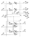
図3に、本発明のもう1つの実施形態を示す。破線320は、RO−1 327ないしRO−N 328によって表される単一方向信号線のNビット・バスの回路を示す。レシーバ(図ではREC)302ないし305は、単にNビット幅デバイス入出力バスの2つのレシーバである。入力信号であるRO−1 327およびRO−N 328は、レシーバ302および305に結合される。本発明のこの実施形態では、レシーバ302および305の出力が、オープン・コレクタ(図ではOC)ANDゲートであるゲート301および304に結合される。ゲート301および304の出力は、オープン・コレクタ・デバイスとして図示されているように、これらの出力とオープン・コレクタのゲートであるゲート307および313とのワイヤードORを容易にする。ゲート301および304またはゲート307および313の出力は、プロセッサ100などのプロセッサへの入力になる。
【0016】
破線321は、Nビット幅デバイス両方向入出力バスの2つのドライバおよび2つのレシーバを囲んでいる。D−1 325ないしD−N 326によって示されるプロセッサ(図示せず)からの出力信号線は、それぞれドライバ309および315に結合される。ドライバ309および315は、ドライバ・イネーブル信号線−DR 311によってゲーティングされる。ドライバ・イネーブル−DR 311がロウの時には、ドライバ309および315がイネーブルされ、ゲート307および313がディスエーブルされる。この条件の下で、信号線D/R−1 329ないしD/R−N 330によって示される両方向バスは、ドライブ・モードになる。ドライバ・イネーブル−DR 311がハイの時には、ドライバ309および315がディスエーブルされ、+EN 306もロウの場合にはゲート307および313がイネーブルされる。+EN 306がハイの場合には、ゲート307および313がディスエーブルされ、ゲート301および304がイネーブルされて、2つの別々のバスでの単一方向バス動作が可能になる。
【0017】
図3の回路は、プロセッサ側で単一方向であり、配線されたデバイス出力構造側で単一方向または両方向のいずれかであるバス構造の多数の可能な実施形態の1つの例にすぎない。本発明のこの実施形態では、プロセッサ入力バス信号線であるR−1 323ないしR−N 324が、Nビット幅プロセッサ入力バスの2つの信号線の例である。同様に、プロセッサ出力バス信号線であるD−1 325ないしD−N 326は、Nビット幅プロセッサ出力バスの2つの信号線である。これらの2つの単一方向バスおよび+EN 306は、基本マイクロプロセッサ・チップ構造内に設計される。ゲート301、304、307、および313によって示されるバス・ゲーティング・ネットワークの例は、両方向または単一方向のいずれかのデバイス・バス構造の選択を可能にするために実施される。
【0018】
デバイス入出力性能が重要である応用例では、D/R−1 329ないしD/R−N 330によって例示される両方向バス信号線とRO−1 327ないしRO−N 328によって例示される単一方向バス信号線の両方が、2つの太線334および336によって例示される配線を使用して第1レベル・チップ・パッケージングを介してチップの外部に配線されるはずである。これに対応して、単一方向通信をサポートする入出力デバイスを、プリント回路カードを介してマイクロプロセッサ・チップに配線することができる。
【0019】
+EN 306ゲート信号線を、太線339によって示される配線接続およびゲート340によって適当なレベルにセットして、プロセッサ・チップ内部の単一方向通信をイネーブルする。+EN 306のハイ・レベルによって、ゲート307および313もディスエーブルされ、レシーバ308および314がプロセッサ単一方向入力バスから除去される。
【0020】
マイクロプロセッサ・チップが使用可能であるが、システムが入出力速度を必要としない応用例では、D/R−1 329などの両方向信号線だけが、第1レベル・チップ・パッケージングを介してチップの外部に配線されるはずである。+EN 306ゲーティング信号線は、太線339によって示される配線接続が第1レベル・パッケージングを介してグラウンドに接続されない時にプルアップ抵抗331によって適当なレベルに駆動して、ゲート301および304を介して例示のレシーバ302および305をディスエーブルすることができる。さらに、太線334および336によって例示される接続を省略することができる。両方向バス構造は、低コスト・チップ・パッケージおよびより単純なプリント回路ボード配線のためにイネーブルされる。
【0021】
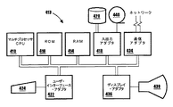
本発明を実施するための代表的なハードウェア環境を、図4に示す。図4は、本発明のマイクロプロセッサ・チップ設計などの中央処理装置(CPU)410と、システム・バス412を介して相互接続された複数の他のユニットとを有する、本発明によるデータ処理システム413の典型的なハードウェア構成を示す図である。データ処理システム413には、ランダム・アクセス・メモリ(RAM)414、読取専用メモリ(ROM)416、ディスク装置420およびテープ装置440などの周辺デバイスをシステム・バス412に接続する入出力アダプタ418、キーボード424またはタッチ・スクリーン・デバイス(図示せず)などの他のユーザ・インターフェース・デバイスをシステム・バス412に接続するユーザ・インターフェース・アダプタ422、データ処理システム413をデータ処理ネットワークに接続する通信アダプタ434、およびシステム・バス412をディスプレイ装置438に接続するディスプレイ・アダプタ436が含まれる。CPU410には、マイクロプロセッサ内に一般的に見られる回路、たとえば実行ユニット、バス・インターフェース・ユニット、算術演算装置などの回路を含む、図示されていない他の回路を含めることができる。CPU410は、単一の集積回路上に存在することもできる。本発明のバス構造を有するマイクロプロセッサ・チップを使用して、さまざまなシステム・ソリューションが可能になるはずである。
【図面の簡単な説明】
【図1】プロセッサがNビット両方向入出力バスを介して入出力デバイスに結合されるデータ処理システムを示す図である。
【図2】プロセッサがNビット単一方向入出力バスを介して入出力デバイスに結合されるデータ処理システムを示す図である。
【図3】単一方向バス構造または両方向バス構造のいずれかを選択するためのゲーティングを示す、本発明の一実施形態の回路実施形態を示す図である。
【図4】本発明に従って構成されたデータ処理システムを示す図である。
【符号の説明】
301 ゲート
302 レシーバ
304 ゲート
305 レシーバ
306 +EN
307 ゲート
308 レシーバ
309 ドライバ
311 −DR
313 ゲート
314 レシーバ
315 ドライバ
323 R−1
324 R−N
325 D−1
326 D−N
327 RO−1
328 RO−N
329 D/R−1
330 D/R−N
331 プルアップ抵抗[0001]
TECHNICAL FIELD OF THE INVENTION
The present invention relates generally to data processing systems, and more particularly, to input / output communication between a microprocessor and external system components.
[0002]
[Prior art]
Microprocessor chips (integrated circuits) have increased in complexity and more and more functions of the computer system have been integrated into the microprocessor chip. However, the performance of a chip depends on the flow of information, instructions, and data. As processor speeds increase, it becomes necessary to provide data and instructions to the processor at higher speeds. Memory is one of the increasing system requirements for bandwidth in communicating with microprocessor chips. Improvements in memory access speed have always led to increased costs. Over the years, memory has been partitioned into performance factors. A cache memory is a high speed memory that is loaded with information most accessed by a microprocessor. Cache memory is the fastest, and in high performance systems it is usually located on a microprocessor chip. A cache memory is typically a static RAM with the fastest access, the highest power, the highest cost, and the largest area per bit, of all the memory on a chip. As the memory bandwidth, and thus the cache size, increases with processor speed, some high-speed memory must be located off the microprocessor chip. Including all the required high-speed memory on a single chip causes an increase in chip size, thus lowering yield and increasing cost beyond acceptable limits for a given design.
[0003]
Some microprocessor designs use a bidirectional bus on the input / output signal lines as a way to reduce the number of input / output drivers and pins in a given design. Since bidirectional buses typically cannot simultaneously read and write, many applications requiring high I / O bandwidth can slow down the system. One solution to this problem is to increase the number of inputs and outputs and create separate unidirectional buses for the input and output signal lines, thus doubling the bandwidth. Unidirectional I / O buses increase chip cost by increasing the number of I / Os that must exit the microprocessor chip and be connected to second-level packaging. More I / O can increase the cost of the system board as well as the wiring complexity of systems that use the microprocessor chip.
[0004]
If the system requires performance, it is usually appropriate to pay a high cost to achieve high performance. However, it is often desirable to use a given chip architecture and design for multiple system level products. In this case, we do not want to pay for performance if we cannot recover due to increased sales or revenue of the system. However, it would be advantageous to use the volume of the entire system to reduce the overall manufacturing cost by achieving an economic scale by manufacturing more units of a particular microprocessor chip design.
[0005]
[Problems to be solved by the invention]
The present invention provides a solution to this problem by an alternative design of the input / output structure of the microprocessor chip.
[0006]
[Means for Solving the Problems]
The present invention discloses a microprocessor bus structure that can be optionally configured as a high performance unidirectional bus or a low performance bidirectional bus. Microprocessor chips are designed with an internal processor unidirectional I / O bus. These buses are coupled to selectively controlled device bidirectional input / output buses and optionally wired device unidirectional input buses. In one mode of operation, the device unidirectional input bus is routed externally via first level packaging. A binary unidirectional enable signal line is also routed at this time that disables the receiver of the device bidirectional input / output bus and allows the receiver of the device unidirectional input bus to be coupled to the processor unidirectional input bus. A binary bi-directional mode control signal line is also routed to enable the driver in the device bi-directional bus. The microprocessor chip has separate unidirectional buses for input and output wired from the processor to external devices via first level package wiring and printed circuit board interconnects. In another mode of operation, the device unidirectional input bus is not routed external to the chip, the binary unidirectional enable signal line is not selected, and the unidirectional receiver is gated off. A device bidirectional I / O bus is coupled to the processor unidirectional I / O bus. The binary bi-directional mode control signal line remains under the control of the processor, which allows the driver or receiver of the device bi-directional input / output bus to be selectively enabled.
[0007]
The foregoing has outlined rather broadly the features and technical advantages of the present invention in order that the detailed description of the invention that follows may be better understood. Additional features and advantages of the invention will be described hereinafter which form the subject of the claims of the invention.
[0008]
BEST MODE FOR CARRYING OUT THE INVENTION
In the following description, numerous specific details are set forth, such as specific word or byte lengths, to provide a thorough understanding of the present invention. However, it will be apparent to one skilled in the art that the present invention may be practiced without such specific details. In other instances, well-known circuits have been shown in block diagram form in order not to obscure the present invention in unnecessary detail. For the most part, details regarding timing considerations and the like are set forth in detail only if such details are not necessary to obtain a complete understanding of the invention and are within the skill of those having ordinary skill in the relevant art. Was omitted.
[0009]
Referring now to the drawings wherein like elements are not necessarily drawn to scale, similar or similar elements are designated with the same reference numerals throughout the drawings.
[0010]
FIG. 1 is a diagram showing a data processing system including a
[0011]
FIG. 2 shows the same system elements coupled by two
[0012]
A problem with bus speed and bus contention in the exemplary system configuration is communication between the processor and external memory. The higher the processing speed, the faster the processor must execute instructions and the faster the transmission and storage of data or results generated by processing functions. However, as the amount of memory required to support a given system architecture increases with the speed of processor instruction execution, sufficient fast (cache) memory is placed on the chip to allow for external storage away from the processor chip. It is not always possible to completely eliminate the need for high-speed communication to memory.
[0013]
The performance of input / output signal lines exiting from the chip to external devices coupled to the chip is degraded by the capacitance, inductance, and length of the input / output signal lines as the speed of communication on these lines increases. Also, the number of input / output signal lines emanating from the chip increases the cost of the first-level package, which is a structure for housing the chip and the conductor connecting the chip to the outside. The first level package or integrated circuit package contains conductors used to couple to the next level wiring structure, either a module or a printed circuit board or card. It is also possible for an integrated circuit to have a "chip-on-board" or "chip-on-module" circuit package that is wired directly to a wiring structure that couples it to other chips or components.
[0014]
In either a chip-on-board or a chip-on-module, depending on the number of inputs and outputs of the integrated circuit or chip, the complexity of the circuit board on which the integrated circuit or processor chip is routed to other system devices It will increase. It is not uncommon for modern processors to have very wide input / output connection buses to facilitate high performance operation. These wide I / O buses further complicate I / O and wiring issues when a unidirectional bus is used.
[0015]
FIG. 3 shows another embodiment of the present invention. Dashed line 320 shows the circuitry of the unidirectional signal line N-bit bus represented by RO-1 327 through RO-
[0016]
Dashed
[0017]
The circuit of FIG. 3 is only one example of many possible embodiments of a bus structure that is unidirectional on the processor side and either unidirectional or bidirectional on the wired device output structure side. In this embodiment of the invention, the processor input bus signal lines, R-1 323 through
[0018]
In applications where device input / output performance is important, bidirectional bus signal lines exemplified by D / R-1 329 through D /
[0019]
The +
[0020]
In applications where a microprocessor chip is available but the system does not require I / O speed, only bi-directional signal lines, such as D / R-1 329, may be chipped via first level chip packaging. It should be wired outside. The +
[0021]
FIG. 4 shows a typical hardware environment for implementing the present invention. FIG. 4 shows a data processing system 413 according to the present invention having a central processing unit (CPU) 410, such as a microprocessor chip design of the present invention, and a plurality of other units interconnected via a system bus 412. 3 is a diagram showing a typical hardware configuration of FIG. The data processing system 413 includes a random access memory (RAM) 414, a read-only memory (ROM) 416, an input /
[Brief description of the drawings]
FIG. 1 illustrates a data processing system in which a processor is coupled to an input / output device via an N-bit bidirectional input / output bus.
FIG. 2 illustrates a data processing system in which a processor is coupled to an input / output device via an N-bit unidirectional input / output bus.
FIG. 3 illustrates a circuit embodiment of one embodiment of the present invention, showing gating to select either a unidirectional bus structure or a bidirectional bus structure.
FIG. 4 is a diagram showing a data processing system configured according to the present invention.
[Explanation of symbols]
301 Gate 302 Receiver 304
313
324 RN
325 D-1
326 DN
327 RO-1
328 RO-N
329 D / R-1
330 D / RN
331 pull-up resistor
Claims (1)
プロセッサ単一方向出力バスと、
レシーバの第1組および第1ゲーティング・ネットワークを介して前記プロセッサ単一方向入力バスに選択的に結合されるデバイス単一方向入力バスであって、前記単一方向デバイス入力バスが、前記レシーバの第1組の信号線を介して前記プロセッサ単一方向入力バスの対応する信号線に選択的に結合される、デバイス単一方向入力バスと、
レシーバの第2組、ドライバの第1組、および第2ゲーティング・ネットワークを介して前記プロセッサ単一方向出力バスおよび前記プロセッサ単一方向入力バスに選択的に結合されるデバイス両方向入出力バスであって、前記デバイス両方向入出力バスが、前記レシーバの第2組の信号線を介して前記プロセッサ単一方向入力バスの対応する信号線に選択的に結合されるとともに、前記ドライバの第1組の信号線を介して前記プロセッサ単一方向出力バスの対応する信号線に選択的に結合される、デバイス両方向入出力バスと、
前記第2ゲーティング・ネットワークを介して、(1)第1状態である時に前記ドライバの第1組をイネーブルし、前記レシーバの第2組をディスエーブルし、(2)第2状態である時に前記ドライバの第1組をディスエーブルし、前記レシーバの第2組をイネーブルするように動作可能なモード選択信号線と、
前記第1ゲーティング・ネットワークを介して、(1)第1状態である時に前記レシーバの第1組をイネーブルし、前記レシーバの第2組をディスエーブルし、(2)第2状態である時に前記レシーバの第1組をディスエーブルし、前記レシーバの第2組をイネーブルするように動作可能なバス・ゲーティング信号線とを備え、
前記プロセッサ単一方向入力バスおよび前記プロセッサ単一方向出力バスでの同時的な単一方向バス動作を可能にするために前記デバイス単一方向入力バスおよび前記デバイス両方向入出力バスを同時に使用する時には、前記モード選択信号線および前記バス・ゲーティング信号線の各々がそれぞれの前記第1状態にセットされ、
前記プロセッサ単一方向入力バスおよび前記プロセッサ単一方向出力バスでの順次的な単一方向バス動作を可能にするために前記デバイス両方向入出力バスのみを使用する時には、前記バス・ゲーティング信号線が前記第2状態にセットされるとともに、当該単一方向バス動作がドライブ動作またはレシーブ動作のいずれであるかに応じて、前記モード選択信号線が前記第1状態または前記第2状態にセットされるようにしたことを特徴とする、プロセッサ・バス構造。A processor unidirectional input bus;
A processor unidirectional output bus;
A first set and a first gating device single side MukoIri force bus network via a Ru are selectively coupled to the processor unidirectional input bus of the receiver, the unidirectional device input bus, said through the first set of signal lines of the receiver is selectively coupled to a corresponding signal line of the processor unidirectional input bus, and the device single side MukoIri force bus,
A second set of receivers, a first set of drivers, and a device bidirectional I / O bus selectively coupled to the processor unidirectional output bus and the processor unidirectional input bus via a second gating network. Wherein the device bidirectional input / output bus is selectively coupled to a corresponding signal line of the processor unidirectional input bus via a second set of signal lines of the receiver, and the first set of drivers is provided. A device bidirectional input / output bus, selectively coupled to corresponding signal lines of the processor unidirectional output bus via signal lines of :
Via the second gating network: (1) enabling the first set of drivers when in the first state, disabling the second set of receivers; and (2) when in the second state. A mode select signal line operable to disable the first set of drivers and enable the second set of receivers;
Via the first gating network: (1) enabling the first set of receivers when in the first state, disabling the second set of receivers, and (2) when in the second state. Bus gating signal lines operable to disable the first set of receivers and to enable the second set of receivers ;
When using the device unidirectional input bus and the device bidirectional I / O bus simultaneously to enable simultaneous unidirectional bus operation on the processor unidirectional input bus and the processor unidirectional output bus , Each of the mode selection signal line and the bus gating signal line is set to a respective first state,
The bus gating signal line is used when only the device bidirectional I / O bus is used to enable sequential unidirectional bus operation on the processor unidirectional input bus and the processor unidirectional output bus. Is set to the second state, and the mode selection signal line is set to the first state or the second state depending on whether the unidirectional bus operation is a drive operation or a receive operation. A processor bus structure , characterized in that:
Applications Claiming Priority (2)
| Application Number | Priority Date | Filing Date | Title |
|---|---|---|---|
| US09/422368 | 1999-10-21 | ||
| US09/422,368 US6457089B1 (en) | 1999-10-21 | 1999-10-21 | Microprocessor bus structure |
Publications (2)
| Publication Number | Publication Date |
|---|---|
| JP2001175370A JP2001175370A (en) | 2001-06-29 |
| JP3574061B2 true JP3574061B2 (en) | 2004-10-06 |
Family
ID=23674599
Family Applications (1)
| Application Number | Title | Priority Date | Filing Date |
|---|---|---|---|
| JP2000311665A Expired - Fee Related JP3574061B2 (en) | 1999-10-21 | 2000-10-12 | Processor bus structure |
Country Status (3)
| Country | Link |
|---|---|
| US (1) | US6457089B1 (en) |
| JP (1) | JP3574061B2 (en) |
| IL (1) | IL137632A0 (en) |
Families Citing this family (7)
| Publication number | Priority date | Publication date | Assignee | Title |
|---|---|---|---|---|
| US6725304B2 (en) * | 2000-12-19 | 2004-04-20 | International Business Machines Corporation | Apparatus for connecting circuit modules |
| US7400670B2 (en) | 2004-01-28 | 2008-07-15 | Rambus, Inc. | Periodic calibration for communication channels by drift tracking |
| US7158536B2 (en) * | 2004-01-28 | 2007-01-02 | Rambus Inc. | Adaptive-allocation of I/O bandwidth using a configurable interconnect topology |
| US7095789B2 (en) | 2004-01-28 | 2006-08-22 | Rambus, Inc. | Communication channel calibration for drift conditions |
| US8422568B2 (en) | 2004-01-28 | 2013-04-16 | Rambus Inc. | Communication channel calibration for drift conditions |
| US6961862B2 (en) | 2004-03-17 | 2005-11-01 | Rambus, Inc. | Drift tracking feedback for communication channels |
| US8543753B2 (en) * | 2011-04-06 | 2013-09-24 | International Business Machines Corporation | Multi-use physical architecture |
Family Cites Families (2)
| Publication number | Priority date | Publication date | Assignee | Title |
|---|---|---|---|---|
| US4261034A (en) * | 1979-07-02 | 1981-04-07 | Computer Automation, Inc. | Remote distributed interrupt control for computer peripherals |
| US6034545A (en) * | 1998-01-30 | 2000-03-07 | Arm Limited | Macrocell for data processing circuit |
-
1999
- 1999-10-21 US US09/422,368 patent/US6457089B1/en not_active Expired - Fee Related
-
2000
- 2000-08-01 IL IL13763200A patent/IL137632A0/en not_active IP Right Cessation
- 2000-10-12 JP JP2000311665A patent/JP3574061B2/en not_active Expired - Fee Related
Also Published As
| Publication number | Publication date |
|---|---|
| IL137632A0 (en) | 2001-10-31 |
| JP2001175370A (en) | 2001-06-29 |
| US6457089B1 (en) | 2002-09-24 |
Similar Documents
| Publication | Publication Date | Title |
|---|---|---|
| KR100288038B1 (en) | Pipeline semiconductor device suitable for ultra-large scale integration | |
| US7680968B2 (en) | Switch/network adapter port incorporating shared memory resources selectively accessible by a direct execution logic element and one or more dense logic devices in a fully buffered dual in-line memory module format (FB-DIMM) | |
| US8572297B2 (en) | Programmable system-on-chip hub | |
| US5526497A (en) | System having switch that provides capacitive load isolation | |
| US7424552B2 (en) | Switch/network adapter port incorporating shared memory resources selectively accessible by a direct execution logic element and one or more dense logic devices | |
| US4755937A (en) | Method and apparatus for high bandwidth shared memory | |
| US20020103988A1 (en) | Microprocessor with integrated interfaces to system memory and multiplexed input/output bus | |
| US6883053B2 (en) | Data transfer control circuit with interrupt status register | |
| US5970236A (en) | Circuit for selectively performing data format conversion | |
| JPS6327738B2 (en) | ||
| CA1129110A (en) | Apparatus and method for providing byte and word compatible information transfers | |
| JPH05204820A (en) | Microcessor, processing system and bus interface | |
| US5740385A (en) | Low load host/PCI bus bridge | |
| US5838995A (en) | System and method for high frequency operation of I/O bus | |
| JP3574061B2 (en) | Processor bus structure | |
| JPH08314590A (en) | Data-processing system with multifunction scalable parallel input/output port | |
| US6580288B1 (en) | Multi-property microprocessor with no additional logic overhead to shared pins | |
| US6898659B2 (en) | Interface device having variable data transfer mode and operation method thereof | |
| GB1595471A (en) | Computer system | |
| US4494186A (en) | Automatic data steering and data formatting mechanism | |
| US6631444B2 (en) | Cache architecture for pipelined operation with on-die processor | |
| US6311247B1 (en) | System for bridging a system bus with multiple PCI buses | |
| US6034545A (en) | Macrocell for data processing circuit | |
| US6064254A (en) | High speed integrated circuit interconnection having proximally located active converter | |
| US6377581B1 (en) | Optimized CPU-memory high bandwidth multibus structure simultaneously supporting design reusable blocks |
Legal Events
| Date | Code | Title | Description |
|---|---|---|---|
| A131 | Notification of reasons for refusal |
Free format text: JAPANESE INTERMEDIATE CODE: A131 Effective date: 20040127 |
|
| A521 | Request for written amendment filed |
Free format text: JAPANESE INTERMEDIATE CODE: A523 Effective date: 20040312 |
|
| TRDD | Decision of grant or rejection written | ||
| A01 | Written decision to grant a patent or to grant a registration (utility model) |
Free format text: JAPANESE INTERMEDIATE CODE: A01 Effective date: 20040615 |
|
| A61 | First payment of annual fees (during grant procedure) |
Free format text: JAPANESE INTERMEDIATE CODE: A61 Effective date: 20040630 |
|
| R150 | Certificate of patent or registration of utility model |
Free format text: JAPANESE INTERMEDIATE CODE: R150 |
|
| FPAY | Renewal fee payment (event date is renewal date of database) |
Free format text: PAYMENT UNTIL: 20070709 Year of fee payment: 3 |
|
| FPAY | Renewal fee payment (event date is renewal date of database) |
Free format text: PAYMENT UNTIL: 20080709 Year of fee payment: 4 |
|
| LAPS | Cancellation because of no payment of annual fees |