JP3570397B2 - Dielectric filter, dielectric duplexer and communication device - Google Patents
Dielectric filter, dielectric duplexer and communication device Download PDFInfo
- Publication number
- JP3570397B2 JP3570397B2 JP2001186525A JP2001186525A JP3570397B2 JP 3570397 B2 JP3570397 B2 JP 3570397B2 JP 2001186525 A JP2001186525 A JP 2001186525A JP 2001186525 A JP2001186525 A JP 2001186525A JP 3570397 B2 JP3570397 B2 JP 3570397B2
- Authority
- JP
- Japan
- Prior art keywords
- inner conductor
- conductor forming
- dielectric
- short
- holes
- Prior art date
- Legal status (The legal status is an assumption and is not a legal conclusion. Google has not performed a legal analysis and makes no representation as to the accuracy of the status listed.)
- Expired - Lifetime
Links
Images


Classifications
-
- H—ELECTRICITY
- H01—ELECTRIC ELEMENTS
- H01P—WAVEGUIDES; RESONATORS, LINES, OR OTHER DEVICES OF THE WAVEGUIDE TYPE
- H01P1/00—Auxiliary devices
- H01P1/20—Frequency-selective devices, e.g. filters
- H01P1/201—Filters for transverse electromagnetic waves
- H01P1/205—Comb or interdigital filters; Cascaded coaxial cavities
- H01P1/2056—Comb filters or interdigital filters with metallised resonator holes in a dielectric block
-
- H—ELECTRICITY
- H01—ELECTRIC ELEMENTS
- H01P—WAVEGUIDES; RESONATORS, LINES, OR OTHER DEVICES OF THE WAVEGUIDE TYPE
- H01P1/00—Auxiliary devices
- H01P1/20—Frequency-selective devices, e.g. filters
- H01P1/213—Frequency-selective devices, e.g. filters combining or separating two or more different frequencies
- H01P1/2136—Frequency-selective devices, e.g. filters combining or separating two or more different frequencies using comb or interdigital filters; using cascaded coaxial cavities
Landscapes
- Physics & Mathematics (AREA)
- Electromagnetism (AREA)
- Control Of Motors That Do Not Use Commutators (AREA)
Description
【0001】
【発明の属する技術分野】
この発明は、マイクロ波帯等で使用される誘電体フィルタ、誘電体デュプレクサおよびそれらを用いた通信装置に関するものである。
【0002】
【従来の技術】
単一の誘電体ブロック内に複数の内導体形成孔を配列することによって、隣接する共振器間を結合させた、誘電体同軸共振器による誘電体フィルタが、マイクロ波帯における通信装置等に用いられている。このような構造の誘電体フィルタにおいては、隣接する共振器間の結合が容量性結合の場合に、通過帯域の低域側に減衰極が生じ、隣接する共振器間の結合が誘導性結合の場合に、通過帯域の高域側に減衰極が生じる。
【0003】
そこで、従来は、特開平7−254806号公報に示されているように、内導体形成孔の途中に段差部を設けて、内導体形成孔の短絡端側と開放端側とで、隣接する内導体形成孔間の軸間隔によって誘導性結合または容量性結合させている。
【0004】
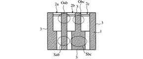
その例を図12および図13に示す。
図12において(A)は内導体形成孔の軸方向を見た上面図、(B)は各内導体形成孔の中心軸を通る面での断面図である。略直方体形状の誘電体ブロック1の内部には、内面に内導体を形成した、2a,2b,2cで示す内導体形成孔を設けている。誘電体ブロック1の外面には外導体3を形成している。図12に示す例では、内導体形成孔2aと2bについて、その開放端側の軸間隔を短絡端側の軸間隔より広くして、Oabで示す部分の容量性結合より、Sabで示す部分の誘導性結合を強くして、この内導体形成孔2a,2bによる2つの共振器間を誘導性結合させている。同様に内導体形成孔2bと2cとの間についても、その開放端側の軸間隔を短絡端側の軸間隔より広くして、Obcで示す部分の容量性結合より、Sbcで示す部分の誘導性結合を強くして、この内導体形成孔2b,2cによる2つの共振器間を誘導性結合させている。
【0005】
図13に示す例では、内導体形成孔2a,2bについて、短絡端側の軸間隔を開放端側の軸間隔より狭くして、Oab部分の容量性結合より、Sab部分の誘導性結合を増して、内導体形成孔2a,2bによる2つの共振器間を強く誘導性結合させている。また、内導体形成孔2bと2cとの間については、開放端側の軸間隔を短絡端側の軸間隔より狭くして、Sbc部分の誘導性結合より、Obc部分の容量性結合を増して、内導体形成孔2b,2cによる2つの共振器間を容量性結合させている。
【0006】
【発明が解決しようとする課題】
ところが、図12および図13に示したような、3段の共振器を構成した誘電体フィルタにおいては、1段目と2段目の共振器間の誘導性結合を強くするために、2段目の共振器の短絡端側を1段目の共振器に近づけると、その分、2段目の共振器の短絡端側は3段目の共振器の短絡端側から離れることになり、2段目と3段目の共振器間の誘導性結合が弱くなってしまう。1段目と2段目の共振器間、および2段目と3段目の共振器間における短絡端側の相互容量をどちらも大きくしようとして、短絡端側の内導体形成孔の内径を大きくすると、各共振器の自己インピーダンスが小さくなって、相対的に相互容量が小さくなることにより、誘導性結合を高める効果が相殺されてしまう。また、これとともに、内導体形成孔の短絡端側と開放端側との内径比(ステップ比)が小さくなるため、波長短縮率が小さくなって、必要な内導体形成孔の軸長が伸びて、大型化するという不都合が生じる。
【0007】
これらの理由から、隣接する3つの共振器で、1段目と2段目との間および2段目と3段目との間を共に誘導性結合するためには、その結合量に制限が生じていた。
【0008】
この発明の目的は、全体に大型化することなく、誘電体ブロック内の隣接する3つの誘電体共振器を共に強く誘導性結合し得るようにした誘電体フィルタ、誘電体デュプレクサおよびそれらを備えた通信装置を提供することにある。
【0009】
【課題を解決するための手段】
この発明は、略直方体形状の誘電体ブロック内に、当該誘電体ブロックの対向する第1面と第2面との間をそれぞれ貫通し、第1面を短絡端、第2面または第2面付近を開放端とする内導体を形成した複数の内導体形成孔を備え、前記誘電体ブロックの外面に外導体を形成した誘電体フィルタにおいて、前記複数の内導体形成孔のうち、少なくとも1つの内導体形成孔は、短絡端側の内導体形成孔を少なくとも2つの孔に分割する。
【0010】
この構造により、例えば中央の内導体形成孔と、その両隣の内導体形成孔の短絡端側の軸間隔を共に狭くして、1段目と2段目の共振器間および2段目と3段目の共振器間の誘導性結合を強め得るようにする。
【0011】
また、この発明は、上記分割位置を、内導体形成孔の長手方向の略中央部とする。これにより、誘導性結合の向上効果を高める。
【0012】
また、この発明は上記誘電体フィルタを用いて誘電体デュプレクサを構成する。
【0013】
また、この発明は上記誘電体フィルタまたは誘電体デュプレクサを用いて通信装置を構成する。
【0014】
【発明の実施の形態】
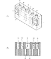
第1の実施形態に係る誘電体フィルタの構成を図1に示す。
図1の(A)は実装基板への実装面を図における左手前の面に向けて立てた状態の誘電体フィルタの斜視図である。(B)は(A)における複数の内導体の軸を通る面での断面図である。1は略直方体形状の誘電体ブロックである。この誘電体ブロック1の内部には、その第1面(図における下面)から第2面(図における上面)を貫通する内導体形成孔2a,2b,2cを設けている。これらの内導体形成孔の内面には内導体4a,4b,4cを形成している。誘電体ブロック1の外面(六面)には外導体3を形成している。内導体4a,4b,4cの一端は第1面(下面)において外導体3に導通(短絡)させている。内導体形成孔の第2面の開口部付近には内導体非形成部gを設けていて、この部分を内導体の開放端としている。誘電体ブロック1の外面には、内導体4a,4cの開放端付近との間に静電容量が生じる入出力電極6,7を、外導体3から絶縁状態に形成している。
【0015】
内導体形成孔2bの開放端側(内導体の開放端寄りの側)の断面形状は、隣接する内導体形成孔2a,2cの方向にそれぞれ延びる長円形状としている。また、この内導体形成孔2bの短絡端側(内導体の短絡端寄りの側)は、2つの孔2b′,2b″に分割している。この2つの孔2b′,2b″は、それぞれが隣接する内導体形成孔2a,2cの短絡端側に近づくように配置している。
【0016】
内導体形成孔2a,2cは、開放端側の内径を短絡端側の内径より大きくし、且つ、短絡端側を内導体形成孔2bの短絡端側(2b′,2b″側)に近づくように配置している。
【0017】
このように、中央の内導体形成孔2bの短絡端側2b′,2b″と、隣接する内導体形成孔2a,2cの短絡端側との間隔を、開放端側に比べて相対的に狭めたことにより、Sab,Sbc部分の誘導性結合が、Oab,Obc部分の容量性結合より強くなって、1段目と2段目の共振器間、および2段目と3段目の共振器間が共に強く誘導性結合する。
【0018】
なお、内導体形成孔2bの分割位置は任意であるが、内導体形成孔の長手方向の略中央部に定めるのが好ましい。この構造により、磁界強度の強い領域で、隣接する内導体形成孔の内導体に近接させることができる。その結果、隣接する内導体形成孔による共振器との間で取得可能な結合量を最大にすることができ、設計上の自由度が高くなる。また、開放端側の断面を短絡端側の断面より太くすることによる、すなわちステップ構造とすることによる、内導体形成孔の軸長短縮効果を高めることもできる。
【0019】
次に、第2の実施形態に係る誘電体フィルタの構成を図2に示す。
図1に示した誘電体フィルタとの違いは内導体形成孔の形状である。図2に示す例では、内導体形成孔2bの短絡端側を2b′,2b″で示すように2つに分割している点、および隣接する内導体形成孔の短絡端側の軸間隔を開放端側の軸間隔より狭くしている点で同じである。但し、内導体形成孔2a,2cの短絡端側の横断幅が開放端側の横断幅より外側に広がらないようにしている。また、内導体形成孔2bの短絡端側の孔2b′,2b″が、2bの開放端側の長軸方向の横断幅より外側に広がらない範囲に収めている。
【0020】
このような構造であっても、1段目と2段目の共振器間および2段目と3段目の共振器間の誘導性結合を容量性結合より相対的に高めて、共に強く誘導性結合させることができる。
【0021】
次に、第3の実施形態に係る誘電体フィルタの構造を図3に示す。図2に示した誘電体フィルタと異なるのは、内導体形成孔の形状である。図2に示した例では、中央の内導体形成孔2bの短絡端側2b′,2b″の内径を等しくしたが、この図3に示す例では、2b″を2b′より太くしている。この構造により、図2に示した誘電体フィルタに比べて、Sbc部分の誘導性結合がより強くなるため、内導体4bによる2段目の共振器と内導体4cによる3段目の共振器間の誘導性結合がより強くなる。
【0022】
図4は第4の実施形態に係る誘電体フィルタの内導体形成孔の軸方向を見た図である。第1〜第3の実施形態では、分割した短絡端側の内導体形成孔の断面形状を円形にしたが、これを図4のように半円形状としてもよい。また、その他に矩形や多角形等としてもよい。
【0023】
次に、第5の実施形態に係る誘電体フィルタの構造を図5に示す。内導体形成孔2bの開放端側の断面形状は、隣接する内導体形成孔2a,2cの方向にそれぞれ延びる長円形状としている。また、この内導体形成孔2bの短絡端側は、2つの孔2b′,2b″に分割し、それぞれが隣接する内導体形成孔2a,2cの短絡端側に近づくように配置している。この点は図1に示した誘電体フィルタと同様である。但し、図1に示した例では、内導体形成孔2a,2cを、その開放端側の内径を短絡端側の内径より大きくし、且つ、短絡端側を内導体形成孔2bの短絡端側(2b′,2b″側)に近づくように配置したが、この図5に示す例では、内導体形成孔2a,2cの内径を一定にしている。このような構造であっても、内導体4aによる1段目の共振器と内導体2bによる2段目の共振器間を強く誘導性結合させ、且つ、内導体4bによる2段目の共振器と内導体4cによる3段目の共振器間を強く誘導性結合させることができる。
【0024】
次に、第6の実施形態に係る誘電体フィルタの斜視図を図6に示す。図1に示した例では、誘電体ブロック1の外面(六面)に外導体3を形成し、内導体形成孔の一方の開口付近に内導体非形成部による開放端を形成したが、この図6に示す例では、誘電体ブロック1の図における上面に外導体を形成せず、その面を開放面とし、他の五面に外導体3を形成している。このようなタイプの誘電体フィルタにおいても、内導体形成孔の短絡端側を分割し、それに隣接する内導体形成孔との間で強く誘導性結合させることができる。
【0025】
次に、第7の実施形態に係る誘電体フィルタの斜視図を図7に示す。図6に示した誘電体フィルタと異なるのは、誘電体ブロック1の開放面に、内導体から連続する結合用電極5a,5b,5cを形成したことと、結合用電極5a,5cとの間で静電容量を生じさせる入出力電極6,7を形成したことである。このようなタイプの誘電体フィルタにおいても、第1〜第6の実施形態の場合と同様の効果が得られる。
【0026】
次に、第8の実施形態に係る誘電体フィルタの構成を図8に示す。図8の(A)は外観斜視図、(B)は各内導体形成孔を軸方向に通る面での断面図である。この例では、内導体形成孔2a〜2dによる4段の共振器によりフィルタを構成している。内導体形成孔2b,2cは、それぞれの短絡端側を2つに分割し、短絡端側の隣接する軸間隔が狭くなるように形成している。その他の構成は、共振器の段数が1つ多いという点を除いて図1に示した誘電体フィルタと同様である。このようにして、1段目と2段目、2段目と3段目、3段目と4段目の各共振器間をすべて強く誘導性結合させることができる。これにより、広帯域の帯域通過特性を示す誘電体フィルタが得られる。
【0027】
次に、第9の実施形態に係る誘電体フィルタの構成を図9に示す。(A)は斜視図、(B)は各内導体形成孔を通る面での断面図である。この例では、2a〜2eで示す5つの内導体形成孔による5段の共振器を備えた誘電体フィルタとしている。内導体形成孔2a,2bによる共振器間は、内導体形成孔2a,2bの開放端側の軸間隔を短絡端側の軸間隔より相対的に狭めて、両者を容量性結合させている。同様にして、内導体形成孔2d,2eによる共振器間も容量性結合させている。内導体形成孔2cの短絡端は、2c′,2c″に分割していて、この分割した内導体形成孔2c′,2c″と内導体形成孔2b,2dの短絡端側とを相対的に近接させることによって、2段目と3段目の共振器間および3段目と4段目の共振器間を共に誘導性結合させている。
【0028】
次に、第10の実施形態に係る誘電体デュプレクサの構成を図10を参照して説明する。
図10は実装基板に対する実装面側から見た平面図である。略直方体形状の単一の誘電体ブロック1の内部には、2a〜2fで示す内導体形成孔を設けている。これらの内導体形成孔2a〜2fの内面には内導体を形成している。但し、これらの内導体形成孔の一方の開口付近には、内導体非形成部を設けていて、その部分で内導体を開放させている。また、誘電体ブロック1の内部には、内面に内導体を形成した励振孔9を設けている。誘電体ブロック1の外面(六面)には外導体3を形成している。また、誘電体ブロック1の外面には、外導体3から絶縁状態に入出力電極6,7,8を形成している。入出力電極6,7は内導体形成孔2a,2fの内導体の開放端付近との間でそれぞれ容量性結合する。また、入出力電極8は励振孔9の内面の内導体に導通させていて、励振孔9の内導体を内導体形成孔2c,2dによる2つの共振器にそれぞれインターディジタル的に結合させている。
【0029】
内導体形成孔2bの開放端側(内導体の開放端寄りの側)の断面形状は、隣接する内導体形成孔2a,2cの方向にそれぞれ延びる長円形状としている。また、この内導体形成孔2bの短絡端側(内導体の短絡端寄りの側)は、2つの孔2b′,2b″に分割している。この2つの孔2b′,2b″は、それぞれが隣接する内導体形成孔2a,2cの短絡端側に近づくように配置している。
【0030】
内導体形成孔2a,2cは、開放端側の内径を短絡端側の内径より大きくし、且つ、短絡端側を内導体形成孔2bの短絡端側(2b′,2b″側)に近づくように配置している。
【0031】
このように、中央の内導体形成孔2bの短絡端側2b′,2b″と、隣接する内導体形成孔2a,2cの短絡端側との間隔を、開放端側に比べて相対的に狭めたことにより、内導体形成孔2aによる1段目の共振器と、内導体形成孔2bによる2段目の共振器間、および2段目の共振器と内導体形成孔2cによる3段目の共振器間が共に強く誘導性結合する。
【0032】
このような構造により、内導体形成孔2a〜2cによる3段の共振器で送信フィルタを、内導体形成孔2d〜2fによる3段の共振器で受信フィルタを、それぞれ構成している。内導体形成孔2a〜2cによる3段の共振器は、上述したとおり、1段目と2段目の共振器間および2段目と3段目の共振器間がそれぞれ誘導性結合するため、送信フィルタの高域側に減衰極が生じる。また、内導体形成孔2d〜2fによる3段の共振器は、隣接する内導体形成孔の開放端側の軸間隔が短絡端側より相対的に狭いため、それぞれ容量性結合し、受信フィルタの低域側に減衰極が生じる。これらの減衰極によって送信帯域と受信帯域の境界部分の減衰量を大きく確保する。
【0033】
次に、第11の実施形態に係る通信装置の構成を図11に示す。
ここで、デュプレクサは、送信フィルタと受信フィルタとから成り、図10に示した構造の誘電体デュプレクサである。このデュプレクサの送信信号入力ポートには送信回路を接続し、受信信号出力ポートには受信回路を接続し、さらにアンテナポートにはアンテナを接続している。また、送信回路における出力部および受信回路における入力部には、それぞれ帯域通過フィルタを備えていて、これらのフィルタは、図1〜図9に示した構造の誘電体フィルタである。
【0034】
このようにして、小型で且つ所定の特性を有する誘電体フィルタまたは誘電体デュプレクサを用いることにより、全体に小型軽量化した通信装置を得る。
【0035】
【発明の効果】
この発明によれば、略直方体形状の誘電体ブロック内に、それぞれの内面に内導体を形成した複数の内導体形成孔を配列した誘電体フィルタにおいて、複数の内導体形成孔のうち、少なくとも1つの内導体形成孔の短絡端側を少なくとも2つの孔に分割したことにより、設計上の自由度が飛躍的に高まる。例えば中央の内導体形成孔と、それに隣接する両隣の内導体形成孔の短絡端側の軸間隔を共に狭くすることができる。この構造により、中央の内導体形成孔による共振器と、それに隣接する両隣の内導体形成孔による共振器との間を共に強く誘導性結合させ、例えば広帯域の通過特性を容易に得ることができる。
【0036】
また、この発明によれば、上記分割位置を、内導体形成孔の長手方向の略中央部としたことにより、磁界強度の強い領域で、隣接する内導体形成孔の内導体に近接させることができ、その結果、隣接する内導体形成孔による共振器との間で取得可能な結合量を最大にすることができ、設計上の自由度が高くなる。それと同時に、開放端側の断面を短絡端側の断面より太くすることによる、すなわちステップ構造とすることによる、内導体形成孔の軸長短縮効果を高めることもできる。
【0037】
また、この発明によれば、順に隣接する共振器間を連続して強く誘導性結合させることができ、所定のフィルタ特性を示す小型の誘電体デュプレクサが構成できる。
【0038】
また、この発明によれば、上記誘電体フィルタまたは誘電体デュプレクサを用いた、優れた通信性能を備えた小型の通信装置が得られる。
【図面の簡単な説明】
【図1】第1の実施形態に係る誘電体フィルタの構成を示す図
【図2】第2の実施形態に係る誘電体フィルタの構成を示す図
【図3】第3の実施形態に係る誘電体フィルタの構成を示す図
【図4】第4の実施形態に係る誘電体フィルタの構成を示す図
【図5】第5の実施形態に係る誘電体フィルタの構成を示す図
【図6】第6の実施形態に係る誘電体フィルタの構成を示す図
【図7】第7の実施形態に係る誘電体フィルタの構成を示す図
【図8】第8の実施形態に係る誘電体フィルタの構成を示す図
【図9】第9の実施形態に係る誘電体フィルタの構成を示す図
【図10】第10の実施形態に係る誘電体デュプレクサの構成を示す図
【図11】第11の実施形態に係る通信装置の構成を示すブロック図
【図12】従来の誘電体フィルタの構成を示す図
【図13】従来の誘電体フィルタの構成を示す図
【符号の説明】
1−誘電体ブロック
2−内導体形成孔
3−外導体
4−内導体
5−結合用電極
6,7,8−入出力電極
9−励振孔
g−内導体非形成部[0001]
TECHNICAL FIELD OF THE INVENTION
The present invention relates to a dielectric filter and a dielectric duplexer used in a microwave band or the like and a communication device using the same.
[0002]
[Prior art]
By arranging a plurality of inner conductor forming holes in a single dielectric block, a dielectric filter with a dielectric coaxial resonator, which connects adjacent resonators, is used for communication devices in the microwave band. Have been. In a dielectric filter having such a structure, when coupling between adjacent resonators is capacitive coupling, an attenuation pole is generated on the lower side of the pass band, and coupling between adjacent resonators is inductive coupling. In this case, an attenuation pole is generated on the high band side of the pass band.
[0003]
Therefore, conventionally, as shown in Japanese Patent Laid-Open No. 7-254806, a step is provided in the middle of the inner conductor forming hole, and the inner conductor forming hole is adjacent to the short-circuit end side and the open end side. Inductive coupling or capacitive coupling is performed by the axial interval between the inner conductor forming holes.
[0004]
Examples are shown in FIGS.
In FIG. 12, (A) is a top view of the inner conductor forming hole as viewed in the axial direction, and (B) is a cross-sectional view of a plane passing through the center axis of each inner conductor forming hole. Inside the dielectric block 1 having a substantially rectangular parallelepiped shape, inner conductor forming holes indicated by 2a, 2b and 2c having inner conductors formed on the inner surface are provided. An
[0005]
In the example shown in FIG. 13, in the inner
[0006]
[Problems to be solved by the invention]
However, in a dielectric filter having a three-stage resonator as shown in FIG. 12 and FIG. 13, the two-stage resonator is required to strengthen the inductive coupling between the first and second resonators. When the short-circuit end of the second resonator is brought closer to the first-stage resonator, the short-circuit end of the second-stage resonator is further away from the short-circuit end of the third-stage resonator. Inductive coupling between the first and third resonators is weakened. In order to increase the mutual capacitance on the short-circuit end side between the first and second resonators and between the second and third resonators, the inner diameter of the inner conductor forming hole on the short-circuit end side is increased. Then, the self-impedance of each resonator becomes small and the mutual capacitance becomes relatively small, thereby canceling out the effect of enhancing the inductive coupling. At the same time, the inner diameter ratio (step ratio) between the short-circuit end side and the open end side of the inner conductor forming hole becomes smaller, so that the wavelength shortening rate becomes smaller, and the required axial length of the inner conductor forming hole becomes longer. However, there is a disadvantage that the size is increased.
[0007]
For these reasons, in order to inductively couple between the first and second stages and between the second and third stages in three adjacent resonators, the amount of coupling is limited. Had occurred.
[0008]
An object of the present invention is to provide a dielectric filter, a dielectric duplexer, and a dielectric duplexer capable of strongly inductively coupling together three adjacent dielectric resonators in a dielectric block without increasing the overall size. A communication device is provided.
[0009]
[Means for Solving the Problems]
According to the present invention, a dielectric block having a substantially rectangular parallelepiped shape penetrates between the opposing first surface and second surface of the dielectric block, and connects the first surface to a short-circuited end, a second surface, or a second surface. A dielectric filter comprising a plurality of inner conductor forming holes formed with an inner conductor having an open end in the vicinity, and an outer conductor formed on an outer surface of the dielectric block, wherein at least one of the plurality of inner conductor forming holes is provided. The inner conductor forming hole divides the inner conductor forming hole on the short-circuit end side into at least two holes.
[0010]
With this structure, for example, the axial gaps on the short-circuit end side of the central inner conductor forming hole and the inner conductor forming holes on both sides thereof are both narrowed, so that the distance between the first and second resonators and between the second and third resonators is reduced. The inductive coupling between the resonators at the stage can be enhanced.
[0011]
Further, in the present invention, the division position is set to a substantially central portion in the longitudinal direction of the inner conductor forming hole. This enhances the effect of improving inductive coupling.
[0012]
Further, according to the present invention, a dielectric duplexer is formed using the dielectric filter.
[0013]
Further, according to the present invention, a communication device is configured using the dielectric filter or the dielectric duplexer.
[0014]
BEST MODE FOR CARRYING OUT THE INVENTION
FIG. 1 shows the configuration of the dielectric filter according to the first embodiment.
FIG. 1A is a perspective view of a dielectric filter in a state in which a mounting surface on a mounting board is directed toward a left front surface in the drawing. (B) is a sectional view of a plane passing through the axes of the plurality of inner conductors in (A). Reference numeral 1 denotes a substantially rectangular parallelepiped dielectric block. Inside the dielectric block 1, there are provided inner
[0015]
The cross-sectional shape of the inner
[0016]
The inner
[0017]
As described above, the interval between the short-
[0018]
The division position of the inner
[0019]
Next, the configuration of a dielectric filter according to a second embodiment is shown in FIG.
The difference from the dielectric filter shown in FIG. 1 lies in the shape of the inner conductor forming hole. In the example shown in FIG. 2, the point where the short-circuit end side of the inner
[0020]
Even with such a structure, the inductive coupling between the first and second resonators and between the second and third resonators is relatively higher than the capacitive coupling, and both are strongly induced. Can be sexually coupled.
[0021]
Next, FIG. 3 shows a structure of a dielectric filter according to a third embodiment. The difference from the dielectric filter shown in FIG. 2 is the shape of the inner conductor forming hole. In the example shown in FIG. 2, the inner diameters of the short-circuit ends 2b 'and 2b "of the central inner
[0022]
FIG. 4 is a diagram of the dielectric filter according to the fourth embodiment when viewed in the axial direction of the inner conductor forming hole. In the first to third embodiments, the sectional shape of the divided inner conductor forming hole on the short-circuit end side is circular, but may be a semicircular shape as shown in FIG. In addition, it may be a rectangle or a polygon.
[0023]
Next, the structure of a dielectric filter according to a fifth embodiment is shown in FIG. The cross-sectional shape of the inner
[0024]
Next, FIG. 6 shows a perspective view of a dielectric filter according to a sixth embodiment. In the example shown in FIG. 1, the
[0025]
Next, FIG. 7 shows a perspective view of a dielectric filter according to a seventh embodiment. 6 is different from the dielectric filter shown in FIG. 6 in that the coupling electrodes 5a, 5b, 5c continuous from the inner conductor are formed on the open surface of the dielectric block 1, and between the coupling electrodes 5a, 5c. That is, the input / output electrodes 6 and 7 that generate capacitance are formed. The same effects as those of the first to sixth embodiments can be obtained in such a type of dielectric filter.
[0026]
Next, the configuration of a dielectric filter according to an eighth embodiment is shown in FIG. 8A is an external perspective view, and FIG. 8B is a cross-sectional view taken along a plane passing through each inner conductor forming hole in the axial direction. In this example, a filter is constituted by four-stage resonators formed by the inner
[0027]
Next, FIG. 9 shows a configuration of a dielectric filter according to a ninth embodiment. (A) is a perspective view and (B) is a cross-sectional view of a plane passing through each inner conductor forming hole. In this example, the dielectric filter is provided with five-stage resonators formed by five inner
[0028]
Next, the configuration of a dielectric duplexer according to a tenth embodiment will be described with reference to FIG.
FIG. 10 is a plan view of the mounting substrate as viewed from the mounting surface side. Inside the single dielectric block 1 having a substantially rectangular parallelepiped shape, inner conductor forming holes indicated by 2a to 2f are provided. An inner conductor is formed on the inner surfaces of these inner
[0029]
The cross-sectional shape of the inner
[0030]
The inner
[0031]
As described above, the interval between the short-
[0032]
With such a structure, a transmission filter is constituted by three stages of resonators formed by the inner
[0033]
Next, the configuration of a communication device according to an eleventh embodiment is shown in FIG.
Here, the duplexer includes a transmission filter and a reception filter, and is a dielectric duplexer having a structure shown in FIG. A transmission circuit is connected to a transmission signal input port of the duplexer, a reception circuit is connected to a reception signal output port, and an antenna is connected to an antenna port. The output section of the transmission circuit and the input section of the reception circuit are provided with bandpass filters, respectively. These filters are dielectric filters having the structures shown in FIGS.
[0034]
In this manner, by using a small-sized dielectric filter or a dielectric duplexer having predetermined characteristics, a communication device that is reduced in size and weight as a whole is obtained.
[0035]
【The invention's effect】
According to the present invention, in a dielectric filter in which a plurality of inner conductor forming holes having inner conductors formed on respective inner surfaces thereof are arranged in a substantially rectangular parallelepiped dielectric block, at least one of the plurality of inner conductor forming holes is provided. By dividing the short-circuit end side of the two inner conductor forming holes into at least two holes, the degree of freedom in design is dramatically increased. For example, it is possible to reduce both the axial gaps on the short-circuit end side between the central inner conductor forming hole and both adjacent inner conductor forming holes adjacent thereto. With this structure, the resonator formed by the inner conductor forming hole at the center and the resonator formed by the adjacent inner conductor forming holes adjacent thereto are both strongly inductively coupled, and, for example, a wide band pass characteristic can be easily obtained. .
[0036]
Further, according to the present invention, the division position is set at a substantially central portion in the longitudinal direction of the inner conductor forming hole, so that the inner conductor forming hole can be brought close to the inner conductor of the adjacent inner conductor forming hole in a region where the magnetic field intensity is strong. As a result, it is possible to maximize the amount of coupling that can be obtained between the adjacent inner conductor forming holes and the resonator, thereby increasing the degree of freedom in design. At the same time, it is possible to enhance the effect of shortening the axial length of the inner conductor forming hole by making the cross section on the open end side larger than the cross section on the short end side, that is, by adopting a step structure.
[0037]
Further, according to the present invention, it is possible to successively and strongly inductively couple adjacent resonators in order, and a small-sized dielectric duplexer exhibiting predetermined filter characteristics can be configured.
[0038]
Further, according to the present invention, it is possible to obtain a small communication device having excellent communication performance using the dielectric filter or the dielectric duplexer.
[Brief description of the drawings]
FIG. 1 is a diagram illustrating a configuration of a dielectric filter according to a first embodiment. FIG. 2 is a diagram illustrating a configuration of a dielectric filter according to a second embodiment. FIG. 3 is a diagram illustrating a configuration of a dielectric filter according to a third embodiment. FIG. 4 is a diagram illustrating a configuration of a dielectric filter according to a fourth embodiment. FIG. 5 is a diagram illustrating a configuration of a dielectric filter according to a fifth embodiment. FIG. 7 is a diagram illustrating a configuration of a dielectric filter according to a sixth embodiment. FIG. 7 is a diagram illustrating a configuration of a dielectric filter according to a seventh embodiment. FIG. 8 is a diagram illustrating a configuration of a dielectric filter according to an eighth embodiment. FIG. 9 is a diagram illustrating a configuration of a dielectric filter according to a ninth embodiment. FIG. 10 is a diagram illustrating a configuration of a dielectric duplexer according to a tenth embodiment. FIG. 11 is a diagram illustrating an eleventh embodiment. FIG. 12 is a block diagram showing the configuration of such a communication device. FIG. 12 shows the configuration of a conventional dielectric filter. Figure [EXPLANATION OF SYMBOLS] showing the Figure 13 of a conventional dielectric filter structure shown
1-dielectric block 2-inner conductor forming hole 3-outer conductor 4-inner conductor 5-coupling electrode 6,7,8-input / output electrode 9-excitation hole g-inner conductor non-formed portion
Claims (4)
前記複数の内導体形成孔のうち、少なくとも1つの内導体形成孔は、短絡端側の内導体形成孔を少なくとも2つの孔に分割した誘電体フィルタ。In the substantially rectangular parallelepiped dielectric block, the dielectric block penetrates between the opposing first and second surfaces of the dielectric block, and the first surface is short-circuited, and the second surface or the vicinity of the second surface is open. A dielectric filter comprising a plurality of inner conductor forming holes formed with an inner conductor, and an outer conductor formed on an outer surface of the dielectric block,
A dielectric filter in which at least one of the plurality of inner conductor forming holes is formed by dividing the short-circuit end side inner conductor forming hole into at least two holes.
Priority Applications (5)
| Application Number | Priority Date | Filing Date | Title |
|---|---|---|---|
| JP2001186525A JP3570397B2 (en) | 2001-06-20 | 2001-06-20 | Dielectric filter, dielectric duplexer and communication device |
| GB0212288A GB2379559B (en) | 2001-06-20 | 2002-05-28 | Dielectric filter dielectric duplexer and commuication apparatus |
| KR10-2002-0033970A KR100460617B1 (en) | 2001-06-20 | 2002-06-18 | Dielectric filter, dielectric duplexer and communication apparatus |
| US10/178,004 US6741149B2 (en) | 2001-06-20 | 2002-06-20 | Dielectric filter, dielectric duplexer, and communication apparatus |
| CNB021410712A CN1197195C (en) | 2001-06-20 | 2002-06-20 | Dielectric filter, dielectric duplexer and communication device |
Applications Claiming Priority (1)
| Application Number | Priority Date | Filing Date | Title |
|---|---|---|---|
| JP2001186525A JP3570397B2 (en) | 2001-06-20 | 2001-06-20 | Dielectric filter, dielectric duplexer and communication device |
Publications (2)
| Publication Number | Publication Date |
|---|---|
| JP2003008304A JP2003008304A (en) | 2003-01-10 |
| JP3570397B2 true JP3570397B2 (en) | 2004-09-29 |
Family
ID=19025952
Family Applications (1)
| Application Number | Title | Priority Date | Filing Date |
|---|---|---|---|
| JP2001186525A Expired - Lifetime JP3570397B2 (en) | 2001-06-20 | 2001-06-20 | Dielectric filter, dielectric duplexer and communication device |
Country Status (5)
| Country | Link |
|---|---|
| US (1) | US6741149B2 (en) |
| JP (1) | JP3570397B2 (en) |
| KR (1) | KR100460617B1 (en) |
| CN (1) | CN1197195C (en) |
| GB (1) | GB2379559B (en) |
Families Citing this family (7)
| Publication number | Priority date | Publication date | Assignee | Title |
|---|---|---|---|---|
| EP2068393A1 (en) * | 2007-12-07 | 2009-06-10 | Panasonic Corporation | Laminated RF device with vertical resonators |
| JP5229945B2 (en) * | 2008-09-09 | 2013-07-03 | 太陽誘電株式会社 | Filter, duplexer, and communication device |
| CN102136971A (en) * | 2011-03-07 | 2011-07-27 | 华为技术有限公司 | Loopback detection device and method |
| USD806032S1 (en) * | 2016-12-20 | 2017-12-26 | Cirocomm Technology Corp. | Dielectric filter |
| USD805477S1 (en) * | 2016-12-20 | 2017-12-19 | Cirocomm Technology Corp. | Dielectric filter |
| CN110233317B (en) * | 2019-07-04 | 2024-03-29 | 华南理工大学 | Microwave band-pass filter and communication equipment |
| CN110380165B (en) * | 2019-08-16 | 2024-09-03 | 苏州艾福电子通讯股份有限公司 | Dielectric filter |
Family Cites Families (10)
| Publication number | Priority date | Publication date | Assignee | Title |
|---|---|---|---|---|
| JPH0671165B2 (en) * | 1986-10-02 | 1994-09-07 | 三菱電機株式会社 | Dielectric filter |
| JP3211547B2 (en) * | 1994-01-25 | 2001-09-25 | 株式会社村田製作所 | Dielectric filter |
| JP3319121B2 (en) * | 1994-02-22 | 2002-08-26 | 株式会社村田製作所 | Dielectric filter |
| JP3577921B2 (en) * | 1997-01-13 | 2004-10-20 | 株式会社村田製作所 | Dielectric filter and dielectric duplexer |
| JP3387422B2 (en) * | 1998-08-25 | 2003-03-17 | 株式会社村田製作所 | Antenna duplexer and communication device |
| JP2000151210A (en) * | 1998-11-06 | 2000-05-30 | Matsushita Electric Ind Co Ltd | Dielectric filter |
| KR100624048B1 (en) * | 1999-01-29 | 2006-09-18 | 도꼬가부시끼가이샤 | Dielectric filter |
| JP3528738B2 (en) * | 1999-04-02 | 2004-05-24 | 株式会社村田製作所 | Dielectric filter, dielectric duplexer, and communication device |
| JP2001085905A (en) * | 1999-09-17 | 2001-03-30 | Tokin Corp | Dielectric filter |
| JP2002057508A (en) * | 2000-08-10 | 2002-02-22 | Murata Mfg Co Ltd | Dielectric filter, dielectric duplexer and communication equipment |
-
2001
- 2001-06-20 JP JP2001186525A patent/JP3570397B2/en not_active Expired - Lifetime
-
2002
- 2002-05-28 GB GB0212288A patent/GB2379559B/en not_active Expired - Fee Related
- 2002-06-18 KR KR10-2002-0033970A patent/KR100460617B1/en not_active Expired - Fee Related
- 2002-06-20 US US10/178,004 patent/US6741149B2/en not_active Expired - Fee Related
- 2002-06-20 CN CNB021410712A patent/CN1197195C/en not_active Expired - Fee Related
Also Published As
| Publication number | Publication date |
|---|---|
| JP2003008304A (en) | 2003-01-10 |
| GB0212288D0 (en) | 2002-07-10 |
| GB2379559A (en) | 2003-03-12 |
| KR20020096977A (en) | 2002-12-31 |
| CN1392629A (en) | 2003-01-22 |
| GB2379559B (en) | 2003-07-30 |
| KR100460617B1 (en) | 2004-12-09 |
| US20020196106A1 (en) | 2002-12-26 |
| CN1197195C (en) | 2005-04-13 |
| US6741149B2 (en) | 2004-05-25 |
Similar Documents
| Publication | Publication Date | Title |
|---|---|---|
| JP3577921B2 (en) | Dielectric filter and dielectric duplexer | |
| US6597263B2 (en) | Dielectric filter having notch pattern | |
| JP3570397B2 (en) | Dielectric filter, dielectric duplexer and communication device | |
| JP2002252503A (en) | Dielectric filter, dielectric duplexer and communication device | |
| KR100449226B1 (en) | Dielectric Duplexer | |
| JP3452032B2 (en) | Filter, duplexer and communication device | |
| JP3412546B2 (en) | Dielectric filter, dielectric duplexer and communication device | |
| JP3085106B2 (en) | Dielectric filter | |
| JP2002057508A (en) | Dielectric filter, dielectric duplexer and communication equipment | |
| KR100304267B1 (en) | Dielectric filter unit, Duplexer and Communication apparatus | |
| JP3788402B2 (en) | Dielectric filter, dielectric duplexer, and communication device | |
| JP2002330001A (en) | Band-pass filter and communication equipment | |
| JP2000165106A (en) | Dielectric filter, duplexer and communication equipment | |
| JP2001144504A (en) | Dielectric filter, dielectric duplexer and communication device | |
| JP3501026B2 (en) | Dielectric filter, dielectric duplexer, communication device, and method of designing dielectric resonator device | |
| KR100787638B1 (en) | Notch coupling filter | |
| JP4184326B2 (en) | filter | |
| JP3085139B2 (en) | Dielectric filter | |
| KR20240151493A (en) | Filter for communication device | |
| KR100316481B1 (en) | An integrated dielectric filter | |
| JP2002374102A (en) | Laminated type dielectric filter | |
| JPH0521502U (en) | Dielectric filter | |
| JPH03181204A (en) | Band-pass filter | |
| JP2001185905A (en) | Dielectric filter | |
| JP2002164708A (en) | Dielectric filter, transmission and reception shared device, and multiplexer |
Legal Events
| Date | Code | Title | Description |
|---|---|---|---|
| A977 | Report on retrieval |
Free format text: JAPANESE INTERMEDIATE CODE: A971007 Effective date: 20040527 |
|
| TRDD | Decision of grant or rejection written | ||
| A01 | Written decision to grant a patent or to grant a registration (utility model) |
Free format text: JAPANESE INTERMEDIATE CODE: A01 Effective date: 20040601 |
|
| A61 | First payment of annual fees (during grant procedure) |
Free format text: JAPANESE INTERMEDIATE CODE: A61 Effective date: 20040614 |
|
| R150 | Certificate of patent or registration of utility model |
Free format text: JAPANESE INTERMEDIATE CODE: R150 |
|
| FPAY | Renewal fee payment (event date is renewal date of database) |
Free format text: PAYMENT UNTIL: 20080702 Year of fee payment: 4 |
|
| FPAY | Renewal fee payment (event date is renewal date of database) |
Free format text: PAYMENT UNTIL: 20090702 Year of fee payment: 5 |
|
| FPAY | Renewal fee payment (event date is renewal date of database) |
Free format text: PAYMENT UNTIL: 20090702 Year of fee payment: 5 |
|
| FPAY | Renewal fee payment (event date is renewal date of database) |
Free format text: PAYMENT UNTIL: 20100702 Year of fee payment: 6 |