JP3553032B2 - Omnidirectional antenna - Google Patents
Omnidirectional antenna Download PDFInfo
- Publication number
- JP3553032B2 JP3553032B2 JP2001215271A JP2001215271A JP3553032B2 JP 3553032 B2 JP3553032 B2 JP 3553032B2 JP 2001215271 A JP2001215271 A JP 2001215271A JP 2001215271 A JP2001215271 A JP 2001215271A JP 3553032 B2 JP3553032 B2 JP 3553032B2
- Authority
- JP
- Japan
- Prior art keywords
- dipole
- dipole antenna
- printed
- power supply
- pattern
- Prior art date
- Legal status (The legal status is an assumption and is not a legal conclusion. Google has not performed a legal analysis and makes no representation as to the accuracy of the status listed.)
- Expired - Lifetime
Links
Images


Landscapes
- Variable-Direction Aerials And Aerial Arrays (AREA)
- Details Of Aerials (AREA)
Description
【0001】
【発明の属する技術分野】
本発明は、プリント化された無指向アンテナに関するものである。
【0002】
【従来の技術】
携帯電話用簡易基地局等においては、垂直ダイポールアンテナ等を組合わせた無指向アンテナが使用されている。
【0003】
【発明が解決しようとする課題】
従来の無指向アンテナは、構造が複雑であるので、小型かつコンパクトに構成することが困難である。特に、アレー状に構成した場合には、一層構造が複雑になり、かつ、給電線の配設に手間を要することになる。
本発明は、このような状況に鑑みてなされたものであり、小型かつコンパクトに構成することができる無指向アンテナを提供することを目的としている。
【0004】
【課題を解決するための手段】
本発明は、互いに平行する一対のダイポールアンテナパターンを長方形状の誘電体基板に形成した第1および第2のプリント化ダイポールアンテナと、前記第1および第2のプリント化ダイポールアンテナの各ダイポールアンテナパターンにそれぞれ接続される並列給電回路パターンを誘電体基板に形成したプリント化給電回路と、を備え、前記第1および第2のプリント化ダイポールアンテナにおける一対のダイポールアンテナパターンは、それらのアンテナの誘電体基板の長手方向軸線に沿うように、かつ、該軸線を中心として対称に位置するように形成され、前記第1、第2のプリント化ダイポールアンテナの誘電体基板を、それらに形成された前記各ダイポールアンテナパターン相互が対向するように平行配置するとともに、前記第1、第2のプリント化ダイポールアンテナの誘電体基板と前記プリント化給電回路の誘電体基板とがH状の断面を形成するように、前記プリント化給電回路の誘電体基板の一側および他側を前記対向する第1、第2のプリント化ダイポールアンテナの誘電体基板の長手方向軸線上にそれぞれ位置させている。
【0005】
この発明によれば、第1のプリント化ダイポールアンテナの基板、第2のプリント化ダイポールアンテナの基板、およびプリント化給電回路の基板がH状の断面を形成するように配置されるので、小型かつコンパクトな無指向アンテナが構成される。
【0006】
上記第1および第2のプリント化ダイポールアンテナにおける各ダイポールアンテナパターンの側方に、これらのダイポールアンテナパターンよりも長さの短かいダイポールアンテナパターンをそれぞれ平行かつ隣接して形成し、この長さの短かい各ダイポールアンテナパターンを前記給電回路パターンに接続するように構成することができる。この構成によれば、複数の周波に共用することが可能になる。
【0007】
上記第1および第2のプリント化ダイポールアンテナにおける各ダイポールアンテナパターンの側方に、これらのダイポールアンテナパターンよりも長さの短かいダイポールアンテナパターンをそれぞれ平行かつ隣接して形成し、この長さの短かい各ダイポールアンテナパターンを前記給電回路パターンから切離すように構成することができる。この構成によれば、上記長さの短かい各ダイポールアンテナパターンが共振動作するため、やはり、複数の周波に共用することが可能になる。
【0008】
上記第1および第2のプリント化ダイポールアンテナにおける各ダイポールアンテナパターンの一部を切欠いて、これらの各ダイポールアンテナパターン内にこれらのダイポールアンテナパターンよりも長さの短いダイポールアンテナパターンをそれぞれ形成し、上記長さの短かい各ダイポールアンテナパターンを上記給電回路パターンに接続するように構成することができる。この構成によれば、複数の周波に共用する機能をよりコンパクトな構成で実現することができる。
【0009】
本発明は、互いに平行する一対のダイポールアンテナパターンを長方形状の誘電体基板の長手方向に複数対縦続形成してなる第1および第2のプリント化ダイポールアレーアンテナと、前記第1および第2のプリント化ダイポールアレーアンテナの各ダイポールアンテナパターンにそれぞれ接続される並列給電回路パターンを誘電体基板に形成したプリント化給電回路と、を備え、前記第1および第2のプリント化ダイポールアンテナにおける一対のダイポールアンテナパターンは、それらのアンテナの誘電体基板の長手方向軸線に沿うように、かつ、該軸線を中心として対称に位置するように形成され、前記第1、第2のプリント化ダイポールアレーアンテナの誘電体基板を、それらに形成された前記各ダイポールアンテナパターン相互が対向するように平行配置するとともに、前記第1、第2のプリント化ダイポールアレーアンテナの誘電体基板と前記プリント化給電回路の誘電体基板とがH状の断面を形成するように、前記プリント化給電回路の誘電体基板の一側および他側を前記対向する第1、第2のプリント化ダイポールアレーアンテナの誘電体基板の長手方向軸線上にそれぞれ位置させている。
【0010】
この発明によれば、第1のプリント化ダイポールアレーアンテナの基板、第2のプリント化ダイポールアレーアンテナの基板、およびプリント化給電回路の基板がH状の断面を形成するように配置されるので、小型かつコンパクトなアレー構成の無指向アンテナが構成される。
【0011】
上記第1および第2のプリント化ダイポールアレーアンテナにおける各ダイポールアンテナパターンの側方に、これらのダイポールアンテナパターンよりも長さの短かいダイポールアンテナパターンをそれぞれ平行かつ隣接して形成し、この長さの短かい各ダイポールアンテナパターンを前記給電回路パターンに接続するように構成することができる。この構成によれば、複数の周波に共用することが可能になる。
【0012】
上記第1および第2のプリント化ダイポールアレーアンテナにおける各ダイポールアンテナパターンの側方に、これらのダイポールアンテナパターンよりも長さの短かいダイポールアンテナパターンをそれぞれ平行かつ隣接して形成し、この長さの短かい各ダイポールアンテナパターンを前記給電回路パターンから切離すように構成することができる。この構成によれば、上記長さの短かい各ダイポールアンテナパターンが共振動作するので、やはり、複数の周波に共用することが可能になる。
【0013】
上記第1および第2のプリント化ダイポールアレーアンテナにおける各ダイポールアンテナパターンの一部を切欠いて、これらの各ダイポールアンテナパターン内にこれらのダイポールアンテナパターンよりも長さの短いダイポールアンテナパターンをそれぞれ形成し、前記長さの短かい各ダイポールアンテナパターンを前記給電回路パターンに接続するように構成することができる。この構成によれば、複数の周波に共用する機能をよりコンパクトに実現することができる。
【0014】
上記第1および第2のプリント化ダイポールアレーアンテナにおける各ダイポールアンテナパターンの対間に、それぞれシールドポストパターンを形成することができる。この構成によれば、隣接するダイポールアンテナパターンの対間における干渉を抑制して、V.S.W.R特性をより向上することができる。
【0015】
上記プリント化給電回路の給電回路パターンが、該給電回路の基板の長手方向に沿うグランドパターンを備え、導電体からなるカバープレートをこのグランドパターンに対向して配設して、該カバープレートと前記グランドパターン間に形成されるスペースに給電ケーブルを配設するように構成することができる。この構成によれば、給電ケーブルによる影響を少なくすることができる。
【0016】
【発明の実施の形態】
図1は、本発明に係る無指向アンテナの実施の形態を示す断面図である。なお、このアンテナは、例えば、携帯電話用簡易基地局等において使用される。
この無指向アンテナは、一対のプリント化ダイポールアンテナ10,10をプリント化給電回路20を介して対向配設し、これらをFRP等からなるカバー30内に収容した構成を有する。
【0017】
プリント化ダイポールアンテナ10は、図2に示すように、長方形状の誘電体基板11上に一対のダイポールアンテナパターン12,12と、このダイポールアンテナパターン12,12よりは長さの短い一対のダイポールアンテナパターン13,13とをそれぞれ薄膜導体で形成した構成を有する。
【0018】
なお、この実施の形態では、ダイポールアンテナパターン12を885MHzを中心周波数とする810〜960MHzの周波数帯に適用し、ダイポールアンテナパターン13を2.045GHzを中心周波数とする1.92〜2.17GHzの周波数帯に適用している。
【0019】
ダイポールアンテナパターン12,12は、基板11の長手方向に沿ってかつ互いに平行して形成され、この例では、それらの長さL1が約0.4λ(885MHz)に設定されるとともに、それらの間隔L2が約0.15λ(885MHz)に設定されている。
また、ダイポールアンテナパターン13,13は、それぞれダイポールアンテナパターン12,12に平行するようにそれらの外側に配設され、この例では、それらの長さL3が約0.37λ(2.045G)に設定されるとともに、それらの間隔L4が約0.52λ(2.045GHz)に設定されている。
【0020】
ダイポールアンテナパターン12,12の一方の給電点12a,12aとダイポールアンテナパターン13,13の一方の給電点13a,13aは、給電点12a,12a間に介在する薄膜導体からなる給電ラインパターン15aによって共通接続され、また、ダイポールアンテナパターン12,12の他方の給電点12b,12bとダイポールアンテナパターン13,13の他方の給電点13b,13bは、給電点12b,12b間に介在する薄膜導体からなる給電ラインパターン15bによって共通接続されている。
【0021】
一方、プリント化給電回路20は、図3に示すように、長手方向長が図2に示す基板11のそれと等しく設定され、かつ、幅長L5が約0.16λ(885MHz),0.38λ(2.045GHz)に設定された長方形状の誘電体基板21を備え、この基板21の一方の面に薄膜導体からなる分岐回路パターン22を形成するとともに、他方の面に薄膜導体からなるグランドパターン23を形成してある。
【0022】
分岐回路パターン22は、基板21の一端から中央部に至る主線路22aと、この主線路22aから左右に分岐する分岐線路22b,22bとを有している。また、グランドパターン23は、基板21の中央部を長手方向に縦断する態様で形成され、その幅L6は、約0.09λ(885MHz),0.20λ(2.045GHz)に設定されている。
なお、主線路22aは、分岐線路22b,22bとの整合をとるために、先端部に向かうほどその幅が広くなるように形成されている。
【0023】
図1に示したように、上記各プリント化ダイポールアンテナ10,10の基板11,11は、ダイポールアンテナパターン12,13を形成した面が互いに対向するように平行に配設されている。また、プリント化給電回路20の基板21は、一側および他側が上記基板11,11の各長手方向中心軸線上に位置するように該基板11,11間に介在されている。したがって、組み合わされた基板11,11と基板21は、H形の断面形状を有している。
【0024】
プリント化給電回路20における分岐回路パターン22の各分岐線路22b,22bは、それらの先端部が対応するプリント化ダイポールアンテナ10,10の給電ラインパターン15aの中間点にそれぞれハンダ付け等の手段で電気的に接続され、また、プリント化給電回路20におけるグランドパターン23は、上記各分岐線路22b,22bの先端部に対応する部位においてプリント化ダイポールアンテナ10,10の給電ラインパターン15bの中間点にそれぞれ同様の手段で電気的に接続される。
【0025】
このような構成を有するこの実施の形態に係る無指向アンテナは、上記各基板11,11および21が垂直な方向に向くように設置され、その際、プリント化給電回路20における主線路22aの基端部とグランドパターン23の対応する端部との間に図示していない給電ケーブルが接続される。なお、この給電ケーブルは、図示していない高周波コネクタを介して接続することができる。
【0026】
図1に示すように、この無指向アンテナは、4つのダイポールアンテナパターン12がそれぞれ略正四角形の各角部に位置され、また、4つのダイポールアンテナパターン13が上記略正四角形よりも一辺が若干大きな四角形の各角部にそれぞれ位置されている。
垂直に向けられた4つのダイポールアンテナパターン12の水平面内指向性は、それぞれ該パターン12を中心とする円形であるから、これらのダイポールアンテナパターン12の合成水平面内指向性は後述するように略円形になる。
【0027】
同様に、垂直に向けられた4つのダイポールアンテナパターン13の水平面内指向性は、それぞれ該パターン13を中心とする円形であるから、これらのダイポールアンテナパターン13の合成水平面内指向性も略円形になる。
つまり、4つのダイポールアンテナパターン12からなるアンテナ構成体および4つのダイポールアンテナパターン13からなるアンテナ構成体は、それぞれ無指向アンテナとしての機能を有する。
【0028】
図4は、この実施の形態に係る無指向アンテナのV.S.W.R(電圧定在波比)特性を示している。なお、この図4において、横軸の目盛は200MHzステップで付され、また、縦軸の目盛は5dBステップで付されている。
この図4から明らかなように、この実施の形態に係る無指向アンテナは、4つのダイポールアンテナパターン12からなるアンテナ構成体の作用により、使用周波数帯域810〜960MHzにおいて良好なV.S,W.R特性を示し、また、4つのダイポールアンテナパターン13からなるアンテナ構成体の作用により使用周波数帯域1.92〜2.17GHzにおいて良好なV.S,W.R特性を示す。
【0029】
一方、図5、図6および図7は、この実施の形態に係る無指向アンテナの周波数810.0MHz、885.0MHzおよび960.0MHzについての水平面内指向特性を、また、図8、図9および図10は、同アンテナの周波数1.92GHz、2.04GHzおよび2.17GHzについての水平面内指向特性をそれぞれ示している。
これらの図から明らかなように、この実施の形態に係る無指向アンテナは、使用周波数帯域においてほぼ円形の良好な水平面内指向特性を有する。
要するに、この実施の形態に係るアンテナは、良好なV.S,W.R特性および水平面内指向特性を有する2周波共用無指向アンテナとして作用する。
【0030】
上記無指向アンテナの構成を基本として、2周波共用無指向アレーアンテナを構成することも可能であり、この場合には、図11に示すようなプリント化ダイポールアレーアンテナ100の対と、図12に示すようなプリント化給電回路200とが図1に示す態様で組み合わされる。
【0031】
プリント化ダイポールアレーアンテナ100は、図2に示したプリント化ダイポールアンテナ10を4個接続した構成を有する。すなわち、このプリント化ダイポールアレーアンテナ100は、ダイポールアンテナパターン12,12、ダイポールアンテナパターン13,13、および上記給電ラインパターン15a,15bの組を長尺状の誘電体基板110の長手方向に4組配列形成してある。
なお、各パターンの組間には、シールドポストパターン16がそれぞれ薄膜導体によって形成されている。また、各パターンの組の配列間隔L7は、約0.44λ(885MHz),1.00λ(2.045GHz)に設定されている。
【0032】
一方、図12に示すプリント化給電回路200は、上記基板110の長さに対応する長さを有した誘電体基板210を備え、この基板210の一方の面に薄膜導体からなる分岐回路パターン220を形成するとともに、他方の面に薄膜導体からなるグランドパターン230を形成してある。
【0033】
分岐回路パターン220は、いわゆる並列給電回路を構成している。すなわち、基板210の中央部から図12の上下方向に分岐する一対の主線路220aと、各主線路220aの先端から左右に分岐する分岐線路220b,220bと、これらの線路220bの先端からそれぞれ上下方向に分岐する分岐線路220cとを有している。また、グランドパターン230は、給電回路パターン220の背面に位置し、基板210の中央部をその長手方向に沿って縦断する態様で形成されている。
【0034】
上記各基板110,110および210は、図1に示すように、前述した無指向アンテナの各基板11,11および21と同様の態様で配置される。そして、プリント化給電回路200における分岐回路パターン220の各分岐線路220cは、それらの先端部が対応するプリント化ダイポールアレーアンテナ100の対応する給電ラインパターン150aの中間点にそれぞれハンダ付け等の手段によって電気的に接続され、また、プリント化給電回路200におけるグランドパターン230は、上記各分岐線路220cの先端部に対応する部位においてプリント化ダイポールアレーアンテナ100の対応する給電ラインパターン15bの中間点にそれぞれ同様の手段によって電気的に接続される。
更に、上記グランドパターン230は、各ダイポールアレーアンテナ100の各シールドポスト16の中点にそれぞれハンダ付け等の手段によって電気的に接続される。
【0035】
このような構成を有するこの実施の形態に係る無指向アレーアンテナにおいては、プリント化給電回路200における各主線路220aの分岐端とグランドパターン230の対応する部位に図示していない高周波コネクタを介して給電ケーブル170が接続される。
【0036】
図1に示すように、給電回路基板210におけるグランドパターン230が形成された面側には、該パターン230に対向する導体板180がこの基板210の長手方向に沿って配設されており、上記給電ケーブル170は、この導体板180とグランドパターン230との間に形成されたスペースに収納される。
給電回路基板210の反対の面側にも導体板180′が設けられているが、これは、電気的なバランスをとるためのものである。なお、上記導体板180,180′は、共に接地されているので、図示していない避雷針を設けた場合の接地線路としても活用することができる。
【0037】
この無指向アレーアンテナは、前述した無指向アンテナを素子アンテナとして、この素子アンテナを4個直線状に配列した構成を有する。つまり、4素子1ブロック構成のアレーアンテナである。個々の素子アンテナのV.S,W.R特性は、図4に示した通りである。したがって、この無指向アレーアンテナも、図13に示すように、使用周波数帯域810〜960MHzおよび1.92〜2.17GHzにおいて良好なV.S,W.R特性を示す。
【0038】
この無指向アレーアンテナは、各プリント化ダイポールアレーアンテナ100と、プリント化給電回路200とを断面H状に組み合わすだけで極めて容易に構成することができる。また、一本の給電ケーブル170を用いての給電が可能であり、しかも、給電ケーブル170を前記接地導体板180とグランドパターン230との間に形成されたスペースに収納することができるので、この給電ケーブルの影響を受けない良好な指向特性を得ることができる。
なお、前記シールドポストパターン16は、隣接するダイポールアンテナパターン12,12相互間をシールドして、V.S.W.R特性を向上させる作用をなす。
【0039】
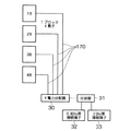
上記4素子1ブロックの無指向アレーアンテナを縦方向に複数段配列すれば、さらに素子アンテナ数の多い大型の無指向アレーアンテナを構成することができる。すなわち、例えば、図14に示すように、上記4素子1ブロックの無指向アレーアンテナを4ブロック(1B〜4B)多段接続すれば、16素子の無指向アレーアンテナを構成することができる。
【0040】
この場合、個々のブロック1B〜4Bの無指向アレーアンテナに接続された各給電ケーブル170は、4電力分配器30、分波器31を介して0.8GHz帯接続端子32および2GHz帯接続端子33に接続される。もちろん、これらの給電ケーブル170は、図1に示すグランドパターン230と導体板180との間に収納されるので、これらの給電ケーブル170およびその接続コネクタが指向性等に悪影響を与える虞はない。この4本の給電ケーブル180やそれを接続するためのコネクタを無造作に配置した場合、指向特性等の劣化を招くことになる。
なお、上記4本の給電ケーブル170の途中に移相器を挿入して、個々の素子アンテナにおけるビームのチルト角を変化させることも可能である。
【0041】
ところで、図2および図11に示したダイポールアンテナパターン13,13は、その給電点13a,13bがそれぞれ給電ラインパターン15a,15bを介して対応するダイポールアンテナパターン12,12の給電点12a,12bに接続されているが、図15に示すように、ダイポールアンテナパターン13,13を対応するダイポールアンテナパターン12,12から切離して形成することも可能である。
この場合、ダイポールアンテナパターン13,13は、図3および図12に示したプリント化給電回路20および200から切離されるが、共振によって適用周波数帯のダイポールアンテナとして作動することになる。
【0042】
また、図2および図11に示したダイポールアンテナパターン13,13は、それぞれ対応するダイポールアンテナパターン12,12の外側近傍に形成されているが、図16に示すように、ダイポールアンテナパターン12,12に相対向する一対の略U字状の切欠き部12cを設けることによって、このポールアンテナパターン12,12の内部にポールアンテナパターン13,13を形成することも可能である。
【0043】
以上においては、2周波に共用する無指向アンテナについて説明したが、3周波以上の波に共用する無指向アンテナも構成することができる。すなわち、例えば、3周波に共用する無指向アンテナを構成する場合には、図2に示したダイポールアンテナパターン13,13の側近に該ダイポールアンテナパターン13,13およびダイポールアンテナパターン12,12とは長さの異なる別のダイポールアンテナパターンをそれぞれ形成すれば良い。
また、図16の例では、ダイポールアンテナパターン13,13に上記した略U字状の切欠き部12cと同様の切欠き部を設けて、このポールアンテナパターン13,13内に別のダイポールアンテナパターンを形成すれば良い。
【0044】
【発明の効果】
本発明によれば、小型かつコンパクトな無指向アンテナおよびアレー構成の無指向アンテナを構成することができる。
また、複数の周波に共用することができる無指向アンテナおよびアレー構成の無指向アンテナを容易、かつ、コンパクト性を損なうことなく構成することができる。
そして、アレー構成の無指向アンテナにおいては、プリント化給電回路のグランドパターンとこれに対向するカバープレートとの間に給電ケーブルを配設することにより、この給電ケーブルによる影響を抑制して、より良好な指向特性を得ることができる。
【図面の簡単な説明】
【図1】本発明に係る無指向アンテナの実施の形態を示す断面図である。
【図2】プリント化ダイポールアンテナの一構成例を示す平面図である。
【図3】プリント化給電回路の一構成例を示す平面図である。
【図4】本発明に係る無指向アンテナのV.S.W.R特性を例示したグラフである。
【図5】本発明に係る無指向アンテナの周波数810.0MHzについての水平面内指向特性を例示したグラフである。
【図6】本発明に係る無指向アンテナの周波数885.0MHzについての水平面内指向特性を例示したグラフである。
【図7】本発明に係る無指向アンテナの周波数960.0MHzについての水平面内指向特性を例示したグラフである。
【図8】本発明に係る無指向アンテナの周波数1.92GHzについての水平面内指向特性を例示したグラフである。
【図9】本発明に係る無指向アンテナの周波数2.045GHzについての水平面内指向特性を例示したグラフである。
【図10】本発明に係る無指向アンテナの周波数2.17GHzについての水平面内指向特性を例示したグラフである。
【図11】プリント化ダイポールアレーアンテナの一構成例を示す平面図である。
【図12】プリント化ダイポールアレーアンテナ用プリント化給電回路の一構成例を示す平面図である。
【図13】本発明に係る無指向アレーアンテナのV.S.W.R特性を例示したグラフである。
【図14】本発明に係る16素子無指向アレーアンテナの電気接続形態の一例を示すブロック図。
【図15】ダイポールアンテナパターンの他の構成例を示した平面図である。
【図16】ダイポールアンテナパターンの更に別の構成例を示した平面図である。
【符号の説明】
10,100 プリント化ダイポールアンテナ
11,110,21,210 誘電体基板
12,13 ダイポールアンテナパターン
12a,12b,13a,13b 給電点
12c 切欠き部
15a,15b 給電ラインパターン
23,230 グランドパターン
170 給電ケーブル
180 導体板[0001]
TECHNICAL FIELD OF THE INVENTION
The present invention relates to a printed omnidirectional antenna.
[0002]
[Prior art]
In a simple base station for a mobile phone or the like, an omnidirectional antenna combined with a vertical dipole antenna or the like is used.
[0003]
[Problems to be solved by the invention]
The conventional omnidirectional antenna has a complicated structure, so that it is difficult to make it compact and compact. In particular, in the case of an array configuration, the structure is further complicated, and the arrangement of the power supply line requires time and effort.
The present invention has been made in view of such a situation, and an object of the present invention is to provide an omnidirectional antenna that can be configured to be small and compact.
[0004]
[Means for Solving the Problems]
The present invention relates to first and second printed dipole antennas in which a pair of parallel dipole antenna patterns are formed on a rectangular dielectric substrate, and dipole antenna patterns of the first and second printed dipole antennas. And a printed feed circuit in which a parallel feed circuit pattern formed on the dielectric substrate is connected to each of the first and second printed dipole antennas. along the longitudinal axis of the substrate, and is formed so as to be located symmetrically about the said axis, the first, the dielectric substrate of the second print of dipole antennas, each being formed on their with the dipole antenna pattern mutually parallel arranged to face the first One side and the other side of the dielectric substrate of the printed power supply circuit so that the dielectric substrate of the second printed dipole antenna and the dielectric substrate of the printed power supply circuit form an H-shaped cross section. The opposed first and second printed dipole antennas are located on the longitudinal axis of the dielectric substrate .
[0005]
According to the present invention, the substrate of the first printed dipole antenna, the substrate of the second printed dipole antenna, and the substrate of the printed power supply circuit are arranged so as to form an H-shaped cross section, so that they are small and compact. A compact omnidirectional antenna is configured.
[0006]
Dipole antenna patterns shorter in length than these dipole antenna patterns are formed in parallel and adjacent to the sides of each dipole antenna pattern in the first and second printed dipole antennas, respectively. Each short dipole antenna pattern can be configured to be connected to the power supply circuit pattern. According to this configuration, it is possible to share a plurality of frequencies.
[0007]
Dipole antenna patterns shorter in length than these dipole antenna patterns are formed in parallel and adjacent to the sides of each dipole antenna pattern in the first and second printed dipole antennas, respectively. Each short dipole antenna pattern may be configured to be separated from the power supply circuit pattern. According to this configuration, each of the short dipole antenna patterns performs a resonance operation, so that it is possible to share the dipole antenna patterns for a plurality of frequencies.
[0008]
A part of each dipole antenna pattern in the first and second printed dipole antennas is cut out, and a dipole antenna pattern shorter in length than these dipole antenna patterns is formed in each of these dipole antenna patterns. Each of the short dipole antenna patterns may be connected to the power supply circuit pattern. According to this configuration, a function shared by a plurality of frequencies can be realized with a more compact configuration.
[0009]
The present invention provides a first and a second printed dipole array antenna formed by cascading a plurality of pairs of parallel dipole antenna patterns in a longitudinal direction of a rectangular dielectric substrate, and the first and second printed dipole array antennas. A printed feed circuit formed on a dielectric substrate with a parallel feed circuit pattern connected to each dipole antenna pattern of the printed dipole array antenna, and a pair of dipoles in the first and second printed dipole antennas. antenna pattern, along the longitudinal axis of the dielectric substrate of those antennas, and is formed so as to be located symmetrically about the axial line, the dielectric of the first, second printing of dipole array antenna the body substrate, wherein each dipole antenna pattern mutually formed thereof With parallel arranged to counter, the first, as a dielectric substrate of a dielectric substrate and the printed of the feed circuit of the second print of dipole array antenna to form a H-shaped cross section, said print of One side and the other side of the dielectric substrate of the feeding circuit are respectively located on the longitudinal axis of the dielectric substrate of the first and second printed dipole array antennas facing each other.
[0010]
According to the present invention, the substrate of the first printed dipole array antenna, the substrate of the second printed dipole array antenna, and the substrate of the printed power supply circuit are arranged so as to form an H-shaped cross section. An omnidirectional antenna having a small and compact array configuration is configured.
[0011]
Dipole antenna patterns shorter in length than these dipole antenna patterns are formed in parallel and adjacent to the sides of each dipole antenna pattern in the first and second printed dipole array antennas, respectively. The short dipole antenna patterns can be connected to the power supply circuit pattern. According to this configuration, it is possible to share a plurality of frequencies.
[0012]
Dipole antenna patterns shorter in length than these dipole antenna patterns are formed in parallel and adjacent to the sides of each dipole antenna pattern in the first and second printed dipole array antennas, respectively. The short dipole antenna patterns can be separated from the power supply circuit pattern. According to this configuration, each of the short dipole antenna patterns performs a resonance operation, so that it is possible to share the dipole antenna patterns for a plurality of frequencies.
[0013]
A part of each dipole antenna pattern in the first and second printed dipole array antennas is cut out, and a dipole antenna pattern having a shorter length than these dipole antenna patterns is formed in each dipole antenna pattern. Each of the short dipole antenna patterns may be connected to the power supply circuit pattern. According to this configuration, a function shared by a plurality of frequencies can be realized more compactly.
[0014]
A shield post pattern can be formed between each pair of dipole antenna patterns in the first and second printed dipole array antennas. According to this configuration, interference between pairs of adjacent dipole antenna patterns is suppressed, and S. W. The R characteristic can be further improved.
[0015]
The power supply circuit pattern of the printed power supply circuit includes a ground pattern along a longitudinal direction of a substrate of the power supply circuit, and a cover plate made of a conductive material is disposed to face the ground pattern. The power supply cable can be arranged in a space formed between the ground patterns. According to this configuration, the influence of the power supply cable can be reduced.
[0016]
BEST MODE FOR CARRYING OUT THE INVENTION
FIG. 1 is a sectional view showing an embodiment of the omnidirectional antenna according to the present invention. This antenna is used, for example, in a simple base station for mobile phones.
This omnidirectional antenna has a configuration in which a pair of printed
[0017]
As shown in FIG. 2, the printed
[0018]
In this embodiment, the
[0019]
The
The
[0020]
One of the
[0021]
On the other hand, as shown in FIG. 3, the printed
[0022]
The
The
[0023]
As shown in FIG. 1, the
[0024]
Each of the
[0025]
The omnidirectional antenna according to this embodiment having such a configuration is installed such that the
[0026]
As shown in FIG. 1, in this omnidirectional antenna, four
Since the directivity in the horizontal plane of each of the four vertically oriented
[0027]
Similarly, the directivity in the horizontal plane of each of the four vertically oriented
That is, the antenna structure including the four
[0028]
FIG. 4 is a block diagram of the omnidirectional antenna according to this embodiment. S. W. It shows an R (voltage standing wave ratio) characteristic. In FIG. 4, the scale on the horizontal axis is given in 200 MHz steps, and the scale on the vertical axis is given in 5 dB steps.
As is apparent from FIG. 4, the omnidirectional antenna according to this embodiment has a good V.I.D. in the used frequency band of 810 to 960 MHz due to the operation of the antenna structure composed of four
[0029]
On the other hand, FIG. 5, FIG. 6 and FIG. 7 show the directional characteristics in the horizontal plane of the omnidirectional antenna according to this embodiment at frequencies of 810.0 MHz, 885.0 MHz and 960.0 MHz, and FIG. FIG. 10 shows the directional characteristics in the horizontal plane for the frequencies 1.92 GHz, 2.04 GHz, and 2.17 GHz of the antenna, respectively.
As is apparent from these figures, the omnidirectional antenna according to this embodiment has a good circular in-plane directional characteristic in a used frequency band.
In short, the antenna according to this embodiment has a good V.I. S, W. It acts as a dual frequency omnidirectional antenna having an R characteristic and a directional characteristic in a horizontal plane.
[0030]
Based on the configuration of the omnidirectional antenna, it is also possible to configure a dual-frequency omnidirectional array antenna. In this case, a pair of a printed
[0031]
The printed
In addition, between each pair of patterns, the shield post pattern 16 is formed by a thin film conductor. The arrangement interval L7 of each pattern set is set to about 0.44λ (885 MHz) and 1.00λ (2.045 GHz).
[0032]
On the other hand, the printed
[0033]
The
[0034]
As shown in FIG. 1, the
Further, the
[0035]
In the omni-directional array antenna according to this embodiment having such a configuration, the branch end of each
[0036]
As shown in FIG. 1, a
A
[0037]
This omnidirectional array antenna has a configuration in which the omnidirectional antenna described above is used as an element antenna, and four such element antennas are linearly arranged. That is, the array antenna has a four-element one-block configuration. V. of individual element antennas S, W. The R characteristic is as shown in FIG. Therefore, as shown in FIG. 13, this omnidirectional array antenna also has a good V.V. frequency band in the used frequency band of 810 to 960 MHz and 1.92 to 2.17 GHz. S, W. The R characteristic is shown.
[0038]
This omnidirectional array antenna can be configured very easily only by combining each of the printed
The shield post pattern 16 shields the adjacent
[0039]
By arranging the four-element one-block omnidirectional array antenna in a plurality of stages in the vertical direction, a large omnidirectional array antenna having a larger number of element antennas can be configured. That is, for example, as shown in FIG. 14, if the four-element one-block omnidirectional array antenna is connected in multiple stages of four blocks (1B to 4B), a sixteen-element omnidirectional array antenna can be configured.
[0040]
In this case, the
In addition, it is also possible to insert a phase shifter in the middle of the four
[0041]
By the way, the
In this case, the
[0042]
The
[0043]
In the above, the omnidirectional antenna shared by two frequencies has been described, but an omnidirectional antenna shared by three or more frequencies can also be configured. That is, for example, when an omnidirectional antenna shared by three frequencies is configured, the
In the example of FIG. 16, a notch similar to the above-described substantially
[0044]
【The invention's effect】
According to the present invention, a small and compact omnidirectional antenna and an omnidirectional antenna having an array configuration can be configured.
In addition, the omnidirectional antenna and the omnidirectional antenna having an array configuration that can be shared by a plurality of frequencies can be easily configured without impairing compactness.
In an omnidirectional antenna having an array configuration, a power supply cable is provided between a ground pattern of a printed power supply circuit and a cover plate facing the power supply circuit, so that the influence of the power supply cable is suppressed, and the antenna is further improved. Directional characteristics can be obtained.
[Brief description of the drawings]
FIG. 1 is a sectional view showing an embodiment of an omnidirectional antenna according to the present invention.
FIG. 2 is a plan view illustrating a configuration example of a printed dipole antenna.
FIG. 3 is a plan view illustrating a configuration example of a printed power supply circuit.
FIG. 4 shows the V.I. of the omnidirectional antenna according to the present invention. S. W. It is a graph which illustrated R characteristic.
FIG. 5 is a graph illustrating a directional characteristic in a horizontal plane for a frequency of 810.0 MHz of the omnidirectional antenna according to the present invention.
FIG. 6 is a graph illustrating the directional characteristics in the horizontal plane of the omnidirectional antenna according to the present invention at a frequency of 885.0 MHz.
FIG. 7 is a graph illustrating directional characteristics in a horizontal plane of the omnidirectional antenna according to the present invention at a frequency of 960.0 MHz.
FIG. 8 is a graph illustrating a directional characteristic in a horizontal plane at a frequency of 1.92 GHz of the omnidirectional antenna according to the present invention.
FIG. 9 is a graph illustrating the directional characteristics in a horizontal plane of the omnidirectional antenna according to the present invention at a frequency of 2.045 GHz.
FIG. 10 is a graph illustrating a directional characteristic in a horizontal plane at a frequency of 2.17 GHz of the omnidirectional antenna according to the present invention.
FIG. 11 is a plan view showing a configuration example of a printed dipole array antenna.
FIG. 12 is a plan view showing a configuration example of a printed power supply circuit for a printed dipole array antenna.
FIG. 13 shows the V.I. S. W. It is a graph which illustrated R characteristic.
FIG. 14 is a block diagram showing an example of an electrical connection configuration of a 16-element omnidirectional array antenna according to the present invention.
FIG. 15 is a plan view showing another configuration example of the dipole antenna pattern.
FIG. 16 is a plan view showing still another configuration example of the dipole antenna pattern.
[Explanation of symbols]
10, 100 Printed
Claims (10)
前記第1および第2のプリント化ダイポールアンテナの各ダイポールアンテナパターンにそれぞれ接続される並列給電回路パターンを誘電体基板に形成したプリント化給電回路と、を備え、
前記第1および第2のプリント化ダイポールアンテナにおける一対のダイポールアンテナパターンは、それらのアンテナの誘電体基板の長手方向軸線に沿うように、かつ、該軸線を中心として対称に位置するように形成され、
前記第1、第2のプリント化ダイポールアンテナの誘電体基板を、それらに形成された前記各ダイポールアンテナパターン相互が対向するように平行配置するとともに、前記第1、第2のプリント化ダイポールアンテナの誘電体基板と前記プリント化給電回路の誘電体基板とがH状の断面を形成するように、前記プリント化給電回路の誘電体基板の一側および他側を前記対向する第1、第2のプリント化ダイポールアンテナの誘電体基板の長手方向軸線上にそれぞれ位置させたことを特徴とする無指向アンテナ。A first and a second printed dipole antenna in which a pair of parallel dipole antenna patterns are formed on a rectangular dielectric substrate;
A printed power supply circuit in which a parallel power supply circuit pattern connected to each of the dipole antenna patterns of the first and second printed dipole antennas is formed on a dielectric substrate,
The pair of dipole antenna patterns in the first and second printed dipole antennas are formed so as to be along the longitudinal axis of the dielectric substrate of those antennas and to be symmetrical about the axis. ,
The dielectric substrates of the first and second printed dipole antennas are arranged in parallel so that the respective dipole antenna patterns formed thereon face each other , and the dielectric substrates of the first and second printed dipole antennas are arranged . First and second facing sides of one side and the other side of the dielectric substrate of the printed power supply circuit so that the dielectric substrate and the dielectric substrate of the printed power supply circuit form an H-shaped cross section. An omnidirectional antenna, wherein the antenna is located on a longitudinal axis of a dielectric substrate of the printed dipole antenna.
前記長さの短かい各ダイポールアンテナパターンを前記給電回路パターンに接続したことを特徴とする請求項1に記載の無指向アンテナ。Forming a dipole antenna pattern shorter in length than these dipole antenna patterns in parallel and adjacent to each of the dipole antenna patterns in the first and second printed dipole antennas,
The omnidirectional antenna according to claim 1, wherein each of the short dipole antenna patterns is connected to the power supply circuit pattern.
前記長さの短かい各ダイポールアンテナパターンを前記給電回路パターンから切離したことを特徴とする請求項1に記載の無指向アンテナ。Forming a dipole antenna pattern shorter in length than these dipole antenna patterns in parallel and adjacent to each of the dipole antenna patterns in the first and second printed dipole antennas,
The omnidirectional antenna according to claim 1, wherein each of the short dipole antenna patterns is separated from the power supply circuit pattern.
前記長さの短かい各ダイポールアンテナパターンを前記給電回路パターンに接続したことを特徴とする請求項1に記載の無指向アンテナ。A part of each dipole antenna pattern in the first and second printed dipole antennas is cut out, and a dipole antenna pattern having a shorter length than these dipole antenna patterns is formed in each of these dipole antenna patterns;
The omnidirectional antenna according to claim 1, wherein each of the short dipole antenna patterns is connected to the power supply circuit pattern.
前記第1および第2のプリント化ダイポールアレーアンテナの各ダイポールアンテナパターンにそれぞれ接続される並列給電回路パターンを誘電体基板に形成したプリント化給電回路と、を備え、
前記第1および第2のプリント化ダイポールアンテナにおける一対のダイポールアンテナパターンは、それらのアンテナの誘電体基板の長手方向軸線に沿うように、かつ、該軸線を中心として対称に位置するように形成され、
前記第1、第2のプリント化ダイポールアレーアンテナの誘電体基板を、それらに形成された前記各ダイポールアンテナパターン相互が対向するように平行配置するとともに、前記第1、第2のプリント化ダイポールアレーアンテナの誘電体基板と前記プリント化給電回路の誘電体基板とがH状の断面を形成するように、前記プリント化給電回路の誘電体基板の一側および他側を前記対向する第1、第2のプリント化ダイポールアレーアンテナの誘電体基板の長手方向軸線上にそれぞれ位置させたことを特徴とする無指向アンテナ。First and second printed dipole array antennas formed by cascading a plurality of pairs of parallel dipole antenna patterns in a longitudinal direction of a rectangular dielectric substrate;
A printed power supply circuit formed on a dielectric substrate with a parallel power supply circuit pattern connected to each of the dipole antenna patterns of the first and second printed dipole array antennas,
The pair of dipole antenna patterns in the first and second printed dipole antennas are formed so as to be along the longitudinal axis of the dielectric substrate of those antennas and to be symmetrical about the axis. ,
Dielectric substrates of the first and second printed dipole array antennas are arranged in parallel so that the respective dipole antenna patterns formed thereon face each other, and the first and second printed dipole arrays are arranged. The first and second sides of one side and the other side of the dielectric substrate of the printed power supply circuit are opposed so that the dielectric substrate of the antenna and the dielectric substrate of the printed power supply circuit form an H-shaped cross section. 2. The omnidirectional antenna according to claim 2, wherein the printed dipole array antenna is positioned on the longitudinal axis of the dielectric substrate .
前記長さの短かい各ダイポールアンテナパターンを前記給電回路パターンに接続したことを特徴とする請求項5に記載の無指向アンテナ。Forming dipole antenna patterns shorter in length than these dipole antenna patterns in parallel and adjacent to the side of each dipole antenna pattern in the first and second printed dipole array antennas, respectively;
The omnidirectional antenna according to claim 5, wherein each of the short dipole antenna patterns is connected to the power supply circuit pattern.
前記長さの短かい各ダイポールアンテナパターンを前記給電回路パターンから切離したことを特徴とする請求項5に記載の無指向アンテナ。Forming dipole antenna patterns shorter in length than these dipole antenna patterns in parallel and adjacent to the side of each dipole antenna pattern in the first and second printed dipole array antennas, respectively;
The omnidirectional antenna according to claim 5, wherein each of the short dipole antenna patterns is separated from the power supply circuit pattern.
前記長さの短かい各ダイポールアンテナパターンを前記給電回路パターンに接続したことを特徴とする請求項5に記載の無指向アンテナ。A part of each dipole antenna pattern in the first and second printed dipole array antennas is cut out, and a dipole antenna pattern having a shorter length than these dipole antenna patterns is formed in each of the dipole antenna patterns. ,
The omnidirectional antenna according to claim 5, wherein each of the short dipole antenna patterns is connected to the power supply circuit pattern.
Priority Applications (1)
| Application Number | Priority Date | Filing Date | Title |
|---|---|---|---|
| JP2001215271A JP3553032B2 (en) | 2001-07-16 | 2001-07-16 | Omnidirectional antenna |
Applications Claiming Priority (1)
| Application Number | Priority Date | Filing Date | Title |
|---|---|---|---|
| JP2001215271A JP3553032B2 (en) | 2001-07-16 | 2001-07-16 | Omnidirectional antenna |
Publications (2)
| Publication Number | Publication Date |
|---|---|
| JP2003032034A JP2003032034A (en) | 2003-01-31 |
| JP3553032B2 true JP3553032B2 (en) | 2004-08-11 |
Family
ID=19049947
Family Applications (1)
| Application Number | Title | Priority Date | Filing Date |
|---|---|---|---|
| JP2001215271A Expired - Lifetime JP3553032B2 (en) | 2001-07-16 | 2001-07-16 | Omnidirectional antenna |
Country Status (1)
| Country | Link |
|---|---|
| JP (1) | JP3553032B2 (en) |
Families Citing this family (8)
| Publication number | Priority date | Publication date | Assignee | Title |
|---|---|---|---|---|
| US7190319B2 (en) * | 2001-10-29 | 2007-03-13 | Forster Ian J | Wave antenna wireless communication device and method |
| JP3900100B2 (en) * | 2003-03-20 | 2007-04-04 | 日立電線株式会社 | Substrate antenna |
| JP4170823B2 (en) * | 2003-06-02 | 2008-10-22 | 電気興業株式会社 | Multi-frequency dipole antenna |
| JP2005033517A (en) * | 2003-07-14 | 2005-02-03 | Denki Kogyo Co Ltd | Antenna device |
| JP4452081B2 (en) * | 2004-01-09 | 2010-04-21 | 八木アンテナ株式会社 | Parallel feeding collinear antenna |
| JP3983237B2 (en) * | 2004-09-03 | 2007-09-26 | 電気興業株式会社 | Antenna device |
| JP4027950B2 (en) * | 2005-06-23 | 2007-12-26 | 電気興業株式会社 | Omnidirectional antenna |
| CN115528419B (en) * | 2022-01-07 | 2024-03-26 | 荣耀终端有限公司 | Terminal antenna |
-
2001
- 2001-07-16 JP JP2001215271A patent/JP3553032B2/en not_active Expired - Lifetime
Also Published As
| Publication number | Publication date |
|---|---|
| JP2003032034A (en) | 2003-01-31 |
Similar Documents
| Publication | Publication Date | Title |
|---|---|---|
| US6762729B2 (en) | Slotted bow tie antenna with parasitic element, and slotted bow tie array antenna with parasitic element | |
| US6593891B2 (en) | Antenna apparatus having cross-shaped slot | |
| US6933905B2 (en) | RF card with conductive strip | |
| US6549169B1 (en) | Antenna for mobile wireless communications and portable-type wireless apparatus using the same | |
| CN112088465B (en) | Antenna | |
| JP2004328717A (en) | Diversity antenna device | |
| EP0818846A2 (en) | Planar antenna | |
| US20050237244A1 (en) | Compact RF antenna | |
| US20030112200A1 (en) | Horizontally polarized printed circuit antenna array | |
| KR100449396B1 (en) | Patch antenna and electronic equipment using the same | |
| KR20020011141A (en) | Integrable dual-band antenna | |
| KR20200011500A (en) | Tripolar Current Loop Radiating Element with Integrated Circular Polarization Feed | |
| US6650299B2 (en) | Antenna apparatus | |
| US20230011271A1 (en) | Antenna module and electronic device | |
| JP3553032B2 (en) | Omnidirectional antenna | |
| KR102064175B1 (en) | Double Circularly Polarized Antenna | |
| WO2002023669A1 (en) | A dual polarised antenna | |
| JP2002319809A (en) | Antenna system | |
| JP2007124346A (en) | Antenna element and array type antenna | |
| US11563271B2 (en) | Antenna array with ABFN circuitry | |
| JP4452081B2 (en) | Parallel feeding collinear antenna | |
| US20230008852A1 (en) | Transmission line | |
| JP2709383B2 (en) | Circularly polarized microstrip antenna device | |
| CN215418583U (en) | Microstrip antenna | |
| JPH05206729A (en) | Array antenna system |
Legal Events
| Date | Code | Title | Description |
|---|---|---|---|
| A521 | Written amendment |
Free format text: JAPANESE INTERMEDIATE CODE: A523 Effective date: 20040216 |
|
| TRDD | Decision of grant or rejection written | ||
| A01 | Written decision to grant a patent or to grant a registration (utility model) |
Free format text: JAPANESE INTERMEDIATE CODE: A01 Effective date: 20040406 |
|
| A61 | First payment of annual fees (during grant procedure) |
Free format text: JAPANESE INTERMEDIATE CODE: A61 Effective date: 20040427 |
|
| R150 | Certificate of patent or registration of utility model |
Free format text: JAPANESE INTERMEDIATE CODE: R150 Ref document number: 3553032 Country of ref document: JP Free format text: JAPANESE INTERMEDIATE CODE: R150 |
|
| R250 | Receipt of annual fees |
Free format text: JAPANESE INTERMEDIATE CODE: R250 |
|
| FPAY | Renewal fee payment (event date is renewal date of database) |
Free format text: PAYMENT UNTIL: 20090514 Year of fee payment: 5 |
|
| R250 | Receipt of annual fees |
Free format text: JAPANESE INTERMEDIATE CODE: R250 |
|
| FPAY | Renewal fee payment (event date is renewal date of database) |
Free format text: PAYMENT UNTIL: 20100514 Year of fee payment: 6 |
|
| R250 | Receipt of annual fees |
Free format text: JAPANESE INTERMEDIATE CODE: R250 |
|
| FPAY | Renewal fee payment (event date is renewal date of database) |
Free format text: PAYMENT UNTIL: 20100514 Year of fee payment: 6 |
|
| FPAY | Renewal fee payment (event date is renewal date of database) |
Free format text: PAYMENT UNTIL: 20110514 Year of fee payment: 7 |
|
| R250 | Receipt of annual fees |
Free format text: JAPANESE INTERMEDIATE CODE: R250 |
|
| FPAY | Renewal fee payment (event date is renewal date of database) |
Free format text: PAYMENT UNTIL: 20120514 Year of fee payment: 8 |
|
| R250 | Receipt of annual fees |
Free format text: JAPANESE INTERMEDIATE CODE: R250 |
|
| FPAY | Renewal fee payment (event date is renewal date of database) |
Free format text: PAYMENT UNTIL: 20130514 Year of fee payment: 9 |
|
| R250 | Receipt of annual fees |
Free format text: JAPANESE INTERMEDIATE CODE: R250 |
|
| FPAY | Renewal fee payment (event date is renewal date of database) |
Free format text: PAYMENT UNTIL: 20130514 Year of fee payment: 9 |
|
| R250 | Receipt of annual fees |
Free format text: JAPANESE INTERMEDIATE CODE: R250 |
|
| R250 | Receipt of annual fees |
Free format text: JAPANESE INTERMEDIATE CODE: R250 |
|
| R250 | Receipt of annual fees |
Free format text: JAPANESE INTERMEDIATE CODE: R250 |
|
| R250 | Receipt of annual fees |
Free format text: JAPANESE INTERMEDIATE CODE: R250 |
|
| R250 | Receipt of annual fees |
Free format text: JAPANESE INTERMEDIATE CODE: R250 |
|
| R250 | Receipt of annual fees |
Free format text: JAPANESE INTERMEDIATE CODE: R250 |
|
| EXPY | Cancellation because of completion of term |