JP3550573B2 - Power converter - Google Patents
Power converter Download PDFInfo
- Publication number
- JP3550573B2 JP3550573B2 JP17616998A JP17616998A JP3550573B2 JP 3550573 B2 JP3550573 B2 JP 3550573B2 JP 17616998 A JP17616998 A JP 17616998A JP 17616998 A JP17616998 A JP 17616998A JP 3550573 B2 JP3550573 B2 JP 3550573B2
- Authority
- JP
- Japan
- Prior art keywords
- voltage
- switching
- power supply
- voltage source
- bypass
- Prior art date
- Legal status (The legal status is an assumption and is not a legal conclusion. Google has not performed a legal analysis and makes no representation as to the accuracy of the status listed.)
- Expired - Fee Related
Links
Images


Landscapes
- Stand-By Power Supply Arrangements (AREA)
Description
【0001】
【発明の属する技術分野】
この発明はUPS(無停電電源装置)などのように、直流を交流に変換する直流/交流電力変換器と、バイパス電源とを切り換えて負荷に電力を供給する電力変換装置に関するものである。
【0002】
【従来の技術】
図22は従来の電力変換装置を示すもので、例えば、電気書院発行「無停電電源装置(UPS)導入実践ガイド」(1989年2月25日第1版第1刷発行)のP56〜61に記載の無瞬断バイパス切換方式を説明するものである。図において、1は直流電力を供給する直流電圧源、2は直流を交流に変換するインバータ、3はインバータ2の出力電圧にフィルタをかけ不必要な周波数成分を減衰させるフィルタ回路、4はフィルタ回路3の出力につながったスイッチ、6は商用電源であるバイパス電源、5はバイパス電源6の出力につながったスイッチ、7はスイッチ4およびスイッチ5を介してそれぞれインバータ2およびバイパス電源6に接続された負荷である。特に、前記スイッチ5はサイリスタ等の半導体で構成され高速動作ができるスイッチである。
【0003】
また、20はフィルタ回路3の出力電圧を検出する電圧センサ、21はバイパス電源6の電圧を検出する電圧センサ、22はスイッチ4、5の動作指令を発生する切換指令発生回路で、その出力信号である切換指令は切換が完了するまで出力し続けるよう動作する。また、24は発振器、25は電圧センサ20、21の出力であるインバータ電圧とバイパス電圧とを同期させるための位相情報と同期状態信号を出力する同期制御回路で、バイパス電源6の周波数が異常な場合は発振器24の出力を位相情報として出力する。23は切換指令発生回路22と同期制御回路25の出力を受けてスイッチ4、5のオン・オフ信号を出力する切換制御回路、26は電圧振幅指令を発生する回路、27は電圧振幅指令と位相情報とからインバータ2の電圧指令を生成する電圧指令発生回路、28は電圧指令とインバータ電圧を入力しインバータ電圧を指令通りとなるよう制御する電圧制御回路、29は電圧制御回路28の出力を受けてインバータの駆動指令を出力する駆動回路である。
【0004】
図23は、負荷7に供給する電源をインバータ2からバイパス電源6に切り換えるときのスイッチ4および5の動作指令のタイミングチャートを示したものである。
【0005】
次に動作について説明する。負荷7への電源をインバータ2からバイパス電源6に切り換える場合、切換の前後で負荷に電圧の急変を起こさないようにするため、同期制御回路25によりインバータ2はバイパス電源6と同期(同一周波数・同一位相)運転を行う。切換指令発生回路22から、負荷7への電源を、インバータ2からバイパス電源6に切り換える指令が出力されたとき、インバータ2の出力がバイパス電源6の電圧に同期していると、図23に示すタイミングチャートのようにバイパス電源6のスイッチ5をオンし、スイッチ4と5を共にオンした状態(ラップ状態)を作りながらインバータ2のスイッチ4をオフさせることで負荷に電圧変動を起こすことなく電源を切り換える。
【0006】
【発明が解決しようとする課題】
従来の電力変換装置は以上のように構成されているので、バイパス電源6の電圧および周波数が所定の範囲(例えば、電圧は基準値±10%以内、周波数は基準値±1%以内)にあって、同期制御回路25によりバイパス電源6に同期する電圧をインバータ2が出力している場合は問題ないが、バイパス電源6の電圧または周波数が上記所定の範囲を越えて同期制御が実施されていない非同期の場合には、スイッチ4と5をラップさせながら切り換えたりインバータ2を停止した瞬間にバイパス電源6の高速スイッチ5をオンさせたりすると、2つの電源の電圧差により負荷機器内の変圧器やコンデンサに過大な電流が流れたり電圧が低下したりなどして負荷システムの停止を招く恐れがある。従って、非同期のときはインバータ2とバイパス電源6との間の切換ができないので、メンテナンス時等に保守電源に電圧を瞬断することなく切り換えたり、バイパス給電からインバータ給電に切り換えること等ができないという問題点があった。
【0007】
この発明は上記のような課題を解決するためになされたもので、バイパス電源とインバータ電源とが正常な同期がとれていない非同期の状態でも負荷電圧に変動を与えることなく両電源間の切り換えを可能とする電力変換装置を得ることを目的とする。
【0008】
【課題を解決するための手段】
この発明の電力変換装置は、電圧指令に応じて交流電圧を出力可能な交流電圧源、この交流電圧源と負荷との接離を行う第1の開閉手段、バイパス電源、およびこのバイパス電源と上記負荷との接離を行う第2の開閉手段を備え、上記第1および第2の開閉手段を操作することにより、上記負荷に接続する電源を、上記交流電圧源と上記バイパス電源とのいずれかに切り換えて上記負荷へ電力を供給する電力変換装置において、
上記交流電圧源および上記バイパス電源が三相電源であり、上記電源の切換指令を発生する切換指令発生回路、上記交流電圧源とバイパス電源との電圧差が所定の範囲内になったとき切換許可信号を出力する切換判定回路、および上記切換指令と上記切換許可信号とを入力して上記第1および第2の開閉手段を開閉操作する切換制御回路を備え、上記切換 判定回路は、三相各相毎に上記交流電圧源とバイパス電源との瞬時電圧差を演算する減算器、これら各減算器の出力の絶対値を加算する加算器、およびこの加算器の出力が所定の値内になったとき上記切換許可信号を出力する比較器を有するものである。
【0009】
また、この発明の電力変換装置は、電圧指令に応じて交流電圧を出力可能な交流電圧源、この交流電圧源と負荷との接離を行う第1の開閉手段、バイパス電源、およびこのバイパス電源と上記負荷との接離を行う第2の開閉手段を備え、上記第1および第2の開閉手段を操作することにより、上記負荷に接続する電源を、上記交流電圧源と上記バイパス電源とのいずれかに切り換えて上記負荷へ電力を供給する電力変換装置において、
上記交流電圧源および上記バイパス電源が三相電源であり、上記電源の切換指令を発生する切換指令発生回路、上記交流電圧源の電圧とバイパス電源の電圧との振幅差および位相差が所定の範囲内になったとき切換許可信号を出力する切換判定回路、および上記切換指令と上記切換許可信号とを入力して上記第1および第2の開閉手段を開閉操作する切換制御回路を備え、上記切換判定回路は、上記交流電圧源の三相電圧をd軸とq軸の二相に変換する第1の3/2変換回路、上記バイパス電源の三相電圧をd軸とq軸の二相に変換する第2の3/2変換回路、上記両3/2変換回路の出力のd軸成分同士の瞬時値差を演算する第1の減算器、上記両3/2変換回路の出力のq軸成分同士の瞬時値差を演算する第2の減算器、上記両減算器の出力の2乗和の平方根を演算する振幅検出回路、およびこの振幅検出回路の出力が所定の値内になったとき上記切換許可信号を出力する比較器を有するものである。
【0010】
また、この発明の電力変換装置は、負荷に接続する電源を、交流電圧源からバイパス電源に切り換える切換指令が出力された場合、上記交流電圧源の電圧とバイパス電源の電圧との振幅差となる上記第1の減算器の出力を、上記交流電圧源の電圧指令に加算する加算器を備えたものである。
【0011】
また、この発明の電力変換装置は、交流電圧源が故障でその出力が停止した場合、上記停止直前の電圧出力を記憶する記憶回路を備え、切換判定回路は、上記記憶回路に記憶された電圧とバイパス電源の電圧との振幅差および位相差が所定の範囲内になったとき切換許可信号を出力するようにしたものである。
【0012】
また、この発明の電力変換装置は、所定の電圧および周波数の範囲内で、交流電圧源の電圧指令をバイパス電源の電圧に一致させ上記両電源の電圧を同期させる同期制御回路を備え、負荷に接続する電源を、上記交流電圧源からバイパス電源に切り換える切換指令が出力された場合、上記同期が成立しているときは上記切換に係る第1および第2の開閉手段の開閉操作中上記交流電圧源の出力を維持し、上記同期が成立していない非同期時は上記切換に係る上記第2の開閉手段の閉動作と同時に上記交流電圧源の出力を停止するようにしたものである。
【0013】
また、この発明の電力変換装置は、電圧指令に応じて交流電圧を出力可能な交流電圧源、この交流電圧源と負荷との接離を行う第1の開閉手段、バイパス電源、およびこのバイパス電源と上記負荷との接離を行う第2の開閉手段を備え、上記第1および第2の開閉手段を操作することにより、上記負荷に接続する電源を、上記交流電圧源と上記バイパス電源とのいずれかに切り換えて上記負荷へ電力を供給する電力変換装置において、
上記電源の切換指令を発生する切換指令発生回路、上記交流電圧源とバイパス電源との電圧差を検出し、この電圧差が所定の範囲内になったとき切換許可信号を出力する切換判定回路、上記切換指令と上記切換許可信号とを入力して上記第1および第2の開閉手段を開閉操作する切換制御回路、および所定の電圧および周波数の範囲内で、上記交流電圧源の電圧指令を上記バイパス電源の電圧に一致させ上記両電源の電圧を同期させる同期制御回路を備え、負荷に接続する電源を、上記交流電圧源からバイパス電源に切り換える切換 指令が出力された場合、上記同期が成立しているときは上記切換に係る第1および第2の開閉手段の開閉操作中上記交流電圧源の出力を維持し、上記同期が成立していない非同期時は上記切換に係る上記第2の開閉手段の閉動作と同時に上記交流電圧源の出力を停止するようにしたものである。
【0014】
また、この発明の電力変換装置は、電圧指令に応じて交流電圧を出力可能な交流電圧源、この交流電圧源と負荷との接離を行う第1の開閉手段、バイパス電源、およびこのバイパス電源と上記負荷との接離を行う第2の開閉手段を備え、上記第1および第2の開閉手段を操作することにより、上記負荷に接続する電源を、上記交流電圧源と上記バイパス電源とのいずれかに切り換えて上記負荷へ電力を供給する電力変換装置において、
上記電源の切換指令を発生する切換指令発生回路、上記交流電圧源とバイパス電源との電圧差を検出し、この電圧差が所定の範囲内になったとき切換許可信号を出力する切換判定回路、上記切換指令と上記切換許可信号とを入力して上記第1および第2の開閉手段を開閉操作する切換制御回路、所定の電圧および周波数の範囲内で、上記交流電圧源の電圧指令を上記バイパス電源の電圧に一致させ上記両電源の電圧を同期させる同期制御回路、および負荷に接続する電源を、上記交流電圧源からバイパス電源に切り換えるときと上記バイパス電源から交流電圧源に切り換えるときとで上記所定の電圧および周波数の範囲の設定を切り換える範囲切換回路を備えたものである。
【0015】
また、この発明の電力変換装置は、所定の電圧および周波数の範囲内で、交流電圧源の電圧指令をバイパス電源の電圧に一致させ上記両電源の電圧を同期させる同期制御回路、および負荷に接続する電源を、上記交流電圧源からバイパス電源に切り換えるときと上記バイパス電源から交流電圧源に切り換えるときとで上記所定の電圧および周波数の範囲の設定を切り換える範囲切換回路を備えたものである。
【0016】
【発明の実施の形態】
実施の形態1.
図1はこの発明の実施の形態1における電力変換装置を示す構成図である。図において、1は直流電圧源、2は直流電圧源1の直流を交流に変換し電圧指令に応じて交流電圧を出力可能な交流電圧源としてのインバータ、3はフィルタ回路、4はインバータ2と負荷7との接離を行う第1の開閉手段としてのスイッチ、5は商用電源等のバイパス電源6と負荷7との接離を行う第2の開閉手段としてのスイッチである。
【0017】
20はフィルタ回路3の出力電圧を検出する電圧センサ、21はバイパス電源6の電圧を検出する電圧センサ、22は両電源2、6の切換指令を発生する切換指令発生回路、23は切換指令発生回路22からの切換指令と後述する切換判定回路30からの切換許可信号とを入力してスイッチ4,5にオン・オフ信号を出力する切換制御回路、25は両電圧センサ20,21からの信号を入力して動作する同期制御回路で、バイパス電源の電圧および周波数が所定の範囲(例えば、電圧は基準値±10%以内、周波数は基準値±1%以内)にあるときは、両入力電圧信号が同期するよう電圧指令発生回路27に信号を送出して同期制御がなされる。バイパス電源6の電圧または周波数が上記所定の範囲外の場合は、発振器24からの信号を入力して位相情報を電圧指令発生回路27に送出し、電圧指令発生回路27はこの位相情報と電圧振幅指令発生回路26の電圧振幅指令とに基づき電圧指令を出力する。この場合は、両電源2、6の電圧が同期しない非同期制御となる。
【0018】
28は電圧指令と電圧センサ20からの電圧信号とを入力し、インバータ2の出力電圧が指令通りとなるよう制御する電圧制御回路、29は電圧制御回路28の出力を受けてインバータ2のスイッチング素子に駆動指令を出力する駆動回路である。
30は電圧センサ20からの電圧信号(インバータ電圧)と電圧センサ21からの電圧信号(バイパス電圧)とを入力し切換許可信号を出力する切換判定回路である。
【0019】
図2は、電力変換装置が単相システムであるときの切換判定回路30aの内部回路構成を示したもので、100はインバータ電圧からバイパス電圧を減算する減算器、101は減算器100の出力であるバイパス電圧とインバータ電圧との電圧差と予め設定されたその許容値とを比較する比較器である。
【0020】
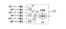
図3は電力変換装置が3相システムであるときの切換判定回路30bの内部回路構成を示したもので、102,103,104は各相毎にインバータ電圧からバイパス電圧を減算する減算器、105は減算器102,103,104の各出力の絶対値を加算する加算器、106は加算器105の出力であるバイパス電圧とインバータ電圧との電圧差と予め設定されたその許容値とを比較する比較器である。
【0021】
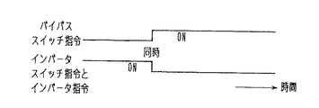
図4は切換制御回路30a、30bから出力されたスイッチ4、5の動作指令のタイミングチャートで、バイパススイッチ4のタイミングでインバータ2も瞬時に動作する。
【0022】
次に動作について説明する。図2(または図3)の切換判定回路30a(30b)で、インバータ電圧とバイパス電圧との偏差を検出し、その偏差が切換時に発生する電圧変化量として許容できる値かどうかを比較器101(106)で判断し、許容できれば切換許可信号を切換制御回路23に出力する。従って、インバータ電圧とバイパス電圧とに偏差がなければ切換許可信号は許可状態となり、切換制御回路23は切換指令が入力されていれば図4のタイミングチャートに示すようにインバータ2とインバータスイッチ4をオフすると同時にスイッチ5をオンさせる。インバータ2とスイッチ5とは高速に動作するので電圧差や瞬断を発生させることなく切り換えることができる。
上述した同期制御が実行されているときは、インバータ電圧とバイパス電圧とは一致しているので、切換判定回路30a(30b)は常時、切換許可信号を出力しており、切換指令が出力されると直ちに切換動作がなされるが、以上で説明したように、同期制御がなされていない非同期のときも一瞬の電圧の一致を検出し切り換えることができる。
【0023】
実施の形態2.
図5はこの発明の実施の形態2における電力変換装置の切換判定回路の内部回路構成を示す図である。なお、実施の形態1ではインバータ電圧とバイパス電圧とが一瞬でも一致したとき切換できるように構成したため、両電圧の位相が180度異なった状態でも切り換えてしまうことがある。このタイミングで切り換えると同極性の半波の電圧が2回続くこととなり、電圧を整流して使用する負荷機器では問題ないが、負荷にトランスがあった場合は偏磁してしまうなどの問題が発生する。図5に示す切換判定回路30cはこのような問題を解決するためになされたもので、図5において、107,108は3相電圧を実部成分(d軸成分)と虚部成分(q軸成分)に変換する3/2変換回路、109はインバータ電圧のd軸成分からバイパス電圧のd軸成分を減算する減算器、110はインバータ電圧のq軸成分からバイパス電圧のq軸成分を減算する減算器、111は減算器109からのd軸成分の偏差と減算器110からのq軸成分の偏差とを入力しそれぞれの2乗和の平方根をとりその値を電圧偏差として比較器112に出力する振幅検出回路である。図6はこの切換判定回路30cにおける電圧偏差許容範囲を図示したものである。また、3/2変換回路107,108は次式の演算を行う回路である。
【0024】
【数1】

インバータ電圧の振幅指令をそのq軸成分がゼロとなるように設定すると(従って、d軸成分の振幅指令となる)これを3/2変換すれば、インバータ電圧とバイパス電圧との偏差は、図6の振幅指令のポイントを中心に振幅検出回路111で検出した振幅偏差の実効値を半径とした円上にある。比較器112の電圧偏差許容範囲もその値を半径として振幅指令のポイントを中心とした円となり、この円の内部が電圧偏差の許容範囲となる。従って位相差かつ振幅差がある一定の値以内に収まっていなければ切換許可しないように構成できる。これにより位相差が大きいときは切換しないようになる。また、実施の形態1で示した切換判定回路30a(30b)からの切換許可信号と位相差が許容差以内であるという信号とのアンド出力で切り換えるようにしても同様の動作を行える。
【0026】
実施の形態3.
図7はこの発明の実施の形態3における電力変換装置を示す構成図である。
実施の形態2では切換判定回路30cでインバータ電圧とバイパス電圧との偏差が位相・振幅ともにある一定の値以下であることを検出して切り換えたが、勿論、この許容値は切換時の電圧ショックを抑えるためあまり大きくできない。この場合、インバータ電圧とバイパス電圧との電圧振幅差が大きく電圧値許容範囲内に電圧偏差が入らず切換ができないケースが考えられる。図7はこのような問題を解決するためになされたもので、図において、30dは本発明における切換判定回路で、そのd軸偏差量を電圧指令発生回路27aに出力する。その他の構成は実施の形態2と同様である。
【0027】
図8は切換判定回路30dの内部構成を示したもので、113は減算器109の出力であるd軸偏差が入力され、負荷7が許容できる電圧差にまでその値を制限するリミッタ回路である。
【0028】
図9は電圧指令発生回路27aの内部構成を示したもので、115は切換指令がなければゼロを出力するが切換指令が入力されたときにd軸偏差量を出力するセレクタ、117はセレクタ115の出力の立上りを緩和するフィルタ、114はインバータ2の電圧振幅指令とセレクタ115の出力とを加算する加算器、116は同期制御回路25からの位相情報と加算器114からの出力とで電圧指令を作る電圧指令作成回路である。
【0029】
次に動作について図10のタイミングチャートを参照して説明する。切換指令が立上った時刻t1では、インバータ電圧とバイパス電圧との電圧偏差(d軸偏差量)が大きく比較器112で設定されている切換許容範囲を越えている。従って、この時点では切換許可信号は出力されていない。しかし、この時刻t1からセレクタ115がd軸偏差量を出力し、フィルタ117の効果でこれが徐々に立上がって加算器114により電圧振幅指令に加算され、これに応じてインバータ電圧が徐々に上昇する。
【0030】
時刻t2でこの電圧偏差が切換許容範囲に入ると、比較器112は切換許可信号を出力し、これを受けて切換制御回路23はインバータスイッチ4にオフ指令、バイパススイッチ5にオン指令をそれぞれ出力すると同時にインバータの駆動回路29に停止指令を送出してインバータ2の出力電圧はゼロとなり、以後、バイパス電源6から負荷7に電力が供給される。
以上のように非同期制御時においても、両電源2、6の電圧差を速やかにほぼゼロにすることが可能となり、比較器112の電圧偏差許容値を極力小さく設定することができ、切換時のショックをより小さくすることができる。
【0031】
実施の形態4.
図11はこの発明の実施の形態4における電力変換装置を示す構成図である。
先の各実施の形態における切換動作は図4に示すようにインバータ2を停止するとともにバイパススイッチ5をオンさせる切換(停止無瞬断切換)をさせたが、図11ではインバータ駆動切換回路31を追加することにより、条件によっては図23で示したラップ切換を可能とするように構成した。
【0032】
次に動作を図12のタイミングチャートを参照して説明する。
同期制御がなされている場合(図12(a))、即ち、同期制御回路25aから出力された同期状態信号がH(同期)のときは、インバータスイッチ4への信号の如何にかかわらず、インバータ駆動切換回路31は駆動回路29aに対してH(駆動)レベルの信号を送出する。従って、インバータ2を運転した状態で高速度のバイパススイッチ5をオンするので、動作遅れのあるインバータスイッチ4がオフするまでの時間が、両電源2,6が負荷7に接続されるラップ期間となり、信頼性の高い切換操作が実現される。
【0033】
次に、同期制御がなされていない、従って、同期制御回路25aからの同期状態信号がL(非同期)の場合で、上述実施の形態の切換判定回路が切換許可信号を出力してインバータ電源からバイパス電源への切換がなされるときは、図12(b)に示すように、切換制御回路23からインバータスイッチ4をオフさせる信号(H→L)が出力されたタイミングでインバータ駆動切換回路31の出力がLとなりインバータ2が停止する。これによって、電圧偏差がない無瞬断切換を行うことができる。
【0034】
実施の形態5.
図13はこの発明の実施の形態5における電力変換装置を示す構成図である。
上記各実施の形態での切換動作はインバータ2が正常な場合の切換動作であったが、非同期制御時にインバータ2が故障停止した場合、同期状態を検出して切り換える訳にはいかないので一定の瞬断時間を設けて瞬断切換をする必要があった。この実施の形態5はこのような問題を解決するためになされたもので、図13において、32はインバータ2の電圧異常検出回路、30eはこの形態5の切換判定回路、33は切換指令発生回路22の出力信号と故障信号とのいずれかの信号が入力されると切換指令を出力するOR回路である。また、図14は切換判定回路30eの内部構成を示したもので、実施の形態3で説明した切換判定回路30dに記憶回路118を追加したものである。
【0035】
図15は、切換に伴う負荷電圧の波形を示したものである。図15において、時刻t1で故障が発生してインバータ2が停止すると負荷7への電力の供給がストップする。インバータ電圧とバイパス電圧とが、例えば、図15に示すように、その位相がずれていたとすると、同図(a)のように、故障時刻t1でバイパス電圧に切り換えると、負荷7には同極性の半波電圧が続けて印加され、トランスの偏磁等不具合現象が発生する。
【0036】
これに対し、この実施の形態5では、図14に示すように、時刻t1での故障信号を受けて記憶回路118が故障直前のインバータ電圧を記憶保持しており、その保持されたインバータ電圧とバイパス電圧の振幅、位相が所定の許容値以内に入った時刻t2で切換許可信号が出力されバイパス電源6への切換が実行される。
【0037】
以上のように、この実施の形態5においては、たとえ両電源2、6の電圧の位相が大幅にずれた状態でインバータ2に故障が発生してバイパス電源6に切り換えた場合にも、負荷に偏磁等の不具合現象が生じない。
【0038】
実施の形態6.
図16はこの発明の実施の形態6における電力変換装置を示す構成図である。
以上の各形態例はインバータ電源からバイパス電源への切換動作であったが、バイパス電源からインバータ電源に切り戻すときはバイパス電源の状態が悪いほど安定したインバータ電源に切り戻す必要性が高くなる。この実施の形態6はこの切り戻しに関するもので、図16において34は周波数追従範囲指令発生回路で、その他の構成部品は実施の形態5と同様である。
【0039】
図17は周波数追従範囲指令発生回路34の内部構成を示したもので、119は切り戻し時の周波数追従範囲、120は切換時の周波数追従範囲、121は切換か切り戻しかで周波数追従範囲を選択するセレクタである。
【0040】
次に本発明の動作を説明する。インバータ電源からバイパス電源6への切換は負荷7が許容できる周波数の範囲で行われるが、商用電源や発電機等で構成された場合のバイパス電源6では周波数に大きな変動が生じることがある。バイパス給電中に負荷に悪影響を与える周波数になった場合、できるだけ早急にインバータ電源に切り戻したい。そこで、周波数追従範囲指令発生回路34で切り戻しの時のみ周波数追従範囲を広げ、できるだけ広範囲でインバータ電源をバイパス電源に同期させラップさせながら切り戻しができるようにする。
【0041】
以上の切り戻し時の動作を図18のタイミングチャートを参照して更に具体的に説明する。時刻t1までは、バイパス電源6は基準の中心周波数を出力しており、インバータ周波数もそれに追従して出力されている。時刻t1から何らかの原因でバイパス電源6が増大を始めたとすると、当初は、インバータもそれに追従して出力周波数を上昇させていくが、本来、インバータが給電する場合に設定されている周波数範囲の上限(例えば、中心周波数+1%)に達すると(時刻t2)、それ以降は、インバータ周波数はこの上限値を維持し、バイパス電源6の周波数との間に差が生じた状態となる。
【0042】
このバイパス電源6の周波数が中心値から大きくはずれた状態は負荷7に悪影響を及ぼすため、時刻t4で切り戻し指令が出力される。この切り戻し指令を受けると周波数追従範囲指令発生回路34のセレクタ121はインバータ2の周波数追従範囲を切り戻し時範囲(例えば、中心周波数±5%程度)に設定する。これにより、インバータ2は時刻t4以降、その出力周波数を増大させ、時刻t5でバイパス電源6の周波数に到達し、切換許可信号(図18では図示省略)が出力され、ラップ運転を経て切り戻しが実行される。即ち、バイパス電源6からインバータ2への切換が行われ、これが時刻t6で完了すると、以後、インバータ2はその本来の周波数範囲の運転に戻るべくその出力周波数を下降し、時刻t7でその範囲内に到達し、負荷7には再び正常な周波数の電力が供給されることになる。
【0043】
なお、インバータスイッチ4に高速スイッチを使用すれば上記実施の形態の切換動作と同様にして非同期のときも切り戻しができるが、上記方法を用いればバイパス周波数が大きく変動してもインバータ2が追従して同期し切り戻しができるためインバータスイッチ4を高速スイッチとする必要がなく安価に構成できる。
【0044】
また、上記では、バイパス電源6の周波数が大幅に変動した状態での切り戻しについて説明したが、バイパス電源6の電圧が大幅に変動した場合も同様の考え方を適用した対策で切り戻しを行うことができる。
【0045】
実施の形態7.
図19はこの発明の実施の形態7における電力変換装置を示す構成図である。
なお、上記実施の形態6はバイパス電源6からインバータ電源に切り戻すときインバータ電源の周波数追従範囲を広げ同期制御回路25でバイパス電源6に同期させるように構成したが、バイパス電源6の周波数の変動速度が速く同期制御回路25がその変動に追従できない場合(一般的で安価な同期制御回路25は目標周波数の1サイクル毎に位相差を検出する。)、同期できず、切り戻しができない。この実施の形態7は高速にバイパス電源6に同期する電力変換装置を提供するもので、図19において、35は指令切換回路である。また、その他の構成部品は実施の形態6と同様である。
【0046】
図20は指令切換回路35の内部回路構成を示したもので、122は電圧指令発生回路27bの出力信号とバイパス電圧(電圧センサ21の出力信号)とを切り戻し時に出力される電圧指令切換信号(切り戻し指令)で選択するセレクタである。
図21は切り戻し指令とインバータスイッチ4のオンオフ指令とバイパススイッチ5のオンオフ指令との関係を示すタイミングチャートである。
【0047】
次にこの実施の形態7の動作を図21のタイミングチャートを参照しながら説明する。まず、切り戻し指令を受けた指令切換回路35はバイパス電圧をインバータ2の電圧指令として電圧制御回路28に出力する。これによりインバータ電源の出力電圧はバイパス電圧と高速に一致する。切換判定回路30eで切換許可状態を判定し切換制御回路23からインバータスイッチ4にオン指令を出力しバイパススイッチ5とのラップ期間を設けバイパススイッチ5をオフさせる。これにより、同期制御回路25の応答速度とは無関係に高速にバイパス電圧に同期できるため、バイパス電源が不安定なときも確実に切り戻しすることができる。
【0048】
なお、上記各実施の形態では、交流電圧源として直流電圧源を入力とするインバータを適用した場合について説明したが、電圧指令に応じて交流電圧を出力可能なものなら、例えば、サイクロコンバータなど他の種類の交流電圧源を適用してもこの発明は上記したと同等の効果を奏する。
【0049】
【発明の効果】
以上のように、この発明の電力変換装置は、電圧指令に応じて交流電圧を出力可能な交流電圧源、この交流電圧源と負荷との接離を行う第1の開閉手段、バイパス電源、およびこのバイパス電源と上記負荷との接離を行う第2の開閉手段を備え、上記第1および第2の開閉手段を操作することにより、上記負荷に接続する電源を、上記交流電圧源と上記バイパス電源とのいずれかに切り換えて上記負荷へ電力を供給する電力変換装置において、
上記交流電圧源および上記バイパス電源が三相電源であり、上記電源の切換指令を発生する切換指令発生回路、上記交流電圧源とバイパス電源との電圧差が所定の範囲内になったとき切換許可信号を出力する切換判定回路、および上記切換指令と上記切換許可信号とを入力して上記第1および第2の開閉手段を開閉操作する切換制御回路を備え、上記切換判定回路は、三相各相毎に上記交流電圧源とバイパス電源との瞬時電圧差を演算する減算器、これら各減算器の出力の絶対値を加算する加算器、およびこの加算器の出力が所定の値内になったとき上記切換許可信号を出力する比較器を有するため、同期制御がなされていない非同期のときも、一瞬の電圧の一致を検出して電源間の切換が可能となり、三相電源の場合の、両電源の電圧の一致を確実に検出して電源間の円滑な切換が可能となる。
【0050】
また、この発明の電力変換装置は、電圧指令に応じて交流電圧を出力可能な交流電圧源、この交流電圧源と負荷との接離を行う第1の開閉手段、バイパス電源、およびこのバイパス電源と上記負荷との接離を行う第2の開閉手段を備え、上記第1および第2の開閉手段を操作することにより、上記負荷に接続する電源を、上記交流電圧源と上記バイパス電 源とのいずれかに切り換えて上記負荷へ電力を供給する電力変換装置において、
上記交流電圧源および上記バイパス電源が三相電源であり、上記電源の切換指令を発生する切換指令発生回路、上記交流電圧源の電圧とバイパス電源の電圧との振幅差および位相差が所定の範囲内になったとき切換許可信号を出力する切換判定回路、および上記切換指令と上記切換許可信号とを入力して上記第1および第2の開閉手段を開閉操作する切換制御回路を備え、上記切換判定回路は、上記交流電圧源の三相電圧をd軸とq軸の二相に変換する第1の3/2変換回路、上記バイパス電源の三相電圧をd軸とq軸の二相に変換する第2の3/2変換回路、上記両3/2変換回路の出力のd軸成分同士の瞬時値差を演算する第1の減算器、上記両3/2変換回路の出力のq軸成分同士の瞬時値差を演算する第2の減算器、上記両減算器の出力の2乗和の平方根を演算する振幅検出回路、およびこの振幅検出回路の出力が所定の値内になったとき上記切換許可信号を出力する比較器を有するため、電源の切換に伴い、同極性の電圧半波が続いて負荷へ供給されるような不具合が解消され、三相電源の場合の両電源の振幅および位相の一致を確実に検出して電源間の円滑な切換が可能となる。
【0051】
また、この発明の電力変換装置は、負荷に接続する電源を、交流電圧源からバイパス電源に切り換える切換指令が出力された場合、上記交流電圧源の電圧とバイパス電源の電圧との振幅差となる上記第1の減算器の出力を、上記交流電圧源の電圧指令に加算する加算器を備えたので、両電源の電圧差が大きい場合にも、切換時のショックを小さくすることができる。
【0052】
また、この発明の電力変換装置は、交流電圧源が故障でその出力が停止した場合、上記停止直前の電圧出力を記憶する記憶回路を備え、切換判定回路は、上記記憶回路に記憶された電圧とバイパス電源の電圧との振幅差および位相差が所定の範囲内になったとき切換許可信号を出力するようにしたので、たとえ、両電源の位相が大幅にずれた状態で交流電圧源に故障が発生してバイパス電源に切り換えた場合にも、負荷に偏磁等の不具合現象が生じない。
【0053】
また、この発明の電力変換装置は、所定の電圧および周波数の範囲内で、交流電圧源の電圧指令をバイパス電源の電圧に一致させ上記両電源の電圧を同期させる同期制御回路を備え、負荷に接続する電源を、上記交流電圧源からバイパス電源に切り換える切換指令が出力された場合、上記同期が成立しているときは上記切換に係る第1および第2の開閉手段の開閉操作中上記交流電圧源の出力を維持し、上記同期が成立していない非同期時は上記切換に係る上記第2の開閉手段の閉動作と同時に上記交流電圧源の出力を停止するようにしたので、同期時は信頼性の高いラップ切換ができ、非同期時も電圧偏差のない無瞬断切換が可能となる。
【0054】
また、この発明の電力変換装置は、電圧指令に応じて交流電圧を出力可能な交流電圧源、この交流電圧源と負荷との接離を行う第1の開閉手段、バイパス電源、およびこのバイパス電源と上記負荷との接離を行う第2の開閉手段を備え、上記第1および第2の開閉手段を操作することにより、上記負荷に接続する電源を、上記交流電圧源と上記バイパス電源とのいずれかに切り換えて上記負荷へ電力を供給する電力変換装置において、
上記電源の切換指令を発生する切換指令発生回路、上記交流電圧源とバイパス電源との電圧差を検出し、この電圧差が所定の範囲内になったとき切換許可信号を出力する切換判定回路、上記切換指令と上記切換許可信号とを入力して上記第1および第2の開閉手段を開閉操作する切換制御回路、および所定の電圧および周波数の範囲内で、上記交流電圧源の電圧指令を上記バイパス電源の電圧に一致させ上記両電源の電圧を同期させる同期制御回路を備え、負荷に接続する電源を、上記交流電圧源からバイパス電源に切り換える切換指令が出力された場合、上記同期が成立しているときは上記切換に係る第1および第2の開閉手段の開閉操作中上記交流電圧源の出力を維持し、上記同期が成立していない非同期 時は上記切換に係る上記第2の開閉手段の閉動作と同時に上記交流電圧源の出力を停止するようにしたので、同期制御がなされていない非同期のときも、一瞬の電圧の一致を検出して電源間の切換が可能となり、また同期時は信頼性の高いラップ切換ができ、非同期時も電圧偏差のない無瞬断切換が可能となる。
【0055】
また、この発明の電力変換装置は、電圧指令に応じて交流電圧を出力可能な交流電圧源、この交流電圧源と負荷との接離を行う第1の開閉手段、バイパス電源、およびこのバイパス電源と上記負荷との接離を行う第2の開閉手段を備え、上記第1および第2の開閉手段を操作することにより、上記負荷に接続する電源を、上記交流電圧源と上記バイパス電源とのいずれかに切り換えて上記負荷へ電力を供給する電力変換装置において、
上記電源の切換指令を発生する切換指令発生回路、上記交流電圧源とバイパス電源との電圧差を検出し、この電圧差が所定の範囲内になったとき切換許可信号を出力する切換判定回路、上記切換指令と上記切換許可信号とを入力して上記第1および第2の開閉手段を開閉操作する切換制御回路、所定の電圧および周波数の範囲内で、上記交流電圧源の電圧指令を上記バイパス電源の電圧に一致させ上記両電源の電圧を同期させる同期制御回路、および負荷に接続する電源を、上記交流電圧源からバイパス電源に切り換えるときと上記バイパス電源から交流電圧源に切り換えるときとで上記所定の電圧および周波数の範囲の設定を切り換える範囲切換回路を備えたので、同期制御がなされていない非同期のときも、一瞬の電圧の一致を検出して電源間の切換が可能となり、また同期制御時は、たとえバイパス電源の電圧または周波数が大幅に変動している場合にも同期制御による交流電圧源への確実な切換が可能となる。
【0056】
また、この発明の電力変換装置は、所定の電圧および周波数の範囲内で、交流電圧源の電圧指令をバイパス電源の電圧に一致させ上記両電源の電圧を同期させる同期制御回路、および負荷に接続する電源を、上記交流電圧源からバイパス電源に切り換えるときと上記バイパス電源から交流電圧源に切り換えるときとで上記所定の電圧および周波数の範囲の設定を切り換える範囲切換回路を備えたので、たとえ、バイパス電源の電圧または周波数が大幅に変動している場合にも同期制御による交流電圧源への確実な切換が可能となる。
【図面の簡単な説明】
【図1】この発明の実施の形態1における電力変換装置を示す構成図である。
【図2】図1の切換判定回路の内部回路構成図である。
【図3】図1の切換判定回路の図2とは異なる例の内部回路構成図である。
【図4】図1の電力変換装置の切換動作を説明するタイミングチャートである。
【図5】この発明の実施の形態2における電力変換装置の切換判定回路を示す内部回路構成図である。
【図6】図5の切換判定回路の電圧偏差許容範囲を示す図である。
【図7】この発明の実施の形態3における電力変換装置を示す構成図である。
【図8】図7の切換判定回路の内部回路構成図である。
【図9】図7の電圧指令発生回路の内部回路構成図である。
【図10】図7の電力変換装置の切換動作を説明するタイミングチャートである。
【図11】この発明の実施の形態4における電力変換装置を示す構成図である。
【図12】図11の電力変換装置の切換動作を説明するタイミングチャートである。
【図13】この発明の実施の形態5における電力変換装置を示す構成図である。
【図14】図13の切換判定回路の内部回路構成図である。
【図15】図13の電力変換装置の切換時の負荷電圧波形を示す図である。
【図16】この発明の実施の形態6における電力変換装置を示す構成図である。
【図17】図16の周波数追従範囲指令発生回路の内部回路構成図である。
【図18】図16の電力変換装置の切換動作を説明するタイミングチャートである。
【図19】この発明の実施の形態7における電力変換装置を示す構成図である。
【図20】図19の指令切換回路の内部回路構成図である。
【図21】図19の切換動作を説明するタイミングチャートである。
【図22】従来の電力変換装置を示す構成図である。
【図23】図22の電力変換装置の切換動作を説明するタイミングチャートである。
【符号の説明】
2 インバータ、4 インバータスイッチ、5 バイパススイッチ、
6 バイパス電源、7 負荷、20,21 電圧センサ、
22 切換指令発生回路、23 切換制御回路、
25,25a,25b 同期制御回路、26 電圧振幅指令発生回路、
27,27a 電圧指令発生回路、28 電圧制御回路、29 駆動回路、
30,30a,30b,30c,30d,30e 切換判定回路、
31 インバータ駆動切換回路、32 電圧異常検出回路、33 OR回路、
34 周波数追従範囲指令発生回路、35 指令切換回路、
100,102〜104,109,110 減算器、105 加算器、
106,112 比較器、107,108,3/2 変換回路、
111 振幅検出回路、115,121,122 セレクタ。[0001]
TECHNICAL FIELD OF THE INVENTION
The present invention relates to a DC / AC power converter for converting DC to AC, such as a UPS (uninterruptible power supply), and a power converter for switching a bypass power supply to supply power to a load.
[0002]
[Prior art]
FIG. 22 shows a conventional power conversion device. For example, refer to pages 56 to 61 of the “Electric Research Institute Guideline for Uninterruptible Power Supply (UPS) Introduction” (published on the first edition of the first edition on February 25, 1989). The non-instantaneous-interrupt bypass switching method described above is explained. In the figure, 1 is a DC voltage source for supplying DC power, 2 is an inverter for converting DC to AC, 3 is a filter circuit for filtering an output voltage of the
[0003]
[0004]
FIG. 23 shows a timing chart of operation commands of
[0005]
Next, the operation will be described. When the power supply to the
[0006]
[Problems to be solved by the invention]
Since the conventional power converter is configured as described above, the voltage and frequency of the
[0007]
SUMMARY OF THE INVENTION The present invention has been made to solve the above-described problem, and can switch between a bypass power supply and an inverter power supply without changing a load voltage even in an asynchronous state in which normal synchronization is not established between the two power supplies. It is an object of the present invention to obtain a power conversion device that can be used.
[0008]
[Means for Solving the Problems]
The power converter according to the present invention includes an AC voltage source capable of outputting an AC voltage in response to a voltage command, a first opening / closing means for connecting / disconnecting the AC voltage source to / from a load, a bypass power supply, and the bypass power supply. A second switching means for connecting to and disconnecting from the load; and operating the first and second switching means to change a power supply connected to the load to one of the AC voltage source and the bypass power supply. In the power converter that supplies power to the load by switching to
A switching command generating circuit for generating a switching command of the power supply, wherein the AC voltage source and the bypass power supply are three-phase power supplies; and a switching permission when a voltage difference between the AC voltage source and the bypass power supply is within a predetermined range. A switching determination circuit that outputs a signal, and a switching control circuit that receives the switching command and the switching permission signal to open and close the first and second opening / closing means, The determination circuit is a subtractor that calculates the instantaneous voltage difference between the AC voltage source and the bypass power supply for each of the three phases, an adder that adds the absolute value of the output of each of the subtractors, and an output of the adder. It has a comparator that outputs the above-mentioned switching permission signal when it falls within a predetermined value.
[0009]
Also, the power converter of the present inventionAn AC voltage source capable of outputting an AC voltage in response to a voltage command, first switching means for connecting and disconnecting the AC voltage source to and from the load, a bypass power supply, and a second power supply for connecting and disconnecting the bypass power supply to and from the load. By operating the first and second opening / closing means, the power supply connected to the load is switched to one of the AC voltage source and the bypass power supply to supply power to the load. In the power converter to supply,
The AC voltage source and the bypass power source are three-phase power sources, a switching command generating circuit for generating a power source switching command, and an amplitude difference and a phase difference between a voltage of the AC voltage source and a voltage of the bypass power source are within predetermined ranges. A switching determination circuit that outputs a switching permission signal when the switching is within the range, and a switching control circuit that inputs the switching command and the switching permission signal to open and close the first and second opening / closing means. A determining circuit configured to convert the three-phase voltage of the AC voltage source into two phases of a d-axis and a q-axis, and to convert the three-phase voltage of the bypass power supply into two phases of a d-axis and a q-axis; A second 3/2 conversion circuit for conversion, a first subtractor for calculating an instantaneous value difference between d-axis components of outputs of the both 3/2 conversion circuits, and a q-axis of output of the both 3/2 conversion circuits A second subtractor for calculating the instantaneous value difference between the components, Amplitude detection circuit for calculating the root-sum-square of the force, and those having a comparator for outputting the switching換許enable signal when the output of the amplitude detection circuit becomes a predetermined value.
[0010]
Further, in the power conversion device according to the present invention, when a switching command for switching the power supply connected to the load from the AC voltage source to the bypass power supply is output, an amplitude difference between the voltage of the AC voltage source and the voltage of the bypass power supply is obtained. An adder for adding an output of the first subtractor to a voltage command of the AC voltage source is provided.
[0011]
Also, the power conversion device of the present invention includes a storage circuit that stores a voltage output immediately before the stop when the output is stopped due to a failure of the AC voltage source, and the switching determination circuit is configured to switch the voltage stored in the storage circuit. A switching permission signal is output when an amplitude difference and a phase difference between the voltage and the voltage of the bypass power supply fall within a predetermined range.
[0012]
Further, the power conversion device of the present invention includes a synchronization control circuit that matches the voltage command of the AC voltage source with the voltage of the bypass power supply and synchronizes the voltages of the two power supplies within a predetermined voltage and frequency range. When a switching command for switching the power supply to be connected from the AC voltage source to the bypass power source is output, and when the synchronization is established, the AC voltage is applied during opening and closing operations of the first and second opening / closing means related to the switching. The output of the AC voltage source is stopped while the output of the AC voltage source is maintained, and when the synchronization is not established, the closing operation of the second switching means related to the switching is performed.
[0013]
Also, the power converter of the present inventionAn AC voltage source capable of outputting an AC voltage in response to a voltage command, first switching means for connecting and disconnecting the AC voltage source to and from the load, a bypass power supply, and a second power supply for connecting and disconnecting the bypass power supply to and from the load. By operating the first and second opening / closing means, the power supply connected to the load is switched to one of the AC voltage source and the bypass power supply to supply power to the load. In the power converter to supply,
A switching command generation circuit for generating a switching command for the power supply, a switching determination circuit for detecting a voltage difference between the AC voltage source and the bypass power supply, and outputting a switching permission signal when the voltage difference falls within a predetermined range; A switching control circuit for inputting the switching command and the switching permission signal to open and close the first and second opening / closing means, and a voltage command of the AC voltage source within a predetermined voltage and frequency range. A synchronous control circuit that matches the voltage of the bypass power supply and synchronizes the voltages of the two power supplies; and switches a power supply connected to a load from the AC voltage source to a bypass power supply. When the command is output, when the synchronization is established, the output of the AC voltage source is maintained during the opening / closing operation of the first and second opening / closing means related to the switching, and the synchronization is not established. At the time, the output of the AC voltage source is stopped simultaneously with the closing operation of the second opening / closing means related to the switching.
[0014]
Also, the power converter of the present inventionAn AC voltage source capable of outputting an AC voltage in response to a voltage command, first switching means for connecting and disconnecting the AC voltage source to and from the load, a bypass power supply, and a second power supply for connecting and disconnecting the bypass power supply to and from the load. By operating the first and second opening / closing means, the power supply connected to the load is switched to one of the AC voltage source and the bypass power supply to supply power to the load. In the power converter to supply,
A switching command generation circuit for generating a switching command for the power supply, a switching determination circuit for detecting a voltage difference between the AC voltage source and the bypass power supply, and outputting a switching permission signal when the voltage difference falls within a predetermined range; A switching control circuit for inputting the switching command and the switching permission signal to open and close the first and second opening / closing means; and for bypassing the voltage command of the AC voltage source within a predetermined voltage and frequency range. A synchronization control circuit that matches the voltage of the power supply and synchronizes the voltages of the two power supplies, and a power supply connected to a load when the power supply is switched from the AC voltage source to the bypass power supply and when the power supply is switched from the bypass power supply to the AC voltage source. It has a range switching circuit for switching the setting of a predetermined voltage and frequency range.
[0015]
In addition, the power converter of the present invention is connected to a synchronous control circuit that matches the voltage command of the AC voltage source with the voltage of the bypass power supply and synchronizes the voltages of the two power supplies within a predetermined voltage and frequency range, and a load connected to the load. And a range switching circuit for switching the setting of the predetermined voltage and frequency range when the power supply to be switched is switched from the AC voltage source to the bypass power supply and when the bypass power supply is switched to the AC voltage source.
[0016]
BEST MODE FOR CARRYING OUT THE INVENTION
FIG. 1 is a configuration diagram showing a power conversion device according to
[0017]
[0018]
A switching
[0019]
FIG. 2 shows an internal circuit configuration of the switching determination circuit 30a when the power conversion device is a single-phase system, where 100 is a subtractor for subtracting a bypass voltage from an inverter voltage, and 101 is an output of the
[0020]
FIG. 3 shows an internal circuit configuration of the switching determination circuit 30b when the power converter is a three-phase system.
[0021]
FIG. 4 is a timing chart of operation commands of the
[0022]
Next, the operation will be described. The switching determination circuit 30a (30b) in FIG. 2 (or FIG. 3) detects a deviation between the inverter voltage and the bypass voltage, and determines whether the deviation is a value allowable as a voltage change generated at the time of switching. In step 106), a switching permission signal is output to the switching
When the above-described synchronous control is being performed, the inverter determining circuit 30a (30b) always outputs the switching permission signal, and outputs the switching command, because the inverter voltage and the bypass voltage match. The switching operation is immediately performed. However, as described above, even when the synchronization is not performed and the operation is asynchronous, the instantaneous voltage coincidence can be detected and the switching can be performed.
[0023]
FIG. 5 is a diagram showing an internal circuit configuration of the switching determination circuit of the power conversion device according to
[0024]
(Equation 1)
If the amplitude command of the inverter voltage is set so that the q-axis component thereof becomes zero (therefore, the amplitude command of the d-axis component) is converted to 3/2, the deviation between the inverter voltage and the bypass voltage can be calculated as shown in FIG. The center is located on a circle whose radius is the effective value of the amplitude deviation detected by the
[0026]
FIG. 7 is a configuration diagram showing a power conversion device according to
In the second embodiment, switching is performed by detecting that the deviation between the inverter voltage and the bypass voltage is equal to or less than a certain value in both the phase and the amplitude by the switching determination circuit 30c. Can not be too large to suppress. In this case, there may be a case where switching is not possible because the voltage amplitude difference between the inverter voltage and the bypass voltage is large and the voltage deviation does not fall within the allowable voltage value range. FIG. 7 is provided to solve such a problem. In FIG. 7, reference numeral 30d denotes a switching determination circuit according to the present invention, which outputs the d-axis deviation amount to a voltage command generation circuit 27a. Other configurations are the same as those of the second embodiment.
[0027]
FIG. 8 shows the internal configuration of the switching determination circuit 30d.
[0028]
FIG. 9 shows the internal configuration of the voltage command generation circuit 27a. A
[0029]
Next, the operation will be described with reference to the timing chart of FIG. At time t1 when the switching command rises, the voltage deviation (d-axis deviation amount) between the inverter voltage and the bypass voltage is large and exceeds the allowable switching range set by the
[0030]
When the voltage deviation falls within the switching allowable range at time t2, the
As described above, even during the asynchronous control, the voltage difference between the
[0031]
FIG. 11 is a configuration diagram showing a power conversion device according to
In the switching operation in each of the above embodiments, as shown in FIG. 4, the
[0032]
Next, the operation will be described with reference to the timing chart of FIG.
When the synchronization control is performed (FIG. 12A), that is, when the synchronization state signal output from the synchronization control circuit 25a is H (synchronization), the inverter is controlled regardless of the signal to the
[0033]
Next, in the case where the synchronous control is not performed, and therefore, the synchronous state signal from the synchronous control circuit 25a is L (asynchronous), the switching determination circuit of the above-described embodiment outputs a switching permission signal to bypass the inverter power supply. When switching to the power supply is performed, as shown in FIG. 12B, the output of the inverter drive switching circuit 31 is output at the timing when the signal (H → L) for turning off the
[0034]
FIG. 13 is a configuration diagram showing a power conversion device according to
The switching operation in each of the above embodiments is a switching operation when the
[0035]
FIG. 15 shows a waveform of the load voltage accompanying the switching. In FIG. 15, when a failure occurs at time t1 and the
[0036]
On the other hand, in the fifth embodiment, as shown in FIG. 14, upon receipt of the failure signal at time t1,
[0037]
As described above, in the fifth embodiment, even when a failure occurs in
[0038]
FIG. 16 is a configuration diagram showing a power conversion device according to
In each of the above embodiments, the switching operation is performed from the inverter power supply to the bypass power supply. However, when the power supply is switched back from the bypass power supply to the inverter power supply, the necessity of switching back to the stable inverter power supply increases as the state of the bypass power supply becomes worse. The sixth embodiment relates to this switchback. In FIG. 16,
[0039]
FIG. 17 shows the internal configuration of the frequency tracking range
[0040]
Next, the operation of the present invention will be described. Switching from the inverter power supply to the
[0041]
The operation at the time of the above switchback will be described more specifically with reference to the timing chart of FIG. Until time t1, the
[0042]
Since the state where the frequency of the
[0043]
Note that if a high-speed switch is used as the
[0044]
Also, in the above description, switching back in a state where the frequency of the
[0045]
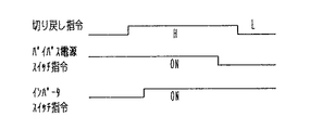
FIG. 19 is a configuration diagram showing a power conversion device according to
In the sixth embodiment, when switching back from the
[0046]
FIG. 20 shows the internal circuit configuration of the
FIG. 21 is a timing chart showing the relationship between the switchback command, the ON / OFF command of the
[0047]
Next, the operation of the seventh embodiment will be described with reference to the timing chart of FIG. First, the
[0048]
In each of the above-described embodiments, a case has been described in which an inverter having a DC voltage source as an input is applied as an AC voltage source. However, if an AC voltage can be output according to a voltage command, for example, a cycloconverter or the like may be used. Even if an AC voltage source of the type is applied, the present invention has the same effect as described above.
[0049]
【The invention's effect】
As described above, the power conversion device of the present invention includes an AC voltage source capable of outputting an AC voltage in response to a voltage command, a first opening / closing unit that connects and disconnects the AC voltage source and a load, a bypass power supply, A second opening / closing means for connecting / disconnecting the bypass power supply to / from the load; and operating the first and second opening / closing means to connect a power supply connected to the load to the AC voltage source and the bypass. In a power converter that supplies power to the load by switching to one of a power supply and
A switching command generating circuit for generating a switching command of the power supply, wherein the AC voltage source and the bypass power supply are three-phase power supplies; and a switching permission when a voltage difference between the AC voltage source and the bypass power supply is within a predetermined range. A switching determination circuit that outputs a signal, and a switching control circuit that receives the switching command and the switching permission signal to open and close the first and second opening / closing means. A subtractor for calculating an instantaneous voltage difference between the AC voltage source and the bypass power supply for each phase, an adder for adding an absolute value of an output of each of the subtractors, and an output of the adder is within a predetermined value. When there is a comparator that outputs the switching permission signal,Even during asynchronous operation without synchronous control, it is possible to switch between power supplies by detecting instantaneous voltage coincidence.Thus, in the case of a three-phase power supply, it is possible to reliably detect the coincidence of the voltages of the two power supplies and to smoothly switch between the power supplies.
[0050]
Also, the power converter of the present inventionAn AC voltage source capable of outputting an AC voltage in response to a voltage command, first switching means for connecting and disconnecting the AC voltage source to and from the load, a bypass power supply, and a second power supply for connecting and disconnecting the bypass power supply to and from the load. Operating the first and second opening / closing means to connect the power supply connected to the load to the AC voltage source and the bypass power supply. A power converter that supplies power to the load by switching to any one of
The AC voltage source and the bypass power source are three-phase power sources, a switching command generating circuit for generating a power source switching command, and an amplitude difference and a phase difference between a voltage of the AC voltage source and a voltage of the bypass power source are within predetermined ranges. A switching determination circuit that outputs a switching permission signal when the switching is within the range, and a switching control circuit that inputs the switching command and the switching permission signal to open and close the first and second opening / closing means. A determining circuit configured to convert the three-phase voltage of the AC voltage source into two phases of a d-axis and a q-axis, and to convert the three-phase voltage of the bypass power supply into two phases of a d-axis and a q-axis; A second 3/2 conversion circuit for conversion, a first subtractor for calculating an instantaneous value difference between d-axis components of outputs of the both 3/2 conversion circuits, and a q-axis of output of the both 3/2 conversion circuits A second subtractor for calculating the instantaneous value difference between the components, An amplitude detection circuit that calculates the square root of the sum of squares of the force; and a comparator that outputs the switching permission signal when the output of the amplitude detection circuit falls within a predetermined value. The problem that the voltage half-wave of the polarity is continuously supplied to the load is eliminated, and in the case of the three-phase power supply, the coincidence of the amplitude and the phase of the two power supplies is reliably detected, thereby enabling the smooth switching between the power supplies. .
[0051]
Further, in the power conversion device according to the present invention, when a switching command for switching the power supply connected to the load from the AC voltage source to the bypass power supply is output, an amplitude difference between the voltage of the AC voltage source and the voltage of the bypass power supply is obtained. Since an adder for adding the output of the first subtractor to the voltage command of the AC voltage source is provided, the shock at the time of switching can be reduced even when the voltage difference between the two power supplies is large.
[0052]
Also, the power conversion device of the present invention includes a storage circuit that stores a voltage output immediately before the stop when the output is stopped due to a failure of the AC voltage source, and the switching determination circuit is configured to switch the voltage stored in the storage circuit. The switching enable signal is output when the amplitude difference and the phase difference between the voltage of the AC power supply and the voltage of the bypass power supply are within the predetermined range. Does not occur, the load does not suffer from a trouble phenomenon such as magnetic bias.
[0053]
Further, the power conversion device of the present invention includes a synchronization control circuit that matches the voltage command of the AC voltage source with the voltage of the bypass power supply and synchronizes the voltages of the two power supplies within a predetermined voltage and frequency range. When a switching command for switching the power supply to be connected from the AC voltage source to the bypass power source is output, and when the synchronization is established, the AC voltage is applied during opening and closing operations of the first and second opening / closing means related to the switching. Since the output of the AC voltage source is maintained and the output of the AC voltage source is stopped simultaneously with the closing operation of the second opening / closing means related to the switching when the synchronization is not established, the output is not reliable. Lap switching can be performed with high reliability, and non-instantaneous interruption switching without voltage deviation can be performed even during asynchronous operation.
[0054]
Also, the power converter of the present inventionAn AC voltage source capable of outputting an AC voltage in response to a voltage command, first switching means for connecting and disconnecting the AC voltage source to and from the load, a bypass power supply, and a second power supply for connecting and disconnecting the bypass power supply to and from the load. By operating the first and second opening / closing means, the power supply connected to the load is switched to one of the AC voltage source and the bypass power supply to supply power to the load. In the power converter to supply,
A switching command generation circuit for generating a switching command for the power supply, a switching determination circuit for detecting a voltage difference between the AC voltage source and the bypass power supply, and outputting a switching permission signal when the voltage difference falls within a predetermined range; A switching control circuit for inputting the switching command and the switching permission signal to open and close the first and second opening / closing means, and a voltage command of the AC voltage source within a predetermined voltage and frequency range. A synchronization control circuit that matches the voltage of the bypass power supply and synchronizes the voltages of the two power supplies; and when a switching command for switching the power supply connected to the load from the AC voltage source to the bypass power supply is output, the synchronization is established. The output of the AC voltage source is maintained during the opening and closing operation of the first and second opening / closing means related to the switching, and the synchronization is not established. At the time, the output of the AC voltage source is stopped at the same time as the closing operation of the second opening / closing means related to the switching, so that even when the synchronous control is not performed, the instantaneous voltage coincidence is detected. Thus, switching between power supplies can be performed, lap switching with high reliability can be performed during synchronization, and instantaneous interruption switching without voltage deviation can be performed even during asynchronous operation.
[0055]
Also, the power converter of the present inventionAn AC voltage source capable of outputting an AC voltage in response to a voltage command, first switching means for connecting and disconnecting the AC voltage source to and from the load, a bypass power supply, and a second power supply for connecting and disconnecting the bypass power supply to and from the load. By operating the first and second opening / closing means, the power supply connected to the load is switched to one of the AC voltage source and the bypass power supply to supply power to the load. In the power converter to supply,
A switching command generation circuit for generating a switching command for the power supply, a switching determination circuit for detecting a voltage difference between the AC voltage source and the bypass power supply, and outputting a switching permission signal when the voltage difference falls within a predetermined range; A switching control circuit for inputting the switching command and the switching permission signal to open and close the first and second opening / closing means; and for bypassing the voltage command of the AC voltage source within a predetermined voltage and frequency range. A synchronization control circuit that matches the voltage of the power supply and synchronizes the voltages of the two power supplies, and a power supply connected to a load when the power supply is switched from the AC voltage source to the bypass power supply and when the power supply is switched from the bypass power supply to the AC voltage source. A range switching circuit is provided for switching the setting of a predetermined voltage and frequency range, so that even when the synchronous control is not performed, the instantaneous voltage coincidence is detected. Switching Minamotoma can and will, also synchronization control when, even if the voltage or frequency of the bypass supply a reliable switching can be performed to the AC voltage source according to the even synchronization control if you vary greatly.
[0056]
In addition, the power converter of the present invention is connected to a synchronous control circuit that matches the voltage command of the AC voltage source with the voltage of the bypass power supply and synchronizes the voltages of the two power supplies within a predetermined voltage and frequency range, and a load connected to the load. A range switching circuit for switching the setting of the predetermined voltage and frequency range between when the power supply to be switched from the AC voltage source to the bypass power supply and when the power supply is switched from the bypass power supply to the AC voltage source. Even when the voltage or frequency of the power supply fluctuates greatly, it is possible to reliably switch to the AC voltage source by the synchronous control.
[Brief description of the drawings]
FIG. 1 is a configuration diagram showing a power conversion device according to
FIG. 2 is an internal circuit configuration diagram of a switching determination circuit of FIG. 1;
3 is an internal circuit configuration diagram of an example different from FIG. 2 of the switching determination circuit of FIG. 1;
FIG. 4 is a timing chart illustrating a switching operation of the power conversion device of FIG.
FIG. 5 is an internal circuit configuration diagram showing a switching determination circuit of the power conversion device according to
FIG. 6 is a diagram showing an allowable voltage deviation range of the switching determination circuit of FIG. 5;
FIG. 7 is a configuration diagram showing a power conversion device according to
FIG. 8 is an internal circuit configuration diagram of the switching determination circuit of FIG. 7;
FIG. 9 is an internal circuit configuration diagram of the voltage command generation circuit of FIG. 7;
FIG. 10 is a timing chart illustrating a switching operation of the power conversion device of FIG. 7;
FIG. 11 is a configuration diagram showing a power conversion device according to
12 is a timing chart illustrating a switching operation of the power conversion device of FIG.
FIG. 13 is a configuration diagram showing a power conversion device according to a fifth embodiment of the present invention.
14 is an internal circuit configuration diagram of the switching determination circuit of FIG.
FIG. 15 is a diagram showing a load voltage waveform at the time of switching of the power converter of FIG.
FIG. 16 is a configuration diagram showing a power conversion device according to
17 is an internal circuit configuration diagram of the frequency tracking range command generation circuit of FIG.
18 is a timing chart illustrating a switching operation of the power conversion device in FIG.
FIG. 19 is a configuration diagram showing a power converter according to
FIG. 20 is an internal circuit configuration diagram of the command switching circuit of FIG. 19;
FIG. 21 is a timing chart illustrating the switching operation of FIG.
FIG. 22 is a configuration diagram showing a conventional power converter.
FIG. 23 is a timing chart illustrating a switching operation of the power conversion device of FIG. 22.
[Explanation of symbols]
2 inverters, 4 inverter switches, 5 bypass switches,
6 bypass power supply, 7 load, 20, 21 voltage sensor,
22 switching command generation circuit, 23 switching control circuit,
25, 25a, 25b synchronization control circuit, 26 voltage amplitude command generation circuit,
27, 27a voltage command generation circuit, 28 voltage control circuit, 29 drive circuit,
30, 30a, 30b, 30c, 30d, 30e switching determination circuit,
31 inverter drive switching circuit, 32 voltage abnormality detection circuit, 33 OR circuit,
34 frequency tracking range command generation circuit, 35 command switching circuit,
100, 102 to 104, 109, 110 subtractor, 105 adder,
106, 112 comparator, 107, 108, 3/2 conversion circuit,
111 amplitude detection circuit, 115, 121, 122 selector.
Claims (8)
上記交流電圧源および上記バイパス電源が三相電源であり、上記電源の切換指令を発生する切換指令発生回路、上記交流電圧源とバイパス電源との電圧差が所定の範囲内になったとき切換許可信号を出力する切換判定回路、および上記切換指令と上記切換許可信号とを入力して上記第1および第2の開閉手段を開閉操作する切換制御回路を備え、上記切換判定回路は、三相各相毎に上記交流電圧源とバイパス電源との瞬時電圧差を演算する減算器、これら各減算器の出力の絶対値を加算する加算器、およびこの加算器の出力が所定の値内になったとき上記切換許可信号を出力する比較器を有することを特徴とする電力変換装置。 A switching command generating circuit for generating a switching command of the power supply, wherein the AC voltage source and the bypass power supply are three-phase power supplies; and a switching permission when a voltage difference between the AC voltage source and the bypass power supply is within a predetermined range. A switching determination circuit that outputs a signal, and a switching control circuit that receives the switching command and the switching permission signal to open and close the first and second opening / closing means. A subtractor for calculating an instantaneous voltage difference between the AC voltage source and the bypass power supply for each phase, an adder for adding an absolute value of an output of each of the subtractors, and an output of the adder is within a predetermined value. A power conversion device for outputting the switching permission signal.
上記交流電圧源および上記バイパス電源が三相電源であり、上記電源の切換指令を発生する切換指令発生回路、上記交流電圧源の電圧とバイパス電源の電圧との振幅差および位相差が所定の範囲内になったとき切換許可信号を出力する切換判定回路、および上記切換指令と上記切換許可信号とを入力して上記第1および第2の開閉手段を開閉操作する切換制御回路を備え、上記切換判定回路は、上記交流電圧源の三相電圧をd軸とq軸の二相に変換する第1の3/2変換回路、上記バイパス電源の三相電圧をd軸とq軸の二相に変換する第2の3/2変換回路、上記両3/2変換回路の出力のd軸成分同士の瞬時値差を演算する第1の減算器、上記両3/2変換回路の出力のq軸成分同士の瞬時値差を演算する第2の減算器、上記両減算器の出力の2乗和の平方根を演算する振幅検出回路、およびこの振幅検出回路の出力が所定の値内になったとき上記切換許可信号を出力する比較器を有することを特徴とする電力変換装置。 The AC voltage source and the bypass power source are three-phase power sources, a switching command generating circuit for generating a power source switching command, and an amplitude difference and a phase difference between a voltage of the AC voltage source and a voltage of the bypass power source are within predetermined ranges. A switching determination circuit for outputting a switching permission signal when the switch is within the range, and a switching control circuit for inputting the switching command and the switching permission signal to open and close the first and second opening / closing means. A determining circuit configured to convert the three-phase voltage of the AC voltage source into two phases of a d-axis and a q-axis, and to convert the three-phase voltage of the bypass power supply into two phases of a d-axis and a q-axis; A second 3/2 conversion circuit for conversion, a first subtractor for calculating an instantaneous value difference between d-axis components of outputs of the both 3/2 conversion circuits, and a q-axis of output of the both 3/2 conversion circuits A second subtractor for calculating the instantaneous value difference between the components, Amplitude detection circuit, and a power converter with an output of the amplitude detection circuit and having a comparator for outputting the switching 換許 enable signal when it is within a predetermined value for calculating the root-sum-square force.
上記電源の切換指令を発生する切換指令発生回路、上記交流電圧源とバイパス電源との電圧差を検出し、この電圧差が所定の範囲内になったとき切換許可信号を出力する切換判定回路、上記切換指令と上記切換許可信号とを入力して上記第1および第2の開閉手段を開閉操作する切換制御回路、および所定の電圧および周波数の範囲内で、上記交流電圧源の電圧指令を上記バイパス電源の電圧に一致させ上記両電源の電圧を同期させる同期制御回路を備え、負荷に接続する電源を、上記交流電圧源からバイパス電源に切り換える切換指令が出力された場合、上記同期が成立しているときは上記切換に係る第1および第2の開閉手段の開閉操作中上記交流電圧源の出力を維持し、上記同期が成立していない非同期時は上記切換に係る上記第2の開閉手段の閉動作と同時に上記交流電圧源の出力を停止するようにしたことを特徴とする電力変換装置。 A switching command generation circuit for generating a switching command for the power supply, a switching determination circuit for detecting a voltage difference between the AC voltage source and the bypass power supply, and outputting a switching permission signal when the voltage difference falls within a predetermined range; A switching control circuit for inputting the switching command and the switching permission signal to open and close the first and second opening / closing means, and a voltage command of the AC voltage source within a predetermined voltage and frequency range. A synchronization control circuit that matches the voltage of the bypass power supply and synchronizes the voltages of the two power supplies; and when a switching command for switching the power supply connected to the load from the AC voltage source to the bypass power supply is output, the synchronization is established. The output of the AC voltage source is maintained during the opening / closing operation of the first and second opening / closing means related to the switching, and when the synchronization is not established, the second voltage related to the switching is maintained. Power conversion device is characterized in that so as to stop the output of the closing operation with the AC voltage source at the same time the closing means.
上記電源の切換指令を発生する切換指令発生回路、上記交流電圧源とバイパス電源との電圧差を検出し、この電圧差が所定の範囲内になったとき切換許可信号を出力する切換判定回路、上記切換指令と上記切換許可信号とを入力して上記第1および第2の開閉手段を開閉操作する切換制御回路、所定の電圧および周波数の範囲内で、上記交流電圧源の電圧指令を上記バイパス電源の電圧に一致させ上記両電源の電圧を同期させる同期制御回路、および負荷に接続する電源を、上記交流電圧源からバイパス電源に切り換えるときと上記バイパス電源から交流電圧源に切り換えるときとで上記所定の電圧および周波数の範囲の設定を切り換える範囲切換回路を備えたことを特徴とする電力変換装置。 A switching command generation circuit for generating a switching command for the power supply, a switching determination circuit for detecting a voltage difference between the AC voltage source and the bypass power supply, and outputting a switching permission signal when the voltage difference falls within a predetermined range; A switching control circuit for inputting the switching command and the switching permission signal to open and close the first and second opening / closing means; and for bypassing the voltage command of the AC voltage source within a predetermined voltage and frequency range. A synchronization control circuit that matches the voltage of the power supply and synchronizes the voltages of the two power supplies, and a power supply connected to a load when the power supply is switched from the AC voltage source to the bypass power supply and when the power supply is switched from the bypass power supply to the AC voltage source. A power converter comprising a range switching circuit for switching a setting of a predetermined voltage and frequency range.
Priority Applications (1)
| Application Number | Priority Date | Filing Date | Title |
|---|---|---|---|
| JP17616998A JP3550573B2 (en) | 1998-06-23 | 1998-06-23 | Power converter |
Applications Claiming Priority (1)
| Application Number | Priority Date | Filing Date | Title |
|---|---|---|---|
| JP17616998A JP3550573B2 (en) | 1998-06-23 | 1998-06-23 | Power converter |
Publications (2)
| Publication Number | Publication Date |
|---|---|
| JP2000014041A JP2000014041A (en) | 2000-01-14 |
| JP3550573B2 true JP3550573B2 (en) | 2004-08-04 |
Family
ID=16008878
Family Applications (1)
| Application Number | Title | Priority Date | Filing Date |
|---|---|---|---|
| JP17616998A Expired - Fee Related JP3550573B2 (en) | 1998-06-23 | 1998-06-23 | Power converter |
Country Status (1)
| Country | Link |
|---|---|
| JP (1) | JP3550573B2 (en) |
Families Citing this family (5)
| Publication number | Priority date | Publication date | Assignee | Title |
|---|---|---|---|---|
| JP4761367B2 (en) * | 2006-02-21 | 2011-08-31 | 東芝三菱電機産業システム株式会社 | Uninterruptible power system |
| JP4586770B2 (en) * | 2006-06-15 | 2010-11-24 | 株式会社明電舎 | Standby uninterruptible power supply system |
| JP5190683B2 (en) * | 2008-06-11 | 2013-04-24 | サンケン電気株式会社 | AC power supply |
| JP6435715B2 (en) * | 2014-08-28 | 2018-12-12 | サンケン電気株式会社 | Uninterruptible power system |
| JP6480522B2 (en) * | 2016-07-28 | 2019-03-13 | 株式会社日立製作所 | Method and system for synchronizing the phase of electrical signals in an uninterruptible power system |
-
1998
- 1998-06-23 JP JP17616998A patent/JP3550573B2/en not_active Expired - Fee Related
Also Published As
| Publication number | Publication date |
|---|---|
| JP2000014041A (en) | 2000-01-14 |
Similar Documents
| Publication | Publication Date | Title |
|---|---|---|
| JP2002142464A (en) | Method of connecting auxiliary power source to power grid and synchronizing it | |
| US6556459B2 (en) | Uninterruptible power supply and method of turning off AC switch for uninterruptible power supply | |
| JP2575500B2 (en) | Three-phase converter | |
| US6862163B2 (en) | Method and device for bridging brief power outages in a matrix converter | |
| US6657319B2 (en) | Electric power system interconnection device | |
| JP2828863B2 (en) | Unbalance compensator for 3-phase / 2-phase converter | |
| JP3992679B2 (en) | Power converter | |
| JP3550573B2 (en) | Power converter | |
| JPH09247952A (en) | Uninterrupted operation method and uninterrupted power supply apparatus | |
| US20190260228A1 (en) | Apparatus and methods to reduce current transient during power mode transfer in uninterruptible power supply | |
| JP4374605B2 (en) | PWM cycloconverter | |
| JP3431504B2 (en) | Inverter device, inverter control device and inverter system | |
| JP6939465B2 (en) | Power converter | |
| JP3167534B2 (en) | Uninterruptible power system | |
| JPH0956170A (en) | Controller for inverter for system linkage | |
| KR102350938B1 (en) | Phase locking device of uninterruptible power supply | |
| JP7310766B2 (en) | power conversion system | |
| JP3217435B2 (en) | Commercial Synchronous Parallel System | |
| JP3115115B2 (en) | Self-excited inverter | |
| WO2023243091A1 (en) | Phase synchronization control circuit and electric power conversion device using same | |
| JPS6318967A (en) | Controller for cycloconverter | |
| JPS63206165A (en) | Uninterruptible power supply | |
| KR102153071B1 (en) | Apparatus for Converting Three Phase Power Independent Phase Rotation Direction | |
| JP3553180B2 (en) | Converter device | |
| JP2001197683A (en) | Uninterruptible power supply apparatus |
Legal Events
| Date | Code | Title | Description |
|---|---|---|---|
| A131 | Notification of reasons for refusal |
Free format text: JAPANESE INTERMEDIATE CODE: A131 Effective date: 20031216 |
|
| A521 | Written amendment |
Free format text: JAPANESE INTERMEDIATE CODE: A523 Effective date: 20040213 |
|
| TRDD | Decision of grant or rejection written | ||
| A711 | Notification of change in applicant |
Free format text: JAPANESE INTERMEDIATE CODE: A712 Effective date: 20040315 |
|
| A01 | Written decision to grant a patent or to grant a registration (utility model) |
Free format text: JAPANESE INTERMEDIATE CODE: A01 Effective date: 20040316 |
|
| A61 | First payment of annual fees (during grant procedure) |
Free format text: JAPANESE INTERMEDIATE CODE: A61 Effective date: 20040317 |
|
| R150 | Certificate of patent or registration of utility model |
Free format text: JAPANESE INTERMEDIATE CODE: R150 |
|
| FPAY | Renewal fee payment (event date is renewal date of database) |
Free format text: PAYMENT UNTIL: 20080514 Year of fee payment: 4 |
|
| FPAY | Renewal fee payment (event date is renewal date of database) |
Free format text: PAYMENT UNTIL: 20090514 Year of fee payment: 5 |
|
| FPAY | Renewal fee payment (event date is renewal date of database) |
Free format text: PAYMENT UNTIL: 20100514 Year of fee payment: 6 |
|
| FPAY | Renewal fee payment (event date is renewal date of database) |
Free format text: PAYMENT UNTIL: 20110514 Year of fee payment: 7 |
|
| FPAY | Renewal fee payment (event date is renewal date of database) |
Free format text: PAYMENT UNTIL: 20110514 Year of fee payment: 7 |
|
| FPAY | Renewal fee payment (event date is renewal date of database) |
Free format text: PAYMENT UNTIL: 20120514 Year of fee payment: 8 |
|
| FPAY | Renewal fee payment (event date is renewal date of database) |
Free format text: PAYMENT UNTIL: 20130514 Year of fee payment: 9 |
|
| FPAY | Renewal fee payment (event date is renewal date of database) |
Free format text: PAYMENT UNTIL: 20140514 Year of fee payment: 10 |
|
| R250 | Receipt of annual fees |
Free format text: JAPANESE INTERMEDIATE CODE: R250 |
|
| R250 | Receipt of annual fees |
Free format text: JAPANESE INTERMEDIATE CODE: R250 |
|
| LAPS | Cancellation because of no payment of annual fees |