JP3204112U - Electronic components - Google Patents
Electronic components Download PDFInfo
- Publication number
- JP3204112U JP3204112U JP2016000862U JP2016000862U JP3204112U JP 3204112 U JP3204112 U JP 3204112U JP 2016000862 U JP2016000862 U JP 2016000862U JP 2016000862 U JP2016000862 U JP 2016000862U JP 3204112 U JP3204112 U JP 3204112U
- Authority
- JP
- Japan
- Prior art keywords
- inductive component
- component according
- component
- inductance
- wire
- Prior art date
- Legal status (The legal status is an assumption and is not a legal conclusion. Google has not performed a legal analysis and makes no representation as to the accuracy of the status listed.)
- Active
Links
- 230000001939 inductive effect Effects 0.000 claims abstract description 68
- 239000006260 foam Substances 0.000 claims abstract description 13
- 239000000463 material Substances 0.000 claims description 16
- 229910000859 α-Fe Inorganic materials 0.000 claims description 14
- 239000000696 magnetic material Substances 0.000 claims description 11
- 210000000988 bone and bone Anatomy 0.000 claims description 5
- 230000001747 exhibiting effect Effects 0.000 claims 9
- 238000001465 metallisation Methods 0.000 abstract description 4
- 239000011162 core material Substances 0.000 description 43
- 238000000034 method Methods 0.000 description 9
- 238000004804 winding Methods 0.000 description 9
- 239000000919 ceramic Substances 0.000 description 7
- 238000005549 size reduction Methods 0.000 description 6
- 229910000679 solder Inorganic materials 0.000 description 5
- 230000008901 benefit Effects 0.000 description 3
- 239000004020 conductor Substances 0.000 description 3
- 230000035699 permeability Effects 0.000 description 3
- NIXOWILDQLNWCW-UHFFFAOYSA-N acrylic acid group Chemical group C(C=C)(=O)O NIXOWILDQLNWCW-UHFFFAOYSA-N 0.000 description 2
- 238000005516 engineering process Methods 0.000 description 2
- 230000004907 flux Effects 0.000 description 2
- 230000006872 improvement Effects 0.000 description 2
- 238000012986 modification Methods 0.000 description 2
- 230000004048 modification Effects 0.000 description 2
- RYGMFSIKBFXOCR-UHFFFAOYSA-N Copper Chemical compound [Cu] RYGMFSIKBFXOCR-UHFFFAOYSA-N 0.000 description 1
- 239000000853 adhesive Substances 0.000 description 1
- 230000001070 adhesive effect Effects 0.000 description 1
- 238000013459 approach Methods 0.000 description 1
- -1 but not limited to Substances 0.000 description 1
- 238000005266 casting Methods 0.000 description 1
- 230000008859 change Effects 0.000 description 1
- 239000011248 coating agent Substances 0.000 description 1
- 238000000576 coating method Methods 0.000 description 1
- 238000000748 compression moulding Methods 0.000 description 1
- 238000010276 construction Methods 0.000 description 1
- 238000007796 conventional method Methods 0.000 description 1
- 229910052802 copper Inorganic materials 0.000 description 1
- 239000010949 copper Substances 0.000 description 1
- 238000013461 design Methods 0.000 description 1
- 238000001746 injection moulding Methods 0.000 description 1
- 239000002184 metal Substances 0.000 description 1
- 229910052751 metal Inorganic materials 0.000 description 1
- 238000004806 packaging method and process Methods 0.000 description 1
- 229920000642 polymer Polymers 0.000 description 1
- 230000008569 process Effects 0.000 description 1
- 230000009467 reduction Effects 0.000 description 1
- 239000002356 single layer Substances 0.000 description 1
- 238000005476 soldering Methods 0.000 description 1
- 239000007787 solid Substances 0.000 description 1
- 238000001228 spectrum Methods 0.000 description 1
- 238000012360 testing method Methods 0.000 description 1
- 238000003466 welding Methods 0.000 description 1
Images


Classifications
-
- H—ELECTRICITY
- H01—ELECTRIC ELEMENTS
- H01F—MAGNETS; INDUCTANCES; TRANSFORMERS; SELECTION OF MATERIALS FOR THEIR MAGNETIC PROPERTIES
- H01F27/00—Details of transformers or inductances, in general
- H01F27/28—Coils; Windings; Conductive connections
- H01F27/29—Terminals; Tapping arrangements for signal inductances
- H01F27/292—Surface mounted devices
-
- H—ELECTRICITY
- H01—ELECTRIC ELEMENTS
- H01F—MAGNETS; INDUCTANCES; TRANSFORMERS; SELECTION OF MATERIALS FOR THEIR MAGNETIC PROPERTIES
- H01F17/00—Fixed inductances of the signal type
- H01F17/04—Fixed inductances of the signal type with magnetic core
-
- H—ELECTRICITY
- H01—ELECTRIC ELEMENTS
- H01F—MAGNETS; INDUCTANCES; TRANSFORMERS; SELECTION OF MATERIALS FOR THEIR MAGNETIC PROPERTIES
- H01F27/00—Details of transformers or inductances, in general
- H01F27/24—Magnetic cores
-
- H—ELECTRICITY
- H01—ELECTRIC ELEMENTS
- H01F—MAGNETS; INDUCTANCES; TRANSFORMERS; SELECTION OF MATERIALS FOR THEIR MAGNETIC PROPERTIES
- H01F27/00—Details of transformers or inductances, in general
- H01F27/28—Coils; Windings; Conductive connections
- H01F27/2823—Wires
- H01F27/2828—Construction of conductive connections, of leads
-
- H—ELECTRICITY
- H01—ELECTRIC ELEMENTS
- H01F—MAGNETS; INDUCTANCES; TRANSFORMERS; SELECTION OF MATERIALS FOR THEIR MAGNETIC PROPERTIES
- H01F41/00—Apparatus or processes specially adapted for manufacturing or assembling magnets, inductances or transformers; Apparatus or processes specially adapted for manufacturing materials characterised by their magnetic properties
- H01F41/02—Apparatus or processes specially adapted for manufacturing or assembling magnets, inductances or transformers; Apparatus or processes specially adapted for manufacturing materials characterised by their magnetic properties for manufacturing cores, coils, or magnets
- H01F41/04—Apparatus or processes specially adapted for manufacturing or assembling magnets, inductances or transformers; Apparatus or processes specially adapted for manufacturing materials characterised by their magnetic properties for manufacturing cores, coils, or magnets for manufacturing coils
- H01F41/06—Coil winding
- H01F41/076—Forming taps or terminals while winding, e.g. by wrapping or soldering the wire onto pins, or by directly forming terminals from the wire
-
- H—ELECTRICITY
- H01—ELECTRIC ELEMENTS
- H01F—MAGNETS; INDUCTANCES; TRANSFORMERS; SELECTION OF MATERIALS FOR THEIR MAGNETIC PROPERTIES
- H01F3/00—Cores, Yokes, or armatures
- H01F3/10—Composite arrangements of magnetic circuits
Abstract
【課題】縮小されたサイズの表面実装可能な表面実装誘導性構成部品を提供する。【解決手段】表面実装可能な誘導性構成部品10は、主水平部分12c、およびそこから延びるサポートを有する小型チップフォームと、チップフォームをプリント回路板に電気的に接続するためにサポート20、22に接続された金属化パッド28、30と、チップフォームの主水平部分12cの少なくとも一部分の周りに巻かれ、それぞれの金属化パッド28、30に接続される第1の端部12a、32aおよび第2の端部12b、32bを有するワイヤ32とを含む。誘導性構成部品は、約2.1から約2.5の範囲内の長さ対幅比を有する。【選択図】図1A surface mount inductive component capable of surface mounting of reduced size is provided. A surface mountable inductive component 10 includes a small chip form having a main horizontal portion 12c and a support extending therefrom, and supports 20, 22 for electrically connecting the chip form to a printed circuit board. And the first ends 12a, 32a and the first ends 12a, 32a wound around at least a portion of the main horizontal portion 12c of the chip foam and connected to the respective metallization pads 28, 30. A wire 32 having two end portions 12b and 32b. The inductive component has a length to width ratio in the range of about 2.1 to about 2.5. [Selection] Figure 1
Description
本開示は、一般に電子構成部品に関する。より詳細には、本開示は、より大きい構成部品と比較可能に機能する縮小されたサイズを有する縮小されたサイズの表面実装可能な誘導性構成部品、および関連の方法に関する。 The present disclosure relates generally to electronic components. More particularly, the present disclosure relates to a reduced size surface mountable inductive component having a reduced size that functions comparably with a larger component, and related methods.
エレクトロニクス産業は、より小さくより強力な製品を作ることを継続的に目指している。モバイルエレクトロニクスデバイス(たとえば、スマートフォン)、ポータブルコンピュータ、コンピュータアクセサリ、手持ち式エレクトロニクスなどの製品は、より小さな電子構成部品に対する需要を生み出す。これらの製品は、エレクトロニクスの小型化に関して新しいエリアおよびアイデアを調査するための技術をさらに推進する。 The electronics industry is continuously aiming to make smaller and more powerful products. Products such as mobile electronics devices (eg, smartphones), portable computers, computer accessories, handheld electronics, etc. create a demand for smaller electronic components. These products further promote technology to investigate new areas and ideas regarding electronics miniaturization.
電子回路は、主にプリント回路板(PCB)上で使用される構成部品のサイズによって制限される。すなわち、電子構成部品が小さくされれば、それらの回路もまた小さくされ得る。残念ながら、性能または構造的な完全性など価値のあるものを犠牲にすることなしにいくつかの電子構成部品のサイズを縮小することは困難となり得る。なぜなら、より小さな部品を使用するとき、構成部品に所望のパラメータが達成され得ないからである。 Electronic circuits are limited primarily by the size of the components used on the printed circuit board (PCB). That is, if electronic components are made smaller, their circuits can also be made smaller. Unfortunately, it can be difficult to reduce the size of some electronic components without sacrificing something valuable such as performance or structural integrity. This is because when using smaller parts, the desired parameters cannot be achieved for the component.
誘導性構成部品は、これらの誘導性構成部品に使用される部品のサイズが多数の性能パラメータに容易に影響を及ぼし得るため、このサイズ/性能の兼ね合いをよく示す。たとえば、ワイヤゲージ(ワイヤの直径)は、DC抵抗(DCR)、自己共振周波数(SRF)、および/または誘導性構成部品の電流搬送能力に影響を及ぼす可能性がある。すなわち、一般に、より小さい、またはより細いワイヤは、より高い抵抗を有し、したがってインダクタの有効性を制限する。したがって、より細いゲージのワイヤはより小さい構成部品の構築を可能にするが、それらのより小さい構成部品は、その構成部品の元のより大きいバージョンと比較可能に(たとえば、比較可能なインダクタンス、周波数範囲、Q値、自己共振周波数などで)機能することができない可能性がある。 Inductive components show this size / performance trade-off well because the size of the parts used for these inductive components can easily affect a number of performance parameters. For example, wire gauge (wire diameter) can affect DC resistance (DCR), self-resonant frequency (SRF), and / or current carrying capacity of inductive components. That is, generally smaller or thinner wires have higher resistance and thus limit the effectiveness of the inductor. Thus, thinner gauge wires allow the construction of smaller components, but those smaller components are comparable to the original larger version of that component (eg, comparable inductance, frequency May not function (with range, Q value, self-resonant frequency, etc.).
本開示は、表面実装誘導性構成部品、およびそれに関する方法の例について述べる。いくつかの形態では、構成部品は、主水平部分と、そこから延びるサポートとを有する小型チップフォームを含む。構成部品は、チップフォームをプリント回路板に電気的に接続するためにサポートに接続された端子を含む。ワイヤ、特に52〜56ゲージのワイヤが、チップフォームの主水平部分の少なくとも一部分の周りに巻かれ、第1の端部および第2の端部がそれぞれの端子に接続されている。いくつかの形態では、これらの端子は、構成部品の外部表面上に形成された金属化パッドであり、他の形態では、それらは、ワイヤ自体の端部によって形成されても、構成部品に接続されたチップの形状をとってもよい。誘導性構成部品は、約2.1から約2.5の範囲内、より具体的には約2.2から約2.4の範囲内、さらに具体的には約2.4の長さ対幅比を有する。 The present disclosure describes examples of surface mount inductive components and methods related thereto. In some forms, the component includes a miniature chip form having a main horizontal portion and a support extending therefrom. The component includes a terminal connected to the support for electrically connecting the chip form to the printed circuit board. A wire, in particular a 52-56 gauge wire, is wound around at least a portion of the main horizontal portion of the chip foam and the first end and the second end are connected to the respective terminals. In some forms, these terminals are metallized pads formed on the exterior surface of the component; in other forms they are connected to the component even though they are formed by the end of the wire itself. The shape of the chip may be taken. Inductive components have a length pair in the range of about 2.1 to about 2.5, more specifically in the range of about 2.2 to about 2.4, and more specifically about 2.4. Has a width ratio.
本開示は、当技術分野で知られている他のインダクタからサイズが縮小され、一方、既存のインダクタのパフォーマンスケイパビリティおよび/または要件を維持するインダクタについて述べる。驚くべきことに、約2.1から約2.5の範囲内の長さ対幅比を有するインダクタを提供することにより、パフォーマンスケイパビリティ、またはインダクタンス値にわたるSRFまたはDCRなど動作パラメータに著しい影響を及ぼすことなしに、インダクタのサイズを縮小することができることが発見された。いくつかの例では、約2.2から約2.4のより狭い長さ対幅比でさえ、さらに望ましい結果を生むことができる。状況によっては、約2.4の長さ対幅比が、性能パラメータを最適化しながらインダクタのサイズを縮小するのに最適なものとなり得る。他の例では、他の長さ対幅比、たとえば2.33の長さ対幅比が、いくつかの応用例のためにサイズおよび性能を最適化するのに適したものとなり得る。 The present disclosure describes an inductor that is reduced in size from other inductors known in the art while maintaining the performance capabilities and / or requirements of existing inductors. Surprisingly, providing an inductor having a length to width ratio in the range of about 2.1 to about 2.5 has a significant impact on performance capabilities, or operating parameters such as SRF or DCR over inductance values. It has been discovered that the size of the inductor can be reduced without this. In some examples, even narrower length to width ratios of about 2.2 to about 2.4 can produce even more desirable results. In some circumstances, a length to width ratio of about 2.4 may be optimal for reducing the size of the inductor while optimizing performance parameters. In other examples, other length to width ratios, such as a 2.33 length to width ratio, may be suitable for optimizing size and performance for some applications.
図6Aは、当技術分野でCoilcraft(登録商標)0402シリーズチップインダクタとして知られているチップインダクタを示す。このチップインダクタは、1.19mmの長さ、0.635mmの幅、および0.66mmの高さを有する。(注:添付の図面に示されている寸法は、ミリメートルではなくインチである。)さらに、図6Bに示されているように、このチップインダクタは、1.02mmの長さ、0.51mmの幅、および0.51mmの高さを有する犬の骨形またはダンベル形チップフォームを画定するコアおよびサポートを有する。この構成部品は、1〜100nHの間のインダクタンスで、また31〜77(900MHz時)または32〜100(1.7GHz時)の間に及ぶQ値と共に提供され得る。この構成部品の性能パラメータは魅力的であるが、この構成部品のサイズは、そのような構成部品を配置するためのPCB上の空間が制限された密集した回路および/または製品など、いくつかの応用例でそれが使用されることを妨げることがある。 FIG. 6A shows a chip inductor known in the art as a Coilcraft® 0402 series chip inductor. This chip inductor has a length of 1.19 mm, a width of 0.635 mm, and a height of 0.66 mm. (Note: The dimensions shown in the accompanying drawings are inches rather than millimeters.) Further, as shown in FIG. 6B, this chip inductor is 1.02 mm long, 0.51 mm long It has a core and a support that defines a dog bone-shaped or dumbbell-shaped tip foam having a width and a height of 0.51 mm. This component can be provided with an inductance between 1 and 100 nH and with a Q value ranging between 31 and 77 (at 900 MHz) or between 32 and 100 (at 1.7 GHz). Although the performance parameters of this component are attractive, the size of this component is limited to several components, such as dense circuits and / or products with limited space on the PCB for placing such components. Applications may prevent it from being used.
0402シリーズチップインダクタの性能パラメータを維持するために、構成部品は、単にサイズを縮小させることができない。たとえば、構成部品の寸法が単に25%縮小された場合、構成部品は、元の0402シリーズチップインダクタと比較可能なインダクタンス、周波数、Q値、および自己共振周波数値の範囲を提供することができない。特定の例として、構成部品は、0402シリーズチップインダクタの範囲内で指定されたより高いインダクタ値に到達することができない。なぜなら、構成部品の縮小されたサイズにより、ワイヤの巻き数が減少されることになるからである。これらのインダクタンス値に到達できないことは、構成部品を使用することができる応用例の数を減少させ、どんな電気回路で使用するにも構成部品を不十分なものにすることになる。特に、0402シリーズチップの長さ対幅比は、約2.0である。 In order to maintain the performance parameters of the 0402 series chip inductor, the components cannot simply be reduced in size. For example, if the component dimensions are simply reduced by 25%, the component cannot provide a range of inductance, frequency, Q value, and self-resonant frequency values that are comparable to the original 0402 series chip inductor. As a specific example, the component cannot reach the higher inductor value specified within the 0402 series chip inductor. This is because the number of turns of the wire is reduced due to the reduced size of the components. Failure to reach these inductance values reduces the number of applications in which the component can be used, and makes the component inadequate for use in any electrical circuit. In particular, the length to width ratio of the 0402 series chip is about 2.0.
本開示は、前述の限界を克服する改善された電子構成部品を提供し、現在のデバイスで使用可能でない能力、特徴、および機能をさらに提供する。本開示は、0402のものからサイズが縮小され、それによりPCB上でより少ない面積を占有し、一方、依然として同じ、同様の、または同等の性能特性を維持する改善された電子構成部品を提供する。たとえば、本開示は、0402よりも60%(たとえば、65%サイズ縮小またはそれ以上)サイズが縮小され、一方、やはりSRFを増大し、構成部品によって示されるインダクタンス対DCR比を減少させ、これらのそれぞれは、望ましい改善を表す、電子構成部品を提供する。 The present disclosure provides improved electronic components that overcome the aforementioned limitations and further provide capabilities, features, and functions that are not available in current devices. The present disclosure provides an improved electronic component that is reduced in size from that of 0402, thereby occupying less area on the PCB, while still maintaining the same, similar, or equivalent performance characteristics. . For example, the present disclosure reduces the size by 60% (eg, 65% size reduction or more) than 0402, while also increasing the SRF and reducing the inductance to DCR ratio exhibited by the component, Each provides an electronic component that represents the desired improvement.
これらの改善された電子構成部品は、構成部品の長さ対幅比を修正し、その比を、約2から1の値から、約2.1から約2.5の範囲内、より具体的には約2.2から約2.4の範囲内、さらに具体的には約2.4の値に大きくすることによってこれらの望ましい結果を達成する。驚くべきことに、構成部品のこの長さ対幅比を拡大することは、標準的な進歩で達成されるものより大きい比率に構成部品のサイズを縮小することを可能にすることが発見された。たとえば、従来、構成部品は、標準的な改善において約50〜56%だけサイズが縮小する。しかし、ここでは、性能パラメータを低下させることなしに60%を超えるサイズ縮小を達成することができる。さらに、比のこの増大は、驚くべきことに、以前の構成部品(たとえば、0402シリーズチップ)のものより高いSRF値および低いインダクタンス対DCR比を実際に示す構成部品をもたらした。 These improved electronic components modify the length-to-width ratio of the component so that the ratio is more specifically within a range of about 2.1 to about 2.5 from a value of about 2 to 1. These desired results are achieved by increasing to a value in the range of about 2.2 to about 2.4, and more specifically about 2.4. Surprisingly, it has been discovered that increasing this length-to-width ratio of a component allows the component size to be reduced to a ratio greater than that achieved with standard advances. . For example, traditionally, components are reduced in size by about 50-56% in standard improvements. Here, however, a size reduction of more than 60% can be achieved without reducing the performance parameters. Furthermore, this increase in ratio surprisingly resulted in components that actually exhibited higher SRF values and lower inductance to DCR ratios than those of previous components (eg, 0402 series chips).
本明細書に記載の小型電子構成部品の一例は、主水平区間が間に延在する第1の端部および第2の端部を有するコアと、コアを支持するための第1のサポートおよび第2のサポートとを備える。第1のサポートおよび第2のサポートは、細長いコアのそれぞれの第1の端部および第2の端部から延び、コアと共に、チップフォームを画定する。構成部品をプリント回路板(PCB)上の関連のランドに電気的かつ機械的に取り付けるために、金属化パッドなど端子が構成部品に接続され得る。構成部品は、コアの主水平区間の少なくとも一部分の周りに巻かれ、端子の1つにそれぞれ電気的に接続される第1の端部および第2の端部を有するワイヤをさらに含む。しかし、前述のように、代替的形態では、ワイヤの端部は、端子それ自体として使用されても(たとえば、自己リード接続構成部品にする)、クリップタイプの端子が構成部品にクリップ止めされてもよい。 An example of a small electronic component described herein includes a core having a first end and a second end with a main horizontal section extending therebetween, a first support for supporting the core, and Second support. The first support and the second support extend from the respective first and second ends of the elongated core and together with the core define a chip foam. Terminals, such as metallized pads, can be connected to the component to electrically and mechanically attach the component to an associated land on a printed circuit board (PCB). The component further includes a wire having a first end and a second end wound around at least a portion of the main horizontal section of the core and each electrically connected to one of the terminals. However, as described above, in an alternative form, the end of the wire is used as the terminal itself (eg, a self-leading connection component), but the clip-type terminal is clipped to the component. Also good.
一形態では、サポートおよびコアは、長さ、幅、および高さを有するチップフォームを画定する。チップフォームは、犬の骨/ダンベル形またはH字形で提供されてもよい。いくつかの例では、チップは、それだけには限らないが、磁性材料(たとえば、フェライト)、硬磁性材料および軟磁性材料、ならびにセラミックを含めて、様々な材料から形成され得る。いくつかの例では、サポートおよびコアは、セラミックサポートを有するフェライトコアなど、異なる材料製であってもよい。さらに、チップフォームは、約2.1から約2.5の範囲内である長さ対幅比で設計されることが好ましい。 In one form, the support and the core define a chip foam having a length, width, and height. The tip foam may be provided in a dog bone / dumbbell shape or H-shape. In some examples, the chip may be formed from a variety of materials including, but not limited to, magnetic materials (eg, ferrites), hard and soft magnetic materials, and ceramics. In some examples, the support and core may be made of different materials, such as a ferrite core with a ceramic support. Further, the chip foam is preferably designed with a length to width ratio that is in the range of about 2.1 to about 2.5.
ワイヤ巻き線は、コアの少なくとも一部分の周りに巻かれた絶縁ワイヤの単一の層を備え、絶縁ワイヤの各巻き線は、コアの少なくとも一部分と直接接触することが好ましい。ワイヤは、たとえば54ゲージのワイヤとすることができる。他の例は、ワイヤは、52ゲージから56ゲージのワイヤの範囲内とすることができる。代替的形態では、ワイヤは、列をなして巻かれてもよく、ワイヤの1つの列だけがコアと接触する。ここまで丸い絶縁ワイヤについて論じられているが、代替的形態では、フラットワイヤなど他のタイプの導体または導電性材料が使用されてもよいことを理解されたい。 Preferably, the wire winding comprises a single layer of insulated wire wound around at least a portion of the core, and each winding of the insulated wire is in direct contact with at least a portion of the core. The wire can be, for example, a 54 gauge wire. As another example, the wire can be in the range of 52 gauge to 56 gauge wire. In an alternative form, the wires may be wound in rows and only one row of wires is in contact with the core. Although a round insulated wire has been discussed so far, it should be understood that in alternative forms other types of conductors or conductive materials such as flat wires may be used.
いくつかの例では、構成部品は、ワイヤ巻き線の少なくとも一部分を覆うカバーまたは上部部分をも含むことができる。好ましくは、カバーは、業界標準のピックアンドプレース機器を使用して構成部品がピックアンドプレースされ得る概して平坦な上面を有する。一形態では、カバーは、アクリル材料製であり、概して矩形の水平プレート構造を有し、プレートの周囲から壁が延び、ボックスタイプの蓋構造を形成する。しかし、カバーは、非磁性材料(たとえば、セラミックなど)または磁性材料(たとえば、フェライトなど)など代替の材料製であってもよく、構成部品の上部の上に延在する平坦なスラブ、または構成部品の上部および側部の上に延在するハウジングなど、代替的形態を有してもよいことを理解されたい。たとえば、コアおよびカバーは、フェライトなど磁性材料製であり、導電性構成部品と共に使用されたとき構成部品がフェライトの磁気特性を利用することを可能にしてもよい。他の形態では、カバーおよび巻き線は、射出成形プロセスもしくは圧縮成形プロセスを介して、または注型プロセスを介してそのような材料でオーバーモールドされてもよい。そのようなオーバーモールディングは、構成部品のフランジ付き端部の上に形成されなくてもよく、構成部品の全体的な高さを増大することなしにコイルをシールドすることが望ましい場合、コアのワイヤが巻かれた部分だけでもよい。 In some examples, the component can also include a cover or top portion that covers at least a portion of the wire winding. Preferably, the cover has a generally flat top surface on which components can be picked and placed using industry standard pick and place equipment. In one form, the cover is made of acrylic material and has a generally rectangular horizontal plate structure with walls extending from the perimeter of the plate to form a box-type lid structure. However, the cover may be made of an alternative material such as a non-magnetic material (e.g., ceramic) or magnetic material (e.g., ferrite), a flat slab or configuration extending over the top of the component It should be understood that alternative forms may be provided, such as a housing extending over the top and sides of the part. For example, the core and cover may be made of a magnetic material such as ferrite, allowing the component to take advantage of the magnetic properties of the ferrite when used with a conductive component. In other forms, the cover and windings may be overmolded with such materials via an injection molding process or compression molding process, or via a casting process. Such overmolding may not be formed on the flanged end of the component, and if it is desirable to shield the coil without increasing the overall height of the component, the core wire Only the part where is wrapped may be used.
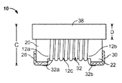
図1および図2A〜図2Dは、本記載の技術による電子構成部品の例を提供する。図1は、薄型の電子構成部品を全体的に符号10で示す。図2A〜Dは、図1に示されているものと本質的に同じ構成部品であるものを示し、上部部分またはカバー38(またはラベルなどピックアンドプレース材料)が、ピックアンドプレース機械など業界標準の構成部品配置機器を使用して構成部品を拾い上げることができる平坦化された表面を提供するために構成部品に接続されているだけである。 1 and 2A-2D provide examples of electronic components according to the techniques described herein. FIG. 1 shows a thin electronic component generally at 10. 2A-D show what are essentially the same components as shown in FIG. 1, where the top portion or cover 38 (or pick and place material such as a label) is an industry standard such as pick and place machinery. It is only connected to the component to provide a flattened surface that can be picked up using the component placement equipment.
これらの実施形態では、構成部品10は、主水平区間12cが間に延在する第1の端部12aおよび第2の端部12bを有する概して矩形形状のコア12を有する薄型のチップインダクタを構成する。コア12の矩形形状は、構成部品10の薄型を維持する助けとなる。たとえば、図の矩形のコアと同じまたは同様の体積の丸いコアは、構成部品に高さを追加することになり、それにより、それを厳しい高さ限界を有する応用例であまり望ましくないものにする。第1のサポート20および第2のサポート22がコア12に接続され、好ましくはそれと一体化される。図1に示されている実施形態では、コア12およびサポート20、22は、セラミックの固体片から形成され得る。
In these embodiments, the
しかし、代替的実施形態では、サポート20、22は、構成部品10を強化する、および/またはサポートとコアが異なる材料から作製されることを可能にするために、別々の構造物であってもよい。たとえば、代替的実施形態では、参照によりその全体が本明細書に組み込まれる2004年2月10日に発行された特許文献1に開示されているように、サポート20、22は、中にフェライトコア12が配設されるセラミックレセプタクルの形態にあってもよい。この設計は、構成部品10がフェライトの磁気特性およびセラミックの構造的強度を利用することを可能にし、それにより、構成部品の磁束密度を増大し、構成部品10が受ける機械的な力を吸収する、および/またはそれに耐えるための構成部品の能力を強化する。あるいは、サポートは、コア12が接続されるベースを形成するように接続されてもよい。たとえば、参照によりその全体が本明細書に組み込まれる2004年4月6日に発行された特許文献2に開示されているように、サポートは、その上にフェライトコアが置かれるセラミックベースを形成してもよい。
However, in alternative embodiments, the
図1および図2A〜Dに示されているように、サポート20、22はまた、はんだを介してPCB上の対応するランドに構成部品を電気的かつ機械的に接続するために使用されるそれぞれの金属化パッド28、30を有する。このようにして、構成部品は、PCB上に位置する回路内に追加され得る。金属化パッド28、30は、金属化パッドとサポートとの間の結合を強化するために、また構成部品とPCB上のランドとの間に生み出されるはんだ接続を強化するために、サポートに接合され、L字形であることが好ましい。より具体的には、L字形金属化パッドは、パッドをサポートに、またパッドをPCBランドに接続する表面積の量を増大する。表面積のこの増大は、構成部品のこれらの部分とPCBとの間のより強力な結合をもたらす。サポート20、22の底面全体を、これらの表面の一部分だけを覆うのではなく、金属化パッド28、30に覆わせることによって、同様の利益が達成される。
As shown in FIGS. 1 and 2A-D, the
代替的実施形態では、金属化パッド28、30は、異なる形状およびサイズで提供されてもよい。たとえば、一形態では、パッドは、サポート20、22の底面および側面の上に延在する概してU字形のパッドであってもよい。そのような構成は、金属化パッド28、30とサポート20、22との間の接続、および構成部品10とPCB上に位置する対応するランドとの間の接続を、構成部品がそこにはんだ付けされた後で、強化することができる。たとえば、パッドの追加の側壁部分は、金属化パッドをサポートに接続する表面積の量を増大し、それにより、パッドとサポートとの間の強度を増大する。同様に、金属化パッドは、PCB上の対応するランドにはんだ付けされ得るより多くの表面積を含み、それにより、これらの2つの物品間の接続の機械的強度を増大する。
In alternative embodiments, the metallized
他の形態では、金属化パッド28、30は、構成部品上に押圧されるクリップのように形成されてもよい。たとえば、パッドは、サポート20、22の端部の上に(たとえば、U字形の場合)、またはコアもしくは構成部品の側部と上部および底部との上に(たとえば、C字形の場合)押圧される概してU字形またはC字形であってよい。より具体的には、クリップは、サポート20、22上に押し嵌めまたは摩擦嵌めされても、接着剤によって固定されても、その両方であってもよい。他の形態では、金属化パッド28、30は、サポート20、22の底面に付着された金属コーティングを単に備えてもよい。さらに他の形態では、ワイヤ端部は、上記で論じたように、端子またははんだパッドを形成してもよい(たとえば、自己リード接続)。
In other forms, the metallized
図1および図2A〜Dに示されているように、電子構成部品10は、コア12の主水平区間18の少なくとも一部分の周りに巻かれたワイヤ32をも含む。図の実施形態では、ワイヤ32は、銅など導電性材料から作製され、構成部品がはんだ付けされたときPCB上の回路に電気的に接続され得るように金属化パッド28、30に電気的に接続される第1の端部32aおよび第2の端部32bを有する。より具体的には、第1の端部32aは、金属化パッド28に接続され、第2の端部32bは、金属化パッド30に接続される。両端部32a〜bは、それぞれが金属化パッド28、30の底部からはみ出す量を最小限に抑えるように平坦化または押圧される。これは、金属化パッド28、30がPCB上の対応するランドから盛り上がることになる量を最小限に抑え、構成部品がPCBにはんだ付けされたときワイヤ端部32a〜bおよびパッド28、30が共にはんだで確実にコーティングされることになるようにする助けとなる。さらに、平坦化された端部32a〜bは、構成部品10がPCB上でよりまっすぐに置かれることを可能にし、構成部品の配置をより容易にする。上記のように、ワイヤ32は、様々なサイズまたは寸法をとることができる。たとえば、一実施形態では、ワイヤ32は、52ゲージから56ゲージのワイヤとすることができる。いくつかの実施形態では、構成部品の構成および形状に応じて、54ゲージのワイヤが最適に機能する縮小されたサイズの構成部品をもたらすことができることが判明している。
As shown in FIGS. 1 and 2A-D, the
図2A〜Dに示されているように、電子構成部品10は、ピックアンドプレース機械など業界標準の構成部品配置機器を使用して構成部品を拾い上げることができる平坦化された表面を提供するために構成部品に接続された上部部分またはカバー38をも有してもよい。そのような上部部分38は、電子構成部品の購入者によって広く使用され好まれるテープおよびリールのパッケージングでパッケージ化されることを可能にする。図の実施形態では、上部部分38は、形状が概して矩形であり、外側側壁がそこから下向きに延びている。そのような構成は、上部部分38が、ワイヤが巻かれたコア12の少なくとも一部分の上、好ましくはコア12、サポート20、22、およびワイヤ32の上でカバーとして動作することを可能にする。チップフォーム全体およびワイヤの上に延在するカバーはまた、電流を搬送するワイヤ32を覆い、それが電流を搬送している間、不注意で触れられることも短絡することもできないようにする追加の保護を提供する。
As shown in FIGS. 2A-D, the
一形態では、上部部分38は、アクリル製であり、真空ピックアンドプレース機器が構成部品をリールから取得および除去し、パッケージ化された構成部品10をPCB上に配置するための大きい、概して平坦な上部表面を提供する。しかし、代替的形態では、上部部分38は、構成部品10の性能をさらに向上させるために、フェライトなど磁性材料製であってもよい。フェライトの上部部分は、参照によりその全体が本明細書に組み込まれている特許文献2でさらに論じられているように、構成部品10のインダクタンスを著しく増大し、その漏れインダクタンスを低減することになる。いくつかの例では、上部部分またはカバー38は、プラスチック(または他のポリマー)ラベルまたは紙ラベルなど、ラベルとして形成され得る。そのような向上された性能が必要とされない他の実施形態では、上部部分38は、プラスチックまたは他の同様の材料から作製されてもよい。
In one form, the
そのような構成部品は、様々な応用例で使用され得、さらに応用例特有の使用のために設計され得る。より具体的には、構成部品の様々な部品(たとえば、コア12、サポート20、22、ワイヤ32、およびカバー38)に使用される実際の材料は、構成部品が使用されることになる特定の応用例のために特に選択されてもよい。たとえば、より敏感なコイル32を必要とする応用例では、より高い透磁率を有するコア材料が使用されることになる。材料の透磁率が高くなるほど、構成部品のインダクタンスが高くなり、より低い周波数で動作しているにもかかわらず、コイルが敏感になる。あるいは、構成部品がより高い周波数で、またはそれほど敏感でないコイルで動作することを応用例が必要とする場合、より低い透磁率値を有する材料が選択されてもよい。
Such components can be used in a variety of applications and can be designed for application specific use. More specifically, the actual material used for the various components of the component (eg,
一形態では、構成部品は、約0.76mm(約0.030インチ)の長さ、約0.33mm(約0.013インチ)の幅、および約0.56mm(約0.022インチ)の高さを有する。本願には、そのような電子構成部品の1つまたは複数の例に関するさらなる仕様および情報を含む製品データシートが添付されている。 In one form, the component has a length of about 0.030 inch, a width of about 0.013 inch, and a width of about 0.022 inch. Has a height. Accompanying this application is a product data sheet containing additional specifications and information regarding one or more examples of such electronic components.
これらの構成は、Coilcraft(登録商標)0402チップインダクタなど、より大きい構成部品によって提供されるものと比較可能な、さらにはそれらより大きいインダクタンスおよびQ値を構成部品が提供することを可能にすることになり、一方、著しく縮小された構成部品サイズを提供する。ワイヤ32の選択されるその寸法、および巻き線の数が、全体的な構成部品性能パラメータを決定することになる。たとえば、ワイヤのより小さな長さ寸法および/またはより圧縮された巻き線は、細長い螺旋コイルではなく、より円形または環状のコイルをワイヤ32に形成させることになる。これは、構成部品の磁束密度を増大することになり、これは、構成部品のインダクタンスおよびリアクタンスを増大させる。より具体的には、構成部品のリアクタンスは、この式によって決定され得る。
These configurations can be compared to those provided by larger components, such as Coilcraft® 0402 chip inductors, and also allow components to provide greater inductance and Q values. While providing a significantly reduced component size. The selected size of the
リアクタンス=2π×周波数×インダクタンス Reactance = 2π × frequency × inductance
したがって、追加の巻き線は、インダクタンスを増大させることになり、次いで構成部品のリアクタンスを増大させる。構成部品のQ値は、この式によって決定され得る。 Thus, the additional winding will increase the inductance, which in turn increases the reactance of the component. The Q value of the component can be determined by this equation.
![]()
![]()
したがって、リアクタンスの増大はまた、構成部品の抵抗が維持される、または低減されることになると仮定して、構成部品のQ値の増大をもたらすことになる。図3〜図5に示されている実施形態では、ワイヤ巻き線の間隔もまた、望むなら、構成部品のインダクタンスをさらに変えるために変更されてもよい。 Thus, an increase in reactance will also result in an increase in the Q value of the component, assuming that the resistance of the component will be maintained or reduced. In the embodiment shown in FIGS. 3-5, the spacing of the wire windings may also be varied to further change the inductance of the component, if desired.
以下は、Coilcraft(登録商標)0402チップインダクタなど、より大きい構成部品と比較可能なインダクタンスおよびQ値を有する構成部品を作り出す実施形態の特定の例について論じる。しかし、これらの実施形態は本発明に従って作製される構成部品の例にすぎず、本発明が当てはまる唯一の実施形態と解釈されるべきでないことを理解されたい。 The following discusses a specific example of an embodiment that creates a component having an inductance and Q value that is comparable to a larger component, such as a Coilcraft® 0402 chip inductor. However, it should be understood that these embodiments are merely examples of components made in accordance with the present invention and should not be construed as the only embodiments to which the present invention applies.
両チップフォームのコア12は、図6A〜Bに示されている犬の骨形またはダンベル形チップフォームを形成するようにサイズが減少するのではなく、サポート20、22と同じ幅を維持する。これは、コアの周囲長および巻き線の直径を増大し、これは、構成部品がより大きい0402チップインダクタコイル構成部品と比較可能に動作することを可能にする。たとえば、0402チップインダクタの断面積は、0.014インチ(0.356mm)(長さ)×0.014インチ(0.356mm)(幅)であり、これは1.96×10⁻⁴平方インチ(0.12645mm2)に等しい。図2Cのコアの断面積は、0.0145インチ(0.368mm)(長さ)×0.020インチ(0.508mm)(幅)であり、これは2.9×10⁻⁴平方インチ(0.1871mm2)に等しい。
The
さらに、この実施形態についての長さ対幅比のアスペクト比は、値1に近づき、0402チップインダクタよりこの理想値に近い。より具体的には、図6A〜Bの0402チップインダクタのアスペクト比は、次式である。 Further, the aspect ratio of the length to width ratio for this embodiment approaches a value of 1 and is closer to this ideal value than the 0402 chip inductor. More specifically, the aspect ratio of the 0402 chip inductor in FIGS.
![]()
![]()
そのようなアスペクト比は、電子構成部品10にとってより良好なQ値を生む。
Such an aspect ratio yields a better Q value for the
この実施形態は、Coilcraft(登録商標)0402チップインダクタと比較可能な、さらにはそれより良好なインダクタンスおよびQ値の範囲を生ずることができるが、チップフォーム全体が縮小されることが可能であり、依然として比較可能なインダクタンスおよびQ値の範囲を生ずる。そのような縮小されたチップフォームの例が図1〜図5に示されている。 This embodiment can produce an inductance and Q value range that is comparable and even better than the Coilcraft® 0402 chip inductor, but the entire chip form can be reduced, Still yielding comparable inductance and Q value ranges. Examples of such reduced chip forms are shown in FIGS.
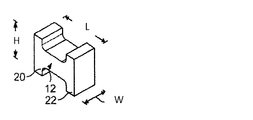
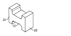
図3および図4は、電子構成部品10の別の実施形態の斜視図であり、H字形形態で(図3)、または犬の骨もしくはダンベル構成で(図4)示されている。図5に示されている実施形態では、図4のH字形チップフォームが使用される。これらの実施形態では、チップの高さ(H)、長さ(L)、および幅(W)が構成部品に関して示されている。図5A〜Dは、H字形チップフォームの一実施形態のそれぞれ斜視図、正面図、側面図、および底面図である。本明細書に記載のように、驚くべきことに、電子構成部品がある長さ対幅比を有するようにこれらの寸法を操作することにより、構成部品の性能に著しく負の影響を及ぼすことなしに、構成部品のサイズを縮小することができ、さらには性能パラメータが改善することを可能にすることが発見された。
3 and 4 are perspective views of another embodiment of the
本記載の改善された電子構成部品を開発する際、1GHzより大きいSRF値を生じた400〜600nHの範囲内のインダクタンス値を有し、一方、0.36mm未満の構成部品幅を有する、または他の方法で0402シリーズチップのボード面積サイズを少なくとも60%縮小するインダクタを提供するという目的があった。0402シリーズチップは、約0.52mm2のボード面積を示すので、この目的は、ボード面積が0.21mm2(0.52からの60%縮小を表す)より小さい構成部品を作り出すことであった。 When developing the improved electronic component of this description, it has an inductance value in the range of 400-600 nH that produced an SRF value greater than 1 GHz, while having a component width of less than 0.36 mm, or others In this way, an inductor is provided which reduces the board area size of the 0402 series chip by at least 60%. 0402 series chip exhibits a board area of about 0.52 mm 2, this object is achieved, board area (representing 60% reduction from 0.52) 0.21 mm 2 was to create a smaller component .

表1は、これらの目的を念頭にテストされた様々な電子構成部品の性能値を示す。より具体的には、表1は、互いに照らしてテストされた560nHのインダクタンスを有する6つの異なる電子構成部品の様々なパラメータおよび値を示す。表1において0402および0201として識別されている最初の2つの構成部品は、従来技術の構成部品を表す。0402構成部品は、本明細書で論じられている従来技術の0402シリーズチップを表し、これに照らしてサイズ縮小が測定される。名前が示すように、0402構成部品は、40ミル(または0.040インチ(1.02mm))の長さ、および20ミル(または0.020インチ(0.508mm))の幅を有し、それにより2.0の長さ対幅比をもたらす。表でわかるように、この製品は、1.0GHz閾値より大きい1.2GHzのSRFを有するが、0.52mm2のボード面積を有する。第2の従来技術の構成部品、0201デバイスは、1.70対1の長さ対幅比を有する。この構成部品は、ボード面積サイズを0.144mm2に著しく縮小したが、1.0GHzSRF値の目標を達成することができなかった。 Table 1 shows the performance values of various electronic components tested with these objectives in mind. More specifically, Table 1 shows various parameters and values for six different electronic components having an inductance of 560 nH tested against each other. The first two components identified as 0402 and 0201 in Table 1 represent prior art components. The 0402 component represents the prior art 0402 series chip discussed herein, and the size reduction is measured in light of this. As the name implies, the 0402 component has a length of 40 mils (or 0.040 inches (1.02 mm)) and a width of 20 mils (or 0.020 inches (0.508 mm)); This results in a length to width ratio of 2.0. As can be seen in the table, this product has a 1.2 GHz SRF greater than the 1.0 GHz threshold, but has a board area of 0.52 mm 2 . The second prior art component, the 0201 device, has a length to width ratio of 1.70 to 1. This component significantly reduced the board area size to 0.144 mm 2 but failed to achieve the 1.0 GHz SRF value target.
この範囲(spectrum)の他端では、テストサンプル4は、3.25の長さ対幅比を有する構成部品であった。この構成部品は、1.0GHzSRF値を満たすことができるが、ボード面積は、0.25mm2に縮小されただけであり、これは、0402シリーズチップから50%を超えるサイズ減を依然として表しているが、60%サイズ減の目的を満たすには十分でなかった。 At the other end of the spectrum, test sample 4 was a component having a length to width ratio of 3.25. This component can meet the 1.0 GHz SRF value, but the board area has only been reduced to 0.25 mm 2 , which still represents over 50% size reduction from the 0402 series chip. However, it was not enough to meet the purpose of 60% size reduction.
400〜600nH範囲内のインダクタンス値について1GHzSRFのこれらの目的を満たすためには、驚くべきことに、構成部品の長さ対幅比を約2.1から約2.5の範囲内に修正することにより、これらの結果を達成することができることが発見された。表1が示すように、サンプル1、2、3はそれぞれ、60%を超えるサイズ減を示し、一方、1.0GHzの最小SRFの目的を満たすこともできる電子構成部品を表す。これらの構成部品のそれぞれは、約2.1から約2.4の範囲内の長さ対幅比で作り出される。これらの3つのサンプルのうち、サンプル1は、0.17mm2のボード面積および1.7GHzの最高SRF値を有する最も小さい構成部品をもたらしたが、150nH/Ω(高いことが望ましい特性)のインダクタンス対DCR比は、サンプル2、3のものより低かった。サンプル2は、サンプル1のものより著しく高い240nH/Ωのインダクタンス対DCR比を有する、サイズおよびSRF値がサンプル1のものに非常に似ている構成部品(それぞれ0.18mm2および1.6GHz)を表す。したがって、いくつかの例では、約2.2から2.4の範囲内、より具体的には2.4の長さ対幅比を有する電子構成部品が、構成部品のサイズおよび性能特性を最適化することになる。 In order to meet these objectives of 1 GHz SRF for inductance values in the 400-600 nH range, surprisingly the component length to width ratio is modified within the range of about 2.1 to about 2.5. It was discovered that these results can be achieved. As Table 1 shows, Samples 1, 2, and 3 each represent an electronic component that exhibits a size reduction greater than 60%, while also meeting the objective of a minimum SRF of 1.0 GHz. Each of these components is produced with a length to width ratio in the range of about 2.1 to about 2.4. Of these three samples, sample 1 resulted in the smallest component with a board area of 0.17 mm 2 and a maximum SRF value of 1.7 GHz, but with an inductance of 150 nH / Ω (a characteristic that is desired to be high) The ratio to DCR was lower than that of samples 2 and 3. Sample 2 has a 240 nH / Ω inductance to DCR ratio that is significantly higher than that of Sample 1 and is very similar in size and SRF value to those of Sample 1 (0.18 mm 2 and 1.6 GHz, respectively) Represents. Thus, in some instances, an electronic component having a length to width ratio in the range of about 2.2 to 2.4, and more specifically 2.4, optimizes component size and performance characteristics. It will become.
本開示は、表面実装誘導性構成部品の例を提供する。構成部品は、主水平部分と、そこから延びるサポートとを有する小型チップフォームを含む。いくつかの例はパッドをも含み、たとえばチップフォームをプリント回路板に電気的に接続するためにサポートに接続された金属化パッドを含む。ワイヤが、チップフォームの主水平部分の少なくとも一部分の周りに巻かれる。ワイヤは、たとえば52ゲージから56ゲージのワイヤ(たとえば、54ゲージのワイヤ)とすることができる。ワイヤは、第1の端部および第2の端部がそれぞれのパッドに接続されている。誘導性構成部品は、約2.1から約2.5の範囲内の長さ対幅比を有する。いくつかの例では、誘導性構成部品は、約2.2から約2.4の範囲内の長さ対幅比を有する。他の例では、誘導性構成部品は、約2.4の長さ対幅比を有する。 The present disclosure provides examples of surface mount inductive components. The component includes a small chip form having a main horizontal portion and a support extending therefrom. Some examples also include pads, such as metallized pads connected to a support to electrically connect the chip form to a printed circuit board. A wire is wound around at least a portion of the main horizontal portion of the chip foam. The wire can be, for example, a 52 gauge to 56 gauge wire (eg, a 54 gauge wire). The wire has a first end and a second end connected to the respective pads. The inductive component has a length to width ratio in the range of about 2.1 to about 2.5. In some examples, the inductive component has a length to width ratio in the range of about 2.2 to about 2.4. In another example, the inductive component has a length to width ratio of about 2.4.
いくつかの実施形態では、誘導性構成部品は、コアを含む。誘導性構成部品および/またはコアは、フェライト材料を含むことができる。また、誘導性構成部品および/またはコアは、犬の骨、ダンベル、またはH字形構成の少なくとも1つを含むことができる。 In some embodiments, the inductive component includes a core. The inductive component and / or the core can include a ferrite material. The inductive component and / or core can also include at least one of a dog bone, a dumbbell, or an H-shaped configuration.
いくつかの実施形態は、約400nHから約600nHの範囲内のインダクタンス、より具体的には、約560nHのインダクタンスを有する誘導性構成部品を含む。 Some embodiments include inductive components having an inductance in the range of about 400 nH to about 600 nH, and more specifically, an inductance of about 560 nH.
誘導性構成部品は、1GHzより大きいSRFを示す。いくつかの例では、構成部品は、少なくとも約1.2GHz、少なくとも約1.5GHz、少なくとも約1.6GHz、または少なくとも約1.7GHzのSRFを示す。 Inductive components exhibit an SRF greater than 1 GHz. In some examples, the component exhibits an SRF of at least about 1.2 GHz, at least about 1.5 GHz, at least about 1.6 GHz, or at least about 1.7 GHz.
いくつかの例では、誘導性構成部品は、約550nH/Ω以下のインダクタンス対DCR比を示す。他の例では、誘導性構成部品は、約510nH/Ω、約300nH/Ω、約240nH/Ω、または約150nH/Ω以下のインダクタンス対DCR比を示す。 In some examples, the inductive component exhibits an inductance to DCR ratio of about 550 nH / Ω or less. In other examples, the inductive component exhibits an inductance to DCR ratio of about 510 nH / Ω, about 300 nH / Ω, about 240 nH / Ω, or about 150 nH / Ω or less.
誘導性構成部品は、約0.36mm未満の幅を有する。誘導性構成部品のいくつかの例は、約0.25mm2以下のボード面積を有することになる。いくつかの例では、誘導性構成部品は、誘導性構成部品は、0.21mm2以下、または約0.52mm2の面積を有する0402シリーズチップのものより60%小さい面積を有することになる。他の例では、誘導性構成部品は、約0.20mm2以下、約0.18mm2以下、または約0.17mm2以下のボード面積を有することになる。 The inductive component has a width of less than about 0.36 mm. Some examples of inductive components will have a board area of about 0.25 mm 2 or less. In some examples, inducible components, inductive components, will have a 60% smaller area than that of the 0402 series chip having an area of 0.21 mm 2 or less, or about 0.52 mm 2. In other examples, inducible component is about 0.20 mm 2 or less, will have about 0.18 mm 2 or less, or about 0.17 mm 2 or less board space.
いくつかの形態では、誘導性構成部品は、約2.4対1の長さ対幅比、約0.18mm2のボード面積、約1.6GHzのSRF値、約240nH/Ωのインダクタンス対DCR比、および/または約2.4:1GHz/mmのSRF/長さ比を有する。 In some forms, the inductive component has a length to width ratio of about 2.4 to 1, a board area of about 0.18 mm 2 , an SRF value of about 1.6 GHz, and an inductance to DCR of about 240 nH / Ω. Ratio, and / or SRF / length ratio of about 2.4: 1 GHz / mm.
電子構成部品は、52ゲージから56ゲージの範囲内のワイヤを使用することができる。たとえば、電子構成部品は、54ゲージのワイヤを使用することができる。 Electronic components can use wires in the 52 gauge to 56 gauge range. For example, an electronic component can use a 54 gauge wire.
電子構成部品は、硬磁性材料および軟磁性材料、ならびに/またはフェライトなど、磁性材料を含めて、様々な材料から形成され、またはそれらを含むことができる。 The electronic components can be formed from or include various materials, including magnetic materials such as hard and soft magnetic materials, and / or ferrite.
本記載の電子構成部品は、たとえば、スマートフォンまたは手首着用のモバイル電子デバイス(たとえば、スマートウォッチ)などモバイル電子デバイスを含めて、様々なデバイスで使用され得る。 The electronic components described herein may be used in a variety of devices, including, for example, mobile electronic devices such as smartphones or wrist-worn mobile electronic devices (eg, smart watches).
本開示はまた、電子構成部品を形成する方法を提供する。一例では、この方法は、コアおよび/または電子構成部品、たとえば本明細書に記載のコアおよび/または構成部品のうちの1つを提供することを含む。いくつかの実施形態では、コア/構成部品は、ワイヤが巻かれ得る狭い部分(たとえば、縮小された直径/幅部分)を有する。コア/構成部品は、約2.1から約2.5の範囲内の長さ対幅比を有する。この方法は、狭い部分周りに第1の端部および第2の端部を有するワイヤ(たとえば、54ゲージのワイヤ、または52ゲージから56ゲージの範囲内の他のワイヤ)を含む。この方法は、第1の端部および第2の端部を端子に接続すること、または電子構成部品を回路に取り付けるために第1の端部および第2の端部から端子を形成することをさらに含む。 The present disclosure also provides a method of forming an electronic component. In one example, the method includes providing a core and / or electronic component, eg, one of the cores and / or components described herein. In some embodiments, the core / component has a narrow portion (eg, reduced diameter / width portion) around which the wire can be wound. The core / component has a length to width ratio in the range of about 2.1 to about 2.5. The method includes a wire having a first end and a second end around a narrow portion (eg, a 54 gauge wire or other wires in the 52 gauge to 56 gauge range). The method includes connecting a first end and a second end to a terminal, or forming a terminal from the first end and the second end for attaching an electronic component to a circuit. In addition.
ワイヤの第1のもの、および第2のものは、構成部品が従来のはんだ付け技法を介してPCBにはんだ付けされたとき構成部品とPCBとの間に強い電気接続がなされるように、端子を形成するために厚膜を金属化する際に埋め込まれ得る。しかし、代替的実施形態では、ワイヤ端部は、端子に積み重ねること、または溶接することによってなど、他の従来の方法を使用して、構成部品の端子または他のパッドに接続されてもよい。 The first and second of the wires are terminals so that a strong electrical connection is made between the component and the PCB when the component is soldered to the PCB via conventional soldering techniques. Can be embedded in metallizing the thick film to form However, in alternative embodiments, the wire ends may be connected to the terminals or other pads of the component using other conventional methods, such as by stacking or welding to the terminals.
本開示は、本技術の好ましい実施形態および例について述べている。当業者なら、特許請求の範囲に記載の本発明の範囲から逸脱することなしに上述の実施形態に関して多種多様な修正、変更、および組合せをなすことができること、およびそのような修正、変更、および組合せは、本発明の概念の範囲内にあると見なされるべきであることを理解するであろう。さらに、一実施形態の特徴は、望むならさらに他の実施形態を提供するように他の実施形態の特徴と組み合わされ得ることをも理解されたい。本開示内に引用されている参照はすべて、参照によりそれらの全体が本明細書に組み込まれる。 This disclosure describes preferred embodiments and examples of the present technology. Those skilled in the art can make various modifications, changes, and combinations with respect to the above-described embodiments without departing from the scope of the present invention as set forth in the claims, and such modifications, changes, and It will be understood that combinations should be considered within the scope of the inventive concept. Further, it should be understood that the features of one embodiment may be combined with the features of other embodiments to provide further embodiments if desired. All references cited within this disclosure are incorporated herein by reference in their entirety.
10 電子構成部品
12 コア
12a、32a 第1の端部
12b、32b 第2の端部
12c 主水平区間
20 第1のサポート
22 第2のサポート
28、30 金属化パッド
32 ワイヤ
38 カバー
DESCRIPTION OF
Claims (33)
主水平部分、およびそこから延びるサポートを有する小型チップフォームと、
前記チップフォームをプリント回路板に電気的に接続するために前記サポートに接続された端子と、
前記チップフォームの前記主水平部分の少なくとも一部分の周りに巻かれたワイヤであって、前記端子を形成する、またはそれぞれの端子に接続される第1の端部および第2の端部を有するワイヤとを備え、
約2.1から約2.5の範囲内の長さ対幅比を有することを特徴とする誘導性構成部品。 A surface mountable inductive component,
A small chip foam having a main horizontal portion and a support extending therefrom;
Terminals connected to the support for electrically connecting the chip form to a printed circuit board;
A wire wound around at least a portion of the main horizontal portion of the chipform, the wire forming a terminal or having a first end and a second end connected to each terminal And
An inductive component having a length to width ratio in the range of about 2.1 to about 2.5.
主水平部分、およびそこから延びる細長い端部を有する小型チップフォームであって、前記水平部分は、前記細長い端部より小さい断面を有する、小型チップフォームと、
前記チップフォームの前記主水平部分の少なくとも一部分の周りに巻かれたワイヤであって、構成部品を回路に取り付けるために各細長い端部に接続される、または各細長い端部上にそれぞれの端子を形成する第1の端部および第2の端部を有するワイヤとを備え、
約2.1から約2.5の範囲内の長さ対幅比を有することを特徴とする誘導性構成部品。 A surface mountable inductive component,
A small chip foam having a main horizontal portion and an elongated end extending therefrom, the horizontal portion having a smaller cross-section than the elongated end;
A wire wound around at least a portion of the main horizontal portion of the chip form, connected to each elongated end for attaching a component to a circuit, or a respective terminal on each elongated end A wire having a first end and a second end to be formed,
An inductive component having a length to width ratio in the range of about 2.1 to about 2.5.
Applications Claiming Priority (2)
| Application Number | Priority Date | Filing Date | Title |
|---|---|---|---|
| US201562248923P | 2015-10-30 | 2015-10-30 | |
| US62/248,923 | 2015-10-30 |
Publications (2)
| Publication Number | Publication Date |
|---|---|
| JP3204112U true JP3204112U (en) | 2016-05-12 |
| JP3204112U7 JP3204112U7 (en) | 2016-12-22 |
Family
ID=55952095
Family Applications (1)
| Application Number | Title | Priority Date | Filing Date |
|---|---|---|---|
| JP2016000862U Active JP3204112U (en) | 2015-10-30 | 2016-02-25 | Electronic components |
Country Status (4)
| Country | Link |
|---|---|
| US (1) | US20170125157A1 (en) |
| JP (1) | JP3204112U (en) |
| CN (1) | CN205656934U (en) |
| MY (1) | MY188109A (en) |
Cited By (5)
| Publication number | Priority date | Publication date | Assignee | Title |
|---|---|---|---|---|
| JP2018142644A (en) * | 2017-02-28 | 2018-09-13 | 株式会社村田製作所 | Inductor |
| CN108735425A (en) * | 2017-04-19 | 2018-11-02 | 株式会社村田制作所 | Inductor components |
| JP2018186159A (en) * | 2017-04-25 | 2018-11-22 | 株式会社村田製作所 | Inductor |
| JP2021012920A (en) * | 2019-07-04 | 2021-02-04 | 株式会社村田製作所 | Inductor component |
| US11972887B2 (en) | 2019-07-04 | 2024-04-30 | Murata Manufacturing Co., Ltd. | Inductor component |
Families Citing this family (5)
| Publication number | Priority date | Publication date | Assignee | Title |
|---|---|---|---|---|
| JP6791068B2 (en) * | 2017-08-29 | 2020-11-25 | 株式会社村田製作所 | Coil parts and mounting board with coil parts |
| JP6769450B2 (en) * | 2018-01-30 | 2020-10-14 | 株式会社村田製作所 | Inductor parts |
| JP7247779B2 (en) * | 2019-06-21 | 2023-03-29 | 株式会社村田製作所 | wire wound inductor components |
| JP2021002577A (en) * | 2019-06-21 | 2021-01-07 | 株式会社村田製作所 | Winding-type inductor component |
| CN113436831A (en) * | 2021-07-19 | 2021-09-24 | 惠州市德立电子有限公司 | Miniature inductor |
Citations (2)
| Publication number | Priority date | Publication date | Assignee | Title |
|---|---|---|---|---|
| JP2005057104A (en) * | 2003-08-06 | 2005-03-03 | Nec Tokin Corp | Choke coil and its manufacturing method |
| JP2015070016A (en) * | 2013-09-27 | 2015-04-13 | 株式会社村田製作所 | Coil component |
Family Cites Families (13)
| Publication number | Priority date | Publication date | Assignee | Title |
|---|---|---|---|---|
| TW342506B (en) * | 1996-10-11 | 1998-10-11 | Matsushita Electric Ind Co Ltd | Inductance device and wireless terminal equipment |
| US6437676B1 (en) * | 1999-06-29 | 2002-08-20 | Matsushita Electric Industrial Co., Ltd. | Inductance element |
| TW541556B (en) * | 2000-12-27 | 2003-07-11 | Matsushita Electric Ind Co Ltd | Circuit protector |
| JP4532167B2 (en) * | 2003-08-21 | 2010-08-25 | コーア株式会社 | Chip coil and substrate with chip coil mounted |
| WO2005056734A2 (en) * | 2003-12-03 | 2005-06-23 | Coilcraft, Incorporated | Electronic component |
| JP2005210055A (en) * | 2003-12-22 | 2005-08-04 | Taiyo Yuden Co Ltd | Surface mount coil part and manufacturing method of the same |
| JP4780111B2 (en) * | 2005-11-22 | 2011-09-28 | 株式会社村田製作所 | Winding type coil |
| WO2007080680A1 (en) * | 2006-01-16 | 2007-07-19 | Murata Manufacturing Co., Ltd. | Method for manufacturing inductor |
| EP2087494B1 (en) * | 2006-12-01 | 2016-11-23 | Murata Manufacturing Co. Ltd. | Common mode choke coil |
| KR101872529B1 (en) * | 2012-06-14 | 2018-08-02 | 삼성전기주식회사 | Multi-layered chip electronic component |
| KR101771731B1 (en) * | 2012-08-28 | 2017-08-25 | 삼성전기주식회사 | Multi-layered chip electronic component |
| KR102120898B1 (en) * | 2014-06-19 | 2020-06-09 | 삼성전기주식회사 | Chip coil component |
| KR101580411B1 (en) * | 2014-09-22 | 2015-12-23 | 삼성전기주식회사 | Chip electronic component and board having the same mounted thereon |
-
2016
- 2016-02-24 CN CN201620139625.0U patent/CN205656934U/en active Active
- 2016-02-25 JP JP2016000862U patent/JP3204112U/en active Active
- 2016-08-17 MY MYPI2016702991A patent/MY188109A/en unknown
- 2016-10-28 US US15/337,282 patent/US20170125157A1/en not_active Abandoned
Patent Citations (2)
| Publication number | Priority date | Publication date | Assignee | Title |
|---|---|---|---|---|
| JP2005057104A (en) * | 2003-08-06 | 2005-03-03 | Nec Tokin Corp | Choke coil and its manufacturing method |
| JP2015070016A (en) * | 2013-09-27 | 2015-04-13 | 株式会社村田製作所 | Coil component |
Cited By (11)
| Publication number | Priority date | Publication date | Assignee | Title |
|---|---|---|---|---|
| JP2018142644A (en) * | 2017-02-28 | 2018-09-13 | 株式会社村田製作所 | Inductor |
| US10867738B2 (en) | 2017-02-28 | 2020-12-15 | Murata Manufacturing Co., Ltd. | Inductor |
| CN108735425A (en) * | 2017-04-19 | 2018-11-02 | 株式会社村田制作所 | Inductor components |
| JP2018182182A (en) * | 2017-04-19 | 2018-11-15 | 株式会社村田製作所 | Inductor |
| CN108735425B (en) * | 2017-04-19 | 2020-12-01 | 株式会社村田制作所 | Inductor component |
| US11170929B2 (en) | 2017-04-19 | 2021-11-09 | Murata Manufacturing Co., Ltd. | Inductor component |
| JP2018186159A (en) * | 2017-04-25 | 2018-11-22 | 株式会社村田製作所 | Inductor |
| US11127526B2 (en) | 2017-04-25 | 2021-09-21 | Murata Manufacturing Co., Ltd. | Inductor component |
| JP2021012920A (en) * | 2019-07-04 | 2021-02-04 | 株式会社村田製作所 | Inductor component |
| JP7147699B2 (en) | 2019-07-04 | 2022-10-05 | 株式会社村田製作所 | inductor components |
| US11972887B2 (en) | 2019-07-04 | 2024-04-30 | Murata Manufacturing Co., Ltd. | Inductor component |
Also Published As
| Publication number | Publication date |
|---|---|
| CN205656934U (en) | 2016-10-19 |
| US20170125157A1 (en) | 2017-05-04 |
| MY188109A (en) | 2021-11-20 |
Similar Documents
| Publication | Publication Date | Title |
|---|---|---|
| JP3204112U (en) | Electronic components | |
| US8339233B2 (en) | Three dimensional inductor | |
| US10867738B2 (en) | Inductor | |
| CN106373709B (en) | Module substrate | |
| US10878993B2 (en) | Inductor | |
| JP6669123B2 (en) | Inductor | |
| JP6708162B2 (en) | Inductor | |
| EP1763044B1 (en) | Inductor | |
| US20050145408A1 (en) | Electronic component | |
| JP6720914B2 (en) | Inductor | |
| JP2015144166A (en) | Electronic component | |
| JP2008103430A (en) | Inductor | |
| CN108987040B (en) | Inductor | |
| JP2018186159A (en) | Inductor | |
| JP2001185422A (en) | Induction parts having low height outer shape | |
| KR20160032566A (en) | Coil component and and board for mounting the same | |
| JP6769450B2 (en) | Inductor parts | |
| CN211507262U (en) | Wound inductor component | |
| KR20180071827A (en) | Magnetic core, inductor and emi filter comprising the same | |
| US20190214184A1 (en) | Inductor with coil conductor formed by conductive material | |
| KR20180071828A (en) | Magnetic core, inductor and emi filter comprising the same | |
| KR20180017409A (en) | Inductor | |
| JP2004006696A (en) | Wire-wound inductor | |
| CN213905093U (en) | Inductor core assembly and inductor including the same | |
| JP2000306749A (en) | Choke coil |
Legal Events
| Date | Code | Title | Description |
|---|---|---|---|
| R150 | Certificate of patent or registration of utility model |
Ref document number: 3204112 Country of ref document: JP Free format text: JAPANESE INTERMEDIATE CODE: R150 |
|
| A623 | Registrability report |
Free format text: JAPANESE INTERMEDIATE CODE: A623 Effective date: 20160629 |
|
| A623 | Registrability report |
Free format text: JAPANESE INTERMEDIATE CODE: A623 Effective date: 20160926 |
|
| R231 | Written correction (descriptions, etc.) |
Free format text: JAPANESE INTERMEDIATE CODE: R231 |
|
| R157 | Certificate of patent or utility model (correction) |
Free format text: JAPANESE INTERMEDIATE CODE: R157 |
|
| R250 | Receipt of annual fees |
Free format text: JAPANESE INTERMEDIATE CODE: R250 |
|
| R250 | Receipt of annual fees |
Free format text: JAPANESE INTERMEDIATE CODE: R250 |
|
| R250 | Receipt of annual fees |
Free format text: JAPANESE INTERMEDIATE CODE: R250 |
|
| R250 | Receipt of annual fees |
Free format text: JAPANESE INTERMEDIATE CODE: R250 |
|
| R250 | Receipt of annual fees |
Free format text: JAPANESE INTERMEDIATE CODE: R250 |