JP3142494U - Dark field illumination detector - Google Patents
Dark field illumination detector Download PDFInfo
- Publication number
- JP3142494U JP3142494U JP2008002098U JP2008002098U JP3142494U JP 3142494 U JP3142494 U JP 3142494U JP 2008002098 U JP2008002098 U JP 2008002098U JP 2008002098 U JP2008002098 U JP 2008002098U JP 3142494 U JP3142494 U JP 3142494U
- Authority
- JP
- Japan
- Prior art keywords
- light
- field illumination
- cavity
- dark field
- illumination detection
- Prior art date
- Legal status (The legal status is an assumption and is not a legal conclusion. Google has not performed a legal analysis and makes no representation as to the accuracy of the status listed.)
- Expired - Fee Related
Links
Images


Abstract
【課題】光源の照射角度の調節により、表面欠陥の検出が容易な暗視野照明検出装置を提供する。
【解決手段】内部表面が吸光面11であり、上部に開口部12が設けられていてるキャビティ1と、キャビティ1の吸光面11に環状に配置されている帯体2と、帯体2上に配置され、互いに電気的に接続されている複数の発光デバイス3と、キャビティ1の開口部12に対応する位置に配置され、キャビティ1内部で反射または屈折された光線を集光し、結像する板体4とを備える。
【選択図】図2Disclosed is a dark field illumination detection device that can easily detect a surface defect by adjusting an irradiation angle of a light source.
A cavity 1 whose inner surface is a light-absorbing surface 11, an opening 12 is provided at an upper portion thereof, a band 2 disposed in an annular shape on the light-absorbing surface 11 of the cavity 1, and a band 2 A plurality of light emitting devices 3 that are arranged and electrically connected to each other and a position that corresponds to the opening 12 of the cavity 1, and collects and forms an image of the light reflected or refracted inside the cavity 1. A plate 4 is provided.
[Selection] Figure 2
Description
本考案は、光学装置に関し、特に、表面欠陥を検出する暗視野照明検出装置に関する。 The present invention relates to an optical device, and more particularly to a dark field illumination detection device for detecting surface defects.
暗視野照明技術は、鏡面構造を有するデバイスまたは物体の検査に幅広く用いられている。例えば、宝石や半導体デバイスの表面欠陥の検出に用いられている。暗視野照明技術は、光源を配置し、この光源から照射される光線を直接検査対象物体に照射する。検出対象物体が有する光線の拡散反射または屈折の特性により、照射光線を反射または屈折させ結像する。この像により、表面に欠陥がないかどうか検査する。 Dark field illumination technology is widely used for inspection of devices or objects having a specular structure. For example, it is used for detecting surface defects of jewelry and semiconductor devices. In the dark field illumination technique, a light source is arranged, and a light beam emitted from the light source is directly irradiated onto an object to be inspected. An image is formed by reflecting or refracting the irradiated light beam based on the diffuse reflection or refraction property of the light beam of the detection target object. This image is inspected for defects on the surface.
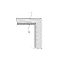
以下、図面に基づいて従来技術を説明する。図1は、従来技術による暗視野照明検出装置を示す断面図である。図1に示すように、従来技術による暗視野照明検出装置は、内部表面が吸光面であるキャビティ10を含む。キャビティ10の頂端には開口部101が設けられて、開口部101に対応する位置に板体20が配置されている。キャビティ10内の底部には発光デバイス30が配置され、発光デバイス30の周囲には複数の導光管40が配置されている。導光管40は、発光デバイス30の位置から光線を検査対象物体50まで導光する。検査対象物体50は、遮光板102上に配置され、遮光板102により発光デバイス30が照射する光線が遮断され、導光管40に導光された光線により検査対象物体50が直接照射される。検査対象物体50が有する光線の拡散反射または屈折の特性により、光線が板体20に集光され、結像する。この像により、表面に欠陥がないかどうか判断される。
The prior art will be described below with reference to the drawings. FIG. 1 is a cross-sectional view illustrating a conventional dark field illumination detection apparatus. As shown in FIG. 1, the dark field illumination detection apparatus according to the prior art includes a
従来技術による暗視野照明検出装置は、導光管40を導光経路として利用し、暗視野照明検出装置の光源を提供していた。検査対象物体50は、遮光板102上に直接配置されるため、異なる位置の表面欠陥を検査する場合、わざわざ位置を変える必要があり、検査効率に影響を与えていた。また、導光管40を導光経路として間接的に照射する方法は、光線不足のため、光線の拡散反射または屈折により十分に結像できないことも多く、判別時における精度の低さが検査結果に影響を与えてしまった。そのため、上記の問題点を改善する方法が求められていた。
本考案の目的は、光源の照射角度の調節により、表面欠陥の検出が容易な暗視野照明検出装置を提供することにある。 An object of the present invention is to provide a dark field illumination detection device that can easily detect surface defects by adjusting the irradiation angle of a light source.
上述の目的を達成するため、本考案は、暗視野照明検出装置を提供する。本考案の暗視野照明検出装置は、内部表面が吸光面であり、上部に開口部が設けられていてるキャビティと、キャビティの吸光面に環状に配置されている帯体と、帯体上に配置され、互いに電気的に接続されている複数の発光デバイスと、キャビティの開口部に対応する位置に配置され、キャビティ内部で反射または屈折された光線を集光し、結像する板体とを備える。検査対象物体に照射された光線が反射または屈折されて、キャビティの開口部上の板体に集光され、結像する。この像により、表面に欠陥がないかどうか判断される。 In order to achieve the above object, the present invention provides a dark field illumination detection apparatus. The dark field illumination detection device of the present invention has a cavity whose inner surface is a light absorption surface, an opening is provided in the upper part, a band disposed in a ring shape on the light absorption surface of the cavity, and a band disposed on the band A plurality of light-emitting devices electrically connected to each other, and a plate that is disposed at a position corresponding to the opening of the cavity, collects the light reflected or refracted inside the cavity, and forms an image. . The light beam applied to the object to be inspected is reflected or refracted and collected on a plate on the opening of the cavity to form an image. From this image, it is determined whether the surface is free from defects.
本考案の暗視野照明検出装置は、光源の照射角度の調節が可能になり、検査対象物体の位置をわざわざ変える必要がなくなり、検査効率を向上させることができる。また、光源の照射する光線の量が十分なため、十分に結像でき、精度の高い検査結果を得ることができる。 The dark field illumination detection device of the present invention can adjust the irradiation angle of the light source, and it is not necessary to change the position of the object to be inspected, thereby improving the inspection efficiency. Further, since the amount of light emitted from the light source is sufficient, it is possible to form an image sufficiently and obtain a highly accurate inspection result.
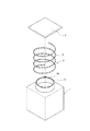
以下、本考案の実施形態を図面に基づいて説明する。図2は、本考案の一実施形態による暗視野照明検出装置を示す斜視図である。図3は、本考案の一実施形態による暗視野照明検出装置を示す断面図である。図5は、本考案のもう1つの実施形態による吸光面を示す断面図である。図2、図3および図5に示すように、本考案の一実施形態による暗視野照明検出装置は、内部表面が吸光面11であるキャビティ1を含む。吸光面11は、黒色材料からなり、本実施形態における材料は、黒色顔料である。吸光面11は、図5に示すように、黒色の布からなってもよい。キャビティ1は、上部に開口部12が設けられていて、内部の吸光面11には、帯体2が環状に配置されている。帯体2には、複数の発光デバイス3が配置され、本実施形態における発光デバイス3は、発光ダイオードであり、帯体2上の発光ダイオードは、互いに電気的に接続されている。キャビティ1の開口部12の上方の位置には、板体4が配置されている。板体4は、キャビティ1内で照射される光線を遮断し、同時に、キャビティ1内部で反射した光線を板体4上で結像する。
Embodiments of the present invention will be described below with reference to the drawings. FIG. 2 is a perspective view illustrating a dark field illumination detection apparatus according to an embodiment of the present invention. FIG. 3 is a cross-sectional view illustrating a dark field illumination detection apparatus according to an embodiment of the present invention. FIG. 5 is a cross-sectional view illustrating a light absorption surface according to another embodiment of the present invention. As shown in FIGS. 2, 3, and 5, the dark-field illumination detection device according to an embodiment of the present invention includes a
図3を参照する。本考案の暗視野照明検出装置は、鏡面または曲面を有する検査対象物体5を検査するのに用いられる。例えば、宝石や鏡面を有する半導体デバイスのように、検査対象物体5は、光線の拡散反射または屈折の特性を有する。検査対象物体5は、キャビティ1の内部にぶら下げられている。検査対象物体5の周辺の帯体2には、電力が供給され、帯体2上の複数の発光デバイス3が照射する光線が検査対象物体5の表面を直接照射する。検査対象物体5が有する光線の拡散反射または屈折の特性により、検査対象物体5に照射された光線が反射または屈折されて、キャビティ1内の吸光面11に吸収される光線以外の反射または屈折された光線(矢印で示す)は、キャビティ1の開口部12上の板体4に集光され、結像する。この像により、表面に欠陥がないかどうか判断される。
Please refer to FIG. The dark field illumination detection apparatus of the present invention is used for inspecting an
図4は、考案のもう1つの実施形態による暗視野照明検出装置を示す斜視図である。図4に示すように、本考案のもう1つの実施形態による暗視野照明検出装置は、帯体2の形状において、上記の1つの帯体2がキャビティ1の吸光面11上に環状に配置される以外に、環状帯体2にすることもできる。キャビティ1内の吸光面11上に間隔を空けて環状帯体2が配置され、同一の帯体2上の複数の発光デバイス3は、互いに電気的に接続されている。異なる帯体2の上の発光デバイス3の発光を制御することにより、異なる角度の光線を検査対象物体5に照射し、異なる表面に欠陥がないかどうか判断される。
FIG. 4 is a perspective view illustrating a dark field illumination detection apparatus according to another embodiment of the invention. As shown in FIG. 4, in the dark field illumination detection apparatus according to another embodiment of the present invention, in the shape of the
本考案では好適な実施形態を前述の通りに開示したが、これらは決して本考案を限定するものではなく、当該技術を熟知する者は誰でも、本考案の精神と領域を脱しない範囲内で各種の変更や修正を加えることができる。従って、本考案の保護の範囲は、実用新案請求の範囲で指定した内容を基準とする。 Although the present invention discloses preferred embodiments as described above, these are not intended to limit the present invention in any way, and anyone skilled in the art is within the spirit and scope of the present invention. Various changes and modifications can be made. Therefore, the scope of protection of the present invention is based on the contents specified in the claims of the utility model.
1 キャビティ
2 帯体
3 発光デバイス
4 板体
5 検査対象物体
11 吸光面
12 開口部
DESCRIPTION OF
Claims (7)
前記キャビティの前記吸光面に環状に配置されている帯体と、
前記帯体上に配置され、互いに電気的に接続されている複数の発光デバイスと、
前記キャビティの前記開口部に対応する位置に配置され、前記キャビティ内部で反射または屈折された光線を集光し、結像する板体とを備えることを特徴とする暗視野照明検出装置。 A cavity whose inner surface is a light-absorbing surface and has an opening at the top;
A band disposed annularly on the light-absorbing surface of the cavity;
A plurality of light emitting devices disposed on the strip and electrically connected to each other;
A dark-field illumination detection apparatus comprising: a plate that is disposed at a position corresponding to the opening of the cavity and collects and focuses a light beam reflected or refracted inside the cavity.
Applications Claiming Priority (1)
| Application Number | Priority Date | Filing Date | Title |
|---|---|---|---|
| TW96210809U TWM324200U (en) | 2007-07-03 | 2007-07-03 | Darkness lighting detector |
Publications (1)
| Publication Number | Publication Date |
|---|---|
| JP3142494U true JP3142494U (en) | 2008-06-12 |
Family
ID=39461704
Family Applications (1)
| Application Number | Title | Priority Date | Filing Date |
|---|---|---|---|
| JP2008002098U Expired - Fee Related JP3142494U (en) | 2007-07-03 | 2008-04-04 | Dark field illumination detector |
Country Status (2)
| Country | Link |
|---|---|
| JP (1) | JP3142494U (en) |
| TW (1) | TWM324200U (en) |
Families Citing this family (1)
| Publication number | Priority date | Publication date | Assignee | Title |
|---|---|---|---|---|
| CN102834704B (en) * | 2011-02-23 | 2015-11-25 | 联达科技检测私人有限公司 | The inspection of the defect in contact lenses |
-
2007
- 2007-07-03 TW TW96210809U patent/TWM324200U/en not_active IP Right Cessation
-
2008
- 2008-04-04 JP JP2008002098U patent/JP3142494U/en not_active Expired - Fee Related
Also Published As
| Publication number | Publication date |
|---|---|
| TWM324200U (en) | 2007-12-21 |
Similar Documents
| Publication | Publication Date | Title |
|---|---|---|
| JP4457100B2 (en) | Lighting device | |
| US9494422B2 (en) | Lighting device for inspection and lighting method for inspection | |
| US20080062424A1 (en) | Compact Ringlight | |
| TWI485387B (en) | Inspection apparatus for light emitting diode | |
| WO2007017941A1 (en) | Device for inspecting flaw at end section | |
| JP5740595B2 (en) | Outline detection method and outline detection apparatus | |
| KR101001113B1 (en) | Apparatus for Detecting Wafer Crack and Method for Detecting Wafer Defect | |
| JP3142494U (en) | Dark field illumination detector | |
| JP2017207380A (en) | Surface defect inspection device | |
| US8110804B2 (en) | Through substrate optical imaging device and method | |
| JP2006242814A (en) | Surface inspection device | |
| JP3360429B2 (en) | Lighting equipment for visual inspection | |
| JP2008096187A (en) | Edge-part flaw inspecting device | |
| JP6381865B2 (en) | Inspection apparatus and inspection method | |
| US7701569B2 (en) | Dark field lighting testing device | |
| JP4588361B2 (en) | External surface inspection device | |
| JP2008139126A (en) | Flaw detector and flaw detection method | |
| CN112782175A (en) | Detection equipment and detection method | |
| CN102313751B (en) | Chip LED detection device | |
| TWI479131B (en) | Testing apparatus for light emitting diodes | |
| JP7406984B2 (en) | UV irradiation device | |
| JP4117789B2 (en) | Surface light source device for surface inspection | |
| JP6864709B2 (en) | Seal appearance inspection method | |
| JP2008216149A (en) | Surface inspection device and method | |
| JP2007121120A (en) | Wafer visual inspection device |
Legal Events
| Date | Code | Title | Description |
|---|---|---|---|
| R150 | Certificate of patent or registration of utility model |
Free format text: JAPANESE INTERMEDIATE CODE: R150 |
|
| FPAY | Renewal fee payment (event date is renewal date of database) |
Free format text: PAYMENT UNTIL: 20110521 Year of fee payment: 3 |
|
| FPAY | Renewal fee payment (event date is renewal date of database) |
Free format text: PAYMENT UNTIL: 20110521 Year of fee payment: 3 |
|
| FPAY | Renewal fee payment (event date is renewal date of database) |
Free format text: PAYMENT UNTIL: 20120521 Year of fee payment: 4 |
|
| FPAY | Renewal fee payment (event date is renewal date of database) |
Free format text: PAYMENT UNTIL: 20120521 Year of fee payment: 4 |
|
| FPAY | Renewal fee payment (event date is renewal date of database) |
Free format text: PAYMENT UNTIL: 20130521 Year of fee payment: 5 |
|
| FPAY | Renewal fee payment (event date is renewal date of database) |
Free format text: PAYMENT UNTIL: 20140521 Year of fee payment: 6 |
|
| LAPS | Cancellation because of no payment of annual fees |