JP2025041295A - Acoustic wave device, filter, multiplexer, and method for manufacturing an acoustic wave device - Google Patents

Acoustic wave device, filter, multiplexer, and method for manufacturing an acoustic wave device Download PDF

Info

Publication number
JP2025041295A
JP2025041295A JP2023148488A JP2023148488A JP2025041295A JP 2025041295 A JP2025041295 A JP 2025041295A JP 2023148488 A JP2023148488 A JP 2023148488A JP 2023148488 A JP2023148488 A JP 2023148488A JP 2025041295 A JP2025041295 A JP 2025041295A
Authority
JP
Japan
Prior art keywords
film
piezoelectric layer
lower electrode
upper electrode
wave device
Prior art date
Legal status (The legal status is an assumption and is not a legal conclusion. Google has not performed a legal analysis and makes no representation as to the accuracy of the status listed.)
Pending
Application number
JP2023148488A
Other languages
Japanese (ja)
Inventor
倫仁 藤田
Norihito Fujita
Current Assignee (The listed assignees may be inaccurate. Google has not performed a legal analysis and makes no representation or warranty as to the accuracy of the list.)
Taiyo Yuden Co Ltd
Original Assignee
Taiyo Yuden Co Ltd
Priority date (The priority date is an assumption and is not a legal conclusion. Google has not performed a legal analysis and makes no representation as to the accuracy of the date listed.)
Filing date
Publication date
Application filed by Taiyo Yuden Co Ltd filed Critical Taiyo Yuden Co Ltd
Priority to JP2023148488A priority Critical patent/JP2025041295A/en
Priority to US18/824,825 priority patent/US20250088165A1/en
Priority to CN202411263508.0A priority patent/CN119628592A/en
Publication of JP2025041295A publication Critical patent/JP2025041295A/en
Pending legal-status Critical Current

Links

Images

Classifications

    • HELECTRICITY
    • H03ELECTRONIC CIRCUITRY
    • H03HIMPEDANCE NETWORKS, e.g. RESONANT CIRCUITS; RESONATORS
    • H03H9/00Networks comprising electromechanical or electro-acoustic elements; Electromechanical resonators
    • H03H9/15Constructional features of resonators consisting of piezoelectric or electrostrictive material
    • H03H9/17Constructional features of resonators consisting of piezoelectric or electrostrictive material having a single resonator
    • H03H9/171Constructional features of resonators consisting of piezoelectric or electrostrictive material having a single resonator implemented with thin-film techniques, i.e. of the film bulk acoustic resonator [FBAR] type
    • HELECTRICITY
    • H03ELECTRONIC CIRCUITRY
    • H03HIMPEDANCE NETWORKS, e.g. RESONANT CIRCUITS; RESONATORS
    • H03H3/00Apparatus or processes specially adapted for the manufacture of impedance networks, resonating circuits, resonators
    • H03H3/007Apparatus or processes specially adapted for the manufacture of impedance networks, resonating circuits, resonators for the manufacture of electromechanical resonators or networks
    • H03H3/02Apparatus or processes specially adapted for the manufacture of impedance networks, resonating circuits, resonators for the manufacture of electromechanical resonators or networks for the manufacture of piezoelectric or electrostrictive resonators or networks
    • HELECTRICITY
    • H03ELECTRONIC CIRCUITRY
    • H03HIMPEDANCE NETWORKS, e.g. RESONANT CIRCUITS; RESONATORS
    • H03H9/00Networks comprising electromechanical or electro-acoustic elements; Electromechanical resonators
    • H03H9/02Details
    • H03H9/02007Details of bulk acoustic wave devices
    • H03H9/02015Characteristics of piezoelectric layers, e.g. cutting angles
    • HELECTRICITY
    • H03ELECTRONIC CIRCUITRY
    • H03HIMPEDANCE NETWORKS, e.g. RESONANT CIRCUITS; RESONATORS
    • H03H9/00Networks comprising electromechanical or electro-acoustic elements; Electromechanical resonators
    • H03H9/02Details
    • H03H9/02007Details of bulk acoustic wave devices
    • H03H9/02086Means for compensation or elimination of undesirable effects
    • H03H9/02094Means for compensation or elimination of undesirable effects of adherence
    • HELECTRICITY
    • H03ELECTRONIC CIRCUITRY
    • H03HIMPEDANCE NETWORKS, e.g. RESONANT CIRCUITS; RESONATORS
    • H03H9/00Networks comprising electromechanical or electro-acoustic elements; Electromechanical resonators
    • H03H9/02Details
    • H03H9/125Driving means, e.g. electrodes, coils
    • H03H9/13Driving means, e.g. electrodes, coils for networks consisting of piezoelectric or electrostrictive materials
    • H03H9/131Driving means, e.g. electrodes, coils for networks consisting of piezoelectric or electrostrictive materials consisting of a multilayered structure
    • HELECTRICITY
    • H03ELECTRONIC CIRCUITRY
    • H03HIMPEDANCE NETWORKS, e.g. RESONANT CIRCUITS; RESONATORS
    • H03H9/00Networks comprising electromechanical or electro-acoustic elements; Electromechanical resonators
    • H03H9/15Constructional features of resonators consisting of piezoelectric or electrostrictive material
    • H03H9/17Constructional features of resonators consisting of piezoelectric or electrostrictive material having a single resonator
    • H03H9/171Constructional features of resonators consisting of piezoelectric or electrostrictive material having a single resonator implemented with thin-film techniques, i.e. of the film bulk acoustic resonator [FBAR] type
    • H03H9/172Means for mounting on a substrate, i.e. means constituting the material interface confining the waves to a volume
    • H03H9/173Air-gaps
    • HELECTRICITY
    • H03ELECTRONIC CIRCUITRY
    • H03HIMPEDANCE NETWORKS, e.g. RESONANT CIRCUITS; RESONATORS
    • H03H9/00Networks comprising electromechanical or electro-acoustic elements; Electromechanical resonators
    • H03H9/15Constructional features of resonators consisting of piezoelectric or electrostrictive material
    • H03H9/17Constructional features of resonators consisting of piezoelectric or electrostrictive material having a single resonator
    • H03H9/171Constructional features of resonators consisting of piezoelectric or electrostrictive material having a single resonator implemented with thin-film techniques, i.e. of the film bulk acoustic resonator [FBAR] type
    • H03H9/172Means for mounting on a substrate, i.e. means constituting the material interface confining the waves to a volume
    • H03H9/174Membranes
    • HELECTRICITY
    • H03ELECTRONIC CIRCUITRY
    • H03HIMPEDANCE NETWORKS, e.g. RESONANT CIRCUITS; RESONATORS
    • H03H9/00Networks comprising electromechanical or electro-acoustic elements; Electromechanical resonators
    • H03H9/15Constructional features of resonators consisting of piezoelectric or electrostrictive material
    • H03H9/17Constructional features of resonators consisting of piezoelectric or electrostrictive material having a single resonator
    • H03H9/171Constructional features of resonators consisting of piezoelectric or electrostrictive material having a single resonator implemented with thin-film techniques, i.e. of the film bulk acoustic resonator [FBAR] type
    • H03H9/172Means for mounting on a substrate, i.e. means constituting the material interface confining the waves to a volume
    • H03H9/175Acoustic mirrors
    • HELECTRICITY
    • H03ELECTRONIC CIRCUITRY
    • H03HIMPEDANCE NETWORKS, e.g. RESONANT CIRCUITS; RESONATORS
    • H03H9/00Networks comprising electromechanical or electro-acoustic elements; Electromechanical resonators
    • H03H9/46Filters
    • H03H9/54Filters comprising resonators of piezoelectric or electrostrictive material
    • H03H9/56Monolithic crystal filters
    • H03H9/564Monolithic crystal filters implemented with thin-film techniques
    • HELECTRICITY
    • H03ELECTRONIC CIRCUITRY
    • H03HIMPEDANCE NETWORKS, e.g. RESONANT CIRCUITS; RESONATORS
    • H03H9/00Networks comprising electromechanical or electro-acoustic elements; Electromechanical resonators
    • H03H9/46Filters
    • H03H9/54Filters comprising resonators of piezoelectric or electrostrictive material
    • H03H9/56Monolithic crystal filters
    • H03H9/566Electric coupling means therefor
    • H03H9/568Electric coupling means therefor consisting of a ladder configuration
    • HELECTRICITY
    • H03ELECTRONIC CIRCUITRY
    • H03HIMPEDANCE NETWORKS, e.g. RESONANT CIRCUITS; RESONATORS
    • H03H3/00Apparatus or processes specially adapted for the manufacture of impedance networks, resonating circuits, resonators
    • H03H3/007Apparatus or processes specially adapted for the manufacture of impedance networks, resonating circuits, resonators for the manufacture of electromechanical resonators or networks
    • H03H3/02Apparatus or processes specially adapted for the manufacture of impedance networks, resonating circuits, resonators for the manufacture of electromechanical resonators or networks for the manufacture of piezoelectric or electrostrictive resonators or networks
    • H03H2003/021Apparatus or processes specially adapted for the manufacture of impedance networks, resonating circuits, resonators for the manufacture of electromechanical resonators or networks for the manufacture of piezoelectric or electrostrictive resonators or networks the resonators or networks being of the air-gap type
    • HELECTRICITY
    • H03ELECTRONIC CIRCUITRY
    • H03HIMPEDANCE NETWORKS, e.g. RESONANT CIRCUITS; RESONATORS
    • H03H3/00Apparatus or processes specially adapted for the manufacture of impedance networks, resonating circuits, resonators
    • H03H3/007Apparatus or processes specially adapted for the manufacture of impedance networks, resonating circuits, resonators for the manufacture of electromechanical resonators or networks
    • H03H3/02Apparatus or processes specially adapted for the manufacture of impedance networks, resonating circuits, resonators for the manufacture of electromechanical resonators or networks for the manufacture of piezoelectric or electrostrictive resonators or networks
    • H03H2003/023Apparatus or processes specially adapted for the manufacture of impedance networks, resonating circuits, resonators for the manufacture of electromechanical resonators or networks for the manufacture of piezoelectric or electrostrictive resonators or networks the resonators or networks being of the membrane type
    • HELECTRICITY
    • H03ELECTRONIC CIRCUITRY
    • H03HIMPEDANCE NETWORKS, e.g. RESONANT CIRCUITS; RESONATORS
    • H03H3/00Apparatus or processes specially adapted for the manufacture of impedance networks, resonating circuits, resonators
    • H03H3/007Apparatus or processes specially adapted for the manufacture of impedance networks, resonating circuits, resonators for the manufacture of electromechanical resonators or networks
    • H03H3/02Apparatus or processes specially adapted for the manufacture of impedance networks, resonating circuits, resonators for the manufacture of electromechanical resonators or networks for the manufacture of piezoelectric or electrostrictive resonators or networks
    • H03H2003/025Apparatus or processes specially adapted for the manufacture of impedance networks, resonating circuits, resonators for the manufacture of electromechanical resonators or networks for the manufacture of piezoelectric or electrostrictive resonators or networks the resonators or networks comprising an acoustic mirror

Landscapes

  • Physics & Mathematics (AREA)
  • Acoustics & Sound (AREA)
  • Engineering & Computer Science (AREA)
  • Manufacturing & Machinery (AREA)
  • Chemical & Material Sciences (AREA)
  • Crystallography & Structural Chemistry (AREA)
  • Surface Acoustic Wave Elements And Circuit Networks Thereof (AREA)
  • Piezo-Electric Or Mechanical Vibrators, Or Delay Or Filter Circuits (AREA)

Abstract

To provide an acoustic wave device capable of suppressing short circuit between a lower electrode and an upper electrode.SOLUTION: An acoustic wave device includes a piezoelectric layer 14 at least partially sandwiched between a lower electrode 12 and an upper electrode 16 and having a through hole 22 penetrating from an upper surface to a lower surface along a resonance region 50 and dug down to a portion of the lower electrode 12, an insertion film 18 provided between the lower electrode 12 and the piezoelectric layer 14 and having resistivity higher than the lower electrode 12 and the upper electrode 16 do, a film 44 connected to the lower electrode 12 and provided on a side surface of the upper electrode 16 and containing Al of an element of the lower electrode 12, a film 42 provided between the side surface of the upper electrode 16 and the film 44 and having the concentration of Nb of an element of the piezoelectric layer 14 higher than the film 44 does, and a film 43 provided between the film 44 and the film 42 and having the concentration of Si of an element of the insertion film 18 and being different from the element of the piezoelectric layer 14 higher than the film 42 does and having the concentration of Nb of the element of the piezoelectric layer 14 and being different from the element of the insertion film 18 lower than the film 42 does.SELECTED DRAWING: Figure 8

Description

本発明は、弾性波デバイス、フィルタ、マルチプレクサ、および弾性波デバイスの製造方法に関する。 The present invention relates to acoustic wave devices, filters, multiplexers, and methods for manufacturing acoustic wave devices.

携帯端末等の無線端末の高周波回路用のフィルタおよびデュプレクサとして、圧電薄膜共振器を用いたフィルタおよびデュプレクサが知られている。圧電薄膜共振器は、基板上に設けられた圧電層と、圧電層を挟んで基板上に設けられた下部電極および上部電極と、を備える。圧電層を挟み下部電極と上部電極が対向する領域は、弾性波が励振される共振領域である。圧電層にニオブ酸リチウム層またはタンタル酸リチウム層を用いることが知られている(例えば特許文献1)。また、圧電層に共振領域に沿った貫通孔を設けることで弾性波の漏洩が抑制されることが知られている(例えば非特許文献1)。 Filters and duplexers using piezoelectric thin film resonators are known as filters and duplexers for high-frequency circuits in wireless terminals such as mobile terminals. A piezoelectric thin film resonator includes a piezoelectric layer provided on a substrate, and a lower electrode and an upper electrode provided on the substrate with the piezoelectric layer sandwiched between them. The region where the lower electrode and the upper electrode face each other across the piezoelectric layer is the resonance region where elastic waves are excited. It is known to use a lithium niobate layer or a lithium tantalate layer for the piezoelectric layer (e.g., Patent Document 1). It is also known that leakage of elastic waves can be suppressed by providing through holes in the piezoelectric layer along the resonance region (e.g., Non-Patent Document 1).

特開2008-42871号公報JP 2008-42871 A

Ting Wu、外4名、「Application of Free Side Edges to Thickness Shear Bulk Acoustic Resonator On Lithium Niobate for Suppression of Transverse Resonance」、弾性波素子技術コンソーシアム第2回研究会資料、令和3年3月8日Ting Wu and 4 others, "Application of Free Side Edges to Thickness Shear Bulk Acoustic Resonator On Lithium Niobate for Suppression of Transverse Resonance", Materials for the 2nd Research Meeting of the Consortium for Acoustic Wave Device Technology, March 8, 2021

圧電層をエッチングして共振領域に沿った貫通孔を形成する場合、下部電極の一部までエッチングされる場合がある。この場合に、圧電層および下部電極のエッチングにより除去された材料が上部電極の側面上に付着することがある。下部電極のエッチング材料が上部電極の側面上に付着することで、この付着膜を介して下部電極と上部電極が短絡し、デバイス特性が劣化してしまうことがある。 When etching the piezoelectric layer to form a through hole along the resonance region, part of the lower electrode may also be etched. In this case, the material removed by etching the piezoelectric layer and lower electrode may adhere to the side of the upper electrode. If the etching material of the lower electrode adheres to the side of the upper electrode, the lower electrode and upper electrode may be short-circuited through this adhesion film, degrading the device characteristics.

本発明は、上記課題に鑑みなされたものであり、下部電極と上部電極の短絡を抑制することを目的とする。 The present invention was developed in consideration of the above problems, and aims to prevent short circuits between the lower electrode and the upper electrode.

本発明は、基板と、前記基板上に設けられた下部電極と、前記下部電極上に設けられた上部電極と、前記下部電極と前記上部電極の間に少なくとも一部が挟まれて前記基板上に設けられ、平面視において前記少なくとも一部を挟んで前記下部電極と前記上部電極が重なる共振領域に沿いかつ前記下部電極の一部に接する貫通孔を有する圧電層と、前記下部電極および前記上部電極の少なくとも一方と前記圧電層との間に設けられ、前記下部電極および前記上部電極より抵抗率が高い挿入膜と、前記上部電極の側面に前記下部電極に接続して設けられ、前記下部電極の構成元素を含む第1膜と、前記上部電極の側面と前記第1膜の間に設けられ、前記圧電層の構成元素の濃度が前記第1膜より高い第2膜と、前記上部電極の側面と前記第2膜の間および前記第1膜と前記第2膜の間の少なくとも一方に設けられ、前記挿入膜の構成元素であって前記圧電層の構成元素と異なる元素の濃度が前記第2膜より高くかつ前記圧電層の構成元素であって前記挿入膜の構成元素と異なる元素の濃度が前記第2膜より低い第3膜と、を備える弾性波デバイスである。 The present invention is an elastic wave device comprising: a substrate; a lower electrode provided on the substrate; an upper electrode provided on the lower electrode; a piezoelectric layer provided on the substrate with at least a portion sandwiched between the lower electrode and the upper electrode, the piezoelectric layer having a through hole along a resonance region where the lower electrode and the upper electrode overlap with at least a portion sandwiched in a planar view and in contact with a portion of the lower electrode; an insertion film provided between at least one of the lower electrode and the upper electrode and the piezoelectric layer, the insertion film having a higher resistivity than the lower electrode and the upper electrode; a first film provided on a side of the upper electrode and connected to the lower electrode, the insertion film containing constituent elements of the lower electrode; a second film provided between a side of the upper electrode and the first film, the second film having a higher concentration of constituent elements of the piezoelectric layer than the first film; and a third film provided at least one between the side of the upper electrode and the second film and between the first film and the second film, the third film having a higher concentration of constituent elements of the insertion film that are different from the constituent elements of the piezoelectric layer than the second film and a lower concentration of elements of the piezoelectric layer that are different from the constituent elements of the insertion film than the second film.

上記構成において、前記第2膜および前記第3膜は、前記下部電極の構成元素の濃度が前記第1膜より低い構成とすることができる。 In the above configuration, the second film and the third film may be configured so that the concentration of the constituent elements of the lower electrode is lower than that of the first film.

上記構成において、前記第2膜および前記第3膜は、前記下部電極の構成元素を含まない構成とすることができる。 In the above configuration, the second film and the third film may be configured not to contain any constituent elements of the lower electrode.

上記構成において、前記第1膜は、前記挿入膜の構成元素の濃度が前記第3膜より低い構成とすることができる。 In the above configuration, the first film may be configured so that the concentration of the constituent elements of the insertion film is lower than that of the third film.

上記構成において、前記挿入膜は無機絶縁膜である構成とすることができる。 In the above configuration, the insertion film can be an inorganic insulating film.

上記構成において、前記挿入膜は、酸化シリコン、窒化シリコン、窒化アルミニウム、酸化アルミニウム、酸化タンタル、酸化ジルコニウム、炭化シリコン、酸化イットリウム、酸化ハフニウム、酸化チタン、および酸化マグネシウムのうち少なくとも1種を含んで形成される構成とすることができる。 In the above configuration, the insertion film may be configured to contain at least one of silicon oxide, silicon nitride, aluminum nitride, aluminum oxide, tantalum oxide, zirconium oxide, silicon carbide, yttrium oxide, hafnium oxide, titanium oxide, and magnesium oxide.

上記構成において、前記圧電層は単結晶タンタル酸リチウム層または単結晶ニオブ酸リチウム層である構成とすることができる。 In the above configuration, the piezoelectric layer can be a single crystal lithium tantalate layer or a single crystal lithium niobate layer.

上記構成において、前記下部電極および前記上部電極は前記共振領域における前記圧電層に厚みすべり振動を励振し、前記貫通孔は前記共振領域を挟んで2つ設けられ、前記厚みすべり振動の振動方向は2つの前記貫通孔が前記共振領域を挟んで対向する方向に交差する方向である構成とすることができる。 In the above configuration, the lower electrode and the upper electrode excite thickness-shear vibration in the piezoelectric layer in the resonance region, two through holes are provided on either side of the resonance region, and the vibration direction of the thickness-shear vibration is a direction that intersects with the direction in which the two through holes face each other on either side of the resonance region.

上記構成において、前記貫通孔と前記共振領域における前記圧電層との間の最大の距離は、前記共振領域における前記圧電層の厚さの3.2倍以下である構成とすることができる。 In the above configuration, the maximum distance between the through hole and the piezoelectric layer in the resonance region can be 3.2 times or less the thickness of the piezoelectric layer in the resonance region.

本発明は、上記に記載の弾性波デバイスを含むフィルタである。 The present invention is a filter including the acoustic wave device described above.

本発明は、上記に記載のフィルタを含むマルチプレクサである。 The present invention is a multiplexer including the filter described above.

本発明は、基板上に下部電極、圧電層、上部電極をこの順に形成し、かつ、前記下部電極と前記圧電層の間および前記圧電層と前記上部電極の間の少なくとも一方に前記下部電極および前記上部電極より抵抗率が高い挿入膜を形成する工程と、前記下部電極と前記上部電極が前記圧電層を挟んで重なる共振領域の側方における前記圧電層、前記挿入膜、および前記下部電極をエッチングし、前記下部電極のエッチングにより付着した第1膜と前記上部電極の側面との間に前記圧電層のエッチングにより付着した第2膜が形成され、前記上部電極の側面と前記第2膜の間および前記第1膜と前記第2膜の間の少なくとも一方に前記挿入膜のエッチングにより付着した第3膜が形成されるようにして、前記共振領域に沿った貫通孔を前記圧電層に形成する工程と、を備える弾性波デバイスの製造方法である。 The present invention is a method for manufacturing an acoustic wave device, comprising the steps of forming a lower electrode, a piezoelectric layer, and an upper electrode on a substrate in this order, and forming an insertion film having a higher resistivity than the lower electrode and the upper electrode at least one between the lower electrode and the piezoelectric layer and between the piezoelectric layer and the upper electrode, and etching the piezoelectric layer, the insertion film, and the lower electrode on the sides of a resonance region where the lower electrode and the upper electrode overlap with the piezoelectric layer in between, so that a second film attached by etching the piezoelectric layer is formed between a first film attached by etching the lower electrode and a side surface of the upper electrode, and a third film attached by etching the insertion film is formed at least one between the side surface of the upper electrode and the second film and between the first film and the second film, thereby forming a through hole in the piezoelectric layer along the resonance region.

上記構成において、前記圧電層、前記挿入膜、および前記下部電極のエッチングはイオンミリング法を用いる構成とすることができる。 In the above configuration, the piezoelectric layer, the insertion film, and the lower electrode can be etched using an ion milling method.

本発明によれば、下部電極と上部電極の短絡を抑制することができる。 The present invention makes it possible to suppress short circuits between the lower electrode and the upper electrode.

図1は、実施例1に係る弾性波デバイスの平面図である。FIG. 1 is a plan view of an acoustic wave device in accordance with a first embodiment. 図2(a)は、図1のA-A断面図、図2(b)は、図1のB-B断面図である。2A is a cross-sectional view taken along line AA in FIG. 1, and FIG. 2B is a cross-sectional view taken along line BB in FIG. 図3(a)および図3(b)は、圧電層がニオブ酸リチウム層またはタンタル酸リチウム層である場合における圧電層の結晶方位と厚みすべり振動の振動方向との関係を示す図である。3A and 3B are diagrams showing the relationship between the crystal orientation of a piezoelectric layer and the vibration direction of thickness-shear vibration when the piezoelectric layer is a lithium niobate layer or a lithium tantalate layer. 図4は、シミュレーションに用いたモデルAの断面図である。FIG. 4 is a cross-sectional view of model A used in the simulation. 図5は、モデルAにおける貫通孔と共振領域との間の距離に対するΔYのシミュレーション結果である。FIG. 5 shows a simulation result of ΔY versus the distance between the through hole and the resonance region in model A. 図6(a)から図6(c)は、実施例1に係る弾性波デバイスの製造方法を示す断面図(その1)である。6A to 6C are cross-sectional views (part 1) illustrating a method for manufacturing the acoustic wave device in accordance with the first embodiment. 図7(a)および図7(b)は、実施例1に係る弾性波デバイスの製造方法を示す断面図(その2)である。7A and 7B are cross-sectional views (part 2) illustrating a method for manufacturing the acoustic wave device in accordance with the first embodiment. 図8は、実施例1における貫通孔近傍の断面図である。FIG. 8 is a cross-sectional view of the vicinity of the through hole in the first embodiment. 図9(a)および図9(b)は、実施例1における貫通孔の形成工程を示す断面図(その1)である。9A and 9B are cross-sectional views (part 1) illustrating a through-hole forming step in the first embodiment. 図10(a)から図10(c)は、実施例1における貫通孔の形成工程を示す断面図(その2)である。10A to 10C are cross-sectional views (part 2) illustrating the through-hole forming process in the first embodiment. 図11は、実施例1における組成分析の実験結果を示す図である。FIG. 11 is a diagram showing the experimental results of the composition analysis in Example 1. 図12は、実施例1の変形例1における貫通孔近傍の断面図である。FIG. 12 is a cross-sectional view of the vicinity of a through hole in the first modified example of the first embodiment. 図13は、実施例1の変形例2における貫通孔近傍の断面図である。FIG. 13 is a cross-sectional view of the vicinity of a through hole in the second modified example of the first embodiment. 図14は、比較例における貫通孔近傍の断面図である。FIG. 14 is a cross-sectional view of the vicinity of a through hole in a comparative example. 図15は、比較例における組成分析の実験結果を示す図である。FIG. 15 is a diagram showing the experimental results of composition analysis in the comparative example. 図16(a)および図16(b)は、実施例2に係る弾性波デバイスの断面図である。Second Example FIGS. 16A and 16B are cross-sectional views of an acoustic wave device in accordance with a second example. 図17は、実施例3に係るフィルタの回路図である。FIG. 17 is a circuit diagram of a filter in accordance with the third embodiment. 図18は、実施例4に係るデュプレクサの回路図である。FIG. 18 is a circuit diagram of a duplexer in accordance with the fourth embodiment.

以下、図面を参照して、本発明の実施例について説明する。 The following describes an embodiment of the present invention with reference to the drawings.

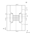
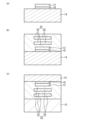
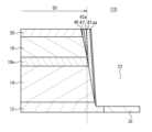
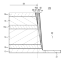
図1は、実施例1に係る弾性波デバイス100の平面図である。図2(a)は、図1のA-A断面図、図2(b)は、図1のB-B断面図である。図1では、主に下部電極12、圧電層14、および上部電極16を図示している。また、図の明瞭化のために、図1では、共振領域50にハッチングを付し、貫通孔22を他より太い線で図示し、図2(b)では、上部電極16等の側面上に形成された膜については図示を省略している。圧電層14の法線方向をZ方向、圧電層14の平面方向において互いに直交する方向をX方向およびY方向とする。 Figure 1 is a plan view of an acoustic wave device 100 according to a first embodiment. Figure 2(a) is a cross-sectional view taken along line A-A in Figure 1, and Figure 2(b) is a cross-sectional view taken along line B-B in Figure 1. Figure 1 mainly illustrates the lower electrode 12, the piezoelectric layer 14, and the upper electrode 16. For clarity, the resonance region 50 is hatched in Figure 1, the through-holes 22 are illustrated with thicker lines than the rest, and the films formed on the side surfaces of the upper electrode 16, etc. are omitted in Figure 2(b). The normal direction of the piezoelectric layer 14 is the Z direction, and the directions perpendicular to each other in the planar direction of the piezoelectric layer 14 are the X direction and the Y direction.

図1、図2(a)、および図2(b)に示すように、弾性波デバイス100は、下部電極12と圧電層14と上部電極16とを備える圧電薄膜共振器である。基板10上に音響反射膜30が設けられ、音響反射膜30上に圧電層14が設けられている。圧電層14の上面および下面は平坦面である。圧電層14の上下に上部電極16および下部電極12が設けられている。圧電層14の少なくとも一部を挟み下部電極12と上部電極16とが平面視において重なる領域が共振領域50である。共振領域50の平面形状は例えばほぼ矩形である。矩形はほぼ直線の4つの辺を有する。4つの辺のうち一対の辺はほぼY方向に沿って伸び、別の一対の辺はほぼX方向に沿って伸びている。 1, 2(a), and 2(b), the acoustic wave device 100 is a piezoelectric thin-film resonator including a lower electrode 12, a piezoelectric layer 14, and an upper electrode 16. An acoustic reflection film 30 is provided on a substrate 10, and a piezoelectric layer 14 is provided on the acoustic reflection film 30. The upper and lower surfaces of the piezoelectric layer 14 are flat. An upper electrode 16 and a lower electrode 12 are provided above and below the piezoelectric layer 14. The region where the lower electrode 12 and the upper electrode 16 overlap in a planar view, sandwiching at least a portion of the piezoelectric layer 14, is the resonance region 50. The planar shape of the resonance region 50 is, for example, approximately rectangular. The rectangle has four approximately straight sides. Of the four sides, one pair of sides extends approximately along the Y direction, and another pair of sides extends approximately along the X direction.

基板10は、例えばシリコン基板、サファイア基板、アルミナ基板、スピネル基板、石英基板、水晶基板、ガラス基板、セラミック基板、またはGaAs基板等である。圧電層14は、例えば単結晶ニオブ酸リチウム層または単結晶タンタル酸リチウム層である。圧電層14の厚さは例えば200nm~1000nm程度である。下部電極12および上部電極16は、例えばルテニウム(Ru)、クロム(Cr)、アルミニウム(Al)、チタン(Ti)、銅(Cu)、モリブデン(Mo)、タングステン(W)、タンタル(Ta)、白金(Pt)、ロジウム(Rh)、またはイリジウム(Ir)等の単層膜またはこれらの積層膜である。下部電極12および上部電極16の厚さは例えば20nm~150nm程度である。下部電極12および上部電極16は、例えば圧電層14の構成元素と異なる金属元素により形成されている。 The substrate 10 is, for example, a silicon substrate, a sapphire substrate, an alumina substrate, a spinel substrate, a quartz substrate, a crystal substrate, a glass substrate, a ceramic substrate, a GaAs substrate, or the like. The piezoelectric layer 14 is, for example, a single crystal lithium niobate layer or a single crystal lithium tantalate layer. The thickness of the piezoelectric layer 14 is, for example, about 200 nm to 1000 nm. The lower electrode 12 and the upper electrode 16 are, for example, a single layer film of ruthenium (Ru), chromium (Cr), aluminum (Al), titanium (Ti), copper (Cu), molybdenum (Mo), tungsten (W), tantalum (Ta), platinum (Pt), rhodium (Rh), iridium (Ir), or the like, or a laminated film of these. The thickness of the lower electrode 12 and the upper electrode 16 is, for example, about 20 nm to 150 nm. The lower electrode 12 and the upper electrode 16 are, for example, formed of a metal element different from the constituent element of the piezoelectric layer 14.

下部電極12と上部電極16との間に高周波電力が印加されると、共振領域50内の圧電層14に弾性波が励振する。弾性波の波長λは圧電層14の厚さのほぼ2倍である。圧電層14が単結晶ニオブ酸リチウム層または単結晶タンタル酸リチウム層である場合、圧電層14には弾性波の変位がZ方向にほぼ直交する方向(すなわち厚さに対して歪み方向)に振動する弾性波が励振される。この振動を厚みすべり振動という。厚みすべり振動の変位の最も大きい方向(厚みすべり振動の変位方向)を厚みすべり振動の振動方向60とする。ここでは、厚みすべり振動の振動方向60はY方向である。下部電極12および上部電極16は、共振領域50から厚みすべり振動の振動方向60と同じY方向に引き出されている。 When high-frequency power is applied between the lower electrode 12 and the upper electrode 16, an elastic wave is excited in the piezoelectric layer 14 in the resonance region 50. The wavelength λ of the elastic wave is approximately twice the thickness of the piezoelectric layer 14. When the piezoelectric layer 14 is a single-crystal lithium niobate layer or a single-crystal lithium tantalate layer, an elastic wave is excited in the piezoelectric layer 14 in which the displacement of the elastic wave vibrates in a direction approximately perpendicular to the Z direction (i.e., the direction of distortion relative to the thickness). This vibration is called thickness-slide vibration. The direction in which the displacement of the thickness-slide vibration is greatest (the displacement direction of the thickness-slide vibration) is set to the vibration direction 60 of the thickness-slide vibration. Here, the vibration direction 60 of the thickness-slide vibration is the Y direction. The lower electrode 12 and the upper electrode 16 are drawn out from the resonance region 50 in the Y direction, which is the same as the vibration direction 60 of the thickness-slide vibration.

音響反射膜30は、音響インピーダンスの低い膜32と音響インピーダンスの高い膜34とを有する。共振領域50において音響インピーダンスの低い膜32と高い膜34は交互に設けられている。共振領域50における膜32および34の厚さは例えばそれぞれほぼλ/4(λは弾性波の波長)である。これにより、音響反射膜30は弾性波を反射する。膜32と膜34の積層数は任意に設定できる。音響反射膜30は、音響特性の異なる少なくとも2種類の層が間隔をあけて積層されていればよい。また、基板10が音響反射膜30の音響特性の異なる少なくとも2種類の層のうちの1層であってもよい。例えば、音響反射膜30は、基板10中に音響インピーダンスの異なる膜が1層設けられている場合でもよい。平面視において、膜32および膜34の積層部分は共振領域50に重なり共振領域50と同じ大きさまたは共振領域50より大きい。膜32および膜34の積層部分を平面視にて共振領域50より大きくすることで、共振領域50から斜め方向に漏れた弾性波を音響反射膜30で反射させることができ、特性の劣化を抑制することができる。音響インピーダンスの低い膜32は例えば酸化シリコン(SiO)膜であり、高い膜34は例えばタングステン(W)膜である。 The acoustic reflection film 30 has a film 32 with a low acoustic impedance and a film 34 with a high acoustic impedance. The films 32 with a low acoustic impedance and the films 34 with a high acoustic impedance are alternately arranged in the resonance region 50. The thicknesses of the films 32 and 34 in the resonance region 50 are, for example, approximately λ/4 (λ is the wavelength of the elastic wave). This allows the acoustic reflection film 30 to reflect the elastic wave. The number of layers of the films 32 and 34 can be set arbitrarily. The acoustic reflection film 30 only needs to have at least two types of layers with different acoustic characteristics stacked at intervals. The substrate 10 may be one of the at least two types of layers with different acoustic characteristics of the acoustic reflection film 30. For example, the acoustic reflection film 30 may have one layer of a film with a different acoustic impedance in the substrate 10. In a plan view, the stacked portion of the films 32 and 34 overlaps the resonance region 50 and is the same size as the resonance region 50 or larger than the resonance region 50. By making the laminated portion of the film 32 and the film 34 larger than the resonance region 50 in a plan view, the acoustic waves leaking obliquely from the resonance region 50 can be reflected by the acoustic reflecting film 30, thereby suppressing deterioration of characteristics. The film 32 with low acoustic impedance is, for example, a silicon oxide (SiO 2 ) film, and the film 34 with high acoustic impedance is, for example, a tungsten (W) film.

共振領域50において下部電極12と圧電層14の間に挿入膜18が設けられている。挿入膜18は、平面視において共振領域50と同じ大きさまたは共振領域50より大きい。挿入膜18は、下部電極12および上部電極16よりも体積抵抗率の高い膜であり、例えば酸化シリコン(SiO)膜である。挿入膜18の厚さは、例えば5nm~20nm程度であり、例えば圧電層14の厚さの10%以下である。圧電層14および上部電極16を覆って保護膜20が設けられている。保護膜20は、絶縁膜であり、例えば酸化シリコン(SiO)膜、窒化シリコン(SiN)膜、または酸化アルミニウム(Al)膜等である。 An insertion film 18 is provided between the lower electrode 12 and the piezoelectric layer 14 in the resonance region 50. The insertion film 18 is the same size as or larger than the resonance region 50 in a plan view. The insertion film 18 is a film having a higher volume resistivity than the lower electrode 12 and the upper electrode 16, for example, a silicon oxide (SiO 2 ) film. The thickness of the insertion film 18 is, for example, about 5 nm to 20 nm, for example, 10% or less of the thickness of the piezoelectric layer 14. A protective film 20 is provided to cover the piezoelectric layer 14 and the upper electrode 16. The protective film 20 is an insulating film, for example, a silicon oxide (SiO 2 ) film, a silicon nitride (SiN) film, an aluminum oxide (Al 2 O 3 ) film, or the like.

圧電層14には、X方向において共振領域50を挟み、Y方向において共振領域50に沿った一対の貫通孔22が形成されている。貫通孔22は、下部電極12の一部まで掘り込まれている。一対の貫通孔22それぞれと共振領域50における圧電層14との間の距離はほぼ同じである。貫通孔22は、例えば平面視においてほぼ矩形状をしている。貫通孔22が設けられることで、共振領域50に励振された弾性波が外部に漏れることが抑制される。 A pair of through holes 22 are formed in the piezoelectric layer 14, sandwiching the resonance region 50 in the X direction and running along the resonance region 50 in the Y direction. The through holes 22 are dug into a portion of the lower electrode 12. The distance between each of the pair of through holes 22 and the piezoelectric layer 14 in the resonance region 50 is approximately the same. The through holes 22 are, for example, approximately rectangular in plan view. The provision of the through holes 22 prevents the elastic waves excited in the resonance region 50 from leaking to the outside.

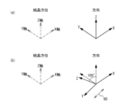
ここで、圧電層14がニオブ酸リチウム層またはタンタル酸リチウム層である場合の圧電層14の結晶方位と、厚みすべり振動の振動方向60と、の関係について説明する。まず、オイラー角(φ、θ、ψ)の定義について説明する。右手系のXYZ座標系において、圧電層14の上面の法線方向をZ方向とし、Z方向に直交する方向であって圧電層14の上面の面方向で互いに直交する方向をX方向およびY方向とする。X方向、Y方向、およびZ方向をそれぞれ結晶方位のX軸方向、Y軸方向、およびZ軸方向とする。次に、Z方向を中心に+X方向から+Y方向に角度φ回転させる。角度φ回転後のX方向を中心に+Y方向から+Z方向に角度θ回転させる。角度θ回転後のZ方向を中心に+X方向から+Y方向に角度ψ回転させる。このように回転させたときのオイラー角は(φ、θ、ψ)となる。なお、(φ、θ、ψ)を用い表現されるオイラー角は、等価なオイラー角を含む。 Here, the relationship between the crystal orientation of the piezoelectric layer 14 and the vibration direction 60 of the thickness-shear vibration when the piezoelectric layer 14 is a lithium niobate layer or a lithium tantalate layer will be described. First, the definition of Euler angles (φ, θ, ψ) will be described. In a right-handed XYZ coordinate system, the normal direction of the upper surface of the piezoelectric layer 14 is the Z direction, and the directions perpendicular to the Z direction and perpendicular to each other in the surface direction of the upper surface of the piezoelectric layer 14 are the X direction and the Y direction. The X direction, the Y direction, and the Z direction are the X-axis direction, the Y-axis direction, and the Z-axis direction of the crystal orientation, respectively. Next, rotate from the +X direction to the +Y direction by an angle φ around the Z direction. Rotate from the +Y direction to the +Z direction by an angle θ around the X direction after the angle φ rotation. Rotate from the +X direction to the +Y direction by an angle ψ around the Z direction after the angle θ rotation. The Euler angles when rotated in this way are (φ, θ, ψ). Note that the Euler angles expressed using (φ, θ, ψ) include equivalent Euler angles.

図3(a)および図3(b)は、圧電層14がニオブ酸リチウム層またはタンタル酸リチウム層である場合における圧電層14の結晶方位と厚みすべり振動の振動方向60との関係を示す図である。図3(a)および図3(b)における左側の破線矢印は圧電層14の結晶軸の方位を示す。右側の実線矢印は図1、図2(a)、および図2(b)のX方向、Y方向、およびZ方向に対応する。図3(a)に示すように、+X方向、+Y方向、および+Z方向をそれぞれ圧電層14の結晶方位の+X軸方向、+Y軸方向、および+Z軸方向とする。図3(b)に示すように、図3(a)の状態から、X方向を中心にYZ平面上において+Y方向および+Z方向を+Y方向から-Z方向に105°回転させる。このように回転させると、結晶方位の+Z軸方向を+Y軸方向に向かって105°回転させた方向が+Z方向となる。このとき、Y方向が厚みすべり振動の振動方向60となる。オイラー角では(0°、-105°、0°)となる。なお、上記と同様の方法によって導出されるオイラー角が(0°、-105°、90°)の場合には、X方向が厚みすべり振動の振動方向60となる。オイラー角の各角度は±5°の範囲内を許容し、±1°の範囲内であることがより好ましい。 3(a) and 3(b) are diagrams showing the relationship between the crystal orientation of the piezoelectric layer 14 and the vibration direction 60 of the thickness-shear vibration when the piezoelectric layer 14 is a lithium niobate layer or a lithium tantalate layer. The dashed arrows on the left side in FIG. 3(a) and FIG. 3(b) indicate the orientation of the crystal axis of the piezoelectric layer 14. The solid arrows on the right side correspond to the X-direction, Y-direction, and Z-direction in FIG. 1, FIG. 2(a), and FIG. 2(b). As shown in FIG. 3(a), the +X-direction, +Y-direction, and +Z-direction are respectively the +X-axis direction, +Y-axis direction, and +Z-axis direction of the crystal orientation of the piezoelectric layer 14. As shown in FIG. 3(b), from the state of FIG. 3(a), the +Y-direction and +Z-direction are rotated 105° from the +Y-direction to the -Z-direction on the YZ plane around the X-direction. When rotated in this way, the direction in which the +Z-axis direction of the crystal orientation is rotated 105° toward the +Y-axis direction becomes the +Z direction. In this case, the Y direction is the vibration direction 60 of the thickness-shear vibration. In terms of Euler angles, they are (0°, -105°, 0°). When the Euler angles derived by the same method as above are (0°, -105°, 90°), the X direction is the vibration direction 60 of the thickness-shear vibration. Each Euler angle is allowed to be within a range of ±5°, and it is more preferable that it is within a range of ±1°.

[シミュレーション]
図4は、シミュレーションに用いたモデルAの断面図である。図4に示すように、モデルAは、基板10上に音響インピーダンスの低い膜32と高い膜34を有する音響反射膜30を備える。音響反射膜30上に圧電層14が設けられている。圧電層14を挟むように下部電極12と上部電極16が設けられている。これにより、共振領域50が形成されている。共振領域50の側方に位置する貫通孔22が圧電層14に設けられている。
[simulation]
Fig. 4 is a cross-sectional view of model A used in the simulation. As shown in Fig. 4, model A includes an acoustic reflection film 30 having a film 32 with low acoustic impedance and a film 34 with high acoustic impedance on a substrate 10. A piezoelectric layer 14 is provided on the acoustic reflection film 30. A lower electrode 12 and an upper electrode 16 are provided to sandwich the piezoelectric layer 14. This forms a resonance region 50. A through hole 22 located on the side of the resonance region 50 is provided in the piezoelectric layer 14.

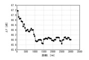
モデルAに対して、貫通孔22と共振領域50との間の距離Lが異なるときのΔYについてシミュレーションをした。ΔYは、アドミッタンス|Y|の周波数特性のシミュレーション結果から、共振周波数でのアドミッタンス|Y|の絶対値と反共振周波数でのアドミッタンス|Y|の絶対値との差を求めることで算出した。シミュレーション条件は以下である。
基板10:シリコン基板
音響インピーダンスの低い膜32:共振領域50での厚さが150nmの酸化シリコン(SiO)膜
音響インピーダンスの高い膜34:共振領域50での厚さが115nmのタングステン(W)膜
下部電極12:厚さ44nmのアルミニウム(Al)膜
圧電層14:厚さ310nmの単結晶ニオブ酸リチウム(LiNbO)層
上部電極16:厚さ44nmのアルミニウム(Al)膜
貫通孔22の幅W:1.0μm
弾性波の波長λ:620nm
A simulation was performed for ΔY when the distance L between the through hole 22 and the resonance region 50 was different for model A. ΔY was calculated by obtaining the difference between the absolute value of admittance |Y| at the resonance frequency and the absolute value of admittance |Y| at the anti-resonance frequency from the simulation results of the frequency characteristic of admittance |Y|. The simulation conditions were as follows.
Substrate 10: silicon substrate Low acoustic impedance film 32: silicon oxide (SiO 2 ) film having a thickness of 150 nm in the resonance region 50 High acoustic impedance film 34: tungsten (W) film having a thickness of 115 nm in the resonance region 50 Lower electrode 12: aluminum (Al) film having a thickness of 44 nm Piezoelectric layer 14: single crystal lithium niobate (LiNbO 3 ) layer having a thickness of 310 nm Upper electrode 16: aluminum (Al) film having a thickness of 44 nm Width W of through hole 22: 1.0 μm
Elastic wave wavelength λ: 620 nm

図5は、モデルAにおける貫通孔22と共振領域50との間の距離Lに対するΔYのシミュレーション結果である。図5に示すように、距離Lが1000nm程度までは、距離Lが大きくなるに連れてΔYは小さくなった。距離Lが1000nmを超えると、ΔYの低下は飽和して、ΔYはほぼ同じ大きさとなった。この結果から、デバイス特性の劣化を抑制しつつデバイスの大型化を抑制する点から、貫通孔22は、共振領域50からの距離Lが1.0μm以下の位置に形成されることが好ましいことが言える。言い換えると、貫通孔22は、共振領域50からの距離Lが1.6λ以下の位置に形成されることが好ましいことが言える。 Figure 5 shows the simulation results of ΔY versus distance L between the through
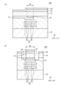
 hole 22 and the resonance region 50 in model A. As shown in Figure 5, ΔY decreased as distance L increased, up to about 1000 nm. When distance L exceeded 1000 nm, the decrease in ΔY saturated, and ΔY remained almost constant. From this result, it can be said that in order to suppress deterioration of device characteristics while suppressing an increase in device size, it is preferable that the through hole 22 be formed at a position where the distance L from the resonance region 50 is 1.0 μm or less. In other words, it can be said that it is preferable that the through hole 22 be formed at a position where the distance L from the resonance region 50 is 1.6 λ or less.

[製造方法]
図6(a)から図7(b)は、実施例1に係る弾性波デバイス100の製造方法を示す断面図である。図6(a)から図7(b)は、図1のB-B間に相当する箇所の断面図である。図6(a)に示すように、圧電層14として圧電基板を準備する。圧電層14上に挿入膜18と下部電極12を形成する。挿入膜18および下部電極12は、例えばスパッタリング法、真空蒸着法、またはCVD(Chemical Vapor Deposition)法を用いて成膜した後、例えばフォトリソグラフィ法およびエッチング法を用いて所望の形状にパターニングすることで形成する。挿入膜18および下部電極12はリフトオフ法を用いて形成してもよい。
[Production method]
6(a) to 7(b) are cross-sectional views showing a method for manufacturing the acoustic wave device 100 according to the first embodiment. FIGS. 6(a) to 7(b) are cross-sectional views of a portion corresponding to the section B-B in FIG. 1. As shown in FIG. 6(a), a piezoelectric substrate is prepared as the piezoelectric layer 14. An insertion film 18 and a lower electrode 12 are formed on the piezoelectric layer 14. The insertion film 18 and the lower electrode 12 are formed by forming a film using, for example, a sputtering method, a vacuum deposition method, or a CVD (Chemical Vapor Deposition) method, and then patterning the film into a desired shape using, for example, a photolithography method and an etching method. The insertion film 18 and the lower electrode 12 may be formed using a lift-off method.

図6(b)に示すように、圧電層14上に挿入膜18および下部電極12を覆って音響反射膜30を形成する。音響反射膜30は、音響インピーダンスの低い膜32と高い膜34を交互に成膜し、音響インピーダンスの高い膜34に関しては所望の形状にパターニングすることにより形成する。音響インピーダンスの低い膜32と高い膜34の成膜は例えばスパッタリング法またはCVD法を用い、パターニングは例えばフォトリソグラフィ法およびエッチング法を用いる。その後、音響反射膜30の上面を例えばCMP(Chemical Mechanical Polishing)法を用い平坦化する。 As shown in FIG. 6(b), an acoustic reflection film 30 is formed on the piezoelectric layer 14, covering the insertion film 18 and the lower electrode 12. The acoustic reflection film 30 is formed by alternately depositing films 32 with low acoustic impedance and films 34 with high acoustic impedance, and patterning the film 34 with high acoustic impedance into a desired shape. The films 32 with low acoustic impedance and the film 34 with high acoustic impedance are deposited, for example, by sputtering or CVD, and patterned, for example, by photolithography and etching. The upper surface of the acoustic reflection film 30 is then planarized, for example, by CMP (Chemical Mechanical Polishing).

図6(c)に示すように、音響反射膜30を基板10に接合させる。接合には例えば表面活性化法を用いる。基板10と音響反射膜30との間にシリコン膜等の接合層を設けてもよい。次いで、圧電層14を所望の厚さに薄膜化する。薄膜化には、例えば研削法および/またはCMP法を用いる。例えば研削法を用いて圧電層14をほぼ所望の厚さとし、CMP法を用いて上面を平坦化する。これにより、圧電層14の上面は製造誤差程度に平坦面となる。 As shown in FIG. 6(c), the acoustic reflection film 30 is bonded to the substrate 10. For example, a surface activation method is used for bonding. A bonding layer such as a silicon film may be provided between the substrate 10 and the acoustic reflection film 30. Next, the piezoelectric layer 14 is thinned to the desired thickness. For example, a grinding method and/or a CMP method is used for thinning. For example, the piezoelectric layer 14 is made to approximately the desired thickness using a grinding method, and the upper surface is flattened using a CMP method. As a result, the upper surface of the piezoelectric layer 14 becomes flat within the manufacturing error range.

図7(a)に示すように、圧電層14上に上部電極16および保護膜20を形成する。上部電極16および保護膜20は、例えばスパッタリング法、真空蒸着法、またはCVD法を用いて成膜した後、例えばフォトリソグラフィ法およびエッチング法を用いて所望の形状にパターニングすることで形成する。上部電極16はリフトオフ法を用いて形成してもよい。圧電層14の少なくとも一部を挟んで下部電極12と上部電極16が平面視にて重なる共振領域50が形成される。 As shown in FIG. 7(a), an upper electrode 16 and a protective film 20 are formed on the piezoelectric layer 14. The upper electrode 16 and the protective film 20 are formed by depositing the film using, for example, a sputtering method, a vacuum deposition method, or a CVD method, and then patterning the film into a desired shape using, for example, a photolithography method and an etching method. The upper electrode 16 may be formed using a lift-off method. A resonance region 50 is formed in which the lower electrode 12 and the upper electrode 16 overlap in a planar view, sandwiching at least a portion of the piezoelectric layer 14 between them.

図7(b)に示すように、共振領域50の側方における圧電層14を除去して、共振領域50に沿った貫通孔22を圧電層14に形成する。圧電層14の除去は例えばフォトリソグラフィ法およびエッチング法を用いる。例えば、圧電層14の除去は、ドライエッチング法により行い、例えばアルゴン(Ar)ガスを用いたイオンミリング法により行う。このときに、圧電層14を貫通する貫通孔22が確実に形成されるようにオーバーエッチングをする。このため、挿入膜18および下部電極12もエッチングされる。以上により、実施例1に係る弾性波デバイス100が形成される。 As shown in FIG. 7(b), the
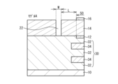
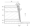
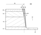
 piezoelectric layer 14 on the sides of the resonance region 50 is removed to form through-holes 22 in the piezoelectric layer 14 along the resonance region 50. The piezoelectric layer 14 is removed by, for example, photolithography and etching. For example, the piezoelectric layer 14 is removed by dry etching, for example, ion milling using argon (Ar) gas. At this time, over-etching is performed to ensure that the through-holes 22 penetrating the piezoelectric layer 14 are formed. For this reason, the insertion film 18 and the lower electrode 12 are also etched. In this manner, the acoustic wave device 100 according to the first embodiment is formed.

[貫通孔近傍]
図8は、実施例1における貫通孔22近傍の断面図である。図8に示すように、保護膜20の側面上に保護膜20の材料を含む膜40が形成されている。上部電極16の側面上から膜40の側面上にかけて上部電極16の材料を含む膜41が形成されている。圧電層14の側面上から膜41の側面上にかけて圧電層14の材料を含む膜42が形成されている。挿入膜18の側面上から膜42の側面上にかけて挿入膜18の材料を含む膜43が形成されている。下部電極12の側面上から膜43の側面上にかけて下部電極12の材料を含む膜44が形成されている。膜40、41、42、43、44は、貫通孔22を形成するときに付着した付着膜であるため、規則的な結晶構造状態を取らない、つまりアモルファスの割合が多く含まれる。
[Via the through hole]
8 is a cross-sectional view of the vicinity of the through hole 22 in the first embodiment. As shown in FIG. 8, a film 40 containing the material of the protective film 20 is formed on the side of the protective film 20. A film 41 containing the material of the upper electrode 16 is formed from the side of the upper electrode 16 to the side of the film 40. A film 42 containing the material of the piezoelectric layer 14 is formed from the side of the piezoelectric layer 14 to the side of the film 41. A film 43 containing the material of the insertion film 18 is formed from the side of the insertion film 18 to the side of the film 42. A film 44 containing the material of the lower electrode 12 is formed from the side of the lower electrode 12 to the side of the film 43. The films 40, 41, 42, 43, and 44 are attached films that are attached when the through hole 22 is formed, so they do not have a regular crystalline structure, that is, they contain a large proportion of amorphous.

貫通孔22と共振領域50における圧電層14との間の最大の距離Lは1.0μm以下となっている。これにより、図5のように、デバイス特性の劣化を抑制しつつデバイスの大型化を抑制することができる。デバイス特性の劣化を抑制する点から、距離Lは0.8μm以下が好ましく、0.5μm以下がより好ましく、0.2μm以下が更に好ましい。 The maximum distance L between the through hole 22 and the piezoelectric layer 14 in the resonance region 50 is 1.0 μm or less. This makes it possible to suppress the device from becoming larger while suppressing deterioration of the device characteristics, as shown in FIG. 5. From the viewpoint of suppressing deterioration of the device characteristics, the distance L is preferably 0.8 μm or less, more preferably 0.5 μm or less, and even more preferably 0.2 μm or less.

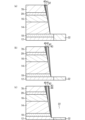
膜40、41、42、43、および44が形成される過程について図を用いて説明する。図9(a)から図10(c)は、実施例1における貫通孔22の形成工程を示す断面図である。図9(a)に示すように、上部電極16上にフォトレジストからなるマスク層70を形成する。マスク層70は、上部電極16の端よりも内側に位置して形成される。 The process of forming the films 40, 41, 42, 43, and 44 will be described with reference to the drawings. FIGS. 9(a) to 10(c) are cross-sectional views showing the process of forming the through-hole 22 in Example 1. As shown in FIG. 9(a), a mask layer 70 made of photoresist is formed on the upper electrode 16. The mask layer 70 is formed to be located inside the edge of the upper electrode 16.

図9(b)に示すように、マスク層70をマスクとして保護膜20および上部電極16をエッチングする。エッチングは、ドライエッチング法を用い、例えばArガスを用いたイオンミリング法を用いる。保護膜20のエッチングの際に除去された材料が保護膜20の側面およびマスク層70の側面に付着し、保護膜20の材料を含む膜40が保護膜20の側面上からマスク層70の側面上にかけて形成される。また、上部電極16のエッチングの際に除去された材料が上部電極16の側面および膜40の側面に付着し、上部電極16の材料を含む膜41が上部電極16の側面上から膜40の側面上にかけて形成される。 As shown in FIG. 9B, the protective film 20 and the upper electrode 16 are etched using the mask layer 70 as a mask. The etching is performed by a dry etching method, for example, an ion milling method using Ar gas. The material removed during the etching of the protective film 20 adheres to the side surfaces of the protective film 20 and the mask layer 70, and a film 40 containing the material of the protective film 20 is formed from the side surfaces of the protective film 20 to the side surfaces of the mask layer 70. The material removed during the etching of the upper electrode 16 adheres to the side surfaces of the upper electrode 16 and the film 40, and a film 41 containing the material of the upper electrode 16 is formed from the side surfaces of the upper electrode 16 to the side surfaces of the film 40.

図10(a)に示すように、保護膜20および上部電極16のエッチングに続いて、マスク層70をマスクとして圧電層14をエッチングする。エッチングは、上述のように、ドライエッチング法を用い、例えばArガスを用いたイオンミリング法を用いる。圧電層14のエッチングの際に除去された材料が圧電層14の側面および膜41の側面に付着し、圧電層14の材料を含む膜42が圧電層14の側面上から膜41の側面上にかけて形成される。 As shown in FIG. 10(a), following the etching of the protective film 20 and the upper electrode 16, the piezoelectric layer 14 is etched using the mask layer 70 as a mask. As described above, the etching is performed by dry etching, for example, ion milling using Ar gas. The material removed during the etching of the piezoelectric layer 14 adheres to the side surfaces of the piezoelectric layer 14 and the side surfaces of the film 41, and a film 42 containing the material of the piezoelectric layer 14 is formed from the side surfaces of the piezoelectric layer 14 to the side surfaces of the film 41.

図10(b)に示すように、圧電層14のエッチングに続いて、マスク層70をマスクとして挿入膜18をエッチングする。エッチングは、上述のように、ドライエッチング法を用い、例えばArガスを用いたイオンミリング法を用いる。挿入膜18のエッチングの際に除去された材料が挿入膜18の側面および膜42の側面に付着し、挿入膜18の材料を含む膜43が挿入膜18の側面上から膜42の側面上にかけて形成される。 As shown in FIG. 10(b), following the etching of the piezoelectric layer 14, the insertion film 18 is etched using the mask layer 70 as a mask. As described above, the etching is performed by dry etching, for example, ion milling using Ar gas. The material removed during the etching of the insertion film 18 adheres to the side surfaces of the insertion film 18 and the side surfaces of the film 42, and a film 43 containing the material of the insertion film 18 is formed from the side surfaces of the insertion film 18 to the side surfaces of the film 42.

図10(c)に示すように、挿入膜18のエッチングに続いて、マスク層70をマスクとして下部電極12をエッチングする。下部電極12までエッチングをするのは、貫通孔22が圧電層14を貫通していない場合ではデバイス特性が劣化するため、貫通孔22が圧電層14を確実に貫通するようにオーバーエッチングをするためである。エッチングは、上述のように、ドライエッチング法を用い、例えばArガスを用いたイオンミリング法を用いる。下部電極12のエッチングの際に除去された材料が下部電極12の側面および膜43の側面に付着し、下部電極12の材料を含む膜44が下部電極12の側面上から膜43の側面上にかけて形成される。 As shown in FIG. 10(c), following the etching of the insertion film 18, the lower electrode 12 is etched using the mask layer 70 as a mask. The reason for etching down to the lower electrode 12 is to ensure that the through-holes 22 penetrate the piezoelectric layer 14 by over-etching, since device characteristics would be degraded if the through-holes 22 did not penetrate the piezoelectric layer 14. As described above, the etching is performed by dry etching, for example, ion milling using Ar gas. The material removed during the etching of the lower electrode 12 adheres to the side of the lower electrode 12 and the side of the film 43, and a film 44 containing the material of the lower electrode 12 is formed from the side of the lower electrode 12 to the side of the film 43.

[実験]
実施例1において、音響インピーダンスの低い膜32、下部電極12、挿入膜18、圧電層14、上部電極16、および保護膜20を以下の材料および膜厚で形成し、Arガスを用いたイオンミリング法によって貫通孔22を形成した。貫通孔22を形成する際のオーバーエッチングによって下部電極12は22nm程度掘り込まれるようにした。
音響インピーダンスの低い膜32:酸化シリコン膜
下部電極12:厚さが44nmのアルミニウム膜
挿入膜18:厚さが20nmの酸化シリコン膜
圧電層14:厚さが310nmのニオブ酸リチウム層
上部電極16:厚さが44nmのアルミニウム膜
保護膜20:厚さが20nmの酸化シリコン膜
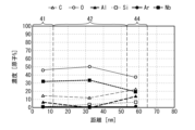
このときに、図8の矢印Aで示す箇所における膜41、42、43、44の組成分析を行った。組成分析はエネルギー分散型X線分光法(EDX)によって行った。
[experiment]
In Example 1, the low acoustic impedance film 32, the lower electrode 12, the insertion film 18, the piezoelectric layer 14, the upper electrode 16, and the protective film 20 were formed from the following materials and with the following thicknesses, and the through hole 22 was formed by ion milling using Ar gas. The lower electrode 12 was dug down by about 22 nm by over-etching when forming the through hole 22.
Low acoustic impedance film 32: silicon oxide film Lower electrode 12: aluminum film with a thickness of 44 nm Insertion film 18: silicon oxide film with a thickness of 20 nm Piezoelectric layer 14: lithium niobate layer with a thickness of 310 nm Upper electrode 16: aluminum film with a thickness of 44 nm Protective film 20: silicon oxide film with a thickness of 20 nm At this time, composition analysis was performed on films 41, 42, 43, and 44 at the location indicated by arrow A in Fig. 8. The composition analysis was performed by energy dispersive X-ray spectroscopy (EDX).

図11は、実施例1における組成分析の実験結果を示す図である。図11において、横軸は上部電極16の側面の位置を原点0としたときの矢印Aの方向における上部電極16の側面からの距離であり、縦軸は濃度である。表1は、実施例1における組成分析の実験結果を示す表である。

Figure 2025041295000002
Fig. 11 is a diagram showing the experimental results of the composition analysis in Example 1. In Fig. 11, the horizontal axis represents the distance from the side surface of the upper electrode 16 in the direction of arrow A when the position of the side surface of the upper electrode 16 is set as the origin 0, and the vertical axis represents the concentration. Table 1 is a table showing the experimental results of the composition analysis in Example 1.
Figure 2025041295000002

図11および表1に示すように、膜41はアルミニウム(Al)を含んでいる。このことから、膜41は、上部電極16のエッチングの際に除去された材料が付着したものであることが分かる。なお、炭素(C)はフォトレジストからなるマスク層70がエッチングされたことで取り込まれたものと考えられる。酸素(O)は保護膜20および圧電層14のエッチングの際に除去された材料を含む膜40、42に含まれる酸素が入り込んだものと考えられる。シリコン(Si)は膜40に含まれるシリコンが入り込んだものと考えられる。アルゴン(Ar)はイオンミリング法で用いたガスが取り込まれたものと考えられる。ニオブ(Nb)は膜42に含まれるニオブが入り込んだものと考えられる。 As shown in FIG. 11 and Table 1, the film 41 contains aluminum (Al). This shows that the material removed during etching of the upper electrode 16 adheres to the film 41. Carbon (C) is believed to have been incorporated by etching the mask layer 70 made of photoresist. Oxygen (O) is believed to have been incorporated from oxygen contained in the films 40 and 42, which contain materials removed during etching of the protective film 20 and the piezoelectric layer 14. Silicon (Si) is believed to have been incorporated from silicon contained in the film 40. Argon (Ar) is believed to have been incorporated from the gas used in the ion milling method. Niobium (Nb) is believed to have been incorporated from niobium contained in the film 42.

膜42は、アルミニウムを含まず、ニオブの濃度が他の膜41、43、44より高くかつシリコンの濃度が膜43より低くなっている。例えば、膜42のニオブの濃度は、膜44のニオブの濃度の1.3倍以上であり、また1.5倍以上となっている。このことから、膜42は、圧電層14のエッチングの際に除去された材料が付着したものであることが分かる。なお、炭素はマスク層70がエッチングされることで取り込まれたものと考えられる。酸素は圧電層14がエッチングされた際に圧電層14の構成元素である酸素が取り込まれたために濃度が高くなっていると考えられる。シリコンは膜43に含まれるシリコンが入り込んだものと考えられる。アルゴンはイオンミリング法で用いたガスが取り込まれたものと考えられる。なお、膜42に圧電層14の構成元素であるリチウム(Li)が含まれていなかったのは、リチウムは軽いために取り込まれ難かったためと考えられる。 Film 42 does not contain aluminum, has a higher niobium concentration than the other films 41, 43, and 44, and a lower silicon concentration than film 43. For example, the niobium concentration of film 42 is 1.3 times or more, and 1.5 times or more, the niobium concentration of film 44. This shows that film 42 is formed by the attachment of material removed during etching of piezoelectric layer 14. It is believed that carbon was incorporated by etching mask layer 70. It is believed that oxygen has a high concentration because oxygen, a constituent element of piezoelectric layer 14, was incorporated when piezoelectric layer 14 was etched. It is believed that silicon was incorporated from film 43. It is believed that argon was incorporated from the gas used in the ion milling method. It is believed that lithium (Li), a constituent element of piezoelectric layer 14, was not included in film 42 because lithium is light and difficult to incorporate.

膜43は、アルミニウムを含まず、シリコンの濃度が他の膜41、42、44より高くかつニオブの濃度が膜42より低くなっている。例えば、膜43のシリコンの濃度は、膜42のシリコンの濃度の1.8倍以上であり、また2.0倍以上となっている。膜43のニオブの濃度は、膜42のニオブの濃度の0.8倍以下であり、また0.7倍以下となっている。このことから、膜43は、挿入膜18のエッチングの際に除去された材料が付着したものであることが分かる。なお、炭素はマスク層70がエッチングされることで取り込まれたものと考えられる。酸素は挿入膜18がエッチングされた際に挿入膜18の構成元素である酸素が取り込まれたために濃度が高くなっていると考えられる。アルゴンはイオンミリング法で用いたガスが取り込まれたものと考えられる。ニオブは膜42に含まれるニオブが入り込んだものと考えられる。 The film 43 does not contain aluminum, and has a higher silicon concentration than the other films 41, 42, and 44, and a lower niobium concentration than the film 42. For example, the silicon concentration of the film 43 is 1.8 times or more, or 2.0 times or more, than the silicon concentration of the film 42. The niobium concentration of the film 43 is 0.8 times or less, or 0.7 times or less, than the niobium concentration of the film 42. From this, it can be seen that the film 43 is made of the material removed during the etching of the insertion film 18. It is considered that the carbon was taken in by etching the mask layer 70. It is considered that the oxygen concentration is high because oxygen, which is a constituent element of the insertion film 18, was taken in when the insertion film 18 was etched. It is considered that the argon was taken in by the gas used in the ion milling method. It is considered that the niobium was taken in by the niobium contained in the film 42.

膜44はアルミニウムを含んでいる。このことから、膜44は、下部電極12のエッチングの際に除去された材料が付着したものであることが分かる。なお、炭素はマスク層70がエッチングされることで入り込んだものと考えられる。酸素およびシリコンは音響インピーダンスの低い膜32がエッチングされることで取り込まれたものと、膜43に含まれる酸素が入り込んだものと考えられる。アルゴンはイオンミリング法で用いたガスが取り込まれたものと考えられる。ニオブは膜42、43に含まれるニオブが入り込んだものと考えられる。 Film 44 contains aluminum. This shows that film 44 is formed by the adhesion of material removed during etching of lower electrode 12. The carbon is believed to have entered as a result of etching mask layer 70. The oxygen and silicon are believed to have been introduced as a result of etching film 32, which has a low acoustic impedance, and as a result of the oxygen contained in film 43 entering the film. The argon is believed to have been introduced as a result of the gas used in the ion milling method. The niobium is believed to have entered as a result of the niobium contained in films 42 and 43 entering the film.

膜41、42、43、および44の厚さは、例えば上部電極16、圧電層14、挿入膜18、および下部電極12のエッチング量に対応する。例えば、圧電層14が上部電極16、挿入膜18、および下部電極12より厚い場合、膜42は膜41、43、および44より厚くなる。上部電極16の厚さが挿入膜18の厚さおよび下部電極12の掘り込み量より大きい場合、膜41は膜43および膜44より厚くなる。挿入膜18の厚さと下部電極12の掘り込み量が同程度の大きさである場合、膜43と膜44の厚さはほぼ同じになる。 The thicknesses of films 41, 42, 43, and 44 correspond to the amount of etching of, for example, the top electrode 16, the piezoelectric layer 14, the insertion film 18, and the bottom electrode 12. For example, if the piezoelectric layer 14 is thicker than the top electrode 16, the insertion film 18, and the bottom electrode 12, then film 42 will be thicker than films 41, 43, and 44. If the thickness of the top electrode 16 is greater than the thickness of the insertion film 18 and the amount of recessing of the bottom electrode 12, then film 41 will be thicker than films 43 and 44. If the thickness of the insertion film 18 and the amount of recessing of the bottom electrode 12 are of the same order of magnitude, then films 43 and 44 will be approximately the same thickness.

[変形例]
図12は、実施例1の変形例1における貫通孔22近傍の断面図である。図12に示すように、実施例1の変形例1に係る弾性波デバイス110では、共振領域50において、下部電極12と圧電層14の間に挿入膜18は設けられてなく、代わりに、圧電層14と上部電極16の間に挿入膜18aが設けられている。挿入膜18aは、平面視において共振領域50と同じ大きさまたは共振領域50より大きい。このため、挿入膜18aの側面上から膜41の側面上にかけて挿入膜18aの材料を含む膜43aが形成されている。圧電層14の材料を含む膜42は、圧電層14の側面上から膜43aの側面上にかけて形成されている。その他の構成は実施例1と同じであるため説明を省略する。
[Modification]
12 is a cross-sectional view of the vicinity of the through hole 22 in the first modification of the first embodiment. As shown in FIG. 12, in the acoustic wave device 110 according to the first modification of the first embodiment, the insertion film 18 is not provided between the lower electrode 12 and the piezoelectric layer 14 in the resonance region 50, and instead, the insertion film 18a is provided between the piezoelectric layer 14 and the upper electrode 16. The insertion film 18a is the same size as the resonance region 50 or larger than the resonance region 50 in a plan view. Therefore, a film 43a containing the material of the insertion film 18a is formed from the side surface of the insertion film 18a to the side surface of the film 41. The film 42 containing the material of the piezoelectric layer 14 is formed from the side surface of the piezoelectric layer 14 to the side surface of the film 43a. The other configurations are the same as those of the first embodiment, so a description thereof will be omitted.

図13は、実施例1の変形例2における貫通孔22近傍の断面図である。図13に示すように、実施例1の変形例2に係る弾性波デバイス120では、共振領域50において、下部電極12と圧電層14の間に挿入膜18が設けられていることに加え、圧電層14と上部電極16の間に挿入膜18aが設けられている。このため、挿入膜18aの側面上から膜41の側面上にかけて挿入膜18aの材料を含む膜43aが形成されている。圧電層14の材料を含む膜42は、圧電層14の側面上から膜43aの側面上にかけて形成されている。その他の構成は実施例1と同じであるため説明を省略する。 Figure 13 is a cross-sectional view of the vicinity of the through hole 22 in the second modification of the first embodiment. As shown in Figure 13, in the acoustic wave device 120 according to the second modification of the first embodiment, in the resonance region 50, in addition to the insertion film 18 being provided between the lower electrode 12 and the piezoelectric layer 14, the insertion film 18a is provided between the piezoelectric layer 14 and the upper electrode 16. Therefore, a film 43a containing the material of the insertion film 18a is formed from the side surface of the insertion film 18a to the side surface of the film 41. A film 42 containing the material of the piezoelectric layer 14 is formed from the side surface of the piezoelectric layer 14 to the side surface of the film 43a. The other configurations are the same as those in the first embodiment, and therefore will not be described.

[比較例]
図14は、比較例における貫通孔22近傍の断面図である。図14に示すように、比較例に係る弾性波デバイス500では、下部電極12と圧電層14の間に挿入膜18は設けられていない。このため、圧電層14の側面上から膜41の側面上にかけて形成された圧電層14の材料を含む膜42に接して下部電極12の側面上から膜42の側面上にかけて下部電極12の材料を含む膜44が形成されている。すなわち、膜42と膜44の間に、挿入膜18の材料を含む膜43は形成されていない。その他の構成は実施例1と同じであるため説明を省略する。
[Comparative Example]
14 is a cross-sectional view of the vicinity of the through hole 22 in the comparative example. As shown in FIG. 14, in the acoustic wave device 500 according to the comparative example, the insertion film 18 is not provided between the lower electrode 12 and the piezoelectric layer 14. Therefore, the film 44 containing the material of the lower electrode 12 is formed from the side surface of the lower electrode 12 to the side surface of the film 42 in contact with the film 42 containing the material of the piezoelectric layer 14 formed from the side surface of the piezoelectric layer 14 to the side surface of the film 41. In other words, the film 43 containing the material of the insertion film 18 is not formed between the film 42 and the film 44. The other configurations are the same as those in the first embodiment, and therefore will not be described.

[実験]
比較例において、音響インピーダンスの低い膜32、下部電極12、圧電層14、上部電極16、および保護膜20を以下の材料および膜厚で形成し、Arガスを用いたイオンミリング法によって貫通孔22を形成した。貫通孔22を形成する際のオーバーエッチングによって下部電極12は22nm程度掘り込まれるようにした。
音響インピーダンスの低い膜32:酸化シリコン膜
下部電極12:厚さが44nmのアルミニウム膜
圧電層14:厚さが310nmのニオブ酸リチウム層
上部電極16:厚さが44nmのアルミニウム膜
保護膜20:厚さが20nmの酸化シリコン膜
このときに、図14の矢印Aで示す箇所の膜41、42、44の組成分析を行った。組成分析はエネルギー分散型X線分光法(EDX)によって行った。
[experiment]
In the comparative example, the low acoustic impedance film 32, the lower electrode 12, the piezoelectric layer 14, the upper electrode 16, and the protective film 20 were formed from the following materials and with the following thicknesses, and the through-hole 22 was formed by ion milling using Ar gas. The lower electrode 12 was dug down by about 22 nm by over-etching when forming the through-hole 22.
Low acoustic impedance film 32: silicon oxide film Lower electrode 12: aluminum film with a thickness of 44 nm Piezoelectric layer 14: lithium niobate layer with a thickness of 310 nm Upper electrode 16: aluminum film with a thickness of 44 nm Protective film 20: silicon oxide film with a thickness of 20 nm At this time, composition analysis was performed on films 41, 42, and 44 at the location indicated by arrow A in Fig. 14. The composition analysis was performed by energy dispersive X-ray spectroscopy (EDX).

図15は、比較例における組成分析の実験結果を示す図である。図15において、横軸は上部電極16の側面の位置を原点0としたときの矢印Aの方向における上部電極16の側面からの距離であり、縦軸は濃度である。表2は、比較例における組成分析の実験結果を示す表である。

Figure 2025041295000003
Fig. 15 is a diagram showing the experimental results of the composition analysis in the comparative example. In Fig. 15, the horizontal axis represents the distance from the side surface of the upper electrode 16 in the direction of the arrow A when the position of the side surface of the upper electrode 16 is set as the origin 0, and the vertical axis represents the concentration. Table 2 shows the experimental results of the composition analysis in the comparative example.
Figure 2025041295000003

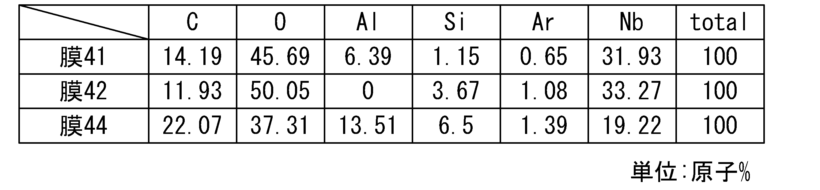
図15および表2に示すように、膜41はアルミニウムを含んでいる。このことから、膜41は、上部電極16のエッチングの際に除去された材料が付着したものであることが分かる。膜42は、アルミニウムを含まず、ニオブの濃度が膜41、44より高くなっている。このことから、膜42は、圧電層14のエッチングの際に除去された材料が付着したものであることが分かる。膜44はアルミニウムを含んでいる。このことから、膜44は、下部電極12のエッチングの際に除去された材料が付着したものであることが分かる。 As shown in FIG. 15 and Table 2, film 41 contains aluminum. This shows that film 41 is made of the material removed during etching of the upper electrode 16. Film 42 does not contain aluminum, and has a higher niobium concentration than films 41 and 44. This shows that film 42 is made of the material removed during etching of the piezoelectric layer 14. Film 44 contains aluminum. This shows that film 44 is made of the material removed during etching of the lower electrode 12.

比較例では、図14のように、膜44は膜42に接して設けられている。膜41は上部電極16のエッチングの際に除去された材料が付着したものであることから導電性を有する。膜44は下部電極12のエッチングの際に除去された材料が付着したものであることから導電性を有する。膜42は、圧電層14のエッチングの際に除去された材料が付着したものであるが、例えばアモルファスとなっていて膜質が悪いために絶縁性が低い。このため、膜42の薄い箇所において膜41と膜44が電気的に接続し、下部電極12と上部電極16が膜41、42、44を介して短絡することがある。短絡が生じるとデバイス特性が劣化してしまう。なお、膜42が厚くなれば絶縁性は高くなるが、膜42は圧電層14の膜厚に対応していて、圧電層14の膜厚は所望の弾性波の波長により決まることから、膜42を厚くするのは難しい。 In the comparative example, as shown in FIG. 14, the film 44 is provided in contact with the film 42. The film 41 is conductive because the material removed during etching of the upper electrode 16 is attached to the film 41. The film 44 is conductive because the material removed during etching of the lower electrode 12 is attached to the film 41. The film 42 is made of the material removed during etching of the piezoelectric layer 14, but it is amorphous and has poor film quality, so it has low insulation. For this reason, the film 41 and the film 44 are electrically connected at a thin portion of the film 42, and the lower electrode 12 and the upper electrode 16 may be short-circuited through the films 41, 42, and 44. If a short circuit occurs, the device characteristics will deteriorate. Note that the thicker the film 42, the higher the insulation, but since the film 42 corresponds to the film thickness of the piezoelectric layer 14, and the film thickness of the piezoelectric layer 14 is determined by the wavelength of the desired elastic wave, it is difficult to make the film 42 thick.

一方、実施例1およびその変形例では、図8、図12、および図13のように、下部電極12および上部電極16の少なくとも一方と圧電層14との間に下部電極12および上部電極16より抵抗率が高い挿入膜18、18aが設けられている。このため、膜44と膜42の間、および、上部電極16の側面と膜42の間、の少なくとも一方に、挿入膜18、18aのエッチングの際に除去された材料が付着した膜である膜43、43aが形成されている。膜44(第1膜)は、下部電極12のエッチングの際に除去された材料が付着した膜であるため、下部電極12に接続していて、図11および表1のように、下部電極12の構成元素であるAlを含んでいる。膜42(第2膜)は、圧電層14のエッチングの際に除去された材料が付着した膜であるため、圧電層14の構成元素であるNbの濃度が膜44より高くなっている。膜43、43a(第3膜)は、挿入膜18、18aのエッチングの際に除去された材料が付着した膜であるため、挿入膜18、18aの構成元素であって圧電層14の構成元素でないSiの濃度が膜42より高くかつ圧電層14の構成元素であって挿入膜18、18aの構成元素でないNbの濃度が膜42より低くなっている。膜43、43aは、下部電極12および上部電極16より抵抗率が高い挿入膜18、18aのエッチング時に除去された材料が付着した膜であることから、上部電極16のエッチング時に除去された材料が付着した膜である膜41および下部電極12のエッチング時に除去された材料が付着した膜である膜44よりも絶縁性が高い。したがって、このような膜43および膜43aの少なくとも一方が、膜41と膜44の間に設けられることで、膜41と膜44の電気的な接続が抑制される。よって、下部電極12と上部電極16の短絡を抑制することができる。 On the other hand, in Example 1 and its modified examples, as shown in Figs. 8, 12, and 13, the insertion films 18, 18a having a higher resistivity than the lower electrode 12 and the upper electrode 16 are provided between at least one of the lower electrode 12 and the upper electrode 16 and the piezoelectric layer 14. Therefore, at least one of the films 44 and 42 and the side of the upper electrode 16 and the film 42 is formed with the film 43, 43a, which is a film with the material removed during etching of the insertion films 18, 18a. The film 44 (first film) is a film with the material removed during etching of the lower electrode 12 attached, so it is connected to the lower electrode 12 and contains Al, which is a constituent element of the lower electrode 12, as shown in Fig. 11 and Table 1. The film 42 (second film) is a film with the material removed during etching of the piezoelectric layer 14 attached, so the concentration of Nb, which is a constituent element of the piezoelectric layer 14, is higher than that of the film 44. Since the films 43 and 43a (third films) are films to which the material removed during etching of the insertion films 18 and 18a is attached, the concentration of Si, which is a constituent element of the insertion films 18 and 18a but not a constituent element of the piezoelectric layer 14, is higher than that of the film 42, and the concentration of Nb, which is a constituent element of the piezoelectric layer 14 but not a constituent element of the insertion films 18 and 18a, is lower than that of the film 42. Since the films 43 and 43a are films to which the material removed during etching of the insertion films 18 and 18a, which have a higher resistivity than the lower electrode 12 and the upper electrode 16, are attached, they have higher insulation properties than the film 41, which is a film to which the material removed during etching of the upper electrode 16 is attached, and the film 44, which is a film to which the material removed during etching of the lower electrode 12 is attached. Therefore, by providing at least one of the films 43 and 43a between the films 41 and 44, the electrical connection between the films 41 and 44 is suppressed. Therefore, it is possible to suppress a short circuit between the lower electrode 12 and the upper electrode 16.

また、実施例1およびその変形例の製造方法では、図7(a)のように、基板10上に下部電極12と圧電層14と上部電極16をこの順に形成し、かつ、下部電極12と圧電層14の間および圧電層14と上部電極16の間の少なくとも一方に挿入膜18、18aを形成する(図12、図13も参照)。図7(b)および図9(a)から図10(c)のように、共振領域50の側方における圧電層14、挿入膜18、18a、および下部電極12をエッチングして、貫通孔22を圧電層14に形成する。このときに、下部電極12のエッチングにより付着した膜44(第1膜)と上部電極16の側面との間に圧電層14のエッチングにより付着した膜42(第2膜)が形成され、上部電極16の側面と膜42の間および膜44と膜42の間の少なくとも一方に挿入膜18、18aのエッチングにより付着した膜43、43a(第3膜)が形成されるようにする(図12、図13も参照)。これにより、膜43および膜43aの少なくとも一方が膜41と膜44の間に設けられるため、膜41と膜44の電気的な接続が抑制され、下部電極12と上部電極16の短絡を抑制することができる。 In the manufacturing method of Example 1 and its modified examples, as shown in Fig. 7(a), the lower electrode 12, the piezoelectric layer 14, and the upper electrode 16 are formed in this order on the substrate 10, and the insertion films 18, 18a are formed at least one between the lower electrode 12 and the piezoelectric layer 14 and between the piezoelectric layer 14 and the upper electrode 16 (see also Figs. 12 and 13). As shown in Fig. 7(b) and Figs. 9(a) to 10(c), the piezoelectric layer 14, the insertion films 18, 18a, and the lower electrode 12 on the sides of the resonance region 50 are etched to form a through hole 22 in the piezoelectric layer 14. At this time, a film 42 (second film) is formed by etching the piezoelectric layer 14 between the film 44 (first film) attached by etching the lower electrode 12 and the side surface of the upper electrode 16, and films 43, 43a (third films) are formed by etching the insertion films 18, 18a at least one between the side surface of the upper electrode 16 and the film 42 and between the film 44 and the film 42 (see also Figures 12 and 13). As a result, at least one of the films 43 and 43a is provided between the film 41 and the film 44, so that electrical connection between the film 41 and the film 44 is suppressed, and short-circuiting between the lower electrode 12 and the upper electrode 16 can be suppressed.

また、実施例1およびその変形例では、圧電層14、挿入膜18、18a、および下部電極12のエッチングにイオンミリング法を用いている。これにより、圧電層14の種類によらず、圧電層14に貫通孔22を形成することができる。イオンミリング法を用いる場合、エッチングの際に除去された材料が上部電極16等の側面上に付着して付着膜が形成され易い。このとき、比較例のように、挿入膜18、18aが設けられていない場合では下部電極12と上部電極16に短絡が生じることがある。したがって、イオンミリング法を用いる場合では、下部電極12と圧電層14の間および圧電層14と上部電極16の間の少なくとも一方に挿入膜18、18aを形成することが好ましい。 In addition, in Example 1 and its modified example, ion milling is used to etch the piezoelectric layer 14, the insertion films 18, 18a, and the lower electrode 12. This allows the through holes 22 to be formed in the piezoelectric layer 14 regardless of the type of piezoelectric layer 14. When ion milling is used, the material removed during etching is likely to adhere to the side surfaces of the upper electrode 16, etc., forming an adhesion film. At this time, if the insertion films 18, 18a are not provided as in the comparative example, a short circuit may occur between the lower electrode 12 and the upper electrode 16. Therefore, when ion milling is used, it is preferable to form the insertion films 18, 18a at least one between the lower electrode 12 and the piezoelectric layer 14 and between the piezoelectric layer 14 and the upper electrode 16.

また、実施例1およびその変形例では、膜42は、圧電層14のエッチングの際に除去された材料が付着した膜であるため、図11および表1のように、下部電極12の構成元素であるAlの濃度が膜44より低く、例えばAlを含んでいない。膜43、43aは、挿入膜18、18aのエッチングの際に除去された材料が付着した膜であるため、下部電極12の構成元素であるAlの濃度が膜44より低く、例えばAlを含んでいない。これにより、膜41と膜44の電気的な接続が抑制され、下部電極12と上部電極16の短絡を抑制することができる。膜42および膜43のAlの濃度は、膜44のAlの濃度の0.1倍以下が好ましく、0.02倍以下がより好ましく、0.01倍以下が更に好ましい。また、膜44は、下部電極12のエッチングの際に除去された材料が付着した膜であるため、挿入膜18、18aの構成元素であるSiの濃度が膜43、43aより低く、例えば0.9倍以下である。 In Example 1 and its modified example, since the film 42 is a film to which the material removed during etching of the piezoelectric layer 14 is attached, the concentration of Al, which is a constituent element of the lower electrode 12, is lower than that of the film 44, for example, Al is not included, as shown in FIG. 11 and Table 1. Since the films 43 and 43a are films to which the material removed during etching of the insertion films 18 and 18a is attached, the concentration of Al, which is a constituent element of the lower electrode 12, is lower than that of the film 44, for example, Al is not included. This suppresses the electrical connection between the film 41 and the film 44, and suppresses the short circuit between the lower electrode 12 and the upper electrode 16. The concentration of Al in the films 42 and 43 is preferably 0.1 times or less, more preferably 0.02 times or less, and even more preferably 0.01 times or less, of the concentration of Al in the film 44. In addition, since film 44 is a film to which the material removed during etching of the lower electrode 12 has adhered, the concentration of Si, which is a constituent element of the insertion films 18 and 18a, is lower than that of films 43 and 43a, for example, 0.9 times or less.

また、実施例1およびその変形例では、挿入膜18、18aは、Siの酸化物である酸化シリコン膜である。この場合、挿入膜18、18aのエッチング時に除去された材料が付着した膜である膜43、43aの絶縁性を高めることができる。よって、膜41と膜44の電気的な接続が抑制され、下部電極12と上部電極16の短絡を抑制することができる。挿入膜18、18aは、下部電極12および上部電極16よりも抵抗率が高ければ、金属元素の酸化物の他に、金属元素の窒化物または炭化物でもよい。具体的には、酸化シリコン(SiO)、窒化シリコン(SiN)、窒化アルミニウム(AlN)、酸化アルミニウム(Al)、酸化タンタル(Ta)、酸化ジルコニウム(ZrO)、炭化シリコン(SiC)、酸化イットリウム(Y)、酸化ハフニウム(HfO)、酸化チタン(TiO)、酸化マグネシウム(MgO)、窒化チタン(TiN)、窒化バナジウム(VN)、窒化クロム(CrN)、窒化ニオブ(NbN)、窒化モリブデン(MoN)、窒化ハフニウム(HfN)、窒化タンタル(TaN)、窒化タングステン(WN)、炭化チタン(TiC)、炭化バナジウム(VC)、炭化クロム(CrC)、炭化ニオブ(NbC)、炭化モリブデン(MoC)、炭化ハフニウム(HfC)、炭化タンタル(TaC)、および炭化タングステン(WC)のうちの少なくとも1種を含んで形成される場合でもよい。ここで、本明細書では、ホウ素(B)、シリコン(Si)、およびゲルマニウム(Ge)等の半金属元素も金属元素とする。なお、挿入膜18、18aは、下部電極12および上部電極16よりも抵抗率が高ければ、金属膜である場合でもよい。 In the first embodiment and its modified examples, the insertion films 18 and 18a are silicon oxide films, which are oxides of Si. In this case, the insulation properties of the films 43 and 43a, which are films to which the material removed during etching of the insertion films 18 and 18a is attached, can be improved. Thus, electrical connection between the film 41 and the film 44 is suppressed, and short-circuiting between the lower electrode 12 and the upper electrode 16 can be suppressed. The insertion films 18 and 18a may be nitrides or carbides of metal elements in addition to oxides of metal elements, as long as they have a higher resistivity than the lower electrode 12 and the upper electrode 16. Specifically, silicon oxide (SiO 2 ), silicon nitride (SiN), aluminum nitride (AlN), aluminum oxide (Al 2 O 3 ), tantalum oxide (Ta 2 O 5 ), zirconium oxide (ZrO 2 ), silicon carbide (SiC), yttrium oxide (Y 2 O 3 ), hafnium oxide (HfO 2 ), titanium oxide (TiO 2 ), magnesium oxide (MgO), titanium nitride (TiN), vanadium nitride (VN), chromium nitride (CrN), niobium nitride (NbN), molybdenum nitride (MoN), hafnium nitride (HfN), tantalum nitride (TaN), tungsten nitride (WN), titanium carbide (TiC), vanadium carbide (VC), chromium carbide (CrC), niobium carbide (NbC), molybdenum carbide (MoC), hafnium carbide (HfC), tantalum carbide (TaC), and tungsten carbide (WC) may be included. Here, in this specification, semimetallic elements such as boron (B), silicon (Si), and germanium (Ge) are also considered to be metal elements. Note that the insertion films 18 and 18a may be metal films as long as they have a higher resistivity than the lower electrode 12 and the upper electrode 16.

挿入膜18、18aは、膜43、43aの絶縁性を高める点から、無機絶縁膜である場合が好ましい。具体的には、挿入膜18、18aは、酸化シリコン(SiO)、窒化シリコン(SiN)、窒化アルミニウム(AlN)、酸化アルミニウム(Al)、酸化タンタル(Ta)、酸化ジルコニウム(ZrO)、炭化シリコン(SiC)、酸化イットリウム(Y)、酸化ハフニウム(HfO)、酸化チタン(TiO)、および酸化マグネシウム(MgO)のうち少なくとも1種を含んで形成される場合が好ましい。ここで、絶縁膜とは、抵抗率が10Ω・cm以上の膜である。 The insertion films 18, 18a are preferably inorganic insulating films in order to enhance the insulating properties of the films 43, 43a. Specifically, the insertion films 18, 18a are preferably formed containing at least one of silicon oxide (SiO 2 ), silicon nitride (SiN), aluminum nitride (AlN), aluminum oxide (Al 2 O 3 ), tantalum oxide (Ta 2 O 5 ), zirconium oxide (ZrO 2 ), silicon carbide (SiC), yttrium oxide (Y 2 O 3 ), hafnium oxide (HfO 2 ), titanium oxide (TiO 2 ), and magnesium oxide (MgO). Here, the insulating film is a film having a resistivity of 10 8 Ω·cm or more.

また、実施例1およびその変形例では、圧電層14は単結晶タンタル酸リチウム層または単結晶ニオブ酸リチウム層である。この場合、圧電層14に貫通孔22を形成するときに一般的にイオンミリング法が用いられる。このため、エッチングの際に除去された材料が上部電極16等の側面上に付着して付着膜が形成され易くなる。したがって、圧電層14が単結晶タンタル酸リチウム層または単結晶ニオブ酸リチウム層である場合では、下部電極12と圧電層14の間および圧電層14と上部電極16の間の少なくとも一方に挿入膜18、18aを形成することが好ましい。なお、圧電層14は、単結晶タンタル酸リチウム層および単結晶ニオブ酸リチウム層以外であってもよく、例えば窒化アルミニウム層、酸化亜鉛層、チタン酸ジルコン酸鉛層、またはチタン酸鉛層であってもよい。 In the first embodiment and its modified examples, the piezoelectric layer 14 is a single crystal lithium tantalate layer or a single crystal lithium niobate layer. In this case, ion milling is generally used to form the through holes 22 in the piezoelectric layer 14. Therefore, the material removed during etching adheres to the side surfaces of the upper electrode 16, etc., making it easier to form an adhesion film. Therefore, when the piezoelectric layer 14 is a single crystal lithium tantalate layer or a single crystal lithium niobate layer, it is preferable to form an insertion film 18, 18a at least one between the lower electrode 12 and the piezoelectric layer 14 and between the piezoelectric layer 14 and the upper electrode 16. Note that the piezoelectric layer 14 may be other than a single crystal lithium tantalate layer and a single crystal lithium niobate layer, and may be, for example, an aluminum nitride layer, a zinc oxide layer, a lead zirconate titanate layer, or a lead titanate layer.

また、実施例1およびその変形例では、下部電極12および上部電極16は共振領域50における圧電層14に厚みすべり振動を励振する。図1のように、貫通孔22は共振領域50を挟んで2つ設けられ、厚みすべり振動の振動方向60は2つの貫通孔22が共振領域50を挟んで対向する方向(例えばX方向)に交差する方向(例えばY方向)である。これにより、共振領域50からの弾性波の漏洩を抑制することができる。 In addition, in Example 1 and its modified example, the lower electrode 12 and the upper electrode 16 excite thickness-shear vibration in the piezoelectric layer 14 in the resonance region 50. As shown in FIG. 1, two through holes 22 are provided on either side of the resonance region 50, and the vibration direction 60 of the thickness-shear vibration is a direction (e.g., Y direction) that intersects with the direction (e.g., X direction) in which the two through holes 22 face each other on either side of the resonance region 50. This makes it possible to suppress leakage of elastic waves from the resonance region 50.

また、実施例1およびその変形例では、貫通孔22と共振領域50における圧電層14との間の最大の距離L(図8参照)は1.6λ以下、すなわち圧電層14の厚さの3.2倍以下である。これにより、図5のように、デバイス特性の劣化を抑制しつつデバイスの大型化を抑制することができる。デバイス特性の劣化を抑制する点から、距離Lは圧電層14の厚さの2.6倍以下が好ましく、1.6倍以下がより好ましく、0.7倍以下が更に好ましい。 In addition, in Example 1 and its modified examples, the maximum distance L (see FIG. 8) between the through hole 22 and the piezoelectric layer 14 in the resonance region 50 is 1.6λ or less, that is, 3.2 times or less the thickness of the piezoelectric layer 14. This makes it possible to suppress the device characteristics from deteriorating while suppressing an increase in size, as shown in FIG. 5. From the viewpoint of suppressing the deterioration of the device characteristics, the distance L is preferably 2.6 times or less the thickness of the piezoelectric layer 14, more preferably 1.6 times or less, and even more preferably 0.7 times or less.

図16(a)および図16(b)は、実施例2に係る弾性波デバイス200の断面図である。図16(a)および図16(b)に示すように、実施例2に係る弾性波デバイス200では、音響反射膜30の代わりに空隙36が設けられている。空隙36は、例えば基板10上に設けられた絶縁膜38に形成され、貫通孔22に連通している。その他の構成は実施例1と同じであるため説明を省略する。 16(a) and 16(b) are cross-sectional views of an acoustic wave device 200 according to a second embodiment. As shown in FIGS. 16(a) and 16(b), in the acoustic wave device 200 according to the second embodiment, a void 36 is provided instead of the acoustic reflection film 30. The void 36 is formed in, for example, an insulating film 38 provided on the substrate 10, and communicates with the through-hole 22. The other configurations are the same as those in the first embodiment, and therefore will not be described.

弾性波デバイスは、実施例1およびその変形例のように、下部電極12下に弾性波を反射する音響反射膜30が設けられたSMR(Solidly Mounted Resonator)でもよいし、実施例2のように、下部電極12下に空隙36が設けられたFBAR(Film Bulk Acoustic Resonator)でもよい。 The acoustic wave device may be an SMR (Solidly Mounted Resonator) in which an acoustic reflection film 30 that reflects acoustic waves is provided under the lower electrode 12, as in Example 1 and its modified examples, or an FBAR (Film Bulk Acoustic Resonator) in which a gap 36 is provided under the lower electrode 12, as in Example 2.

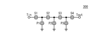
図17は、実施例3に係るフィルタ300の回路図である。図17に示すように、実施例3に係るフィルタ300は、入力端子Tinと出力端子Toutとの間に、1または複数の直列共振器S1~S4が直列に接続されている。入力端子Tinと出力端子Toutとの間に、1または複数の並列共振器P1~P3が並列に接続されている。直列共振器S1~S4および並列共振器P1~P3の少なくとも1つに実施例1、実施例1の変形例、および実施例2に係る弾性波デバイスを用いてもよい。直列共振器および並列共振器の個数等は適宜設定できる。フィルタとしてラダー型フィルタを例に示したが、フィルタは多重モード型フィルタでもよい。 Figure 17 is a circuit diagram of a filter 300 according to a third embodiment. As shown in Figure 17, in the filter 300 according to the third embodiment, one or more series resonators S1 to S4 are connected in series between the input terminal Tin and the output terminal Tout. One or more parallel resonators P1 to P3 are connected in parallel between the input terminal Tin and the output terminal Tout. The acoustic wave device according to the first embodiment, the modified example of the first embodiment, or the second embodiment may be used for at least one of the series resonators S1 to S4 and the parallel resonators P1 to P3. The number of series resonators and parallel resonators can be set as appropriate. Although a ladder-type filter is shown as an example of the filter, the filter may be a multimode filter.

なお、実施例3では、実施例1、実施例1の変形例、および実施例2に係る弾性波デバイスをフィルタに用いる場合を例に示したが、この場合に限られるわけではない。例えば、インクジェットを用いたマイクロポンプ、RF-MEMSスイッチ、または光ミラー等のアクチュエータ、もしくは、加速度、ジャイロ、またはエナジーハーベスト等のセンサに用いてもよい。 Note that in Example 3, the acoustic wave devices according to Example 1, the modified example of Example 1, and Example 2 are used as filters, but the present invention is not limited to this. For example, the acoustic wave devices may be used as actuators such as inkjet micropumps, RF-MEMS switches, or optical mirrors, or as sensors for acceleration, gyros, energy harvesting, etc.

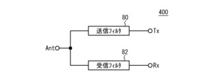
図18は、実施例4に係るデュプレクサ400の回路図である。図18に示すように、実施例4に係るデュプレクサ400は、共通端子Antと送信端子Txとの間に送信フィルタ80が接続されている。共通端子Antと受信端子Rxとの間に受信フィルタ82が接続されている。送信フィルタ80は、送信端子Txから入力された高周波信号のうち送信帯域の信号を送信信号として共通端子Antに通過させ、他の周波数の信号を抑圧する。受信フィルタ82は、共通端子Antから入力された高周波信号のうち受信帯域の信号を受信信号として受信端子Rxに通過させ、他の周波数の信号を抑圧する。送信フィルタ80および受信フィルタ82の少なくとも一方を実施例2のフィルタとしてもよい。マルチプレクサとしてデュプレクサを例に示したが、トリプレクサまたはクワッドプレクサでもよい。 18 is a circuit diagram of a duplexer 400 according to the fourth embodiment. As shown in FIG. 18, in the duplexer 400 according to the fourth embodiment, a transmission filter 80 is connected between a common terminal Ant and a transmission terminal Tx. A reception filter 82 is connected between the common terminal Ant and a reception terminal Rx. The transmission filter 80 passes a signal in a transmission band among high-frequency signals input from the transmission terminal Tx to the common terminal Ant as a transmission signal, and suppresses signals of other frequencies. The reception filter 82 passes a signal in a reception band among high-frequency signals input from the common terminal Ant to the reception terminal Rx as a reception signal, and suppresses signals of other frequencies. At least one of the transmission filter 80 and the reception filter 82 may be the filter of the second embodiment. Although a duplexer is shown as an example of a multiplexer, a triplexer or a quadplexer may also be used.

以上、本願発明の実施形態について詳述したが、本願発明はかかる特定の実施形態に限定されるものではなく、特許請求の範囲に記載された本願発明の要旨の範囲内において、種々の変形・変更が可能である。 Although the embodiment of the present invention has been described in detail above, the present invention is not limited to such a specific embodiment, and various modifications and variations are possible within the scope of the gist of the present invention as described in the claims.

10…基板、12…下部電極、14…圧電層、16…上部電極、18、18a…挿入膜、20…保護膜、22…貫通孔、30…音響反射膜、32…音響インピーダンスの低い膜、34…音響インピーダンスの高い膜、36…空隙、38…絶縁膜、40…膜、41…膜、42…膜、43、43a…膜、44…膜、50…共振領域、60…厚みすべり振動の振動方向、70…マスク層、80…送信フィルタ、82…受信フィルタ、100、110、120、200、500…弾性波デバイス、300…フィルタ、400…デュプレクサ
10...substrate, 12...lower electrode, 14...piezoelectric layer, 16...upper electrode, 18, 18a...insertion film, 20...protective film, 22...through hole, 30...acoustic reflecting film, 32...film with low acoustic impedance, 34...film with high acoustic impedance, 36...gap, 38...insulating film, 40...film, 41...film, 42...film, 43, 43a...film, 44...film, 50...resonance region, 60...vibration direction of thickness shear vibration, 70...mask layer, 80...transmitting filter, 82...receiving filter, 100, 110, 120, 200, 500...acoustic wave device, 300...filter, 400...duplexer

Claims (13)

基板と、
前記基板上に設けられた下部電極と、
前記下部電極上に設けられた上部電極と、
前記下部電極と前記上部電極の間に少なくとも一部が挟まれて前記基板上に設けられ、平面視において前記少なくとも一部を挟んで前記下部電極と前記上部電極が重なる共振領域に沿いかつ前記下部電極の一部に接する貫通孔を有する圧電層と、
前記下部電極および前記上部電極の少なくとも一方と前記圧電層との間に設けられ、前記下部電極および前記上部電極より抵抗率が高い挿入膜と、
前記上部電極の側面に前記下部電極に接続して設けられ、前記下部電極の構成元素を含む第1膜と、
前記上部電極の側面と前記第1膜の間に設けられ、前記圧電層の構成元素の濃度が前記第1膜より高い第2膜と、
前記上部電極の側面と前記第2膜の間および前記第1膜と前記第2膜の間の少なくとも一方に設けられ、前記挿入膜の構成元素であって前記圧電層の構成元素と異なる元素の濃度が前記第2膜より高くかつ前記圧電層の構成元素であって前記挿入膜の構成元素と異なる元素の濃度が前記第2膜より低い第3膜と、を備える弾性波デバイス。
A substrate;
a lower electrode provided on the substrate;
an upper electrode provided on the lower electrode;
a piezoelectric layer provided on the substrate with at least a portion thereof sandwiched between the lower electrode and the upper electrode, the piezoelectric layer having a through hole extending along a resonance region where the lower electrode and the upper electrode overlap with each other in a plan view and contacting a portion of the lower electrode;
an insertion film provided between at least one of the lower electrode and the upper electrode and the piezoelectric layer, the insertion film having a resistivity higher than that of the lower electrode and the upper electrode;
a first film provided on a side surface of the upper electrode and connected to the lower electrode, the first film including a constituent element of the lower electrode;
a second film provided between a side surface of the upper electrode and the first film, the second film having a higher concentration of a constituent element of the piezoelectric layer than that of the first film;
An elastic wave device comprising: a third film provided at least one between a side of the upper electrode and the second film and between the first film and the second film, the third film having a higher concentration of constituent elements of the insertion film that are different from the constituent elements of the piezoelectric layer than the second film and a lower concentration of constituent elements of the piezoelectric layer that are different from the constituent elements of the insertion film than the second film.
前記第2膜および前記第3膜は、前記下部電極の構成元素の濃度が前記第1膜より低い、請求項1に記載の弾性波デバイス。 The acoustic wave device of claim 1, wherein the second film and the third film have a lower concentration of the constituent elements of the lower electrode than the first film. 前記第2膜および前記第3膜は、前記下部電極の構成元素を含まない、請求項1または2に記載の弾性波デバイス。 The acoustic wave device according to claim 1 or 2, wherein the second film and the third film do not contain any constituent elements of the lower electrode. 前記第1膜は、前記挿入膜の構成元素の濃度が前記第3膜より低い、請求項1または2に記載の弾性波デバイス。 The acoustic wave device according to claim 1 or 2, wherein the first film has a lower concentration of the constituent elements of the insertion film than the third film. 前記挿入膜は無機絶縁膜である、請求項1または2に記載の弾性波デバイス。 The acoustic wave device according to claim 1 or 2, wherein the insertion film is an inorganic insulating film. 前記挿入膜は、酸化シリコン、窒化シリコン、窒化アルミニウム、酸化アルミニウム、酸化タンタル、酸化ジルコニウム、炭化シリコン、酸化イットリウム、酸化ハフニウム、酸化チタン、および酸化マグネシウムのうち少なくとも1種を含んで形成される、請求項5に記載の弾性波デバイス。 The acoustic wave device according to claim 5, wherein the insertion film is formed containing at least one of silicon oxide, silicon nitride, aluminum nitride, aluminum oxide, tantalum oxide, zirconium oxide, silicon carbide, yttrium oxide, hafnium oxide, titanium oxide, and magnesium oxide. 前記圧電層は単結晶タンタル酸リチウム層または単結晶ニオブ酸リチウム層である、請求項1または2に記載の弾性波デバイス。 The acoustic wave device according to claim 1 or 2, wherein the piezoelectric layer is a single crystal lithium tantalate layer or a single crystal lithium niobate layer. 前記下部電極および前記上部電極は前記共振領域における前記圧電層に厚みすべり振動を励振し、
前記貫通孔は前記共振領域を挟んで2つ設けられ、
前記厚みすべり振動の振動方向は2つの前記貫通孔が前記共振領域を挟んで対向する方向に交差する方向である、請求項7に記載の弾性波デバイス。
the lower electrode and the upper electrode excite thickness-shear vibration in the piezoelectric layer in the resonance region;
The through holes are provided in two positions on either side of the resonance region,
The acoustic wave device according to claim 7 , wherein a vibration direction of the thickness-shear vibration is a direction intersecting a direction in which the two through holes face each other across the resonance region.
前記貫通孔と前記共振領域における前記圧電層との間の最大の距離は、前記共振領域における前記圧電層の厚さの3.2倍以下である、請求項8に記載の弾性波デバイス。 The acoustic wave device of claim 8, wherein the maximum distance between the through hole and the piezoelectric layer in the resonance region is 3.2 times or less than the thickness of the piezoelectric layer in the resonance region. 請求項1または2に記載の弾性波デバイスを含むフィルタ。 A filter including an acoustic wave device according to claim 1 or 2. 請求項10に記載のフィルタを含むマルチプレクサ。 A multiplexer including the filter according to claim 10. 基板上に下部電極、圧電層、上部電極をこの順に形成し、かつ、前記下部電極と前記圧電層の間および前記圧電層と前記上部電極の間の少なくとも一方に前記下部電極および前記上部電極より抵抗率が高い挿入膜を形成する工程と、
前記下部電極と前記上部電極が前記圧電層を挟んで重なる共振領域の側方における前記圧電層、前記挿入膜、および前記下部電極をエッチングし、前記下部電極のエッチングにより付着した第1膜と前記上部電極の側面との間に前記圧電層のエッチングにより付着した第2膜が形成され、前記上部電極の側面と前記第2膜の間および前記第1膜と前記第2膜の間の少なくとも一方に前記挿入膜のエッチングにより付着した第3膜が形成されるようにして、前記共振領域に沿った貫通孔を前記圧電層に形成する工程と、を備える弾性波デバイスの製造方法。
forming a lower electrode, a piezoelectric layer, and an upper electrode on a substrate in this order, and forming an insertion film having a higher resistivity than the lower electrode and the upper electrode at least one between the lower electrode and the piezoelectric layer and between the piezoelectric layer and the upper electrode;
a second film attached by etching the piezoelectric layer between a first film attached by etching the lower electrode and a side of the upper electrode, and a third film attached by etching the insertion film is formed at least one of between the side of the upper electrode and the second film and between the first film and the second film, thereby forming a through hole in the piezoelectric layer along the resonance region.
前記圧電層、前記挿入膜、および前記下部電極のエッチングはイオンミリング法を用いる、請求項12に記載の弾性波デバイスの製造方法。 The method for manufacturing an acoustic wave device according to claim 12, wherein the piezoelectric layer, the insertion film, and the lower electrode are etched using an ion milling method.
JP2023148488A 2023-09-13 2023-09-13 Acoustic wave device, filter, multiplexer, and method for manufacturing an acoustic wave device Pending JP2025041295A (en)

Priority Applications (3)

Application Number Priority Date Filing Date Title
JP2023148488A JP2025041295A (en) 2023-09-13 2023-09-13 Acoustic wave device, filter, multiplexer, and method for manufacturing an acoustic wave device
US18/824,825 US20250088165A1 (en) 2023-09-13 2024-09-04 Acoustic wave device, filter, multiplexer, and method of manufacturing acoustic wave device
CN202411263508.0A CN119628592A (en) 2023-09-13 2024-09-10 Acoustic wave device, filter, multiplexer, and method for manufacturing the same

Applications Claiming Priority (1)

Application Number Priority Date Filing Date Title
JP2023148488A JP2025041295A (en) 2023-09-13 2023-09-13 Acoustic wave device, filter, multiplexer, and method for manufacturing an acoustic wave device

Publications (1)

Publication Number Publication Date
JP2025041295A true JP2025041295A (en) 2025-03-26

Family

ID=94872163

Family Applications (1)

Application Number Title Priority Date Filing Date
JP2023148488A Pending JP2025041295A (en) 2023-09-13 2023-09-13 Acoustic wave device, filter, multiplexer, and method for manufacturing an acoustic wave device

Country Status (3)

Country Link
US (1) US20250088165A1 (en)
JP (1) JP2025041295A (en)
CN (1) CN119628592A (en)

Also Published As

Publication number Publication date
US20250088165A1 (en) 2025-03-13
CN119628592A (en) 2025-03-14

Similar Documents

Publication Publication Date Title
JP7017364B2 (en) Ladder type filter, piezoelectric thin film resonator and its manufacturing method
US8084919B2 (en) Piezoelectric thin-film resonator, filter using the same, and duplexer using the same
US20070228880A1 (en) Piezoelectric thin film resonator
JP7269719B2 (en) Piezoelectric film and its manufacturing method, piezoelectric device, resonator, filter and multiplexer
JP7098453B2 (en) Elastic wave resonators, filters and multiplexers
JP7385996B2 (en) Piezoelectric thin film resonators, filters and multiplexers
US10554196B2 (en) Acoustic wave device
JP7456788B2 (en) Piezoelectric device and method for manufacturing the same
US20230172071A1 (en) Piezoelectric thin film resonator and method of manufacturing the same
JP7383417B2 (en) Acoustic wave devices and their manufacturing methods, piezoelectric thin film resonators, filters and multiplexers
JP2024140687A (en) Acoustic Wave Devices, Filters, and Multiplexers
JP7042178B2 (en) Elastic wave devices and multiplexers
US20250088165A1 (en) Acoustic wave device, filter, multiplexer, and method of manufacturing acoustic wave device
JP7027144B2 (en) Elastic wave devices and their manufacturing methods and multiplexers
JP7807927B2 (en) Thin-film piezoelectric resonators, filters and multiplexers
JP2023051766A (en) Acoustic wave device, filter, multiplexer, and method of manufacturing acoustic wave device
JP2023180558A (en) Acoustic wave devices, filters, multiplexers, and methods of manufacturing acoustic wave devices
US12413199B2 (en) Acoustic wave device, filter, multiplexer, and manufacturing method of acoustic wave device
JP2022140991A (en) Acoustic wave devices, filter and multiplexer
JP2018117194A (en) Piezoelectric thin film resonator and manufacturing method thereof, filter, and multiplexer
JP2022096249A (en) Piezoelectric element and manufacturing method thereof, filter, and multiplexer
US12255602B2 (en) Filter and multiplexer
JP2021136613A (en) Piezoelectric thin film resonator, filter, and multiplexer
JP2007288504A (en) Piezoelectric thin film resonator
US20240056052A1 (en) Acoustic wave device, filter and multiplexer