JP2024166325A - Plasma processing device and components for the mounting table - Google Patents
Plasma processing device and components for the mounting table Download PDFInfo
- Publication number
- JP2024166325A JP2024166325A JP2024157538A JP2024157538A JP2024166325A JP 2024166325 A JP2024166325 A JP 2024166325A JP 2024157538 A JP2024157538 A JP 2024157538A JP 2024157538 A JP2024157538 A JP 2024157538A JP 2024166325 A JP2024166325 A JP 2024166325A
- Authority
- JP
- Japan
- Prior art keywords
- base
- plasma processing
- electrostatic chuck
- ceramic
- mounting table
- Prior art date
- Legal status (The legal status is an assumption and is not a legal conclusion. Google has not performed a legal analysis and makes no representation as to the accuracy of the status listed.)
- Granted
Links
Images

Classifications
-
- H—ELECTRICITY
- H01—ELECTRIC ELEMENTS
- H01J—ELECTRIC DISCHARGE TUBES OR DISCHARGE LAMPS
- H01J37/00—Discharge tubes with provision for introducing objects or material to be exposed to the discharge, e.g. for the purpose of examination or processing thereof
- H01J37/32—Gas-filled discharge tubes
- H01J37/32431—Constructional details of the reactor
- H01J37/32458—Vessel
- H01J37/32477—Vessel characterised by the means for protecting vessels or internal parts, e.g. coatings
- H01J37/32495—Means for protecting the vessel against plasma
-
- H—ELECTRICITY
- H10—SEMICONDUCTOR DEVICES; ELECTRIC SOLID-STATE DEVICES NOT OTHERWISE PROVIDED FOR
- H10P—GENERIC PROCESSES OR APPARATUS FOR THE MANUFACTURE OR TREATMENT OF DEVICES COVERED BY CLASS H10
- H10P72/00—Handling or holding of wafers, substrates or devices during manufacture or treatment thereof
- H10P72/70—Handling or holding of wafers, substrates or devices during manufacture or treatment thereof for supporting or gripping
- H10P72/72—Handling or holding of wafers, substrates or devices during manufacture or treatment thereof for supporting or gripping using electrostatic chucks
- H10P72/722—Details of electrostatic chucks
-
- B—PERFORMING OPERATIONS; TRANSPORTING
- B23—MACHINE TOOLS; METAL-WORKING NOT OTHERWISE PROVIDED FOR
- B23Q—DETAILS, COMPONENTS, OR ACCESSORIES FOR MACHINE TOOLS, e.g. ARRANGEMENTS FOR COPYING OR CONTROLLING; MACHINE TOOLS IN GENERAL CHARACTERISED BY THE CONSTRUCTION OF PARTICULAR DETAILS OR COMPONENTS; COMBINATIONS OR ASSOCIATIONS OF METAL-WORKING MACHINES, NOT DIRECTED TO A PARTICULAR RESULT
- B23Q3/00—Devices holding, supporting, or positioning work or tools, of a kind normally removable from the machine
- B23Q3/15—Devices for holding work using magnetic or electric force acting directly on the work
-
- B—PERFORMING OPERATIONS; TRANSPORTING
- B28—WORKING CEMENT, CLAY, OR STONE
- B28B—SHAPING CLAY OR OTHER CERAMIC COMPOSITIONS; SHAPING SLAG; SHAPING MIXTURES CONTAINING CEMENTITIOUS MATERIAL, e.g. PLASTER
- B28B1/00—Producing shaped prefabricated articles from the material
- B28B1/001—Rapid manufacturing of 3D objects by additive depositing, agglomerating or laminating of material
-
- C—CHEMISTRY; METALLURGY
- C04—CEMENTS; CONCRETE; ARTIFICIAL STONE; CERAMICS; REFRACTORIES
- C04B—LIME, MAGNESIA; SLAG; CEMENTS; COMPOSITIONS THEREOF, e.g. MORTARS, CONCRETE OR LIKE BUILDING MATERIALS; ARTIFICIAL STONE; CERAMICS; REFRACTORIES; TREATMENT OF NATURAL STONE
- C04B37/00—Joining burned ceramic articles with other burned ceramic articles or other articles by heating
- C04B37/02—Joining burned ceramic articles with other burned ceramic articles or other articles by heating with metallic articles
- C04B37/023—Joining burned ceramic articles with other burned ceramic articles or other articles by heating with metallic articles characterised by the interlayer used
-
- H—ELECTRICITY
- H01—ELECTRIC ELEMENTS
- H01J—ELECTRIC DISCHARGE TUBES OR DISCHARGE LAMPS
- H01J37/00—Discharge tubes with provision for introducing objects or material to be exposed to the discharge, e.g. for the purpose of examination or processing thereof
- H01J37/32—Gas-filled discharge tubes
- H01J37/32009—Arrangements for generation of plasma specially adapted for examination or treatment of objects, e.g. plasma sources
- H01J37/32082—Radio frequency generated discharge
- H01J37/32091—Radio frequency generated discharge the radio frequency energy being capacitively coupled to the plasma
-
- H—ELECTRICITY
- H01—ELECTRIC ELEMENTS
- H01J—ELECTRIC DISCHARGE TUBES OR DISCHARGE LAMPS
- H01J37/00—Discharge tubes with provision for introducing objects or material to be exposed to the discharge, e.g. for the purpose of examination or processing thereof
- H01J37/32—Gas-filled discharge tubes
- H01J37/32431—Constructional details of the reactor
- H01J37/32532—Electrodes
- H01J37/32559—Protection means, e.g. coatings
-
- H—ELECTRICITY
- H01—ELECTRIC ELEMENTS
- H01J—ELECTRIC DISCHARGE TUBES OR DISCHARGE LAMPS
- H01J37/00—Discharge tubes with provision for introducing objects or material to be exposed to the discharge, e.g. for the purpose of examination or processing thereof
- H01J37/32—Gas-filled discharge tubes
- H01J37/32431—Constructional details of the reactor
- H01J37/32715—Workpiece holder
- H01J37/32724—Temperature
-
- H—ELECTRICITY
- H01—ELECTRIC ELEMENTS
- H01J—ELECTRIC DISCHARGE TUBES OR DISCHARGE LAMPS
- H01J37/00—Discharge tubes with provision for introducing objects or material to be exposed to the discharge, e.g. for the purpose of examination or processing thereof
- H01J37/32—Gas-filled discharge tubes
- H01J37/32431—Constructional details of the reactor
- H01J37/32798—Further details of plasma apparatus not provided for in groups H01J37/3244 - H01J37/32788; special provisions for cleaning or maintenance of the apparatus
- H01J37/32807—Construction (includes replacing parts of the apparatus)
-
- H—ELECTRICITY
- H02—GENERATION; CONVERSION OR DISTRIBUTION OF ELECTRIC POWER
- H02N—ELECTRIC MACHINES NOT OTHERWISE PROVIDED FOR
- H02N13/00—Clutches or holding devices using electrostatic attraction, e.g. using Johnson-Rahbek effect
-
- H—ELECTRICITY
- H05—ELECTRIC TECHNIQUES NOT OTHERWISE PROVIDED FOR
- H05H—PLASMA TECHNIQUE; PRODUCTION OF ACCELERATED ELECTRICALLY-CHARGED PARTICLES OR OF NEUTRONS; PRODUCTION OR ACCELERATION OF NEUTRAL MOLECULAR OR ATOMIC BEAMS
- H05H1/00—Generating plasma; Handling plasma
- H05H1/24—Generating plasma
- H05H1/46—Generating plasma using applied electromagnetic fields, e.g. high frequency or microwave energy
-
- H—ELECTRICITY
- H10—SEMICONDUCTOR DEVICES; ELECTRIC SOLID-STATE DEVICES NOT OTHERWISE PROVIDED FOR
- H10P—GENERIC PROCESSES OR APPARATUS FOR THE MANUFACTURE OR TREATMENT OF DEVICES COVERED BY CLASS H10
- H10P50/00—Etching of wafers, substrates or parts of devices
- H10P50/20—Dry etching; Plasma etching; Reactive-ion etching
- H10P50/24—Dry etching; Plasma etching; Reactive-ion etching of semiconductor materials
- H10P50/242—Dry etching; Plasma etching; Reactive-ion etching of semiconductor materials of Group IV materials
-
- H—ELECTRICITY
- H10—SEMICONDUCTOR DEVICES; ELECTRIC SOLID-STATE DEVICES NOT OTHERWISE PROVIDED FOR
- H10P—GENERIC PROCESSES OR APPARATUS FOR THE MANUFACTURE OR TREATMENT OF DEVICES COVERED BY CLASS H10
- H10P72/00—Handling or holding of wafers, substrates or devices during manufacture or treatment thereof
- H10P72/04—Apparatus for manufacture or treatment
- H10P72/0402—Apparatus for fluid treatment
- H10P72/0418—Apparatus for fluid treatment for etching
- H10P72/0421—Apparatus for fluid treatment for etching for drying etching
-
- H—ELECTRICITY
- H10—SEMICONDUCTOR DEVICES; ELECTRIC SOLID-STATE DEVICES NOT OTHERWISE PROVIDED FOR
- H10P—GENERIC PROCESSES OR APPARATUS FOR THE MANUFACTURE OR TREATMENT OF DEVICES COVERED BY CLASS H10
- H10P72/00—Handling or holding of wafers, substrates or devices during manufacture or treatment thereof
- H10P72/70—Handling or holding of wafers, substrates or devices during manufacture or treatment thereof for supporting or gripping
- H10P72/76—Handling or holding of wafers, substrates or devices during manufacture or treatment thereof for supporting or gripping using mechanical means, e.g. clamps or pinches
- H10P72/7604—Handling or holding of wafers, substrates or devices during manufacture or treatment thereof for supporting or gripping using mechanical means, e.g. clamps or pinches the wafers being placed on a susceptor, stage or support
- H10P72/7616—Handling or holding of wafers, substrates or devices during manufacture or treatment thereof for supporting or gripping using mechanical means, e.g. clamps or pinches the wafers being placed on a susceptor, stage or support characterised by a coating, a hardness or a material
-
- H—ELECTRICITY
- H01—ELECTRIC ELEMENTS
- H01J—ELECTRIC DISCHARGE TUBES OR DISCHARGE LAMPS
- H01J2237/00—Discharge tubes exposing object to beam, e.g. for analysis treatment, etching, imaging
- H01J2237/32—Processing objects by plasma generation
- H01J2237/33—Processing objects by plasma generation characterised by the type of processing
- H01J2237/332—Coating
-
- H—ELECTRICITY
- H01—ELECTRIC ELEMENTS
- H01J—ELECTRIC DISCHARGE TUBES OR DISCHARGE LAMPS
- H01J2237/00—Discharge tubes exposing object to beam, e.g. for analysis treatment, etching, imaging
- H01J2237/32—Processing objects by plasma generation
- H01J2237/33—Processing objects by plasma generation characterised by the type of processing
- H01J2237/334—Etching
-
- Y—GENERAL TAGGING OF NEW TECHNOLOGICAL DEVELOPMENTS; GENERAL TAGGING OF CROSS-SECTIONAL TECHNOLOGIES SPANNING OVER SEVERAL SECTIONS OF THE IPC; TECHNICAL SUBJECTS COVERED BY FORMER USPC CROSS-REFERENCE ART COLLECTIONS [XRACs] AND DIGESTS
- Y02—TECHNOLOGIES OR APPLICATIONS FOR MITIGATION OR ADAPTATION AGAINST CLIMATE CHANGE
- Y02P—CLIMATE CHANGE MITIGATION TECHNOLOGIES IN THE PRODUCTION OR PROCESSING OF GOODS
- Y02P10/00—Technologies related to metal processing
- Y02P10/25—Process efficiency
Landscapes
- Engineering & Computer Science (AREA)
- Physics & Mathematics (AREA)
- Plasma & Fusion (AREA)
- Chemical & Material Sciences (AREA)
- Analytical Chemistry (AREA)
- Ceramic Engineering (AREA)
- Mechanical Engineering (AREA)
- Electromagnetism (AREA)
- Spectroscopy & Molecular Physics (AREA)
- Manufacturing & Machinery (AREA)
- Materials Engineering (AREA)
- Structural Engineering (AREA)
- Organic Chemistry (AREA)
- Container, Conveyance, Adherence, Positioning, Of Wafer (AREA)
- Drying Of Semiconductors (AREA)
- Plasma Technology (AREA)
- Producing Shaped Articles From Materials (AREA)
- Physical Or Chemical Processes And Apparatus (AREA)
- Treatments Of Macromolecular Shaped Articles (AREA)
- Powder Metallurgy (AREA)
- Arc Welding In General (AREA)
- Chemical Vapour Deposition (AREA)
- Polymerisation Methods In General (AREA)
Abstract
Description
本開示は、載置台及びプラズマ処理装置用部品に関する。 This disclosure relates to a mounting table and a part for a plasma processing apparatus.
近年、プラズマ処理装置に設けられる部品は、高機能化を図るために構造が複雑になっており、異なる部材を接着したり、接合したりして製作される場合がある(例えば、特許文献1を参照)。 In recent years, the components installed in plasma processing devices have become more complex in structure to improve their functionality, and may be manufactured by gluing or joining different materials together (see, for example, Patent Document 1).
かかる部品の製作においては、中空構造等の複雑な構造があり、長期の生産期間及び開発期間が必要になるため、部品製作時のリードタイムの増加が課題となる。部品の製造工程における工数を減らし、リードタイムを短縮することが求められている。 The manufacturing of such parts requires long production and development periods due to their complex structures, such as hollow structures, and therefore increases in lead time during part manufacturing are an issue. There is a demand to reduce the number of steps in the parts manufacturing process and shorten the lead time.
上記課題に対して、一側面では、部品の製作時のリードタイムを短縮することを目的とする。 In one aspect, the aim of addressing the above issue is to shorten the lead time when manufacturing parts.
上記課題を解決するために、一の態様によれば、導電性材料から形成される基台と、前記基台の上面に配置され、セラミックス材料から形成される静電チャックと、前記基台と前記静電チャックとの間に設けられる境界層と、を備え、前記境界層は、前記導電性材料と前記セラミックス材料との混合物を含み、前記混合物における前記導電性材料の前記セラミックス材料に対する配合率が前記境界層において前記基台から前記静電チャックに向かって変化する、載置台が提供される。 In order to solve the above problem, according to one aspect, a mounting table is provided that includes a base formed of a conductive material, an electrostatic chuck formed of a ceramic material and disposed on the upper surface of the base, and a boundary layer provided between the base and the electrostatic chuck, the boundary layer including a mixture of the conductive material and the ceramic material, and the mixing ratio of the conductive material to the ceramic material in the mixture changes in the boundary layer from the base toward the electrostatic chuck.
一の側面によれば、部品の製作時のリードタイムを短縮することができる。 According to one aspect, the lead time for manufacturing parts can be shortened.
以下、本開示を実施するための形態について図面を参照して説明する。なお、本明細書及び図面において、実質的に同一の構成については、同一の符号を付することにより重複した説明を省く。 Below, the embodiments for carrying out the present disclosure will be described with reference to the drawings. Note that in this specification and the drawings, substantially identical configurations are designated by the same reference numerals to avoid redundant description.
[プラズマ処理装置]
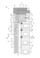
図1に示すプラズマ処理装置100は、容量結合型のプラズマ処理装置である。プラズマ処理装置100は、処理容器112及び載置台116を備えている。処理容器112は、略円筒形状を有しており、その内部空間を処理室112cとして提供している。処理容器112は、例えば、アルミニウムから構成されている。処理容器112の内部空間側の表面には、アルマイト膜、及び/又は、酸化イットリウム膜といった耐プラズマ性を有するセラミックス製の皮膜が形成されている。処理容器112は接地されている。処理容器112の側壁には、ウェハWを処理室112cに搬入し、処理室112cから搬出するための開口112pが形成されている。開口112pは、ゲートバルブGVによって開閉することが可能となっている。
[Plasma Processing Apparatus]
The
載置台116は、ウェハWを処理室112c内で支持するように構成されている。載置台116は、ウェハWを吸着する機能、ウェハWの温度を調整する機能、及び、静電チャックの基台117に高周波を伝送する構造を有している。載置台116の詳細については、後述する。
The mounting table 116 is configured to support the wafer W in the
プラズマ処理装置100は、上部電極130を有する。上部電極130は、処理容器112の上部開口内に配置されており、下部電極として機能する載置台116の略平行に配置されている。上部電極130と処理容器112との間には、絶縁性の支持部材132が介在している。
The
上部電極130は、天板134及び支持体136を有している。天板134は、略円盤状形状を有している。天板134は、導電性を有し得る。天板134は、例えば、シリコン又はアルミニウムから形成されており、その表面には、耐プラズマ性のセラミックス皮膜が形成されている。この天板134には、複数のガス吐出孔134aが形成されている。ガス吐出孔134aは、略鉛直方向に延びている。
The
支持体136は、天板134を着脱自在に支持している。支持体136は、例えば、アルミニウムから形成されている。支持体136には、ガス拡散室136aが形成されている。ガス拡散室136aからは、複数のガス吐出孔134aにそれぞれ連通する複数の孔136bが延びている。ガス拡散室136aには、ポート136cを介して配管138が接続している。配管138には、ガス供給部139が接続されている。
The
プラズマ処理装置100は、排気装置150を有する。排気装置150は、ターボ分子ポンプ、ドライポンプといった一以上のポンプ、及び、圧力調整弁を含んでいる。排気装置150は、処理容器112に形成された排気口に接続されている。
The
プラズマ処理装置100は、第1制御部151を有する。第1制御部151の記憶部には、プラズマ処理装置100で実行される各種処理をプロセッサにより制御するための制御プログラム及びレシピデータが格納されている。例えば、第1制御部151の記憶部には、エッチング処理等のプラズマ処理をプラズマ処理装置100で実行するための制御プログラム及びレシピデータが記憶されている。
The
以下、図1に加えて、図2を参照し、載置台116及び載置台116に付随するプラズマ処理装置100の構成要素について詳細に説明する。図2は、図1に示すプラズマ処理装置100の載置台116の一部を拡大して示す断面図である。
Below, the mounting table 116 and the components of the
載置台116は、基台117及び静電チャック120を有している。基台117は、たとえばアルミニウム合金(Al)、チタン(Ti)、シリコンカーバイト(SiC)等から形成されている。基台117は、処理容器112の底部から上方に延びる支持部材114によって支持されている。支持部材114は、絶縁性の部材であり、例えば、酸化アルミニウム(アルミナ)から形成されている。また、支持部材114は、略円筒形状を有している。
The mounting table 116 has a
基台117は、導電性を有する金属、例えば、アルミニウムから形成されている。基台117は、略円盤形状を有している。基台117は、中央部117a及び周縁部117bを有している。中央部117aは、略円盤形状を有している。中央部117aは、基台117の第1上面117cを提供している。第1上面117cは、略円形の面である。
The
周縁部117bは、中央部117aに連続しており、径方向(鉛直方向に延びる軸線Zに対して放射方向)において中央部117aの外側で、周方向(軸線Zに対して周方向)に延在している。一実施形態では、周縁部117bは、中央部117aと共に、基台117の下面117dを提供している。また、周縁部117bは、第2上面117eを提供している。第2上面117eは、帯状の面であり、径方向において第1上面117cの外側にあり、且つ、周方向に延びている。また、第2上面117eは、鉛直方向において、第1上面117cよりも下面117dの近くにある。
The
基台117には、給電体119が接続されている。給電体119は、例えば給電棒であり、基台117の下面117dに接続されている。給電体119は、アルミニウム又はアルミニウム合金から形成されている。給電体119には、第1の高周波電源62が整合器66を介して接続されている。また、給電体119には、第2の高周波電源64が整合器68を介して接続されている。
A
基台117には、冷媒用の流路117fが形成されている。流路117fは、基台117内において、例えば渦巻状に延在している。この流路117fには、チラーユニットから冷媒が供給される。流路117fに供給される冷媒は、一実施形態では、その気化によって吸熱し、冷却を行う冷媒である。この冷媒は、例えば、ハイドロフルオロカーボン系の冷媒であり得る。
A
静電チャック120は、吸着部123を有している。吸着部123は、基台117上の基台121の上に設けられている。基台121は、下部電極を構成しており、基台117の上に設けられている。基台121は、導電性を有している。基台121は、例えば、窒化アルミニウム又は炭化ケイ素に導電性を付与したセラミックス製であってもよく、或いは、金属(例えば、チタン)製であってもよい。
The
基台121は、略円盤形状を有している。基台121は、中央部121a及び周縁部121bを有している。中央部121aは、略円盤形状を有している。中央部121aは、基台121の第1上面121cを提供している。第1上面121cは、略円形の面である。
The
周縁部121bは、中央部121aに連続しており、径方向において中央部121aの外側で、周方向に延在している。一実施形態では、周縁部121bは、中央部121aと共に、基台121の下面121dを提供している。また、周縁部121bは、第2上面121eを提供している。この第2上面121eは、帯状の面であり、径方向において第1上面121cの外側で周方向に延びている。また、第2上面121eは、鉛直方向において、第1上面121cよりも下面121dの近くにある。
The
吸着部123と基台121との間には境界層129が形成されている。吸着部123は、略円盤形状を有しており、セラミックスから形成されている。吸着部123を構成するセラミックスは、室温(例えば、20度)以上、400℃以下の温度範囲において、1×10¹⁵Ω・cm以上の体積抵抗率を有するセラミックスであり得る。このようなセラミックスとして、例えば、酸化アルミニウム(アルミナ)が用いられ得る。
A
静電チャック120は、軸線Z、即ち静電チャック120の中心軸線に対して同心の複数の領域RNを含んでいる。一実施形態では、静電チャック120は、第1領域R1、第2領域R2、及び、第3領域R3を含んでいる。第1領域R1は、軸線Zに交差しており、第3領域R3は、静電チャック120のエッジを含む領域であり、第2領域R2は、第1領域R1と第3領域R3との間にある。一例では、第1領域R1は、静電チャック120の中心から半径120mmまでの領域であり、第2領域R2は、静電チャック120において半径120mmから半径135mmまでの領域であり、第3領域R3は、静電チャック120において半径135mmから半径150mmまでの領域である。なお、静電チャック120の領域の個数は、一以上の任意の個数であり得る。
The
静電チャック120の吸着部123は、電極膜125を内蔵している。電極膜125には、直流電源が電気的に接続されている。直流電源からの直流電圧が電極膜125に与えられると、吸着部123はクーロン力といった静電力を発生し、当該静電力によってウェハWを保持する。
The
吸着部123は、複数のヒータHNを更に内蔵している。複数のヒータHNは、静電チャックの上記複数の領域RN内にそれぞれ設けられている。一実施形態では、複数のヒータHNは、第1のヒータ156、第2のヒータ157、及び、第3のヒータ158を含んでいる。第1のヒータ156は第1領域R1内に設けられており、第2のヒータ157は第2領域R2内に設けられており、第3のヒータ158は第3領域R3内に設けられている。複数のヒータHNは、ヒータ電源に接続されている。
The
基台121と基台117の間には、複数の第1の弾性部材EM1が設けられている。複数の第1の弾性部材EM1は、静電チャック120を基台117から上方に離間させている。複数の第1の弾性部材EM1の各々は、Oリングである。複数の第1の弾性部材EM1は、互いに異なる直径を有しており、軸線Zに対して同心状に設けられている。また、複数の第1の弾性部材EM1は、静電チャック120の隣接する領域の境界及び静電チャック120のエッジの下方に設けられている。一実施形態では、複数の第1の弾性部材EM1は、弾性部材165、弾性部材167、及び、弾性部材169を含んでいる。弾性部材165は、第1領域R1と第2領域R2の境界の下方に設けられており、弾性部材167は、第2領域R2と第3領域R3の境界の下方に設けられており、弾性部材169は、静電チャック120のエッジの下方に設けられている。
A plurality of first elastic members EM1 are provided between the base 121 and the
複数の第1の弾性部材EM1は、基台117の第1上面117cによって提供される溝の中に部分的に配置されており、第1上面117cと基台121の下面121dに接している。複数の第1の弾性部材EM1は、基台117と基台121と共に、基台117の第1上面117cと基台121の下面121dとの間に、複数の伝熱空間DSNを画成している。複数の伝熱空間DSNは、静電チャック120の複数の領域RNそれぞれの下方において延在しており、互いに分離されている。一実施形態では、複数の伝熱空間DSNは、第1の伝熱空間DS1、第2の伝熱空間DS2、及び、第3の伝熱空間DS3を含んでいる。第1の伝熱空間DS1は、弾性部材165の内側にあり、第2の伝熱空間DS2は、弾性部材165と弾性部材167との間にあり、第3の伝熱空間DS3は、弾性部材167と弾性部材169との間にある。後述するように、複数の伝熱空間DSNには、伝熱ガス(例えば、Heガス)が供給される。なお、複数の伝熱空間DSNの各々の鉛直方向における長さは、例えば、0.1mm以上2.0mm以下の長さに設定される。
The plurality of first elastic members EM1 are partially disposed in grooves provided by the first
複数の第1の弾性部材EM1は、Heガスが供給されている複数の伝熱空間DSNの各々の熱抵抗よりも高い熱抵抗を有するように構成される。複数の伝熱空間DSNの熱抵抗は、伝熱ガスの熱伝導率、その鉛直方向の長さ、及びその面積に依存する。また、複数の第1の弾性部材EM1の各々の熱抵抗は、その熱伝導率、その鉛直方向における厚さ、及び、その面積に依存する。したがって、複数の第1の弾性部材EM1の各々の材料、厚さ、及び、面積は、複数の伝熱空間DSNの各々の熱抵抗に応じて、決定される。なお、複数の第1の弾性部材EM1には、低い熱伝導率及び高い耐熱性が要求され得る。したがって、複数の第1の弾性部材EM1は、例えば、パーフロロエラストマーから形成され得る。 The multiple first elastic members EM1 are configured to have a thermal resistance higher than the thermal resistance of each of the multiple heat transfer spaces DSN to which He gas is supplied. The thermal resistance of the multiple heat transfer spaces DSN depends on the thermal conductivity of the heat transfer gas, its vertical length, and its area. In addition, the thermal resistance of each of the multiple first elastic members EM1 depends on its thermal conductivity, its vertical thickness, and its area. Therefore, the material, thickness, and area of each of the multiple first elastic members EM1 are determined according to the thermal resistance of each of the multiple heat transfer spaces DSN. Note that the multiple first elastic members EM1 may be required to have low thermal conductivity and high heat resistance. Therefore, the multiple first elastic members EM1 may be formed, for example, from a perfluoroelastomer.
載置台116は、締付部材171を有する。締付部材171は、金属から形成されており、基台121及び複数の第1の弾性部材EM1を、当該締付部材171と基台117との間に挟持するように構成されている。締付部材171は、基台121と基台117との間の当該締付部材171を介した熱伝導を抑制するために、低い熱伝導率を有する材料、例えば、チタンから形成される。
The mounting table 116 has a
一実施形態において、締付部材171は、筒状部171a及び環状部171bを有している。筒状部171aは、略円筒形状を有しており、その下端において第1下面171cを提供している。第1下面171cは、周方向に延びる帯状の面である。
In one embodiment, the
環状部171bは、略環状板形状を有しており、筒状部171aの上側部分の内縁に連続して、当該筒状部171aから径方向内側に延びている。この環状部171bは、第2下面171dを提供している。第2下面171dは、周方向に延びる帯状の面である。
The
締付部材171は、第1下面171cが基台117の第2上面117eに接し、第2下面171dが基台121の第2上面121eに接するように配置される。また、締付部材171は、基台117の周縁部117bに対してねじ173によって固定される。このねじ173の締付部材171に対する螺合を調整することにより、複数の第1の弾性部材EM1の潰し量が調整される。これにより、複数の伝熱空間DSNの鉛直方向における長さが調整される。
The
一実施形態では、締付部材171の環状部171bの内縁部下面と基台121の第2上面121eとの間には、第2の弾性部材175が設けられている。第2の弾性部材175は、Oリングであり、締付部材171の第2下面171dと基台121の第2上面121eとの摩擦により生じ得るパーティクル(例えば、金属粉)が、吸着部123側に移動することを抑制する。
In one embodiment, a second
また、第2の弾性部材175は、複数の第1の弾性部材EM1が発生する反力よりも小さい反力を発生する。換言すると、複数の第1の弾性部材EM1は、当該複数の第1の弾性部材EM1が発生する反力が第2の弾性部材175が発生する反力よりも大きくなるように構成される。さらに、この第2の弾性部材175は、高い耐熱性を有し、且つ、低い熱伝導率を有する材料として、パーフロロエラストマーから形成され得る。
The second
締付部材171の上には、ヒータ176が設けられている。このヒータ176は、周方向に延在しており、フィルタを介してヒータ電源に接続されている。フィルタは、高周波がヒータ電源に侵入することを防止するために、設けられている。
A
ヒータ176は、第1の膜180と第2の膜182の間に設けられている。第1の膜180は、第2の膜182に対して締付部材171側に設けられている。第1の膜180は、第2の膜182の熱伝導率よりも低い熱伝導率を有している。例えば、第1の膜180は、ジルコニア製の溶射膜であり、第2の膜182は酸化イットリウム(イットリア)製の溶射膜であり得る。また、ヒータ176は、タングステンの溶射膜であり得る。
The
第2の膜182上には、エッジリングFRが設けられている。エッジリングFRは、例えばSiから形成されている。エッジリングFRは、ヒータ176からの熱によって加熱される。また、ヒータ176からの熱流束の多くは、第1の膜180よりも第2の膜182に向かい、当該第2の膜182を介してエッジリングFRに向かう。したがって、エッジリングFRが効率的に加熱される。
An edge ring FR is provided on the
また、載置台116の基台117、締付部材171等は、それらの外周側において一以上の絶縁性部材186によって覆われている。一以上の絶縁性部材186は、例えば、酸化アルミニウム又は石英から形成されている。
In addition, the
以上説明したように、載置台116では、複数の第1の弾性部材EM1によって基台117と基台121とが互いに離間されている。また、この載置台116では、基台121と吸着部123との接合に、接着剤が用いられていない。したがって、静電チャック120の温度を、高温に設定することが可能である。また、複数の伝熱空間DSNに供給される伝熱ガスを介して静電チャック120と基台117との間の熱交換がなされ得るので、静電チャック120の温度を低温に設定することも可能である。また、この載置台116では、給電体119、基台117、及び、締付部材171により、静電チャック120の基台121に対する高周波の給電ルートが確保されている。さらに、給電体119が、静電チャック120の基台121に直接接続されるのではなく、基台117に接続されるので、当該給電体119の構成材料としてアルミニウム又はアルミニウム合金を採用することができる。したがって、13.56MHz以上の高い周波数の高周波が用いられる場合であっても、給電体119における高周波の損失が抑制される。
As described above, in the mounting table 116, the
また、上述したように、一実施形態では、締付部材171の環状部171bの内縁部下面と基台121の第2上面121eとの間には、第2の弾性部材175が設けられている。基台121の周縁部121bの第2上面121eと締付部材171の第2下面171dは、互いに接しているので、それらの接触箇所において摩擦が生じ、パーティクル(例えば、金属粉)が発生することがある。第2の弾性部材175は、このようなパーティクルが発生しても、吸着部123及び当該吸着部123上に載置されるウェハWに、パーティクルが付着することを抑制し得る。
As described above, in one embodiment, a second
また、複数の第1の弾性部材EM1は、これら複数の第1の弾性部材EM1が発生する反力が第2の弾性部材175が発生する反力よりも大きくなるように構成される。これにより、静電チャック120を基台117から確実に離間させることができる。
The multiple first elastic members EM1 are configured so that the reaction force generated by the multiple first elastic members EM1 is greater than the reaction force generated by the second
また、一実施形態では、複数の第1の弾性部材EM1は、複数の伝熱空間DSNにHeガスが供給されているときの当該複数の伝熱空間DSNの熱抵抗よりも高い熱抵抗を有するように構成される。また、複数の第1の弾性部材EM1は、例えば、パーフロロエラストマーから形成される。これら複数の第1の弾性部材EM1によれば、静電チャック120と基台117との間では、複数の第1の弾性部材EM1を介した熱伝導よりも複数の伝熱空間DSNを介した熱伝導が優位となる。したがって、静電チャック120の温度分布が均一化され得る。
In one embodiment, the multiple first elastic members EM1 are configured to have a thermal resistance higher than the thermal resistance of the multiple heat transfer spaces DSN when He gas is supplied to the multiple heat transfer spaces DSN. The multiple first elastic members EM1 are formed, for example, from a perfluoro elastomer. With these multiple first elastic members EM1, between the
また、一実施形態では、ウェハWと吸着部123との間に供給される伝熱ガス用のガスライン190が接着剤を用いずに形成されている。また、このガスライン190を部分的に構成するスリーブ192が配置される収容空間を画成する基台121の面121fが皮膜194で覆われており、且つ、当該収容空間を封止するように皮膜194と基台117との間において絶縁性の第3の弾性部材196が設けられている。これにより、プラズマが基台121と基台117との間に侵入すること、及び、それに伴う基台121の絶縁破壊が抑制される。
In one embodiment, the gas line 190 for the heat transfer gas supplied between the wafer W and the
また、上述した載置台116を有するプラズマ処理装置100によれば、低い温度から高い温度までの広い温度帯において、ウェハWに対するプラズマ処理を行うことができる。
In addition, the
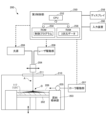
[3Dプリンタの構成]
次に、3Dプリンタ200の構成一例について、図3を参照しながら説明する。図3は、一実施形態に係る3Dプリンタ200の構成の一例を示す。本実施形態に係る3Dプリンタ200は、プラズマ処理装置内で使用される部品を形成(製造)する装置の一例である。ただし、部品を形成する装置は、図3に示す3Dプリンタ200の構成に限られない。
[3D Printer Configuration]
Next, an example of the configuration of the
また、本実施形態では、3Dプリンタ200にて形成する部品の一例として、構造が複雑な下部電極として機能する載置台116を挙げて説明する。しかし、3Dプリンタ200にて形成する部品はこれに限られず、例えば、上部電極130であってもよい。例えば、異種材料を含む部品や接着できない異種材料をねじ止めして固定している部品であってもよい。その他、プラズマ処理装置100に配置される部品であればいずれの部品であってもよい。
In addition, in this embodiment, the mounting table 116, which functions as a lower electrode with a complex structure, is described as an example of a part formed by the
3Dプリンタ200は、チャンバ210にて3次元形状の造形物を形成することが可能である。本実施形態にかかる3Dプリンタ200では、3次元形状の造形物として載置台116を形成するための3次元データをRAM256等の記憶部に記憶し、3次元データに基づき載置台116を製造する。載置台116は、テーブルに備えられたステージ202の載置面上で形成される。ステージ202は、載置台116の形成の進行に応じて、例えば除々に下降させるように昇降可能である。
The
本実施形態では、テーブルに備えられた原料格納部203に載置台116を形成する原料の粉末が格納されている。原料は、載置台116を構成する各部材の材料と同じであればよい。例えば、載置台116を構成する部材のうち、基台117、121がアルミニウム合金により形成され、静電チャック120がSiCにより形成される場合、原料格納部203にはアルミニウム合金の粉末とSiCの粉末とが分けて格納される。
In this embodiment, the raw material powder that forms the mounting table 116 is stored in the raw
ただし、基台117、121の材料はアルミニウム合金に限られず、SiC等のセラミックスであってもよい。また、静電チャック120の材料はSiCに限られず、アルミナ等のセラミックスであってもよい。基台117、121がSiCにより形成され、静電チャック120がアルミナにより形成される場合、原料格納部203にはSiCの粉末とアルミナの粉末とが分けて格納される。なお、基台117、基台121、静電チャック120とを構成する各材料の原料は粉末状に限られず、ワイヤ状であってもよい。また、本実施形態では、基台117と静電チャック120とは異種材料にて形成される。
However, the material of the
チャンバ210内では、原料の粉末を供給しながらエネルギービームを照射し、原料の粉末を溶かす。本実施形態では、照射するエネルギービームとしてレーザ光A(光学レーザ)が用いられる。
In the
レーザ光Aは、光源206から出力され、2次元走査するレーザ走査装置204により位置決めされた所定の位置に照射される。光源206及びレーザ走査装置204は、チャンバ210の外部に配置されることが好ましい。レーザ走査装置204は、第2制御部250がレーザ駆動部208を駆動することにより所定の位置に移動する。
Laser light A is output from the
レーザ走査装置204は、ステージ202上でレーザ光Aを少なくとも2次元(XY)方向に走査する。例えばレーザ走査装置204は、載置台116の立体構造を示す3次元データに応じてステージ202上でレーザ光Aの照射スポットを移動させるよう制御される。具体的には、第2制御部250の制御により、レーザ走査装置204は載置台116を構成する基台117、121及び静電チャック120等のパーツの形成の進行に応じて2次元(XY)方向に走査する。
The
第2制御部250は、ローラ駆動部207を制御し、ローラ205を駆動させる。これにより、基台117の材料であるアルミニウム合金の粉末及び/又は静電チャック120の材料であるSiCの粉末は、レーザ光走査スペース209に供給される。
The
なお、原料格納部203は、加熱手段により温度が調整されていることが好ましい。また、チャンバ210には、不活性ガスの供給及びチャンバ210内の排気が可能な機構が設けられていることが好ましい。
It is preferable that the temperature of the raw
レーザ走査装置204が2次元方向に走査するレーザ光Aは、チャンバ210の天井部、例えばステージ202の中心の直上に設けられたレーザ透過窓211を介してステージ202上の照射領域に照射される。レーザ光Aは、ステージ202上のアルミニウム合金の粉末及び/又はSiCの粉末を加熱し(図3のB参照)、粉末を融解固化させ、載置台116を形成する。このようにして、基台117、静電チャック120が順に立体的に形成され、載置台116の製造が完成する。
The laser beam A scanned in two dimensions by the
第2制御部250は、CPU252、ROM254及びRAM256を有する。第2制御部250は、原料格納部203からの原料粉末の供給制御、ステージ202の昇降制御を行う。また、第2制御部250は、光源206の点灯制御、レーザ走査装置204の走査制御、ローラ駆動部207及びレーザ駆動部208の制御を行う。これにより、第2制御部250は、載置台116を製造する動作を制御する。
The
CPU252が実行する制御プログラムは、例えばROM254に格納されている。CPU252は、例えばRAM256に格納された3次元データに基づき、制御プログラムを実行することで、載置台116の製造を制御する。なお、制御プログラムは、固定的な記録媒体に格納してもよいし、各種フラッシュメモリや光(磁気)ディスク等の着脱可能であって、コンピュータ読み取り可能な記録媒体に格納してもよい。
The control program executed by the
さらに、第2制御部250は、ディスプレイ258及びキーボードやポインティングデバイスなどの入力装置260を有する。ディスプレイ258は、エッジリング87の修復進行状態等を表示するために用いられる。入力装置260は、エッジリング87の修復動作の開始、停止などの指令や設定時の制御パラメータの入力などに用いられる。
The
3次元データは、載置台116を製造するためのデータであり、RAM256等の記憶部に記憶される。3次元データには、基台117の立体構造と基台117内の流路117f等の中空構造、基台121及び静電チャック120等、載置台116を構成する各種部分に関するデータが含まれる。また、3次元データには、静電チャック120の立体構造と、静電チャック120に埋設されるヒータHN及び電極膜125に関するデータが含まれる。また、3次元データには、基台117、121と静電チャック120の間に形成される境界層に関するデータが含まれる。
The three-dimensional data is data for manufacturing the mounting table 116, and is stored in a storage unit such as the
[3Dプリンタの動作]
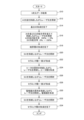
次に、3Dプリンタ200の動作の一例について、図4及び図5を参照しながら説明する。図4は、一実施形態に係る部品の形成処理の一例を示すフローチャートである。図5は、一実施形態に係る部品の形成方法を説明するための図である。
[Operation of 3D printer]
Next, an example of the operation of the
本処理が開始されると、第2制御部250は、RAM256に格納された3次元データを取得する(ステップS10)。第2制御部250は、3次元データに基づき、アルミニウム合金の粉末をレーザ光走査スペース209に供給しながら該粉末にレーザ光を照射する(ステップS12)。その際、第2制御部250は、ローラ駆動部207を制御してローラ205を動作させ、アルミニウム合金の粉末をレーザ光走査スペース209に供給する。また、第2制御部250は、レーザ駆動部208を制御してレーザ走査装置204を所定の位置に移動させ、レーザ光をアルミニウム合金の粉末に照射する。第2制御部250は、ローラ205を用いてアルミニウム合金の粉末を供給し、レーザ光により融解固化させる前記の動作を繰り返し実行する。これにより、第2制御部250は、基台117、121の形成を完了させる(ステップS14)。
When this process is started, the
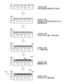
図5(1)に基台117、121の形成工程の一部を示す。この工程は、金属の原料の一例であるアルミニウム合金の粉末を供給しながらその粉末にレーザ光を照射することで基台を形成する第1の工程の一例である。これによれば、3次元データに基づき基台117の内部の流路117fの中空構造についても精密に形成することができる。
Figure 5 (1) shows part of the process for forming the
図4に戻り、次に、第2制御部250は、アルミニウム合金の粉末とSiCの粉末との配合率を変えてレーザ光走査スペース209に供給しながら該粉末にレーザ光を照射する(ステップS16)。その際、第2制御部250は、3次元データに基づきアルミニウム合金の粉末の配合率を100%から徐々に減らし、0%まで連続的に変えて供給する。また、第2制御部250は、3次元データに基づきSiCの粉末の配合率を0%から徐々に増やし、100%まで連続的に変えて供給する。
Returning to FIG. 4, the
これにより、レーザ光走査スペース209に供給されるアルミニウム合金の粉末とSiCの粉末との配合率が、アルミニウム合金が多い状態からSiCが多い状態へと変化する。第2制御部250は、ローラ205を用いて所定の比率に配合されたアルミニウム合金の粉末とSiCの粉末とをレーザ光走査スペース209に供給し、レーザ光をアルミニウム合金の粉末とSiCの粉末とに照射し、融解固化させる動作を繰り返し実行する。これにより、第2制御部250は、境界層129の形成を完了させる(ステップS18)。
As a result, the mixture ratio of aluminum alloy powder and SiC powder supplied to the laser
図5(2)に境界層129の形成工程の一例を示す。この工程は、基台121上に金属の原料の一例であるアルミニウム合金の粉末とセラミックスの原料の一例であるSiCの粉末とが所定の割合で配合された粉末を供給しながらその粉末にレーザ光を照射することで基台上に境界層を形成する第2の工程の一例である。
Figure 5 (2) shows an example of the process for forming the
図4に戻り、次に、第2制御部250は、SiCの粉末をレーザ光走査スペース209に供給しながら該粉末にレーザ光を照射する(ステップS20)。第2制御部250は、ローラ205を用いてSiCの粉末を供給し、レーザ光により融解固化させる前記の動作を繰り返し実行する。これにより、静電チャック120の吸着部123を形成するセラミックス層がヒータ層の下まで形成される(ステップS22)。
Returning to FIG. 4, the
図5(3)にセラミックス層の形成工程の一例を示す。この工程は、セラミックスの原料の一例であるSiCの粉末を供給しながらその粉末にレーザ光を照射することで境界層129の上にセラミックス層(吸着部123)を形成する第3の工程の一例である。
Figure 5 (3) shows an example of the ceramic layer formation process. This process is an example of the third process in which a ceramic layer (adsorption portion 123) is formed on the
図4に戻り、次に、第2制御部250は、ヒータの原料の粉末をレーザ光走査スペース209に供給しながら該粉末にレーザ光を照射する(ステップS24)。第2制御部250は、ローラ205を用いてヒータHNの原料の粉末を供給し、レーザ光により融解固化させる動作を行い、吸着部123内にヒータ層を形成する。
Returning to FIG. 4, the
図5(4)にヒータHNの形成工程の一例を示す。この工程は、ヒータHNの原料の粉末を供給しながらヒータHNの原料にエネルギービームを照射することでヒータHNを形成する第4の工程の一例である。 Figure 5 (4) shows an example of a process for forming the heater HN. This process is an example of the fourth process in which the heater HN is formed by irradiating the heater HN raw material with an energy beam while supplying the heater HN raw material powder.
図4に戻り、次に、第2制御部250は、SiCの粉末をレーザ光走査スペース209に供給しながら該粉末にレーザ光を照射する(ステップS26)。第2制御部250は、ローラ205を用いてSiCの粉末を供給し、レーザ光により融解固化させる前記の動作を繰り返し実行する。これにより、吸着部123を形成するセラミックス層が電極膜の下まで形成される(ステップS28)。
Returning to FIG. 4, the
次に、第2制御部250は、電極膜の原料の粉末をレーザ光走査スペース209に供給しながら該粉末にレーザ光を照射する(ステップS30)。第2制御部250は、ローラ205を用いて電極膜の原料の粉末を供給し、レーザ光により融解固化させる動作を行い、静電チャック120内に電極層を形成する。
Next, the
図5(5)に電極層(電極膜125)の形成工程の一例を示す。この工程は、電極膜125の原料の粉末を供給しながら電極膜125の原料にレーザ光を照射することで電極膜125を形成する第5の工程の一例である。
Figure 5 (5) shows an example of a process for forming an electrode layer (electrode film 125). This process is an example of a fifth process in which the
図4に戻り、次に、第2制御部250は、SiCの粉末をレーザ光走査スペース209に供給しながら該粉末にレーザ光を照射する(ステップS32)。第2制御部250は、ローラ205を用いてSiCの粉末を供給し、レーザ光により融解固化させる動作を繰り返し実行する。これにより、吸着部123の残りのセラミックス層が形成され(ステップS34)、本処理を終了する。これにより、図5(6)に示す静電チャック120の吸着部123の形成が完了し、載置台116の製造が終了する。
Returning to FIG. 4, the
かかる部品の形成方法によれば、基台121と吸着部123との間に各部材の材料の配合率を変えて形成した境界層129が設けられる。その際、異種材料の境界層129を滑らかに、かつグラディエーション状に形成することで載置台116の接着層を不要とすることができる。これにより、載置台116の異種材料間における熱伝達率を向上させ、熱特性を改善できる。
According to this method of forming parts, a
境界層129の各材料の配合率は、基台121に近いほど基台121の材料であるアルミニウム合金の配合率が吸着部123の材料であるSiCの配合率よりも高くなる。逆に、吸着部123に近いほど吸着部123の材料であるSiCの配合率が基台121の材料であるアルミニウム合金の配合率よりも高くなる。
The mixture ratio of each material in the
このように境界層129は、アルミニウム合金とSiCの配合率がグラディエーション状に変化した材料を溶融固化し、積層することで形成される。境界層129の形成において異種材料の配合率がグラディエーション状に変化して積層されることを「傾斜積層」ともいう。
In this way, the
かかる境界層129の形成工程では、基台121と吸着部123の間の境界層129を傾斜積層させることで、載置台116の異種材料間における熱伝達率を傾斜積層されていない場合と比べてより向上させることができる。また、かかる境界層129の形成工程では、基台121と吸着部123とを接着する接着層をなくすことで製造の工数を減らすことができ、製造のリードタイムを短縮できる。
In the process of forming such a
さらに、流路構造や配線構造等を3次元的に配置することで載置台116の高機能化を図ることができる。 Furthermore, by arranging the flow path structure, wiring structure, etc. three-dimensionally, the functionality of the mounting table 116 can be improved.
なお、3Dプリンタ200では、第1の工程→第2の工程→第3の工程の順に各工程を実行してもよいし、第3の工程→第2の工程→第1の工程の順に各工程を実行してもよい。これにより、下部電極として機能する載置台2と同様に、上部電極として機能する上部電極130を3Dプリンタ200により製造することができる。
The
[境界層129のバリエーション]
境界層129は、アルミニウム合金の粉末とSiCの粉末との配合率を線形的に変化させるスロープ状(グラディエーション状)の傾斜積層に限られない。境界層129は、アルミニウム合金の粉末とSiCの粉末との配合率を段階的に変化させるステップ状の傾斜積層であってもよい。また、基台121及び吸着部123の材料毎の線膨張係数に応じて境界層129の傾斜(各材料の配合率)を変えてもよい。
[Variations of Boundary Layer 129]
The
[3Dプリンタの種類]
なお、本実施形態では、載置台116の製造を行う3Dプリンタ200の一例として粉末床溶融型の3Dプリンタを適用した。粉末床溶融型の3Dプリンタでは、ステージ202に粉末状の原料を敷き詰めてレーザ光等で溶かし、再び粉末状の原料を敷き詰めてレーザ光等で溶かす作業を繰り返して部品を形成する。このため、粉末床溶融型の3Dプリンタは、予め形成する立体構造が明確であり、かつ中空構造等の複雑な構造を有する載置台116及び上部電極130の構造物の製造に適している。
[3D printer types]
In this embodiment, a powder bed fusion type 3D printer is used as an example of the
しかし、3Dプリンタ200は、かかる構成の3Dプリンタに限られず、例えば指向性エネルギー型の3Dプリンタであってもよいし、それ以外の方法を用いる3Dプリンタであってもよい。前記以外の方法を用いる3Dプリンタとしては、結合剤噴射型の3Dプリンタ、シート積層型の3Dプリンタ、光重合硬化(光造形)形の3Dプリンタ、材料押出し(熱溶融積層)形の3Dプリンタが一例として挙げられる。
However, the
また、製造対象の部品の材料が樹脂材料又はセラミックスの場合、3Dプリンタが行う樹脂材料の原料を供給しながらエネルギービームを照射する工程では、エネルギービームとして紫外線が使用される。これにより、本実施形態に係る部品の形成方法によれば、金属材料の部品だけでなく、樹脂やセラミックス材料の部品を形成することができる。部品の材料が樹脂又はセラミックス材料の場合の3Dプリンタとしては、インクジェットヘッドから噴射した樹脂を紫外線で固めて積層する材料噴射型の3Dプリンタが一例として挙げられる。 In addition, when the material of the parts to be manufactured is a resin material or ceramics, ultraviolet light is used as the energy beam in the process performed by the 3D printer in which the raw material of the resin material is supplied while the energy beam is being irradiated. As a result, the part formation method according to this embodiment can form not only parts made of metal materials, but also parts made of resin or ceramic materials. One example of a 3D printer for parts made of resin or ceramic materials is a material-jetting 3D printer that solidifies and layers resin sprayed from an inkjet head with ultraviolet light.
[異種のセラミックスの積層構造]
最後に、3Dプリンタを用いた異種のセラミックスの積層構造を有する部品の製造について簡単に説明する。例えば、基台121の材料がSiCであり、吸着部123の材料がアルミナである場合、載置台116は、異種のセラミックスの積層構造を有する部品の一例となる。この場合、基台121の材料は第1のセラミックスの原料の一例であり、吸着部123の材料は第1のセラミックスとは異なる第2のセラミックスの原料の一例である。
[Laminated structure of different ceramics]
Finally, a brief description will be given of the manufacture of a part having a laminated structure of different ceramics using a 3D printer. For example, when the material of the
このように異種のセラミックスの積層構造を有する部品を3Dプリンタ200を用いて形成する方法では、まず、第1のセラミックスと第2のセラミックスの一方の原料を供給しながら、その原料にエネルギービームを照射する工程を実行する。例えば、図3の第2制御部250は、3次元データに基づき、SiCの粉末をレーザ光走査スペース209に供給しながらSiCの粉末に紫外線を照射する。本工程及び以下の工程において照射されるエネルギービームは、紫外線に限られず、その他の周波数帯域の光であってもよい。
In this method of forming a part having a laminated structure of different ceramics using the
次に、第1のセラミックスの原料と第2のセラミックスの原料とを供給しながら、その原料にエネルギービームを照射する工程を実行する。例えば、第2制御部250は、3次元データに基づき、SiCの粉末とアルミナの粉末とをレーザ光走査スペース209に供給しながらSiCの粉末とアルミナの粉末に紫外線を照射する。
Next, a process is carried out in which the raw materials for the first ceramic and the raw materials for the second ceramic are supplied while irradiating the raw materials with an energy beam. For example, the
最後に、第1のセラミックスと第2のセラミックスとの他方の原料を供給しながら、その原料にエネルギービームを照射する工程を実行する。例えば、第2制御部250は、3次元データに基づき、アルミナの粉末とをレーザ光走査スペース209に供給しながらアルミナの粉末に紫外線を照射する。これにより、3Dプリンタ200を用いてSiCの基台121、境界層129、アルミナの吸着部123の積層構造を有する載置台116が形成される。
Finally, a process is carried out in which the other of the first and second ceramic raw materials is irradiated with an energy beam while the other raw material is being supplied. For example, the
2種類のセラミックスの粉末を供給しながら紫外線を照射する工程では、第2制御部250は、SiCの粉末とアルミナの粉末の配合率を変えてレーザ光走査スペース209に供給しながら該粉末に紫外線を照射する。その際、第2制御部250は、3次元データに基づき基台の材料と同じSiCの粉末の配合率を100%から徐々に減らし、0%まで連続的に変えて供給する。また、第2制御部250は、3次元データに基づき静電チャック120の材料と同じアルミナの粉末の配合率を0%から徐々に増やし、100%まで連続的に変えて供給する。
In the process of irradiating ultraviolet light while supplying two types of ceramic powder, the
これにより、レーザ光走査スペース209に供給されるSiCの粉末とアルミナの粉末との配合率が、SiCが多い状態からアルミナが多い状態へと変化しながらレーザ光走査スペース209に供給される。第2制御部250は、配合率が変化するSiCとアルミナの粉末に紫外線を照射し、融解固化させる動作を繰り返し実行する。これにより、SiCの基台121とアルミナの吸着部123の間に形成される境界層129を傾斜積層する。
As a result, the SiC powder and alumina powder supplied to the laser
かかる製造工程では、基台121と吸着部123の間の境界層129を傾斜積層することで、載置台116の異種材料間における熱伝達率を向上させることができる。また、かかる製造工程では、境界層129を傾斜積層することで、基台121と吸着部123とを接着する接着層をなくすことで、製造の工数を減らすことにより製造のリードタイムを短縮できる。
In this manufacturing process, the
以上、プラズマ処理装置及びプラズマ処理装置用部品を上記実施形態により説明したが、本発明にかかる部品のプラズマ処理装置及びプラズマ処理装置用部品は上記実施形態に限定されるものではなく、本発明の範囲内で種々の変形及び改良が可能である。上記複数の実施形態に記載された事項は、矛盾しない範囲で組み合わせることができる。 The plasma processing apparatus and the parts for the plasma processing apparatus have been described above in accordance with the above embodiments, but the plasma processing apparatus and the parts for the plasma processing apparatus according to the present invention are not limited to the above embodiments, and various modifications and improvements are possible within the scope of the present invention. The matters described in the above embodiments can be combined to the extent that they are not inconsistent.
本発明に係るプラズマ処理装置は、Capacitively Coupled Plasma(CCP)、Inductively Coupled Plasma(ICP)、Radial Line Slot Antenna、Electron Cyclotron Resonance Plasma(ECR)、Helicon Wave Plasma(HWP)のどのタイプでも適用可能である。 The plasma processing apparatus according to the present invention can be applied to any type of plasma processing apparatus, including Capacitively Coupled Plasma (CCP), Inductively Coupled Plasma (ICP), Radial Line Slot Antenna, Electron Cyclotron Resonance Plasma (ECR), and Helicon Wave Plasma (HWP).
本明細書では、基板の一例としてウェハWを挙げて説明した。しかし、基板は、これに限らず、LCD(Liquid Crystal Display)、FPD(Flat Panel Display)に用いられる各種基板、CD基板、プリント基板等であっても良い。 In this specification, a wafer W has been described as an example of a substrate. However, the substrate is not limited to this, and may be various substrates used in LCDs (Liquid Crystal Displays) and FPDs (Flat Panel Displays), CD substrates, printed circuit boards, etc.
以下に付記する。
[付記1]
プラズマ処理容器と、
前記プラズマ処理容器内においてプラズマ処理するためのプラズマ生成手段と、
前記プラズマ処理容器内に配置される部品と、を備え、
前記部品は、
第1のセラミックスと、
前記第1のセラミックスと異なる第2のセラミックスから形成され、
前記第1のセラミックスと前記第2のセラミックスの各々の配合率が変化しながら形成される境界層を備える、プラズマ処理装置。
[付記2]
前記部品は、
前記第1のセラミックスで形成される第1のセラミックス層と、
前記第2のセラミックスで形成される第2のセラミックス層と、を備え、
前記境界層は前記第1のセラミックス層と前記第2のセラミックス層との間に設けられる、
付記1に記載のプラズマ処理装置。
[付記3]
前記境界層は、前記第1のセラミックスと前記第2のセラミックスの各々の配合率を連続的又は段階的に変えながら形成されている、
付記1又は2に記載のプラズマ処理装置。
[付記4]
前記第1のセラミックスはアルミナであり、
前記第2のセラミックスはシリコンカーバイトである、
付記1~3のいずれか一項に記載のプラズマ処理装置。
[付記5]
プラズマ処理容器と、
前記プラズマ処理容器内においてプラズマ処理するためのプラズマ生成手段と、
前記プラズマ処理容器内に配置される部品と、を備え
前記部品は、
金属と、
セラミックスから形成され、
前記金属と前記セラミックスの各々の配合率が変化しながら形成される境界層を備える、プラズマ処理装置。
[付記6]
前記部品は、
前記金属で形成される金属層と、
前記セラミックスで形成されるセラミックス層と、を備え、
前記境界層は前記金属層と前記セラミックス層との間に設けられる、
付記5に記載のプラズマ処理装置。
[付記7]
前記セラミックス層は、
内部にヒータ層を有する、
付記6に記載のプラズマ処理装置。
[付記8]
前記セラミックス層は、
内部に電極層を有する、
付記6又は7に記載のプラズマ処理装置。
[付記9]
前記金属層は、
内部に流路が形成されている、
付記6~8のいずれか一項に記載のプラズマ処理装置。
[付記10]
前記境界層は、前記金属と前記セラミックスの各々の配合率を連続的又は段階的に変えながら形成されている、
付記5~9のいずれか一項に記載のプラズマ処理装置。
[付記11]
前記金属はアルミニウムであり、
前記セラミックスはアルミナ又はシリコンカーバイトである、
付記5~10のいずれか一項に記載のプラズマ処理装置。
[付記12]
第1のセラミックスと、
前記第1のセラミックスと異なる第2のセラミックスから形成され、
前記第1のセラミックスと前記第2のセラミックスの各々の配合率が変化しながら形成される境界層を備える、
プラズマ処理装置用部品。
[付記13]
前記第1のセラミックスで形成される第1のセラミックス層と、
前記第2のセラミックスで形成される第2のセラミックス層と、を備え、
前記境界層は前記第1のセラミックス層と前記第2のセラミックス層との間に設けられる、
付記12に記載のプラズマ処理装置用部品。
[付記14]
前記境界層は、前記第1のセラミックスと前記第2のセラミックスの各々の配合率を連続的又は段階的に変えながら形成されている、
付記12又は13に記載のプラズマ処理装置用部品。
[付記15]
前記第1のセラミックスはアルミナであり、
前記第2のセラミックスはシリコンカーバイトである、
付記12~14のいずれか一項に記載のプラズマ処理装置用部品。
[付記16]
金属と、
セラミックスから形成され、
前記金属と前記セラミックスの各々の配合率が変化しながら形成される境界層を備える、
プラズマ処理装置用部品。
[付記17]
前記金属で形成される金属層と、
前記セラミックスで形成されるセラミックス層と、を備え、
前記境界層は前記金属層と前記セラミックス層との間に設けられる、
付記16に記載のプラズマ処理装置用部品。
[付記18]
前記セラミックス層は、
内部にヒータ層を有する、
付記17に記載のプラズマ処理装置用部品。
[付記19]
前記セラミックス層は、
内部に電極層を有する、
付記17又は18に記載のプラズマ処理装置用部品。
[付記20]
前記金属層は、
内部に流路が形成されている、
付記17~19のいずれか一項に記載のプラズマ処理装置用部品。
[付記21]
前記境界層は、前記金属と前記セラミックスの各々の配合率を連続的又は段階的に変えながら形成されている、
付記16~20のいずれか一項に記載のプラズマ処理装置用部品。
[付記22]
前記金属はアルミニウムであり、
前記セラミックスはアルミナ又はシリコンカーバイトである、
付記16~21のいずれか一項に記載のプラズマ処理装置用部品。
The following is a summary:
[Appendix 1]
A plasma treatment vessel;
a plasma generating means for performing plasma processing in the plasma processing vessel;
a component disposed in the plasma processing vessel;
The part comprises:
A first ceramic; and
formed from a second ceramic different from the first ceramic;
A plasma processing apparatus comprising: a boundary layer formed while a blending ratio of the first ceramic and the second ceramic changes.
[Appendix 2]
The part comprises:
a first ceramic layer formed of the first ceramic;
a second ceramic layer formed of the second ceramic;
The boundary layer is provided between the first ceramic layer and the second ceramic layer.
2. The plasma processing apparatus of claim 1.
[Appendix 3]
The boundary layer is formed by changing the blending ratio of the first ceramic and the second ceramic continuously or stepwise.
3. The plasma processing apparatus according to claim 1 or 2.
[Appendix 4]
the first ceramic is alumina;
The second ceramic is silicon carbide.
4. The plasma processing apparatus according to claim 1 .
[Appendix 5]
A plasma treatment vessel;
a plasma generating means for performing plasma processing in the plasma processing vessel;
a component disposed in the plasma processing chamber, the component comprising:
Metal and
It is made of ceramics,
The plasma processing apparatus includes a boundary layer formed while the compounding ratio of the metal to the ceramics changes.
[Appendix 6]
The part comprises:
a metal layer formed of the metal;
a ceramic layer formed of the ceramic,
The boundary layer is provided between the metal layer and the ceramic layer.
6. The plasma processing apparatus according to claim 5.
[Appendix 7]
The ceramic layer is
It has a heater layer inside.
7. The plasma processing apparatus according to claim 6.
[Appendix 8]
The ceramic layer is
With an electrode layer inside,
8. The plasma processing apparatus according to claim 6 or 7.
[Appendix 9]
The metal layer is
A flow path is formed inside.
9. The plasma processing apparatus according to claim 6,
[Appendix 10]
The boundary layer is formed by changing the compounding ratio of the metal and the ceramic continuously or stepwise.
10. The plasma processing apparatus according to claim 5,
[Appendix 11]
the metal is aluminum;
The ceramic is alumina or silicon carbide.
11. The plasma processing apparatus according to claim 5.
[Appendix 12]
A first ceramic; and
formed from a second ceramic different from the first ceramic;
A boundary layer is formed while the blending ratio of the first ceramic and the second ceramic changes.
Parts for plasma processing equipment.
[Appendix 13]
a first ceramic layer formed of the first ceramic;
a second ceramic layer formed of the second ceramic;
The boundary layer is provided between the first ceramic layer and the second ceramic layer.
13. The part for a plasma processing apparatus according to claim 12.
[Appendix 14]
The boundary layer is formed by changing the blending ratio of the first ceramic and the second ceramic continuously or stepwise.
14. A part for a plasma processing apparatus according to claim 12 or 13.
[Appendix 15]
the first ceramic is alumina;
The second ceramic is silicon carbide.
The part for a plasma processing apparatus according to any one of appendices 12 to 14.
[Appendix 16]
Metal and
It is made of ceramics,
A boundary layer is formed while the blending ratio of the metal and the ceramic changes.
Parts for plasma processing equipment.
[Appendix 17]
a metal layer formed of the metal;
a ceramic layer formed of the ceramic,
The boundary layer is provided between the metal layer and the ceramic layer.
17. The part for a plasma processing apparatus according to claim 16.
[Appendix 18]
The ceramic layer is
It has a heater layer inside.
18. The part for a plasma processing apparatus according to claim 17.
[Appendix 19]
The ceramic layer is
With an electrode layer inside,
19. A part for a plasma processing apparatus according to claim 17 or 18.
[Appendix 20]
The metal layer is
A flow path is formed inside.
20. A part for a plasma processing apparatus according to any one of claims 17 to 19.
[Appendix 21]
The boundary layer is formed by changing the compounding ratio of the metal and the ceramic continuously or stepwise.
21. The part for a plasma processing apparatus according to any one of claims 16 to 20.
[Appendix 22]
the metal is aluminum;
The ceramic is alumina or silicon carbide.
22. The part for a plasma processing apparatus according to any one of claims 16 to 21.
62 第1の高周波電源
64 第2の高周波電源
100 プラズマ処理装置
112 処理容器
116 載置台
117 基台
120 静電チャック
121 基台
123 吸着部
125 電極膜
129 境界層
130 上部電極
139 ガス供給部
151 第1制御部
200 3Dプリンタ
202 ステージ
203 原料格納部
204 レーザ走査装置
205 ローラ
206 光源
207 ローラ駆動部
208 レーザ駆動部
209 レーザ光走査スペース
210 チャンバ
250 第2制御部
HN ヒータ
62 First high
Claims (14)
前記基台の上面に配置され、セラミックス材料から形成される静電チャックと、
前記基台と前記静電チャックとの間に設けられる境界層と、を備え、
前記境界層は、前記導電性材料と前記セラミックス材料との混合物を含み、
前記混合物における前記導電性材料の前記セラミックス材料に対する配合率が前記境界層において前記基台から前記静電チャックに向かって変化する、
載置台。 A base formed of a conductive material;
an electrostatic chuck disposed on an upper surface of the base and made of a ceramic material;
a boundary layer provided between the base and the electrostatic chuck,
the boundary layer includes a mixture of the conductive material and the ceramic material;
a compounding ratio of the conductive material to the ceramic material in the mixture changes from the base toward the electrostatic chuck in the boundary layer;
Mounting stand.
請求項1に記載の載置台。 a mixing ratio of the conductive material to the ceramic material in the mixture gradually decreases from the base toward the electrostatic chuck;
The mounting table according to claim 1 .
請求項2に記載の載置台。 a mixing ratio of the conductive material to the ceramic material in the mixture linearly decreases from the base to the electrostatic chuck;
The mounting table according to claim 2 .
請求項2に記載の載置台。 a mixing ratio of the conductive material to the ceramic material in the mixture is decreased in a stepwise manner from the base to the electrostatic chuck;
The mounting table according to claim 2 .
請求項2乃至請求項4のいずれか1項に記載の載置台。 a mixing ratio of the conductive material to the ceramic material in the mixture decreases from 100% to 0% toward the electrostatic chuck;
The mounting table according to any one of claims 2 to 4.
請求項2乃至請求項5のいずれか1項に記載の載置台。 The boundary layer is formed by melting and solidifying.
The mounting table according to any one of claims 2 to 5.
前記セラミックス材料は、酸化アルミニウム又は炭化ケイ素である、
請求項2乃至請求項6のいずれか1項に記載の載置台。 the conductive material is an aluminum alloy, aluminum nitride, silicon carbide or titanium;
The ceramic material is aluminum oxide or silicon carbide.
The mounting table according to any one of claims 2 to 6.
第2の材料から形成される第2の部品と、
前記第1の部品と前記第2の部品との間に設けられる境界層と、を備え、
前記境界層は、前記第1の材料と前記第2の材料との混合物を含み、
前記混合物における前記第1の材料の前記第2の材料に対する配合率が前記境界層において前記第1の部品から前記第2の部品に向かって変化する、
プラズマ処理装置用部品。 a first component formed from a first material;
a second component formed from a second material;
a boundary layer provided between the first component and the second component,
the boundary layer comprises a mixture of the first material and the second material;
a blending ratio of the first material to the second material in the mixture varies from the first component to the second component at the boundary layer;
Parts for plasma processing equipment.
請求項8に記載のプラズマ処理装置用部品。 a mixing ratio of the first material to the second material in the mixture gradually decreases from the first part to the second part;
The part for a plasma processing apparatus according to claim 8.
請求項9に記載のプラズマ処理装置用部品。 a ratio of the first material to the second material in the mixture decreases linearly from the first part to the second part;
The part for a plasma processing apparatus according to claim 9.
請求項9に記載のプラズマ処理装置用部品。 a ratio of the first material to the second material in the mixture decreases in a stepwise manner from the first part to the second part;
The part for a plasma processing apparatus according to claim 9.
請求項9乃至請求項11のいずれか1項に記載のプラズマ処理装置用部品。 the blend ratio of the first material to the second material in the mixture decreases from 100% to 0% toward the second part;
The part for a plasma processing apparatus according to any one of claims 9 to 11.
請求項9乃至請求項12のいずれか1項に記載のプラズマ処理装置用部品。 The boundary layer is formed by melting and solidifying.
The part for a plasma processing apparatus according to any one of claims 9 to 12.
前記第2の材料は、酸化アルミニウム又は炭化ケイ素である、
請求項9乃至請求項13のいずれか1項に記載のプラズマ処理装置用部品。 the first material is an aluminum alloy, aluminum nitride, silicon carbide or titanium;
The second material is aluminum oxide or silicon carbide.
The part for a plasma processing apparatus according to any one of claims 9 to 13.
Priority Applications (1)
| Application Number | Priority Date | Filing Date | Title |
|---|---|---|---|
| JP2024157538A JP7812896B2 (en) | 2018-05-15 | 2024-09-11 | Plasma processing equipment and components |
Applications Claiming Priority (4)
| Application Number | Priority Date | Filing Date | Title |
|---|---|---|---|
| JP2018094128A JP7068921B2 (en) | 2018-05-15 | 2018-05-15 | Parts forming method and plasma processing equipment |
| JP2022075358A JP7319425B2 (en) | 2018-05-15 | 2022-04-28 | Plasma processing equipment and parts for plasma processing equipment |
| JP2023118203A JP7556106B2 (en) | 2018-05-15 | 2023-07-20 | Method for forming electrostatic chuck and plasma processing apparatus |
| JP2024157538A JP7812896B2 (en) | 2018-05-15 | 2024-09-11 | Plasma processing equipment and components |
Related Parent Applications (1)
| Application Number | Title | Priority Date | Filing Date |
|---|---|---|---|
| JP2023118203A Division JP7556106B2 (en) | 2018-05-15 | 2023-07-20 | Method for forming electrostatic chuck and plasma processing apparatus |
Publications (2)
| Publication Number | Publication Date |
|---|---|
| JP2024166325A true JP2024166325A (en) | 2024-11-28 |
| JP7812896B2 JP7812896B2 (en) | 2026-02-10 |
Family
ID=68540266
Family Applications (4)
| Application Number | Title | Priority Date | Filing Date |
|---|---|---|---|
| JP2018094128A Active JP7068921B2 (en) | 2018-05-15 | 2018-05-15 | Parts forming method and plasma processing equipment |
| JP2022075358A Active JP7319425B2 (en) | 2018-05-15 | 2022-04-28 | Plasma processing equipment and parts for plasma processing equipment |
| JP2023118203A Active JP7556106B2 (en) | 2018-05-15 | 2023-07-20 | Method for forming electrostatic chuck and plasma processing apparatus |
| JP2024157538A Active JP7812896B2 (en) | 2018-05-15 | 2024-09-11 | Plasma processing equipment and components |
Family Applications Before (3)
| Application Number | Title | Priority Date | Filing Date |
|---|---|---|---|
| JP2018094128A Active JP7068921B2 (en) | 2018-05-15 | 2018-05-15 | Parts forming method and plasma processing equipment |
| JP2022075358A Active JP7319425B2 (en) | 2018-05-15 | 2022-04-28 | Plasma processing equipment and parts for plasma processing equipment |
| JP2023118203A Active JP7556106B2 (en) | 2018-05-15 | 2023-07-20 | Method for forming electrostatic chuck and plasma processing apparatus |
Country Status (6)
| Country | Link |
|---|---|
| US (2) | US11967487B2 (en) |
| JP (4) | JP7068921B2 (en) |
| KR (2) | KR20230047221A (en) |
| CN (2) | CN111095499B (en) |
| TW (4) | TWI776055B (en) |
| WO (1) | WO2019221022A1 (en) |
Families Citing this family (10)
| Publication number | Priority date | Publication date | Assignee | Title |
|---|---|---|---|---|
| JP7548664B2 (en) * | 2020-03-02 | 2024-09-10 | 東京エレクトロン株式会社 | Electrostatic chuck manufacturing method, electrostatic chuck and substrate processing apparatus |
| JP7592410B2 (en) * | 2020-06-15 | 2024-12-02 | 東京エレクトロン株式会社 | Mounting table and substrate processing apparatus |
| CN112863972B (en) * | 2021-01-11 | 2024-02-06 | 中国科学院空天信息创新研究院 | Quick heating cathode thermal subassembly and preparation method thereof |
| JP2022175500A (en) * | 2021-05-13 | 2022-11-25 | 新光電気工業株式会社 | Electrostatic chuck and method for manufacturing electrostatic chuck |
| JP7676722B2 (en) * | 2021-08-19 | 2025-05-15 | 新光電気工業株式会社 | Base plate, substrate fixing device |
| JP7716584B2 (en) * | 2021-09-16 | 2025-07-31 | インテグリス・インコーポレーテッド | Electrostatic chuck and related methods and structures |
| KR102691521B1 (en) * | 2021-10-15 | 2024-08-05 | 광운대학교 산학협력단 | Cryogenic electrostatic chuck system and control method thereof |
| JPWO2024029329A1 (en) | 2022-08-01 | 2024-02-08 | ||
| WO2024177759A1 (en) * | 2023-02-21 | 2024-08-29 | Lam Research Corporation | Semiconductor processing chamber component with a metal body and laser glazed ceramic coating |
| WO2025217325A1 (en) * | 2024-04-12 | 2025-10-16 | Lam Research Corporation | Electrostatic chuck with multi-component ceramic coating applied to baseplate |
Citations (13)
| Publication number | Priority date | Publication date | Assignee | Title |
|---|---|---|---|---|
| JPS6411960A (en) * | 1987-07-01 | 1989-01-17 | Furukawa Electric Co Ltd | Film forming method |
| JPH04246174A (en) * | 1991-01-28 | 1992-09-02 | Mitsubishi Materials Corp | Surface-coated tungsten carbide-based cemented carbide cutting tip obtained by forming hard coating layer free of interlayer bonded surface |
| JPH05170522A (en) * | 1991-12-25 | 1993-07-09 | Toshiba Corp | Alumina-based composite ceramics sintered body |
| JPH09213781A (en) * | 1996-02-01 | 1997-08-15 | Tokyo Electron Ltd | Mounting table structure and processing apparatus using the same |
| JPH1041377A (en) * | 1996-07-22 | 1998-02-13 | Nhk Spring Co Ltd | Electrostatic chuck |
| JP2004296579A (en) * | 2003-03-26 | 2004-10-21 | Kyocera Corp | Electrostatic chuck and method for manufacturing the same |
| JP2016137689A (en) * | 2015-01-29 | 2016-08-04 | トヨタ自動車株式会社 | Additive manufacturing apparatus and additive manufacturing method |
| JP2016528380A (en) * | 2013-06-20 | 2016-09-15 | アプライド マテリアルズ インコーポレイテッドApplied Materials,Incorporated | Plasma corrosion resistant rare earth oxide thin film coating |
| WO2016178777A1 (en) * | 2015-05-07 | 2016-11-10 | Applied Materials, Inc. | Corrosion control for chamber components |
| WO2016205729A1 (en) * | 2015-06-19 | 2016-12-22 | Applied Materials, Inc. | Surface processing in additive manufacturing with laser and gas flow |
| WO2017066077A1 (en) * | 2015-10-16 | 2017-04-20 | Applied Materials, Inc. | Method and apparatus for forming advanced polishing pads using an additive manufacturing process |
| JP2017145178A (en) * | 2016-02-18 | 2017-08-24 | セイコーエプソン株式会社 | Ceramic component and method for three-dimensionally manufacturing ceramic component |
| JP2018507327A (en) * | 2015-02-06 | 2018-03-15 | アプライド マテリアルズ インコーポレイテッドApplied Materials,Incorporated | 3D printed chamber parts configured for membrane stress reduction and operating temperature reduction |
Family Cites Families (19)
| Publication number | Priority date | Publication date | Assignee | Title |
|---|---|---|---|---|
| JPH0662541U (en) * | 1993-02-17 | 1994-09-02 | 日新電機株式会社 | A member for supporting an object to be processed in a plasma processing apparatus |
| JP2000057981A (en) * | 1998-06-02 | 2000-02-25 | Toshiba Corp | Heat radiation member, rotary anode type X-ray tube using the same, and methods of manufacturing the same |
| CN1131895C (en) * | 1998-11-03 | 2003-12-24 | 大连理工大学 | Method of forming ceramic coating on metal surface by utilizing laser assisted self spreading |
| US6310755B1 (en) * | 1999-05-07 | 2001-10-30 | Applied Materials, Inc. | Electrostatic chuck having gas cavity and method |
| TWI228114B (en) * | 1999-12-24 | 2005-02-21 | Nat Science Council | Method and equipment for making ceramic work piece |
| JP4166416B2 (en) * | 2000-05-26 | 2008-10-15 | 関西電力株式会社 | Method for forming heat shielding ceramic film and heat-resistant component having the film |
| TW541586B (en) * | 2001-05-25 | 2003-07-11 | Tokyo Electron Ltd | Substrate table, production method therefor and plasma treating device |
| JP4486372B2 (en) * | 2003-02-07 | 2010-06-23 | 東京エレクトロン株式会社 | Plasma processing equipment |
| JP6182082B2 (en) * | 2013-03-15 | 2017-08-16 | 日本碍子株式会社 | Dense composite material, manufacturing method thereof, and member for semiconductor manufacturing equipment |
| US20150003997A1 (en) * | 2013-07-01 | 2015-01-01 | United Technologies Corporation | Method of forming hybrid metal ceramic components |
| JP6442296B2 (en) * | 2014-06-24 | 2018-12-19 | 東京エレクトロン株式会社 | Mounting table and plasma processing apparatus |
| JP5959069B2 (en) * | 2014-07-14 | 2016-08-02 | 国立研究開発法人産業技術総合研究所 | Semiconductor process carrier |
| TWI611909B (en) * | 2014-11-29 | 2018-01-21 | National Tsing Hua University | High speed flexible 3d freeform techniques |
| CN106282721A (en) * | 2015-06-11 | 2017-01-04 | 优克材料科技股份有限公司 | Method for manufacturing molding powder and ceramic three-dimensional object |
| DE102015213103A1 (en) * | 2015-07-13 | 2017-01-19 | Eos Gmbh Electro Optical Systems | Method and device for producing a three-dimensional object |
| JP6611326B2 (en) * | 2015-12-15 | 2019-11-27 | 国立大学法人大阪大学 | Method for producing structure containing intermetallic compound |
| US10667379B2 (en) * | 2016-05-10 | 2020-05-26 | Lam Research Corporation | Connections between laminated heater and heater voltage inputs |
| US10279578B2 (en) * | 2016-06-21 | 2019-05-07 | Washington State University | Additive manufacturing of composite materials with composition gradient |
| JP2018046185A (en) | 2016-09-15 | 2018-03-22 | 東京エレクトロン株式会社 | Method for etching silicon oxide and silicon nitride mutually and selectively |
-
2018
- 2018-05-15 JP JP2018094128A patent/JP7068921B2/en active Active
-
2019
- 2019-05-08 TW TW108115818A patent/TWI776055B/en active
- 2019-05-08 TW TW111127900A patent/TWI815575B/en active
- 2019-05-08 TW TW112129754A patent/TWI854771B/en active
- 2019-05-08 TW TW113128499A patent/TWI869321B/en active
- 2019-05-10 CN CN201980004518.3A patent/CN111095499B/en active Active
- 2019-05-10 CN CN202411021692.8A patent/CN118969705A/en active Pending
- 2019-05-10 WO PCT/JP2019/018726 patent/WO2019221022A1/en not_active Ceased
- 2019-05-10 US US16/646,258 patent/US11967487B2/en active Active
- 2019-05-10 KR KR1020237010765A patent/KR20230047221A/en active Pending
- 2019-05-10 KR KR1020207007061A patent/KR102700601B1/en active Active
-
2022
- 2022-04-28 JP JP2022075358A patent/JP7319425B2/en active Active
-
2023
- 2023-07-20 JP JP2023118203A patent/JP7556106B2/en active Active
-
2024
- 2024-03-20 US US18/610,723 patent/US20240234099A1/en active Pending
- 2024-09-11 JP JP2024157538A patent/JP7812896B2/en active Active
Patent Citations (13)
| Publication number | Priority date | Publication date | Assignee | Title |
|---|---|---|---|---|
| JPS6411960A (en) * | 1987-07-01 | 1989-01-17 | Furukawa Electric Co Ltd | Film forming method |
| JPH04246174A (en) * | 1991-01-28 | 1992-09-02 | Mitsubishi Materials Corp | Surface-coated tungsten carbide-based cemented carbide cutting tip obtained by forming hard coating layer free of interlayer bonded surface |
| JPH05170522A (en) * | 1991-12-25 | 1993-07-09 | Toshiba Corp | Alumina-based composite ceramics sintered body |
| JPH09213781A (en) * | 1996-02-01 | 1997-08-15 | Tokyo Electron Ltd | Mounting table structure and processing apparatus using the same |
| JPH1041377A (en) * | 1996-07-22 | 1998-02-13 | Nhk Spring Co Ltd | Electrostatic chuck |
| JP2004296579A (en) * | 2003-03-26 | 2004-10-21 | Kyocera Corp | Electrostatic chuck and method for manufacturing the same |
| JP2016528380A (en) * | 2013-06-20 | 2016-09-15 | アプライド マテリアルズ インコーポレイテッドApplied Materials,Incorporated | Plasma corrosion resistant rare earth oxide thin film coating |
| JP2016137689A (en) * | 2015-01-29 | 2016-08-04 | トヨタ自動車株式会社 | Additive manufacturing apparatus and additive manufacturing method |
| JP2018507327A (en) * | 2015-02-06 | 2018-03-15 | アプライド マテリアルズ インコーポレイテッドApplied Materials,Incorporated | 3D printed chamber parts configured for membrane stress reduction and operating temperature reduction |
| WO2016178777A1 (en) * | 2015-05-07 | 2016-11-10 | Applied Materials, Inc. | Corrosion control for chamber components |
| WO2016205729A1 (en) * | 2015-06-19 | 2016-12-22 | Applied Materials, Inc. | Surface processing in additive manufacturing with laser and gas flow |
| WO2017066077A1 (en) * | 2015-10-16 | 2017-04-20 | Applied Materials, Inc. | Method and apparatus for forming advanced polishing pads using an additive manufacturing process |
| JP2017145178A (en) * | 2016-02-18 | 2017-08-24 | セイコーエプソン株式会社 | Ceramic component and method for three-dimensionally manufacturing ceramic component |
Also Published As
| Publication number | Publication date |
|---|---|
| CN111095499A (en) | 2020-05-01 |
| JP2019201087A (en) | 2019-11-21 |
| TW202243004A (en) | 2022-11-01 |
| KR102700601B1 (en) | 2024-08-30 |
| JP2022103240A (en) | 2022-07-07 |
| KR20210009294A (en) | 2021-01-26 |
| KR20230047221A (en) | 2023-04-06 |
| TWI854771B (en) | 2024-09-01 |
| TW202347498A (en) | 2023-12-01 |
| JP7068921B2 (en) | 2022-05-17 |
| WO2019221022A1 (en) | 2019-11-21 |
| TWI776055B (en) | 2022-09-01 |
| TWI815575B (en) | 2023-09-11 |
| US20210366691A1 (en) | 2021-11-25 |
| TWI869321B (en) | 2025-01-01 |
| CN118969705A (en) | 2024-11-15 |
| US11967487B2 (en) | 2024-04-23 |
| JP2023153859A (en) | 2023-10-18 |
| US20240234099A1 (en) | 2024-07-11 |
| JP7319425B2 (en) | 2023-08-01 |
| JP7556106B2 (en) | 2024-09-25 |
| JP7812896B2 (en) | 2026-02-10 |
| CN111095499B (en) | 2024-08-16 |
| TW202004900A (en) | 2020-01-16 |
| TW202445678A (en) | 2024-11-16 |
Similar Documents
| Publication | Publication Date | Title |
|---|---|---|
| JP7556106B2 (en) | Method for forming electrostatic chuck and plasma processing apparatus | |
| JP6442296B2 (en) | Mounting table and plasma processing apparatus | |
| JP7805431B2 (en) | Electrode member for plasma processing apparatus and plasma processing apparatus | |
| CN111048394A (en) | Plasma processing device | |
| CN112420471B (en) | Edge ring, plasma processing device and method for manufacturing edge ring | |
| US20200118860A1 (en) | Apparatus for surpoting substrate and manufacturing mathod threrof | |
| WO2019221023A1 (en) | Method of forming component and substrate processing system | |
| US20230136720A1 (en) | Substrate support, plasma processing apparatus, and plasma processing method | |
| JP2023067767A (en) | SUBSTRATE SUPPORTER, PLASMA PROCESSING APPARATUS AND PLASMA PROCESSING METHOD |
Legal Events
| Date | Code | Title | Description |
|---|---|---|---|
| A621 | Written request for application examination |
Free format text: JAPANESE INTERMEDIATE CODE: A621 Effective date: 20240911 |
|
| A977 | Report on retrieval |
Free format text: JAPANESE INTERMEDIATE CODE: A971007 Effective date: 20250522 |
|
| A131 | Notification of reasons for refusal |
Free format text: JAPANESE INTERMEDIATE CODE: A131 Effective date: 20250624 |
|
| A521 | Request for written amendment filed |
Free format text: JAPANESE INTERMEDIATE CODE: A523 Effective date: 20250822 |
|
| TRDD | Decision of grant or rejection written | ||
| A01 | Written decision to grant a patent or to grant a registration (utility model) |
Free format text: JAPANESE INTERMEDIATE CODE: A01 Effective date: 20251202 |
|
| A601 | Written request for extension of time |
Free format text: JAPANESE INTERMEDIATE CODE: A601 Effective date: 20251212 |
|
| A61 | First payment of annual fees (during grant procedure) |
Free format text: JAPANESE INTERMEDIATE CODE: A61 Effective date: 20260129 |
|
| R150 | Certificate of patent or registration of utility model |
Ref document number: 7812896 Country of ref document: JP Free format text: JAPANESE INTERMEDIATE CODE: R150 |