JP2024166315A - Photoelectric conversion device, imaging system and mobile object - Google Patents
Photoelectric conversion device, imaging system and mobile object Download PDFInfo
- Publication number
- JP2024166315A JP2024166315A JP2024156807A JP2024156807A JP2024166315A JP 2024166315 A JP2024166315 A JP 2024166315A JP 2024156807 A JP2024156807 A JP 2024156807A JP 2024156807 A JP2024156807 A JP 2024156807A JP 2024166315 A JP2024166315 A JP 2024166315A
- Authority
- JP
- Japan
- Prior art keywords
- region
- photoelectric conversion
- conversion device
- depth
- semiconductor region
- Prior art date
- Legal status (The legal status is an assumption and is not a legal conclusion. Google has not performed a legal analysis and makes no representation as to the accuracy of the status listed.)
- Granted
Links
Images


Classifications
-
- H—ELECTRICITY
- H10—SEMICONDUCTOR DEVICES; ELECTRIC SOLID-STATE DEVICES NOT OTHERWISE PROVIDED FOR
- H10F—INORGANIC SEMICONDUCTOR DEVICES SENSITIVE TO INFRARED RADIATION, LIGHT, ELECTROMAGNETIC RADIATION OF SHORTER WAVELENGTH OR CORPUSCULAR RADIATION
- H10F39/00—Integrated devices, or assemblies of multiple devices, comprising at least one element covered by group H10F30/00, e.g. radiation detectors comprising photodiode arrays
- H10F39/10—Integrated devices
- H10F39/12—Image sensors
- H10F39/18—Complementary metal-oxide-semiconductor [CMOS] image sensors; Photodiode array image sensors
-
- G—PHYSICS
- G06—COMPUTING OR CALCULATING; COUNTING
- G06T—IMAGE DATA PROCESSING OR GENERATION, IN GENERAL
- G06T7/00—Image analysis
- G06T7/50—Depth or shape recovery
- G06T7/55—Depth or shape recovery from multiple images
-
- H—ELECTRICITY
- H04—ELECTRIC COMMUNICATION TECHNIQUE
- H04N—PICTORIAL COMMUNICATION, e.g. TELEVISION
- H04N25/00—Circuitry of solid-state image sensors [SSIS]; Control thereof
- H04N25/70—SSIS architectures; Circuits associated therewith
- H04N25/76—Addressed sensors, e.g. MOS or CMOS sensors
- H04N25/77—Pixel circuitry, e.g. memories, A/D converters, pixel amplifiers, shared circuits or shared components
- H04N25/772—Pixel circuitry, e.g. memories, A/D converters, pixel amplifiers, shared circuits or shared components comprising A/D, V/T, V/F, I/T or I/F converters
- H04N25/773—Pixel circuitry, e.g. memories, A/D converters, pixel amplifiers, shared circuits or shared components comprising A/D, V/T, V/F, I/T or I/F converters comprising photon counting circuits, e.g. single photon detection [SPD] or single photon avalanche diodes [SPAD]
-
- H—ELECTRICITY
- H10—SEMICONDUCTOR DEVICES; ELECTRIC SOLID-STATE DEVICES NOT OTHERWISE PROVIDED FOR
- H10F—INORGANIC SEMICONDUCTOR DEVICES SENSITIVE TO INFRARED RADIATION, LIGHT, ELECTROMAGNETIC RADIATION OF SHORTER WAVELENGTH OR CORPUSCULAR RADIATION
- H10F39/00—Integrated devices, or assemblies of multiple devices, comprising at least one element covered by group H10F30/00, e.g. radiation detectors comprising photodiode arrays
- H10F39/10—Integrated devices
- H10F39/12—Image sensors
- H10F39/18—Complementary metal-oxide-semiconductor [CMOS] image sensors; Photodiode array image sensors
- H10F39/182—Colour image sensors
-
- H—ELECTRICITY
- H10—SEMICONDUCTOR DEVICES; ELECTRIC SOLID-STATE DEVICES NOT OTHERWISE PROVIDED FOR
- H10F—INORGANIC SEMICONDUCTOR DEVICES SENSITIVE TO INFRARED RADIATION, LIGHT, ELECTROMAGNETIC RADIATION OF SHORTER WAVELENGTH OR CORPUSCULAR RADIATION
- H10F39/00—Integrated devices, or assemblies of multiple devices, comprising at least one element covered by group H10F30/00, e.g. radiation detectors comprising photodiode arrays
- H10F39/10—Integrated devices
- H10F39/12—Image sensors
- H10F39/199—Back-illuminated image sensors
-
- H—ELECTRICITY
- H10—SEMICONDUCTOR DEVICES; ELECTRIC SOLID-STATE DEVICES NOT OTHERWISE PROVIDED FOR
- H10F—INORGANIC SEMICONDUCTOR DEVICES SENSITIVE TO INFRARED RADIATION, LIGHT, ELECTROMAGNETIC RADIATION OF SHORTER WAVELENGTH OR CORPUSCULAR RADIATION
- H10F39/00—Integrated devices, or assemblies of multiple devices, comprising at least one element covered by group H10F30/00, e.g. radiation detectors comprising photodiode arrays
- H10F39/80—Constructional details of image sensors
- H10F39/802—Geometry or disposition of elements in pixels, e.g. address-lines or gate electrodes
- H10F39/8023—Disposition of the elements in pixels, e.g. smaller elements in the centre of the imager compared to larger elements at the periphery
-
- H—ELECTRICITY
- H10—SEMICONDUCTOR DEVICES; ELECTRIC SOLID-STATE DEVICES NOT OTHERWISE PROVIDED FOR
- H10F—INORGANIC SEMICONDUCTOR DEVICES SENSITIVE TO INFRARED RADIATION, LIGHT, ELECTROMAGNETIC RADIATION OF SHORTER WAVELENGTH OR CORPUSCULAR RADIATION
- H10F39/00—Integrated devices, or assemblies of multiple devices, comprising at least one element covered by group H10F30/00, e.g. radiation detectors comprising photodiode arrays
- H10F39/80—Constructional details of image sensors
- H10F39/802—Geometry or disposition of elements in pixels, e.g. address-lines or gate electrodes
- H10F39/8027—Geometry of the photosensitive area
-
- H—ELECTRICITY
- H10—SEMICONDUCTOR DEVICES; ELECTRIC SOLID-STATE DEVICES NOT OTHERWISE PROVIDED FOR
- H10F—INORGANIC SEMICONDUCTOR DEVICES SENSITIVE TO INFRARED RADIATION, LIGHT, ELECTROMAGNETIC RADIATION OF SHORTER WAVELENGTH OR CORPUSCULAR RADIATION
- H10F39/00—Integrated devices, or assemblies of multiple devices, comprising at least one element covered by group H10F30/00, e.g. radiation detectors comprising photodiode arrays
- H10F39/80—Constructional details of image sensors
- H10F39/803—Pixels having integrated switching, control, storage or amplification elements
- H10F39/8033—Photosensitive area
-
- H—ELECTRICITY
- H10—SEMICONDUCTOR DEVICES; ELECTRIC SOLID-STATE DEVICES NOT OTHERWISE PROVIDED FOR
- H10F—INORGANIC SEMICONDUCTOR DEVICES SENSITIVE TO INFRARED RADIATION, LIGHT, ELECTROMAGNETIC RADIATION OF SHORTER WAVELENGTH OR CORPUSCULAR RADIATION
- H10F39/00—Integrated devices, or assemblies of multiple devices, comprising at least one element covered by group H10F30/00, e.g. radiation detectors comprising photodiode arrays
- H10F39/80—Constructional details of image sensors
- H10F39/806—Optical elements or arrangements associated with the image sensors
- H10F39/8063—Microlenses
-
- H—ELECTRICITY
- H10—SEMICONDUCTOR DEVICES; ELECTRIC SOLID-STATE DEVICES NOT OTHERWISE PROVIDED FOR
- H10F—INORGANIC SEMICONDUCTOR DEVICES SENSITIVE TO INFRARED RADIATION, LIGHT, ELECTROMAGNETIC RADIATION OF SHORTER WAVELENGTH OR CORPUSCULAR RADIATION
- H10F39/00—Integrated devices, or assemblies of multiple devices, comprising at least one element covered by group H10F30/00, e.g. radiation detectors comprising photodiode arrays
- H10F39/80—Constructional details of image sensors
- H10F39/807—Pixel isolation structures
-
- H—ELECTRICITY
- H10—SEMICONDUCTOR DEVICES; ELECTRIC SOLID-STATE DEVICES NOT OTHERWISE PROVIDED FOR
- H10F—INORGANIC SEMICONDUCTOR DEVICES SENSITIVE TO INFRARED RADIATION, LIGHT, ELECTROMAGNETIC RADIATION OF SHORTER WAVELENGTH OR CORPUSCULAR RADIATION
- H10F39/00—Integrated devices, or assemblies of multiple devices, comprising at least one element covered by group H10F30/00, e.g. radiation detectors comprising photodiode arrays
- H10F39/80—Constructional details of image sensors
- H10F39/813—Electronic components shared by multiple pixels, e.g. one amplifier shared by two pixels
-
- G—PHYSICS
- G06—COMPUTING OR CALCULATING; COUNTING
- G06T—IMAGE DATA PROCESSING OR GENERATION, IN GENERAL
- G06T2207/00—Indexing scheme for image analysis or image enhancement
- G06T2207/30—Subject of image; Context of image processing
- G06T2207/30248—Vehicle exterior or interior
- G06T2207/30252—Vehicle exterior; Vicinity of vehicle
-
- H—ELECTRICITY
- H04—ELECTRIC COMMUNICATION TECHNIQUE
- H04N—PICTORIAL COMMUNICATION, e.g. TELEVISION
- H04N25/00—Circuitry of solid-state image sensors [SSIS]; Control thereof
- H04N25/10—Circuitry of solid-state image sensors [SSIS]; Control thereof for transforming different wavelengths into image signals
- H04N25/11—Arrangement of colour filter arrays [CFA]; Filter mosaics
- H04N25/13—Arrangement of colour filter arrays [CFA]; Filter mosaics characterised by the spectral characteristics of the filter elements
- H04N25/134—Arrangement of colour filter arrays [CFA]; Filter mosaics characterised by the spectral characteristics of the filter elements based on three different wavelength filter elements
-
- H—ELECTRICITY
- H04—ELECTRIC COMMUNICATION TECHNIQUE
- H04N—PICTORIAL COMMUNICATION, e.g. TELEVISION
- H04N25/00—Circuitry of solid-state image sensors [SSIS]; Control thereof
- H04N25/70—SSIS architectures; Circuits associated therewith
- H04N25/76—Addressed sensors, e.g. MOS or CMOS sensors
-
- H—ELECTRICITY
- H10—SEMICONDUCTOR DEVICES; ELECTRIC SOLID-STATE DEVICES NOT OTHERWISE PROVIDED FOR
- H10F—INORGANIC SEMICONDUCTOR DEVICES SENSITIVE TO INFRARED RADIATION, LIGHT, ELECTROMAGNETIC RADIATION OF SHORTER WAVELENGTH OR CORPUSCULAR RADIATION
- H10F39/00—Integrated devices, or assemblies of multiple devices, comprising at least one element covered by group H10F30/00, e.g. radiation detectors comprising photodiode arrays
- H10F39/80—Constructional details of image sensors
- H10F39/805—Coatings
- H10F39/8053—Colour filters
Landscapes
- Engineering & Computer Science (AREA)
- Computer Vision & Pattern Recognition (AREA)
- Physics & Mathematics (AREA)
- General Physics & Mathematics (AREA)
- Theoretical Computer Science (AREA)
- Multimedia (AREA)
- Signal Processing (AREA)
- Solid State Image Pick-Up Elements (AREA)
- Light Receiving Elements (AREA)
- Transforming Light Signals Into Electric Signals (AREA)
Abstract
Description
本発明は、光電変換装置、撮像システム及び移動体に関する。 The present invention relates to a photoelectric conversion device, an imaging system, and a moving object.
アバランシェ(電子なだれ)増倍を利用することにより、単一光子レベルの微弱光を検出することが可能なアバランシェダイオードが知られている。特許文献1には、1つの画素に複数のアバランシェダイオードが配されている構成の撮像装置が開示されている。
Avalanche diodes are known that can detect weak light at the single photon level by utilizing avalanche (electron avalanche) multiplication.
また、像面位相差オートフォーカスのために、各画素に複数の光電変換部を有するイメージセンサが知られている。このようなイメージセンサにおいては、被写体がストライプ模様等の視差が表れにくいものである場合に、オートフォーカスの精度が低下することがある。特許文献2には、焦点検出画素の配置方向を2種類にすることで焦点検出精度を向上させる技術が開示されている。 In addition, image sensors that have multiple photoelectric conversion units in each pixel for image plane phase difference autofocus are known. In such image sensors, the accuracy of autofocus may decrease if the subject has a striped pattern or other pattern that is unlikely to show parallax. Patent Document 2 discloses a technology that improves focus detection accuracy by arranging focus detection pixels in two different directions.
特許文献1又は特許文献2に記載されているようなフォトダイオードを用いた光電変換装置において、フォトダイオードが構成される半導体基板の厚さ方向の位置に応じて求められる機能が異なる場合がある。しかしながら、特許文献1及び特許文献2のいずれにおいても、基板の厚さ方向の位置と機能の関係に着目した検討はなされていない。
In a photoelectric conversion device using a photodiode as described in
本発明は、フォトダイオードの構造を基板の厚さ方向の位置を考慮して適正化し得る光電変換装置、撮像システム及び移動体を提供することを目的とする。 The present invention aims to provide a photoelectric conversion device, an imaging system, and a mobile object that can optimize the structure of a photodiode by taking into account its position in the thickness direction of the substrate.
本発明の一観点によれば、第1面を有する第1基板と、前記第1基板に配され、各々が、入射光を光電変換することにより信号電荷を生成する第1領域と、前記第1領域から移動した前記信号電荷を受ける第2領域と、を有する、複数のフォトダイオードと、前記第1基板の第1の深さに配され、複数の前記第2領域の間を分離するように第1の方向に延在する第1部分を含む第1の分離領域と、前記第1基板の、前記第1面に対して前記第1の深さよりも深い第2の深さに配され、複数の前記第1領域の間を分離するように前記第1の方向に対して平面視で交差する第2の方向に延在する第2部分を含む第2の分離領域と、を備え、平面視において、前記第1部分の一部と前記第2部分の一部とが互いに重なることを特徴とする光電変換装置が提供される。 According to one aspect of the present invention, a photoelectric conversion device is provided that includes a first substrate having a first surface, a plurality of photodiodes arranged on the first substrate, each of which has a first region that generates a signal charge by photoelectrically converting incident light and a second region that receives the signal charge that has migrated from the first region, a first isolation region arranged at a first depth in the first substrate and including a first portion extending in a first direction to separate the plurality of second regions, and a second isolation region arranged at a second depth in the first substrate that is deeper than the first depth with respect to the first surface and including a second portion extending in a second direction that intersects with the first direction in a planar view to separate the plurality of first regions, and characterized in that a part of the first portion and a part of the second portion overlap each other in a planar view.
本発明によれば、フォトダイオードの構造を基板の厚さ方向の位置を考慮して適正化し得る光電変換装置、撮像システム及び移動体を提供することができる。 The present invention provides a photoelectric conversion device, an imaging system, and a moving object that can optimize the structure of a photodiode by taking into account its position in the thickness direction of the substrate.
[第1実施形態]
第1実施形態に係る光電変換装置について説明する。本実施形態の光電変換装置は、一例として、画像を撮影するための撮像装置であるものとする。本実施形態の光電変換装置は、1又は複数の画素を有しており、各画素は、1又は複数のアバランシェダイオードを含む。アバランシェダイオードで生じる電荷対のうち信号電荷として用いられる電荷の導電型を第1導電型と呼ぶ。また、第1導電型と反対の導電型を第2導電型と呼ぶ。
[First embodiment]
A photoelectric conversion device according to a first embodiment will be described. As an example, the photoelectric conversion device according to this embodiment is an imaging device for capturing an image. The photoelectric conversion device according to this embodiment has one or more pixels, and each pixel includes one or more avalanche diodes. The conductivity type of the charge used as the signal charge among the charge pairs generated in the avalanche diode is called the first conductivity type. Also, the conductivity type opposite to the first conductivity type is called the second conductivity type.
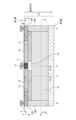
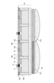
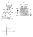
図1は、本実施形態に係るアバランシェダイオードの断面模式図である。本実施形態のアバランシェダイオードは、半導体基板15(第1基板)に配される。半導体基板15は、第1面と、第1面に対向する第2面とを有する。例えば、第1面は半導体基板15の表面であり、第2面は半導体基板15の裏面である。本実施形態では、第1面から第2面へ向かう方向を深さ方向と呼ぶ。半導体基板15の表面側には、トランジスタのゲート電極、多層配線構造等が配される。
Figure 1 is a schematic cross-sectional view of an avalanche diode according to this embodiment. The avalanche diode according to this embodiment is disposed on a semiconductor substrate 15 (first substrate). The
分離部16A、16Bは、半導体領域間を電気的に分離する領域である。分離部16A、16Bは、LOCOS(Local Oxidation Of Silicon)、STI(Shallow Trench Isolation)、DTI(Deep Trench Isolation)等による絶縁分離領域であり得る。また、分離部16A、16Bは、P型半導体領域とN型半導体領域とのPN接合によるPN分離領域であってもよい。
The
図1に示されているように、半導体基板15には、第1の分離領域として機能する分離部16Aによって囲われた領域が形成されている。分離部16Aによって囲われた領域には、第1導電型の第1半導体領域71と、第2半導体領域76とが配されている。更に、半導体基板15には、第2の分離領域として機能する分離部16Bによって囲われた領域が形成されている。分離部16Bによって囲われた領域には、第3半導体領域74と、第2導電型の第4半導体領域72と、第5半導体領域75とが配される。また、半導体基板15の第1面の上には、第1半導体領域71に接するように配されたコンタクトプラグ77が設けられている。コンタクトプラグ77は、アバランシェダイオードの端子として機能する。
As shown in FIG. 1, a region surrounded by an
第1半導体領域71、第2半導体領域76及び分離部16Aは、深さX(第1の深さ)に配される。第1半導体領域71と第2半導体領域76とは、深さ方向に対して垂直な方向(図1中の横方向)に接している。第2半導体領域76は、第1半導体領域71と分離部16Aとの間に配される。
The
ここで、第1半導体領域71、第2半導体領域76及び分離部16Aが深さXに配されるとは、例えば、半導体基板15内に注入された不純物濃度が最も高い領域(ピーク)が深さXであることをいう。しかしながら、これはピークが深さXに厳密に一致していることを意味するものではなく、ピークが深さXから設計誤差、製造誤差等によりずれている場合もピークが深さXに配されている状態に含まれるものとする。
Here, the
第3半導体領域74及び第4半導体領域72は、第1面に対して深さXよりも深い深さYに配される。第5半導体領域75は、第1面に対して深さYよりも深い深さZ(第2の深さ)に配される。分離部16Bは、深さY及び深さZに配される。第3半導体領域74と第4半導体領域72とは深さ方向に対して垂直な方向に接している。第4半導体領域72は、第3半導体領域74と分離部16Bとの間に配される。第5半導体領域75と分離部16Bとは深さ方向に対して垂直な方向に接している。
The
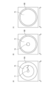
図2(a)、図2(b)及び図2(c)は、本実施形態に係るアバランシェダイオードの平面模式図である。図2(a)、図2(b)及び図2(c)は、それぞれ、深さX、深さY及び深さZにおける平面模式図を示している。 2(a), 2(b), and 2(c) are schematic plan views of the avalanche diode according to this embodiment. 2(a), 2(b), and 2(c) show schematic plan views at depths X, Y, and Z, respectively.
図2(a)に示されるように、深さXにおいて、第1半導体領域71は、第2半導体領域76に内包される。また、第2半導体領域76は、分離部16Aに内包される。なお、図2(a)の距離Rは、第1半導体領域71と分離部16Aとの間の距離を示している。
As shown in FIG. 2(a), at a depth X, the
図2(b)に示されるように、深さYにおいて、第3半導体領域74は、第4半導体領域72に内包される。また、第4半導体領域72は、分離部16Bに内包される。図2(c)に示されるように、深さZにおいて、第5半導体領域75は、分離部16Bに内包される。
As shown in FIG. 2(b), at depth Y, the
図1、図2(a)、図2(b)及び図2(c)に示されるように、平面視において、第1半導体領域71は、第3半導体領域74の少なくとも一部と重なる。また、平面視において、第3半導体領域74及び第4半導体領域72は、第5半導体領域75の少なくとも一部と重なる。更に、平面視において、第2半導体領域76は、第4半導体領域72の少なくとも一部と重なる。ここで、分離部16Aと分離部16Bの平面視における形状は互いに異なる。
As shown in Figures 1, 2(a), 2(b), and 2(c), in a planar view, the
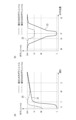
図3(a)及び図3(b)は、本実施形態に係るアバランシェダイオードのポテンシャルの一例を示すグラフである。図3(a)は、図1に示される断面図の線分JK及び線分GHにおけるポテンシャルの分布を示している。図3(b)は、図1に示される断面図の線分AB及び線分CDにおけるポテンシャルの分布を示している。半導体領域内のポテンシャルは、コンタクトプラグ77に印加される電位により変化する。図3(a)及び図3(b)に示すポテンシャルは、アバランシェダイオードに逆バイアス電圧が印加されるように電位が供給されている場合のものである。この電位は、アバランシェダイオードの外部に設けられた電源電圧線から、クエンチ回路等の回路を介して供給される。また、電位のレベルは、アバランシェダイオードでアバランシェ増倍が生じるように設定されている。
3(a) and 3(b) are graphs showing an example of the potential of the avalanche diode according to this embodiment. FIG. 3(a) shows the distribution of potential at the lines JK and GH in the cross-sectional view shown in FIG. 1. FIG. 3(b) shows the distribution of potential at the lines AB and CD in the cross-sectional view shown in FIG. 1. The potential in the semiconductor region changes depending on the potential applied to the
図3(a)において、破線20は、線分GHにおけるポテンシャル分布を示しており、実線21は、線分JKにおけるポテンシャル分布を示している。これらのポテンシャルは、信号電荷である電子についてのポテンシャルを示している。なお、信号電荷が正孔である場合にはポテンシャルの高低の関係が逆になる。横軸の深さX、Y、Z、Wは、図1に示されている対応する符号が付された位置の深さに対応している。すなわち、図3(a)のX、Y、Zはそれぞれ、図1に示した深さX、深さY及び深さZを示している。また、深さWは深さYと深さZとの間の深さである。
In FIG. 3(a), dashed
図3(a)のポテンシャルの各レベルについて説明する。XHレベルは、第4半導体領域72のポテンシャルを示している。Hレベルは、第3半導体領域74のポテンシャルを示している。Mレベルは、第2半導体領域76のポテンシャルを示している。Lレベルは、第1半導体領域71のポテンシャルを示している。なお、第3半導体領域74のポテンシャルよりも第2半導体領域76のポテンシャルの方が低いものとしているが逆であってもよい。また、第4半導体領域72のポテンシャルよりも第3半導体領域74のポテンシャルの方が低いものとしているが同一であってもよい。また、第2半導体領域76のポテンシャルよりも第1半導体領域71のポテンシャルの方が低いものとしているが同一であってもよい。
Each level of the potential in FIG. 3(a) will be explained. The XH level indicates the potential of the
破線20により示されている線分GHにおけるポテンシャルについて説明する。深さZにおいて、ポテンシャルは、XHレベルとHレベルの間である。深さZから深さWに向かうにつれて徐々にポテンシャルは低下する。そして、深さWから深さYに向かうにつれて徐々にポテンシャルが上昇し、深さYにおいてXHレベルとなる。更に、深さYから深さXに向かうにつれて徐々にポテンシャルが低下する。深さX近傍において、ポテンシャルはMレベルとなる。
The potential at the line segment GH indicated by the dashed
アバランシェダイオードを通過する実線21により示されている線分JKにおけるポテンシャルについて説明する。深さZにおいて、ポテンシャルは、XHレベルとHレベルの間である。深さZから深さYに向かうにつれて徐々にポテンシャルは低下し、深さYの近傍でポテンシャルの傾きが大きくなる。そして、ポテンシャルは、深さYにおいて、Hレベルとなる。深さYから深さXに向かうにつれて、ポテンシャルは急激に低下する。すなわち、深さYから深さXの間に急峻なポテンシャル勾配が形成されている。深さXにおいて、ポテンシャルはLレベルとなる。
The potential at the line segment JK indicated by the
深さZにおいて、線分GH及び線分JKにおけるポテンシャルはほぼ同一となっている。また、深さZの近傍において、線分GH及び線分JKの位置では、半導体基板15の第1面の側に向かって緩やかに低下するポテンシャル勾配が形成されている。そのため、入射光により画素内の半導体領域で生成された電荷は、このポテンシャル勾配によって第1面の側に向かって移動する。
At depth Z, the potentials at line segments GH and JK are almost the same. Furthermore, near depth Z, at the positions of line segments GH and JK, a potential gradient is formed that gradually decreases toward the first surface side of
線分JKにおいて、深さWから深さYに近づくにつれて半導体基板15の第1面の側に向かって緩やかに低下するポテンシャル勾配が形成されている。これにより、電荷は第1面の側に向かって移動する。一方、線分GHにおいては、深さWから深さYに近づくにつれて、半導体基板15の第1面の側に向かって緩やかに上昇するポテンシャル勾配が形成されている。このポテンシャル勾配は、第1面に向かう電荷に対するポテンシャル障壁となる。このポテンシャル障壁(第4半導体領域72)は、第5半導体領域75から第2半導体領域76に電荷が移動することを抑制する。これに対し、線分GHの位置から線分JKへの横方向のポテンシャル勾配は小さいため、深さWから深さYの範囲において、線分GHの近傍に存在する電荷は、第1面に向かって移動する過程で線分JKの付近に移動しやすくなる。
In the line segment JK, a potential gradient is formed that gradually decreases toward the first surface side of the
線分JKで示した領域の近傍に移動した電荷は、深さYから深さXの範囲にかけて形成されている急峻なポテンシャル勾配、すなわち強電界によって加速される。強電界によって加速された電荷は、第1半導体領域71に到達する。このようにして、線分JKの近傍の深さYから深さXの領域においてアバランシェ増倍が起こる。これに対し、線分GHに示した領域においては、線分JKの深さYから深さXの領域よりもアバランシェ増倍が起きにくいポテンシャル分布となっている。
The charge that moves to the vicinity of the region indicated by line segment JK is accelerated by the steep potential gradient, i.e., the strong electric field, formed in the range from depth Y to depth X. The charge accelerated by the strong electric field reaches the
このような構造を実現する一例として、第1半導体領域71のポテンシャルと第3半導体領域74のポテンシャルとの差を、第2半導体領域76のポテンシャルと第4半導体領域72のポテンシャルとの差よりも大きくする構成が挙げられる。このようなポテンシャル構造とすることにより、アバランシェダイオードにおいてアバランシェ増倍が起こる構成が実現される。また、この構成では、アバランシェ増倍が起きにくい部分があることに起因する感度の低下も以下の理由により軽減されている。
One example of how such a structure can be achieved is a configuration in which the difference between the potential of the
第3半導体領域74のポテンシャルは、第4半導体領域72のポテンシャルよりも低い。そのため、第4半導体領域72は、第5半導体領域75に存在する信号電荷に対するポテンシャル障壁として機能する。これにより、第5半導体領域75のうちの第4半導体領域72又は第3半導体領域74に重なる領域に存在する信号電荷が、第3半導体領域74を介して第1半導体領域71に移動しやすくなり、電荷が集められるため感度低下が軽減される。
The potential of the
図3(a)には、第3半導体領域74がP型半導体領域である場合のポテンシャル構造が示されている。しかしながら、第3半導体領域74がN型半導体領域である場合であっても、線分GH、線分JKのそれぞれについて深さYにおけるポテンシャルの大小関係は変わらない。すなわち、深さYにおいて、線分GHにおけるポテンシャルは、線分JKにおけるポテンシャルよりも高い。
Figure 3(a) shows the potential structure when the
また、図3(a)では、第2半導体領域76がN型半導体領域である場合のポテンシャル構造が示されているが、P型半導体領域であっても、線分GH、線分JKのそれぞれについて深さYにおけるポテンシャルの大小関係は変わらない。すなわち、深さYにおいて、線分GHにおけるポテンシャルは、線分JKにおけるポテンシャルよりも高い。
In addition, FIG. 3(a) shows the potential structure when the
なお、第5半導体領域75の各部分において生じた電荷は、線分JKで示した領域付近に移動してアバランシェ増倍を起こすため、1つの画素の感度は、分離部16Bに内包される第5半導体領域75の平面視における面積におおよそ比例する。
The charge generated in each part of the
図3(b)において、破線22は、線分CD、すなわち深さYにおけるポテンシャル分布を示しており、実線23は、線分AB、すなわち深さXにおけるポテンシャル分布を示している。XHレベル、Hレベル、Mレベル、Lレベルの意味は図3(a)と同様であるため説明を省略する。
In FIG. 3(b), dashed line 22 indicates the potential distribution at line segment CD, i.e., depth Y, and
破線22により示されるポテンシャルは、水平位置に応じてXHレベルとHレベルの間で変化する。第3半導体領域74の近傍においてポテンシャルが低くなっている。実線23により示されるポテンシャルは、水平位置に応じてXHレベルとLレベルの間で変化する。より具体的には、分離部16Aから第1半導体領域71に近づくにつれて徐々にポテンシャルが低くなる分布となっている。分離部16Aと第1半導体領域71との間に位置する第2半導体領域76のポテンシャルは、分離部16Aから第1半導体領域71に向かって緩やかに変化する。このポテンシャル分布は、第2半導体領域76の不純物濃度が比較的低濃度になるように不純物の注入を行うことにより実現され得る。
The potential indicated by the dashed line 22 varies between the XH level and the H level depending on the horizontal position. The potential is low in the vicinity of the
本実施形態では、分離部16Aと第1半導体領域71との間に第2半導体領域76を配置することにより、分離部16Aと第1半導体領域71との間が一定の距離Rだけ離されている。これにより、第1半導体領域71のポテンシャルと第3半導体領域74のポテンシャルの差による電界の強度に比べて、分離部16Aのポテンシャルと第1半導体領域71のポテンシャルの差による電界の強度を低くすることができる。したがって、分離部16Aと第1半導体領域71とのPN接合において発生するアバランシェ増倍によってトンネル効果によるノイズが生じることが抑制される。
In this embodiment, the
以上のように、深さXに配された分離部16Aは、信号電荷によるアバランシェ増倍が生じるアバランシェ領域(第2領域)を画定している。また、深さZに配された分離部16Bは、入射光を光電変換することにより信号電荷を生成する感度領域(第1領域)を画定している。上述のように、深さXの分離部16Aは、トンネル効果によるノイズを低減する観点から、分離部16Aと第1半導体領域71との間の距離Rをある程度確保するように設計される。これに対し、深さZの分離部16Bは、各画素の感度領域の位置及び感度の大きさが所望のものになるように形状、面積等を調整して設計される。このように、アバランシェ領域の形状と感度領域の形状とは、設計制約が互いに異なるため、これらは互いに異なる形状が最適となる場合がある。そこで、本実施形態では、平面視において、分離部16Aの形状と、分離部16Bの形状とが互いに異なっている。これにより、レイアウトの自由度が向上された光電変換装置が提供され、アバランシェ領域の形状と感度領域の形状とをそれぞれの性質に適した形状に設計することができる。
As described above, the
分離部16Aの形状と、分離部16Bの形状とが互いに異なっている構成の一例として、分離部16Aに内包される面積と分離部16Bに内包される面積を異ならせてもよい。例えば、感度を大きくしたい画素については分離部16Aに内包される面積に比して分離部16Bに内包される面積を大きくすることにより、分離部16Bが隣接した画素の一部に重なるよう配置されてもよい。上述のように本実施形態のアバランシェダイオードにおいては、第5半導体領域75に存在する信号電荷は、第3半導体領域74を介して第1半導体領域71に移動しやすい。したがって、第5半導体領域75で生じた信号電荷は第1半導体領域71に集められるため、分離部16Aに内包される面積に比して分離部16Bに内包される面積を大きくした場合であっても、同様にアバランシェ増倍が起こる。一部の画素の分離部16Bに内包される面積を大きくした構成の例を図4に示す。
As an example of a configuration in which the shape of the
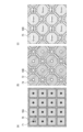
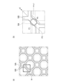
図4(a)、図4(b)及び図4(c)は、一部の画素において、分離部16Aに内包される面積よりも分離部16Bに内包される面積を大きくした画素配列の例を示す平面模式図である。図4(a)は、深さXにおける平面模式図であり、図4(b)は、深さYにおける平面模式図であり、図4(c)は、深さZにおける平面模式図である。これらの図に示されるように、半導体基板15に配された複数の画素は、複数の行及び複数の列をなすように配列されている。図4(a)、図4(b)及び図4(c)には、複数の画素のうちの4行×4列分が抜き出されて示されている。
Figures 4(a), 4(b), and 4(c) are schematic plan views showing an example of a pixel array in which the area enclosed by
図4(a)に示されるように、深さXにおいて、第1半導体領域71は、第2半導体領域76に内包される。また、第2半導体領域76は、分離部16Aに内包される。第1半導体領域71と分離部16Aの間の最小距離は、いずれの画素においても距離Rである。
As shown in FIG. 4(a), at a depth X, the
図4(b)に示されるように、深さYにおいて、第3半導体領域74は、第4半導体領域72に内包される。また、第4半導体領域72は、分離部16Bに内包される。図4(c)に示されるように、深さZにおいて、第5半導体領域75は、分離部16Bに内包される。図4(c)の第5半導体領域75内に示されている「Red」、「Green」、「Blue」の文字は、対応する画素が、それぞれ、赤色画素、緑色画素、青色画素であることを示している。赤色画素、緑色画素、青色画素は、それぞれ、赤色、緑色、青色のカラーフィルタが設けられている画素である。本実施形態において、赤色画素、緑色画素、青色画素は、ベイヤー配列をなしている。
As shown in FIG. 4(b), at depth Y, the
図4(c)に示されるように、本実施形態では緑色画素の分離部16Bに内包される面積が他の色の画素のそれよりも大きい。これを実現するため、緑色画素の分離部16Bは、平面視において、隣接する赤色画素又は青色画素との間の分離部16Aに対して外側に超えるように配されている。言い換えると、平面視において、分離部16Aの形状と、分離部16Bの形状とが互いに異なっている。これにより、緑色画素の感度領域の面積を他の色の画素の感度領域の面積よりも広くすることができ、緑色画素の感度を大きくすることができる。人間の目の感度は、赤色又は青色よりも緑色に対して強いことから、図4(c)のように緑色画素の感度領域の面積を赤色画素又は青色画素の感度領域の面積よりも広くすることにより、実質的な画質が向上する。
As shown in FIG. 4(c), in this embodiment, the area included in the
なお、設計要求によっては、緑色画素以外の色の画素を大きくする構成であってもよい。すなわち、より一般的な形で言い換えると、光電変換装置に含まれる2つのアバランシェダイオードについて、分離部16Bにより囲まれる感度領域の面積が互いに異なっていてもよい。そして、この2つのアバランシェダイオードは、第1の色の入射光に対して感度を有する第1のアバランシェダイオードと、第1の色とは異なる第2の色の入射光に対して感度を有する第2のアバランシェダイオードと言い換えることができる。
Depending on design requirements, the pixels of colors other than the green pixel may be enlarged. In other words, in more general terms, the areas of the sensitivity regions surrounded by the
図5(a)及び図5(b)を参照して、分離部16Aと分離部16Bの位置関係をより詳細に説明する。図5(a)は、図4(a)の分離部16Aと図4(b)の分離部16Bとを重ねて示した平面模式図である。図5(b)は、分離部16Aと分離部16Bとの交差部Wの拡大図である。図5(b)に示されるように、分離部16Aは、x1方向(第1の方向)に延在する第1部分P1を含む。また、分離部16Bは、x1方向に対して平面視で交差するx2方向(第2の方向)に延在する第2部分P2を含む。このとき、平面視において、第1部分P1の一部と第2部分P2の一部とが、重畳部P3において互いに重なっている。
The positional relationship between the
以上のように、本実施形態によれば、平面視において、アバランシェ領域の間を分離する分離部16Aの形状と、感度領域の間を分離する分離部16Bの形状とが互いに異なっている。より具体的には、平面視において、分離部16Aの第1部分P1の一部と分離部16Bの第2部分P2の一部とが重畳部P3において互いに重なっている。これにより、レイアウトの自由度が向上された光電変換装置が提供される。
As described above, according to this embodiment, in a plan view, the shape of the
また、本実施形態によれば、第3の分離領域として機能する第4半導体領域72が、アバランシェ領域と感度領域との間の一部を分離するように配されている。これにより、第5半導体領域75に存在する信号電荷が、第3半導体領域74を介して第1半導体領域71に移動しやすくなるため感度が向上される。
In addition, according to this embodiment, the
本実施形態の説明において、アバランシェダイオードに印加されるバイアス電圧はアバランシェ増倍が生じる状態になるように制御されているものとしているが、これだけでなくアバランシェ増倍が生じない状態にも制御可能であってもよい。言い換えると、本実施形態のアバランシェダイオードは、信号電荷を感度領域に蓄積する蓄積モードと、感度領域に蓄積された信号電荷を読み出す読み出しモードと、の2種のモードにより動作可能であってもよい。ここで、蓄積モードとは、アバランシェダイオードに第1のバイアス電圧が印加され、アバランシェ増倍が生じない状態に制御されるモードである。アバランシェダイオードが蓄積モードであるときに光電変換により生じた電荷は、感度領域内に蓄積される。読み出しモードとは、第1のバイアス電圧とは異なる第2のバイアス電圧が印加され、アバランシェ増倍が生じる状態に制御されるモードである。このようにアバランシェダイオードが2種のモードで制御されることにより、感度領域に所定時間だけ信号電荷を蓄積してから、所定時間内に蓄積された信号電荷に応じた信号を読み出すような動作が実現可能となる。 In the description of this embodiment, the bias voltage applied to the avalanche diode is controlled so that avalanche multiplication occurs, but it may also be controlled so that avalanche multiplication does not occur. In other words, the avalanche diode of this embodiment may be operable in two modes: an accumulation mode in which signal charges are accumulated in the sensitivity region, and a readout mode in which the signal charges accumulated in the sensitivity region are read out. Here, the accumulation mode is a mode in which a first bias voltage is applied to the avalanche diode and the avalanche diode is controlled to a state in which avalanche multiplication does not occur. When the avalanche diode is in the accumulation mode, the charge generated by photoelectric conversion is accumulated in the sensitivity region. The readout mode is a mode in which a second bias voltage different from the first bias voltage is applied and the avalanche diode is controlled to a state in which avalanche multiplication occurs. In this way, the avalanche diode is controlled in two modes, so that an operation in which signal charges are accumulated in the sensitivity region for a predetermined time and then a signal corresponding to the signal charges accumulated within the predetermined time can be realized.
[第2実施形態]
第2実施形態に係る光電変換装置について説明する。本実施形態の説明において、第1実施形態と同様の機能を有する部分には同様の符号を付し、詳細な説明を省略又は簡略化することもある。
[Second embodiment]
A photoelectric conversion device according to a second embodiment will be described below. In the description of this embodiment, parts having the same functions as those in the first embodiment will be denoted by the same reference numerals, and detailed description thereof may be omitted or simplified.
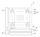
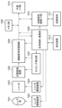
図6は、本実施形態に係る光電変換装置10のブロック図である。光電変換装置10は、画素部106、制御パルス生成部109、水平走査回路104、列回路105、信号線107、出力回路108及び垂直走査回路103を有している。
Figure 6 is a block diagram of a
画素部106は、複数の行及び複数の列をなすように配された複数の画素100を有している。各々の画素100は、光電変換素子101及び画素信号処理部102を含む。光電変換素子101は、光電変換装置10に入射された光を電気信号に変換する。画素信号処理部102は、当該電気信号を信号線107を介して列回路105に出力する。
The
垂直走査回路103は、制御パルス生成部109から供給された制御パルスに基づいて各画素100を画素行ごとに駆動するための制御パルスを供給する。垂直走査回路103には、シフトレジスタ、アドレスデコーダ等の論理回路が用いられ得る。信号線107は、画素部106の列ごとに配されている。信号線107は、垂直走査回路103により選択された画素100から出力された信号を列回路105に伝送する。
The
列回路105には、信号線107を介して各画素100の信号が入力される。列回路105は入力された信号に対して、所定の処理を行う。所定の処理とは、入力された信号のノイズ除去、増幅等の処理と、処理後の信号を外部に出力する形に変換する処理を含み得る。この機能を実現するため、例えば、列回路105は、パラレル-シリアル変換回路を有する。
The signal of each
水平走査回路104は、列回路105で処理された後の信号を出力回路108に列ごとに順次出力するための制御パルスを列回路105に供給する。出力回路108は、バッファアンプ、差動増幅器等から構成される。出力回路108は、列回路105から出力された信号を光電変換装置10の外部の記憶部又は信号処理部に出力する。
The
図6において、画素部106における画素100の配列は、2次元行列状であるがこれに限定されるものではない。例えば、画素部106は、複数の画素100が1次元状に配されるものであってもよい。また、画素部106に含まれる画素100は単一であってもよい。また、垂直走査回路103、水平走査回路104及び列回路105は、複数のブロックに分割されていてもよく、画素部106のブロックが上述の垂直走査回路103、水平走査回路104及び列回路105のブロックと対応するように配置されていてもよい。また、水平走査回路104及び列回路105は、各画素列に対応するブロックに分割されていてもよい。
In FIG. 6, the arrangement of the
画素信号処理部102の機能が画素部106内のすべての画素100に1つずつ設けられることは必須ではなく、例えば、複数の画素100によって1つの画素信号処理部102が共有されていてもよい。この場合、画素信号処理部102は、複数の画素100から出力される信号に対して順次処理を行う。
It is not essential that the functions of the pixel
また、図6において、光電変換素子101が2次元状に配列された画素アレイを含む半導体基板15と、それ以外の要素を含む半導体基板が別の半導体基板であってもよい。これにより、チップ面積に対する光電変換素子101の面積の割合を高くすることができ、光電変換素子101の感度が向上する。この場合、光電変換装置10は、複数の半導体基板同士を貼り合せた積層構造であり得る。
Also, in FIG. 6, the
この構成の一例として、画素信号処理部102は、光電変換素子101が形成される半導体基板15とは異なる半導体基板に設けられていてもよい。この場合、光電変換素子101と画素信号処理部102とは、画素100ごとに設けられた接続配線を介して互いに電気的に接続される。垂直走査回路103、水平走査回路104、信号線107及び列回路105も同様に光電変換素子101とは異なる半導体基板に設けられていてもよく、同様の効果が得られる。
As an example of this configuration, the pixel
図7は本実施形態に係る画素100のブロック図の一例である。図7において、1つの画素100は、光電変換素子101及び画素信号処理部102を有する。光電変換素子101は、光電変換部201及び制御部202を有する。
Figure 7 is an example of a block diagram of a
光電変換部201は、光電変換により入射光に応じた電荷対を生成する。光電変換部201には、アバランシェダイオードが用いられる。光電変換部201のアノードは、電位VLを供給する電位線に接続される。光電変換部201のカソードは、制御部202の一端に接続される。制御部202の他端は、電位VLよりも高い電位VHを供給する電位線に接続される。
The
このような構成により、光電変換部201のアノードとカソードには、アバランシェ増倍が生じ得るような逆バイアスの電位が印加される。このような逆バイアスの電位が印加された状態で入射光による光電変換が行われると、生成された電荷がアバランシェ増倍を起こしアバランシェ電流が発生する。
With this configuration, a reverse bias potential that can cause avalanche multiplication is applied to the anode and cathode of the
なお、光電変換部201に逆バイアスの電位が供給される場合において、アノードとカソードの電位差が降伏電圧よりも大きいときには、アバランシェダイオードはガイガーモード動作となる。ガイガーモード動作を用いて単一光子レベルの微弱信号を高速検出するフォトダイオードがSPAD(Single Photon Avalanche Diode)である。
When a reverse bias potential is supplied to the
また、光電変換部201のアノードとカソードの電位差が、光電変換部201に生じた電荷がアバランシェ増倍を起こす電位差以上であって、かつ降伏電圧以下の電位差である場合には、アバランシェダイオードは線形モードになる。線形モードにおいて光検出を行うアバランシェダイオードをアバランシェフォトダイオード(APD)と呼ぶ。本実施形態において、光電変換部201はどちらのアバランシェダイオードとして動作してもよい。なお、アバランシェ増倍を起こす電位差はおよそ6V以上である。
In addition, when the potential difference between the anode and cathode of the
制御部202は、光電変換部201で生じたアバランシェ電流の変化を電圧信号に置き換える機能を有する。更に、制御部202は、アバランシェ増倍による信号増幅時に負荷回路(クエンチ回路)として機能する。この負荷回路は、光電変換部201に供給する電圧を変化させて、アバランシェ増倍を抑制するクエンチ動作を行う。制御部202は、例えば、抵抗素子又は能動クエンチ回路を含み得る。能動クエンチ回路は、アバランシェ電流の増加を検出してフィードバック制御を行うことによりアバランシェ増倍を能動的に抑制する回路である。
The
画素信号処理部102は、波形整形部203、カウンタ回路204及び選択回路206を有する。波形整形部203は、単一光子レベルの信号による電圧変化を整形して、パルス信号を出力する。このパルス信号は光子の入射を示すものである。波形整形部203には、例えば、図7に示されているようにインバータ回路が用いられる。図7には、波形整形部203として、1つのインバータを用いた例が示されているが、波形整形部203は、複数のインバータを直列接続した回路であってもよく、波形整形効果がある回路であればその他の回路であってもよい。
The pixel
波形整形部203から出力されたパルス信号は、カウンタ回路204によってカウントされる。カウンタ回路204には、例えば、N-bitカウンタ(N:正の整数)が備えられており、N-bitカウンタは、入力されたパルス信号を最大で約2のN乗個までカウントしてその値を保持することが可能である。カウントにより得られた信号は、入射光の検出結果を示す信号としてカウンタ回路204に保持される。また、カウンタ回路204には、垂直走査回路103から駆動線207を介して制御パルスpRESが供給される。カウンタ回路204は、制御パルスpRESが入力されると保持している信号をリセットする。
The pulse signal output from the
選択回路206には、垂直走査回路103から駆動線208を介して制御パルスpSELが供給される。選択回路206は、制御パルスpSELに基づいてカウンタ回路204と信号線107との電気的な接続又は非接続を切り替える。選択回路206には、例えばトランジスタ、画素外に信号を出力するためのバッファ回路等が用いられ得る。
The
画素部106が複数の画素100が行列状に配された構成である場合において、撮像動作は、ローリングシャッタ動作及びグローバル電子シャッタ動作のいずれであってもよい。例えば、カウンタ回路204によるカウントを行ごとに順次リセットし、カウンタ回路204に保持された信号を行ごとに順次出力することによりローリングシャッタ動作が実現される。
When the
また、すべての画素行のカウンタ回路204によるカウントを同時にリセットし、カウンタ回路204に保持された信号を行ごとに順次出力することにより、グローバル電子シャッタ動作が実現される。なお、グローバル電子シャッタ動作を適用する場合には、カウンタ回路204によるカウントを行うか否かを切り替えることができるように、スイッチ等による切替手段を設けることが望ましい。
In addition, the counts by the
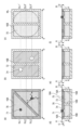
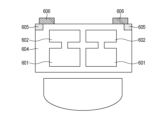
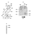
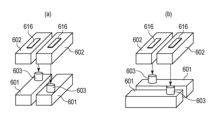
図8(a)乃至図8(f)は、図6及び図7のアバランシェダイオードがほぼ正方形の領域内に対角状に2つ配置された構成の例を示す平面模式図及び断面模式図である。光電変換装置10の複数のアバランシェダイオードは、図8(a)乃至図8(f)に示した2つのアバランシェダイオードを一単位として複数の行及び複数の列をなして行列状に配されている。図8(a)は、深さXにおける平面模式図であり、図8(b)は、深さYにおける平面模式図であり、図8(c)は、深さZにおける平面模式図である。また、図8(d)は線分SL1-SL1’における断面模式図であり、図8(e)は線分SL2-SL2’における断面模式図であり、図8(f)は線分SL3-SL3’における断面模式図である。
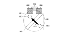
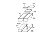
FIGS. 8(a) to 8(f) are schematic plan views and schematic cross-sectional views showing an example of a configuration in which two avalanche diodes of FIGS. 6 and 7 are arranged diagonally within a substantially square region. The multiple avalanche diodes of the
図8(a)に示されるように、深さXにおいて、2つの第1半導体領域71は、それぞれ、2つの第2半導体領域76に内包される。また、2つの第2半導体領域76は、それぞれ、分離部16Aの異なる部分に内包される。第1半導体領域71と分離部16Aとの距離は、いずれの方向にも距離Rとなるように配置される。言い換えると、第1半導体領域71と分離部16Aとの距離が最大となるように第1半導体領域71が配されている。2つの第1半導体領域71は、分離部16Aがなす正方形の対角線上に配置される。2つの第1半導体領域71の間には、2つの第2半導体領域76を斜めに分離するように分離部16Aが斜め方向(アバランシェダイオードがなす行と列のいずれとも異なる方向)に延在して配されている。このように、正方形の領域に2つのアバランシェダイオードを配置する場合には、第1半導体領域71を対角線上に配置することにより距離Rを大きくすることができる。これにより、2つの第1半導体領域71を横方向に並べて配置する場合と比べて距離Rを約1.17倍に大きくすることができる。
8(a), at a depth X, the two
図8(b)に示されるように、深さYにおいて、第3半導体領域74は、第4半導体領域72に内包される。また、第4半導体領域72は分離部16Bに内包される。
As shown in FIG. 8(b), at depth Y, the
図8(c)に示されるように、深さZにおいて、2つの第5半導体領域75は、それぞれ、分離部16Bの異なる部分に内包される。2つの第5半導体領域75の間には、2つの第2半導体領域76を横方向に分離するように分離部16Bが縦方向に延在して配されている。また、図8(c)には、2つの第5半導体領域75に入射光を導くマイクロレンズMLの位置が破線で図示されている。2つの第5半導体領域75の位置は、マイクロレンズMLの中心位置に対して横方向に対称に配されている。すなわち、本実施形態の2つのアバランシェダイオードは、1つのマイクロレンズMLに対して光学的に共役関係にある2つの感度領域を有している。これにより、2つのアバランシェダイオードから得られた信号は、位相差オートフォーカス用の信号として用いられ得る。
8(c), at the depth Z, the two
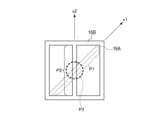
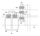
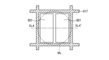
図9を参照して、分離部16Aと分離部16Bの位置関係をより詳細に説明する。図9は、図8(a)の分離部16Aと図8(b)の分離部16Bとを重ねて示した平面模式図である。図9に示されるように、分離部16Aは、x1方向(第1の方向)に延在する第1部分P1を含む。また、分離部16Bは、x1方向に対して平面視で交差するx2方向(第2の方向)に延在する第2部分P2を含む。このとき、平面視において、第1部分P1の一部と第2部分P2の一部とが、重畳部P3において互いに重なっている。
The positional relationship between
このように、本実施形態では、平面視において、分離部16Aの2つの第1半導体領域71を分離する部分と、分離部16Bの2つの第5半導体領域75を分離する部分とが互いに交差している。すなわち、平面視において、分離部16Aの形状と、分離部16Bの形状とが互いに異なっている。より具体的には、平面視において、分離部16Aの第1部分P1の一部と分離部16Bの第2部分P2の一部とが重畳部P3において互いに重なっている。これにより、レイアウトの自由度が向上された光電変換装置10が提供され、アバランシェ領域の形状と感度領域の形状とをそれぞれの性質に適した形状に設計することができる。
Thus, in this embodiment, in a plan view, the portion of
より具体的には、本実施形態の分離部16Aは、正方形の領域に2つのアバランシェダイオードを配置する際の距離Rが最大になるように、斜め方向に延在して配されている。これに対し、本実施形態の分離部16Bは、位相差オートフォーカス用の位相差の取得方向を考慮して、感度領域を図中の横方向に対称に配置する必要性から、縦方向に延在して配されている。言い換えると、アバランシェ領域を画定する分離部16Aと感度領域を画定する分離部16Bは、要求される特性及び設計制約が互いに異なるため、これらは互いに異なる形状に設計されている。このように、分離部16Aの形状と、分離部16Bの形状とを互いに異ならせることにより、距離Rを大きくしてトンネル効果によるノイズを低減する効果と、位相差オートフォーカス用の信号を取得するという要求とを両立することができる。また、2つのアバランシェダイオードを正方形の領域内に斜めに配置することにより、距離Rを大きくすることができるため、距離Rの最大値に制約がある場合には、本実施形態の構成を採用することにより画素のサイズを小型化することができる。これにより、画素数を多くすることができ、得られる画像の品質が向上する効果が得られる。
More specifically, the
なお、本実施形態では分離部16A、16Bの外周形状は、正方形であるが、これに限定されるものではない。例えば、分離部16A、16Bの外周形状が矩形(正方形を含む)であり、2つのアバランシェダイオードが矩形の領域内に配される構成であってもよい。この場合も、分離部16Aは、2つのアバランシェダイオードを配置する際の距離Rが最大になるように、対角線方向に延在して配される。
In this embodiment, the outer periphery of the
[第3実施形態]
第3実施形態に係る光電変換装置について説明する。本実施形態の説明において、第1実施形態又は第2実施形態と同様の機能を有する部分には同様の符号を付し、詳細な説明を省略又は簡略化することもある。
[Third embodiment]
A photoelectric conversion device according to a third embodiment will be described. In the description of this embodiment, parts having the same functions as those in the first or second embodiment are denoted by the same reference numerals, and detailed description thereof may be omitted or simplified.
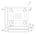
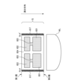
本実施形態の光電変換装置は、第2実施形態の光電変換装置を裏面照射型の光電変換装置に適用したものである。図10は、本実施形態に係る光電変換装置の断面模式図である。図10は、図8の線分SL1-SL1’における断面模式図にカラーフィルタCF1、CF2とマイクロレンズMLとを追加して示したものである。図10に示されるように、カラーフィルタCF1、CF2とマイクロレンズMLとは、半導体基板15の第2面側に配される。
The photoelectric conversion device of this embodiment is the photoelectric conversion device of the second embodiment applied to a back-illuminated photoelectric conversion device. FIG. 10 is a schematic cross-sectional view of the photoelectric conversion device of this embodiment. FIG. 10 shows the schematic cross-sectional view of the line segment SL1-SL1' in FIG. 8 with color filters CF1, CF2 and microlens ML added. As shown in FIG. 10, color filters CF1, CF2 and microlens ML are arranged on the second surface side of
入射光は、マイクロレンズML及びカラーフィルタCF1、CF2を順に通過し、半導体基板15の第2面側から入射される。カラーフィルタCF1、CF2は、互いに異なる色の光を通過させる。マイクロレンズMLは、2つのアバランシェダイオードに共有されており、マイクロレンズMLを通過した光は、2つのアバランシェダイオードのいずれかに導かれる。なお、図10では、1つのマイクロレンズMLが2つのアバランシェダイオードに対応して配されているが、これに限定されるものではない。すなわち、1つのマイクロレンズMLは、2以上のアバランシェダイオードに対応して配され得る。
Incoming light passes through the microlens ML and color filters CF1 and CF2 in order, and is incident on the second surface side of the
以上のように、本実施形態の光電変換装置は、配線層が設けられる第1面とは逆の第2面が受光面となっている裏面照射型である。これにより、本実施形態の光電変換装置は、表面照射型の場合と比べて感度がより向上される。 As described above, the photoelectric conversion device of this embodiment is a back-illuminated type in which the second surface opposite to the first surface on which the wiring layer is provided is the light receiving surface. This improves the sensitivity of the photoelectric conversion device of this embodiment compared to the front-illuminated type.
[第4実施形態]
第4実施形態に係る光電変換装置について説明する。本実施形態の説明において、第1実施形態乃至第3実施形態と同様の機能を有する部分には同様の符号を付し、詳細な説明を省略又は簡略化することもある。
[Fourth embodiment]
A photoelectric conversion device according to a fourth embodiment will be described. In the description of this embodiment, parts having the same functions as those in the first to third embodiments are denoted by the same reference numerals, and detailed description thereof may be omitted or simplified.
本実施形態の光電変換装置は、第3実施形態の光電変換装置を積層型の光電変換装置に適用したものである。図11は、本実施形態に係る光電変換装置の断面模式図である。図11は、図8の線分SL1-SL1’における断面模式図にカラーフィルタCF1、CF2と、マイクロレンズMLと、半導体基板17とを追加して示したものである。第3実施形態と同様に、カラーフィルタCF1、CF2とマイクロレンズMLとは、半導体基板15の第2面側に配される。また、半導体基板17は、接合面18を介して半導体基板15の第1面側に接合され、半導体基板15と機械的及び電気的に接続される。半導体基板17には、画素信号処理部102等のアバランシェダイオードから出力された信号を処理する信号処理回路が含まれる。
The photoelectric conversion device of this embodiment is a stacked type photoelectric conversion device applied to the photoelectric conversion device of the third embodiment. FIG. 11 is a schematic cross-sectional view of the photoelectric conversion device of this embodiment. FIG. 11 shows the schematic cross-sectional view of the line segment SL1-SL1' in FIG. 8 with the addition of color filters CF1 and CF2, a microlens ML, and a
以上のように、本実施形態の光電変換装置は、第3実施形態と同様の裏面照射型であることに加えて、半導体基板15(第1基板)と半導体基板17(第2基板)とが積層された積層型である。半導体基板15には、アバランシェダイオードが配されており、半導体基板17には、信号処理回路が配されている。これにより、アバランシェダイオードと信号処理回路とが同一基板に配されている場合と比べてアバランシェダイオードの感度領域を広くすることができ、感度がより向上される。
As described above, the photoelectric conversion device of this embodiment is a back-illuminated type similar to the third embodiment, and is also a stacked type in which semiconductor substrate 15 (first substrate) and semiconductor substrate 17 (second substrate) are stacked. An avalanche diode is disposed on
[第5実施形態]
第5実施形態に係る光電変換装置について説明する。本実施形態の説明において、第1実施形態乃至第4実施形態と同様の機能を有する部分には同様の符号を付し、詳細な説明を省略又は簡略化することもある。本実施形態の光電変換装置は、第1実施形態乃至第4実施形態とは異なり、アバランシェ増倍を利用しないフォトダイオードを用いたイメージセンサである。本実施形態の光電変換装置は、撮像用の信号を出力する機能だけでなく像面位相差オートフォーカス用の信号を出力する機能を有している。
[Fifth embodiment]
A photoelectric conversion device according to a fifth embodiment will be described. In the description of this embodiment, parts having the same functions as those of the first to fourth embodiments are given the same reference numerals, and detailed description may be omitted or simplified. The photoelectric conversion device according to this embodiment is an image sensor using a photodiode that does not use avalanche multiplication, unlike the first to fourth embodiments. The photoelectric conversion device according to this embodiment has not only a function of outputting a signal for imaging, but also a function of outputting a signal for image plane phase difference autofocus.
図12は、本実施形態に係る光電変換装置60のブロック図である。光電変換装置60は、画素部61、制御パルス生成部109、水平走査回路104、列回路105、信号線107、出力回路108及び垂直走査回路103を有している。制御パルス生成部109、水平走査回路104、列回路105、信号線107、出力回路108及び垂直走査回路103の構成は第2実施形態と概ね同様であるため説明を省略する。
Figure 12 is a block diagram of a
画素部61は、複数の行及び複数の列をなすように配された複数の画素600を有している。各々の画素600は、入射された光を電気信号に変換するフォトダイオードを有している。
The
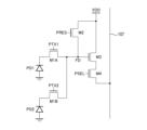
図13は本実施形態に係る画素600の等価回路図の一例である。画素600は、光電変換部PD1、PD2、転送トランジスタM1A、M1B、リセットトランジスタM2、増幅トランジスタM3及び選択トランジスタM4を有する。これらのトランジスタはNチャネルMOSトランジスタであり得る。転送トランジスタM1Aのゲートには、垂直走査回路103から制御信号PTX1が入力される。転送トランジスタM1Bのゲートには、垂直走査回路103から制御信号PTX2が入力される。リセットトランジスタM2のゲートには、垂直走査回路103から制御信号PRESが入力される。選択トランジスタM4のゲートには、垂直走査回路103から制御信号PSELが入力される。
Figure 13 is an example of an equivalent circuit diagram of a
光電変換部PD1、PD2は、光電変換により入射光に応じた電荷を生成するとともに、当該電荷を蓄積する。光電変換部PD1、PD2は、第1乃至第4実施形態で述べたようなアバランシェダイオードではなく、アバランシェ増倍を利用していない通常のフォトダイオードである。光電変換部PD1、PD2の各々のアノードは、接地電位線に接続されている。光電変換部PD1のカソードは、転送トランジスタM1Aのソースに接続されている。光電変換部PD2のカソードは、転送トランジスタM1Bのソースに接続されている。 The photoelectric conversion units PD1 and PD2 generate electric charges according to incident light through photoelectric conversion, and accumulate the electric charges. The photoelectric conversion units PD1 and PD2 are not avalanche diodes as described in the first to fourth embodiments, but are normal photodiodes that do not utilize avalanche multiplication. The anodes of the photoelectric conversion units PD1 and PD2 are connected to the ground potential line. The cathode of the photoelectric conversion unit PD1 is connected to the source of the transfer transistor M1A. The cathode of the photoelectric conversion unit PD2 is connected to the source of the transfer transistor M1B.
転送トランジスタM1A、M1Bのドレイン、リセットトランジスタM2のソース及び増幅トランジスタM3のゲートの接続ノードはフローティングディフュージョンFDを構成する。リセットトランジスタM2のドレイン及び増幅トランジスタM3のドレインは、電位VDDを有する電源電位線に接続されている。増幅トランジスタM3のソースは、選択トランジスタM4のドレインに接続されている。選択トランジスタM4のソースは、信号線107に接続されている。信号線107には、不図示の電流源が接続される。
The connection node between the drains of the transfer transistors M1A and M1B, the source of the reset transistor M2, and the gate of the amplification transistor M3 constitutes a floating diffusion FD. The drain of the reset transistor M2 and the drain of the amplification transistor M3 are connected to a power supply potential line having a potential VDD. The source of the amplification transistor M3 is connected to the drain of the selection transistor M4. The source of the selection transistor M4 is connected to a
制御信号PRESがハイレベルになりリセットトランジスタM2がオンになると、フローティングディフュージョンFDの電位がリセットされる。制御信号PTX1がハイレベルになり転送トランジスタM1Aがオンになると、光電変換部PD1に蓄積されている電荷がフローティングディフュージョンFDに転送される。制御信号PTX2がハイレベルになり転送トランジスタM1Bがオンになると、光電変換部PD2に蓄積されている電荷がフローティングディフュージョンFDに転送される。制御信号PSELがハイレベルになり選択トランジスタM4がオンになると、増幅トランジスタM3と信号線107に接続された電流源はソースフォロワ回路を構成する。このとき、フローティングディフュージョンFDの電位に応じた電圧が信号線107に出力される。
When the control signal PRES goes high and the reset transistor M2 turns on, the potential of the floating diffusion FD is reset. When the control signal PTX1 goes high and the transfer transistor M1A turns on, the charge stored in the photoelectric conversion unit PD1 is transferred to the floating diffusion FD. When the control signal PTX2 goes high and the transfer transistor M1B turns on, the charge stored in the photoelectric conversion unit PD2 is transferred to the floating diffusion FD. When the control signal PSEL goes high and the selection transistor M4 turns on, the amplification transistor M3 and the current source connected to the
このような構成により、本実施形態の光電変換装置は、2つの光電変換部PD1、PD2に蓄積されている電荷に基づく信号を個別に出力することができる。また、本実施形態の光電変換装置は、2つの光電変換部PD1、PD2に蓄積されている電荷を加算してこれに基づく信号を出力することもできる。 With this configuration, the photoelectric conversion device of this embodiment can individually output signals based on the charges accumulated in the two photoelectric conversion units PD1 and PD2. The photoelectric conversion device of this embodiment can also add the charges accumulated in the two photoelectric conversion units PD1 and PD2 and output a signal based on the sum.
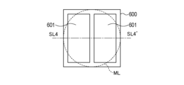
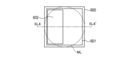
図14は、本実施形態に係るフォトダイオードの平面模式図である。図14はフォトダイオードの一部を構成する2つのN型半導体領域601とマイクロレンズMLの位置関係を示している。図14には、2つのN型半導体領域601に入射光を導くマイクロレンズMLの位置が破線で図示されている。図14の2つのN型半導体領域601は、図13の光電変換部PD1、PD2の感度領域にそれぞれ対応する。2つのN型半導体領域601の位置は、マイクロレンズMLの中心位置に対して横方向に対称に配されている。すなわち、本実施形態の2つのフォトダイオードは、1つのマイクロレンズMLに対して光学的に共役関係にある2つの感度領域を有している。これにより、2つのフォトダイオードから得られた信号は、像面位相差オートフォーカス用の信号として用いられ得る。
14 is a schematic plan view of a photodiode according to this embodiment. FIG. 14 shows the positional relationship between two N-
図15は、本実施形態に係るフォトダイオードの断面模式図である。図15には、図14の線分SL4-SL4’における断面が模式的に示されている。本実施形態のフォトダイオードは、半導体基板15(第1基板)に配される。半導体基板15は、第1面と、第1面に対向する第2面とを有する。例えば、第1面は半導体基板15の表面であり、第2面は半導体基板15の裏面である。本実施形態では、第1面から第2面へ向かう方向を深さ方向と呼ぶ。半導体基板15の表面側には、トランジスタのゲート電極、多層配線構造等が配される。半導体基板15の裏面側には、2つのフォトダイオードに対応するマイクロレンズMLが配される。
Figure 15 is a schematic cross-sectional view of a photodiode according to this embodiment. Figure 15 shows a schematic cross-section along line segment SL4-SL4' in Figure 14. The photodiode according to this embodiment is disposed on a semiconductor substrate 15 (first substrate). The
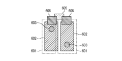
図15に示されているように、半導体基板には、P型半導体領域604と、P型半導体領域604によって囲われた領域が形成されている。P型半導体領域604によって囲われた領域には、N型半導体領域601、602、603が配されている。
As shown in FIG. 15, a P-
N型半導体領域602は、深さD1(第1の深さ)に配される。N型半導体領域603は、第1面に対して深さD1よりも深い深さD2に配される。N型半導体領域601は、第1面に対して深さD2よりも深い深さD3に(第2の深さ)に配される。N型半導体領域602とN型半導体領域603とは深さ方向に接しており、N型半導体領域603とN型半導体領域601とは深さ方向に接している。
The N-
図16は、本実施形態に係るフォトダイオードの断面模式図である。図16は、図15と同様の断面について、P型半導体領域604の構造をより詳細に説明する図である。P型半導体領域604は領域604a、604b、604c、604d、604e、604fを含む。
Figure 16 is a schematic cross-sectional view of a photodiode according to this embodiment. Figure 16 is a view illustrating in more detail the structure of the P-
領域604aは、深さD1から深さD3にわたってN型半導体領域601、602、603を囲うように配されている。領域604aは、隣接する画素間の分離領域として機能する。
領域604b(第1の分離領域)は、深さD1において、2つのN型半導体領域602の間に配されている。領域604bは、2つのN型半導体領域602の間の分離領域として機能する。
領域604c(第2の分離領域)は、深さD3において、2つのN型半導体領域601の間に配されている。領域604cは、2つのN型半導体領域601の間の分離領域として機能する。
領域604d(第3の分離領域)は、N型半導体領域601及びN型半導体領域602と深さ方向に接するように配されている。領域604dは、N型半導体領域601とN型半導体領域602との間の一部(N型半導体領域603が配されている部分)を除く部分を分離する。言い換えると、N型半導体領域601とN型半導体領域602とは、N型半導体領域603を介して接続されている。
領域604eは、2つのN型半導体領域602及び領域604bの第1面側に配されている。領域604fは、2つのN型半導体領域601及び領域604cの第2面側に配されている。
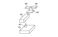
マイクロレンズMLを介して半導体基板15の裏面に光が入射すると、光電変換によってN型半導体領域601に電子が生じる。すなわち、N型半導体領域601は、光電変換装置の感度領域(第1領域)として機能する。この電子(信号電荷)は、N型半導体領域603を介してN型半導体領域602に移動する。すなわち、N型半導体領域602は、光電変換装置の電荷を蓄積する蓄積領域(第2領域)として機能する。N型半導体領域603(第3領域)は、N型半導体領域602からN型半導体領域601への電子の移動経路である。これを実現するため、N型半導体領域602からN型半導体領域601に向かう電子の移動経路上では、電子に対するポテンシャルが単調に増加していることが望ましい。
When light is incident on the back surface of the
図17は、本実施形態に係るフォトダイオードの断面模式図である。図17は、図15及び図16と同様の断面について、電荷を転送するための構造をより詳細に説明する図である。半導体基板15は、フローティングディフュージョンFDを構成する半導体領域605を含む。また、N型半導体領域602と半導体領域605の間のP型半導体領域604に対応する位置には、転送トランジスタM1A、M1Bのゲート電極606が第1面上に配されている。ゲート電極606の電圧を制御することにより、半導体領域602に蓄積された電荷を半導体領域605に転送することができる。なお、図17においては、2つの半導体領域605が別々の領域として図示されているが、図13に示されているように、図17における2つの半導体領域605は、電気的に接続された同電位のノードであり得る。
17 is a schematic cross-sectional view of a photodiode according to this embodiment. FIG. 17 is a diagram illustrating in more detail the structure for transferring charges in a cross section similar to that of FIG. 15 and FIG. 16. The
図18は、本実施形態に係る画素600の平面模式図である。図18は、図13に示した画素600の回路の具体的なレイアウトの一例を示している。図18には、フォトダイオード、トランジスタ等を構成する半導体領域及びマイクロレンズMLの位置が図示されている。また、図18には、転送トランジスタM1A、M1Bのゲート電極606、リセットトランジスタM2のゲート電極607、増幅トランジスタM3のゲート電極608及び選択トランジスタM4のゲート電極609が図示されている。また、図18には、これらの各部を接続する配線WLも図示されている。
Figure 18 is a schematic plan view of a
平面視において、N型半導体領域602と半導体領域605の間には、転送トランジスタM1A、M1Bのゲート電極606が配されている。半導体領域605は配線WLを介してリセットトランジスタM2の主電極を構成する半導体領域610及び増幅トランジスタM3のゲート電極608に接続されている。ゲート電極606、607、609には、配線WLが接続されており、配線WLを介して垂直走査回路103から制御信号が入力される。
In plan view, the
リセットトランジスタM2及び増幅トランジスタM3の主電極を構成する半導体領域611には、電位VDDを有する電源電位線として機能する配線WLが接続されている。選択トランジスタM4の主電極を構成する半導体領域612には、外部に信号電圧を出力するための信号線107として機能する配線WLが接続されている。
A wiring WL that functions as a power supply potential line having a potential VDD is connected to the
本実施形態では、N型半導体領域601とN型半導体領域602とが、N型半導体領域603を介して接続されていればよい。これにより、平面視において、N型半導体領域601とN型半導体領域602を互いに異なる形状とすることができる。また、N型半導体領域601とN型半導体領域602の位置関係は互いに独立に設計可能であるため、N型半導体領域601とN型半導体領域602の位置関係の具体的な態様には種々のものがあり得る。N型半導体領域601とN型半導体領域602の配置例を2種類説明する。
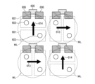
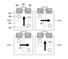
In this embodiment, it is sufficient that the N-
図19(a)、図19(b)及び図19(c)は、本実施形態に係る半導体領域の配置の第1の例を示す模式図である。図19(a)は、N型半導体領域601、602、603、半導体領域605及びゲート電極606の配置を示す斜視模式図である。図19(a)に示されているように、N型半導体領域601とN型半導体領域602とは、いずれも図面奥行方向に延在する直方体状をなしている。すなわち、N型半導体領域601とN型半導体領域602とは、同じ方向に延在している。
Figures 19(a), 19(b), and 19(c) are schematic diagrams showing a first example of the arrangement of semiconductor regions according to this embodiment. Figure 19(a) is a perspective schematic diagram showing the arrangement of N-
図19(b)は、N型半導体領域601、602、603、半導体領域605及びゲート電極606の配置を示す平面模式図である。図19(b)に示されているように、N型半導体領域601とN型半導体領域602とは、いずれも図面縦方向に延在している。言い換えると、2つのN型半導体領域601は、図面横方向に並んで配されており、2つのN型半導体領域602も、図面横方向に並んで配されている。この構成では、光電変換により電荷が生成されるN型半導体領域601が横方向に離れた位置に並んでいることから、横方向の視差を主として検出し得る像面位相差オートフォーカス用の信号を取得することができる。図19(b)には位相差検出の方向が矢印613によって示されている。
19(b) is a schematic plan view showing the arrangement of the N-
図19(c)は、N型半導体領域602の間の分離領域として機能する領域604bとN型半導体領域601の間の分離領域として機能する領域604cとの平面視における位置関係を示す平面模式図である。図19(c)に示されるように、領域604bと領域604cとは、いずれも図面縦方向に延在している。
Figure 19(c) is a schematic plan view showing the positional relationship in a plan view between
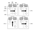
図20(a)、図20(b)及び図20(c)は、本実施形態に係る半導体領域の配置の第2の例を示す模式図である。図19(a)、図19(b)及び図19(c)との主な相違点は半導体領域601の配置である。
20(a), 20(b), and 20(c) are schematic diagrams showing a second example of the arrangement of semiconductor regions according to this embodiment. The main difference from FIGS. 19(a), 19(b), and 19(c) is the arrangement of the
図20(a)に示されているように、N型半導体領域602は、いずれも図面奥行方向に延在する直方体状をなしており、N型半導体領域601は、いずれも図面横方向に延在する直方体状をなしている。すなわち、N型半導体領域601とN型半導体領域602とは、平面視において互いに直交する方向、すなわち、異なる方向に延在している。
As shown in FIG. 20(a), each of the N-
図20(b)に示されているように、N型半導体領域602は、いずれも図面縦方向に延在しており、N型半導体領域601は、いずれも図面横方向に延在している。言い換えると、2つのN型半導体領域601は、図面縦方向に並んで配されており、2つのN型半導体領域602も、図面横方向に並んで配されている。この構成では、光電変換により電荷が生成されるN型半導体領域601が縦方向に離れた位置に並んでいることから、縦方向の視差を主として検出し得る像面位相差オートフォーカス用の信号を取得することができる。図20(b)には位相差検出の方向が矢印614によって示されている。
As shown in FIG. 20(b), both N-
図20(c)は、N型半導体領域602の間の分離領域として機能する領域604bとN型半導体領域601の間の分離領域として機能する領域604cとの平面視における位置関係を示す平面模式図である。図20(c)に示されるように、領域604bは、図面縦方向に在しており、領域604cは、図面横方向に延在している。すなわち、領域604bと領域604cとは、平面視において互いに直交する方向、すなわち、異なる方向に延在している。
Figure 20(c) is a schematic plan view showing the positional relationship in a plan view between
図21(a)及び図21(b)は、画素600の配置例を示す平面模式図である。図21(a)は、図19(a)、図19(b)及び図19(c)に示した第1の例の画素600を行列状に配置した例である。この例では、位相差検出の方向を示す矢印613の向きは横方向となっている。図21(b)は、図20(a)、図20(b)及び図20(c)に示した第2の例の画素600を行列状に配置した例である。この例では、位相差検出の方向を示す矢印614の向きは縦方向となっている。
21(a) and 21(b) are schematic plan views showing an example of the arrangement of
以上述べたように、本実施形態の画素600は、深さD1に配されたN型半導体領域602と、第1面に対して深さD1よりも深い深さD3に配されたN型半導体領域601とを有している。N型半導体領域601の厚さを十分な厚さとすることにより、第2面側から入射された光の大部分は、N型半導体領域601で吸収され、N型半導体領域602までは到達しない。これにより、N型半導体領域601は光電変換により入射光から電荷を生成する感度領域として機能する。N型半導体領域601で生成された電荷は、N型半導体領域603を介してN型半導体領域602に移動し、蓄積される。すなわち、N型半導体領域602は光電変換により生成された電荷を蓄積する蓄積領域として機能する。
As described above, the
このように、N型半導体領域601とN型半導体領域602は基板の厚さ方向の位置が異なることにより、互いに異なる機能を有している。そのため、N型半導体領域601とN型半導体領域602の平面視形状を目的に応じて異なる形状に設計することができる。別の観点では、N型半導体領域602の間の分離領域として機能する領域604bとN型半導体領域601の間の分離領域として機能する領域604cとを平面視において異なる形状に設計することができる。
In this way, the N-
図19(b)、図21(a)の第1の例では、2つのN型半導体領域601が図面横方向に並んで配されており、横方向の視差を主として検出し得る像面位相差オートフォーカス用の信号を取得することができる。このような設計は、被写体が縦方向のストライプ模様に近いものである場合により有効である。これに対し、図20(b)、図21(b)の第2の例では、2つのN型半導体領域601が図面縦方向に並んで配されており、縦方向の視差を主として検出し得る像面相差オートフォーカス用の信号を取得することができる。このような設計は、被写体が横方向のストライプ模様に近いものである場合により有効である。このように、想定される被写体の特徴を考慮して、感度領域として機能するN型半導体領域601の形状を変えることにより、像面位相差オートフォーカスの検出方向を異ならせることができる。この2つの例では、蓄積領域として機能するN型半導体領域602の設計は同一である。また、ゲート電極606、半導体領域605、配線WL等も2つの例において設計を同一とすることができる。すなわち、感度領域以外の部分の設計は蓄積領域の形状に依存せずに共通化することができるため、設計が簡略化される。
In the first example of FIG. 19(b) and FIG. 21(a), two N-
以上のように本実施形態によれば、像面位相差オートフォーカス用の信号を出力するフォトダイオードの構造を基板の厚さ方向の位置を考慮して適正化し得る光電変換装置が提供される。これにより、被写体の形状に応じて適正な視差検出方向の信号を出力し得る光電変換装置が提供される。 As described above, according to this embodiment, a photoelectric conversion device is provided that can optimize the structure of the photodiode that outputs a signal for image plane phase difference autofocusing by taking into account the position in the thickness direction of the substrate. This provides a photoelectric conversion device that can output a signal with an appropriate parallax detection direction according to the shape of the subject.
なお、本実施形態のように通常のフォトダイオードを用いる回路構成であっても第4実施形態と同様にフォトダイオードが配された第1基板と信号処理回路が配された第2基板が積層された構造を適用することができる。この場合、フォトダイオードの感度領域の面積を広くすることができ、感度がより向上される。 Even in a circuit configuration using a normal photodiode as in this embodiment, a structure in which a first substrate on which a photodiode is arranged and a second substrate on which a signal processing circuit is arranged are stacked as in the fourth embodiment can be applied. In this case, the area of the sensitive region of the photodiode can be increased, further improving sensitivity.
[第6実施形態]
第6実施形態に係る光電変換装置について説明する。本実施形態の説明において、第1実施形態乃至第5実施形態と同様の機能を有する部分には同様の符号を付し、詳細な説明を省略又は簡略化することもある。本実施形態の光電変換装置は、第5実施形態で述べた画素600の配列の変形例である。
Sixth Embodiment
A photoelectric conversion device according to the sixth embodiment will be described. In the description of this embodiment, parts having the same functions as those in the first to fifth embodiments are given the same reference numerals, and detailed description may be omitted or simplified. The photoelectric conversion device according to this embodiment is a modified example of the arrangement of the
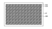
図22は、本実施形態に係る画素の平面模式図である。図22には、2行×2列の4画素が図示されており、N型半導体領域601、603、半導体領域605、ゲート電極606及びマイクロレンズMLの配置が示されている。N型半導体領域602の配置は図19(b)及び図20(b)と同様であるため、図22では、図示が省略されている。
Figure 22 is a schematic plan view of a pixel according to this embodiment. Four pixels of 2 rows and 2 columns are shown in Figure 22, and the arrangement of N-
図22における左上の画素においては、図20(b)と同様に2つのN型半導体領域601(第1のマイクロレンズMLに対応する第1のフォトダイオード群)は、図面縦方向に並んで配されている。図22における左上の画素に隣接する画素(右上の画素及び左下の画素)においては、図19(b)と同様に2つのN型半導体領域601(第2のマイクロレンズMLに対応する第2のフォトダイオード群)は、図面横方向に並んで配されている。 In the upper left pixel in FIG. 22, two N-type semiconductor regions 601 (first photodiode group corresponding to the first microlens ML) are arranged side by side in the vertical direction of the drawing, similar to FIG. 20(b). In the pixels adjacent to the upper left pixel in FIG. 22 (the upper right pixel and the lower left pixel), two N-type semiconductor regions 601 (second photodiode group corresponding to the second microlens ML) are arranged side by side in the horizontal direction of the drawing, similar to FIG. 19(b).
図23は、画素600の配置例を示す平面模式図である。図23は、図22に示した2行×2列の4画素を一単位として繰り返し配置した例である。この例では、位相差検出の方向を示す矢印613、614の向きは横方向と縦方向が交互に繰り返されている。
Fig. 23 is a schematic plan view showing an example of the arrangement of
本実施形態においては、画素部61に図19(b)の第1の例で示した横方向の視差を主として検出し得る画素と、図20(b)の第2の例で示した縦方向の視差を主として検出し得る画素との両方が含まれている。したがって、検出方向が異なる複数組の像面位相差オートフォーカス用信号を得ることができる。これにより、画素部61の複数の画素600から被写体の形状への依存性が小さく、かつ高精度な焦点検出が可能となる。例えば被写体がストライプ模様である場合には、ストライプの方向によらずに安定した焦点検出の精度を得ることができる。以上のように本実施形態では、様々なシチュエーションに対応した焦点検出を実現し得る光電変換装置が提供される。
In this embodiment, the
なお、上述の例では、位相差検出の方向を示す矢印613、614の向きの組み合わせは横方向と縦方向の2種類のみであるが、これ以外の方向の2種類の組み合せであってもよく、3種類以上の組み合わせであってもよい。図24は、本実施形態の変形例に係る画素の平面模式図である。図24に示されているように、2つのN型半導体領域601を斜め方向に並ぶ三角形形状とすることにより、矢印615により示されている位相差検出の方向を斜め方向とすることができる。画素部61に図24の構成の画素600を含ませることにより、更に多様な検出方向の像面位相差オートフォーカス用信号を得ることができる。
In the above example, the combination of the directions of the
[第7実施形態]
第7実施形態に係る光電変換装置について説明する。本実施形態の説明において、第1実施形態乃至第6実施形態と同様の機能を有する部分には同様の符号を付し、詳細な説明を省略又は簡略化することもある。本実施形態の光電変換装置は、第5実施形態及び第6実施形態で述べた画素600の配列の変形例である。
[Seventh embodiment]
A photoelectric conversion device according to the seventh embodiment will be described. In the description of this embodiment, parts having the same functions as those of the first to sixth embodiments are given the same reference numerals, and detailed description may be omitted or simplified. The photoelectric conversion device according to this embodiment is a modified example of the arrangement of the
図25は、本実施形態に係る画素の平面模式図である。図25には、図22と同様に2行×2列の4画素が図示されており、N型半導体領域601、603、半導体領域605及びゲート電極606の配置が示されている。なお、マイクロレンズMLについては図示が省略されている。更に、図25には、各画素に対応して設けられたカラーフィルタCFR、CFG、CFBの配置が示されている。カラーフィルタCFR、CFG、CFBは図10と同様に、半導体基板の第2面とマイクロレンズMLの間に設けられている。
Figure 25 is a schematic plan view of a pixel according to this embodiment. As in Figure 22, Figure 25 illustrates four pixels in two rows and two columns, and shows the arrangement of N-
カラーフィルタCFRは、赤色の光を透過させるカラーフィルタであり、2行×2列の4画素内に1つ設けられている。カラーフィルタCFGは、緑色の光を透過させるカラーフィルタであり、2行×2列の4画素内に2つ設けられている。カラーフィルタCFBは、青色の光を透過させるカラーフィルタであり、2行×2列の4画素内に1つ設けられている。図25のカラーフィルタCFR、CFG、CFBの配列方法は、ベイヤー配列と呼ばれているものであるがこれは一例であり、別の配列方法であってもよい。以下では、カラーフィルタCFR、CFG、CFBが設けられている画素をそれぞれ赤色画素、緑色画素、青色画素と呼ぶこともある。 The color filter CFR is a color filter that transmits red light, and one filter is provided for every four pixels of two rows and two columns. The color filter CFG is a color filter that transmits green light, and two filters are provided for every four pixels of two rows and two columns. The color filter CFB is a color filter that transmits blue light, and one filter is provided for every four pixels of two rows and two columns. The arrangement method of the color filters CFR, CFG, and CFB in FIG. 25 is called a Bayer arrangement, but this is only one example, and other arrangement methods may be used. Below, the pixels in which the color filters CFR, CFG, and CFB are provided may also be called red pixels, green pixels, and blue pixels, respectively.
図25に示されているように、本実施形態においては、図19(b)の第1の例で示した横方向の視差を主として検出し得る画素が緑色画素であり、図20(b)の第2の例で示した縦方向の視差を主として検出し得る画素が赤色画素又は青色画素である。このように、本実施形態では、検出方向が異なる画素が異なる色のカラーフィルタを有している。 As shown in FIG. 25, in this embodiment, the pixels capable of primarily detecting horizontal parallax as shown in the first example of FIG. 19(b) are green pixels, and the pixels capable of primarily detecting vertical parallax as shown in the second example of FIG. 20(b) are red pixels or blue pixels. In this way, in this embodiment, pixels with different detection directions have color filters of different colors.
像面位相差オートフォーカスのための信号の比較においては色が混在していない方が精度良く焦点の検出ができるため、検出方向ごとに色が揃っていることが望ましい。そこで、本実施形態では、検出方向が異なる画素が異なる色のカラーフィルタを有するようにカラーフィルタの配列が設定されている。これにより、本実施形態によれば、カラーの撮像に対応した光電変換装置であっても高精度な焦点検出が可能となる。 When comparing signals for image plane phase detection autofocus, it is preferable that colors are not mixed in order to detect focus with greater accuracy. Therefore, in this embodiment, the color filters are arranged so that pixels with different detection directions have color filters of different colors. As a result, this embodiment enables highly accurate focus detection even in a photoelectric conversion device that supports color imaging.
なお、図25の構成では、赤色画素、緑色画素及び青色画素から出力された信号はいずれも像面位相差オートフォーカスに用いることができるが、これらのすべてを用いてもよく、これらの1つ又は2つを用いてもよい。シリコンの基板の光吸収率は、赤色又は青色に比べて緑色の方が高いため、緑色画素は、他の画素に比べて高感度である。そのため、少なくとも緑色画素から出力された信号は、像面位相差オートフォーカスに用いられることが望ましい。 In the configuration of FIG. 25, the signals output from the red, green, and blue pixels can all be used for image plane phase difference autofocus, but all of them, or one or two of them, may be used. The light absorption rate of the silicon substrate is higher for green than for red or blue, so the green pixels are more sensitive than the other pixels. Therefore, it is desirable to use at least the signals output from the green pixels for image plane phase difference autofocus.
図25のカラーフィルタとN型半導体領域601の配列の対応関係は一例であり、これ以外のものであってもよい。図26は、本実施形態の変形例に係る画素の平面模式図である。図26の変形例は、N型半導体領域601の配列が図25と異なっている。具体的には、2つの緑色画素の一方が図19(b)の第1の例で示した横方向の視差を主として検出し得る画素であり、他方が図20(b)の第2の例で示した縦方向の視差を主として検出し得る画素である。この構成では、高感度な緑色画素から出力された信号を2つの検出方向の焦点検出に用いることができる。なお、赤色画素及び青色画素の一方又は両方から出力された信号を更に焦点検出に用いてもよい。
The correspondence between the color filters and the arrangement of the N-
[第8実施形態]
第8実施形態に係る光電変換装置について説明する。本実施形態の説明において、第1実施形態乃至第7実施形態と同様の機能を有する部分には同様の符号を付し、詳細な説明を省略又は簡略化することもある。本実施形態の光電変換装置は、第5実施形態で述べた画素600のフォトダイオードとしてアバランシェダイオードに変形した例である。アバランシェダイオードの詳細な構造、アバランシェ増倍の動作等は第1実施形態で述べたものと同様である。
[Eighth embodiment]
A photoelectric conversion device according to an eighth embodiment will be described. In the description of this embodiment, parts having the same functions as those of the first to seventh embodiments are given the same reference numerals, and detailed description may be omitted or simplified. The photoelectric conversion device according to this embodiment is an example in which the photodiode of the
図27は、本実施形態に係るアバランシェダイオードの断面模式図である。本実施形態の半導体基板15は、N型半導体領域601、602から電荷を収集する領域として機能し、かつ、信号を取得する端子としても機能する半導体領域616を有する。半導体領域616は、第1実施形態の第1半導体領域71に相当する部分である。また、本実施形態の画素600の断面構造には、第5実施形態乃至第7実施形態の電荷転送の機能を有するゲート電極606及びフローティングディフュージョンFDを構成する半導体領域605が設けられていない。
Figure 27 is a schematic cross-sectional view of the avalanche diode according to this embodiment. The
図28(a)及び図28(b)は、N型半導体領域601、602、603及び半導体領域616の配置を示す平面模式図である。図28(a)は、図19(a)で述べた第1の例に対応する配置例である。図28(a)の構成では、図19(a)の構成と同様に、横方向の視差を主として検出し得る像面位相差オートフォーカス用の信号を取得することができる。また、図28(b)は、図20(a)で述べた第2の例に対応する配置例である。図28(b)の構成では、図20(a)の構成と同様に、奥行き方向の視差を主として検出し得る像面位相差オートフォーカス用の信号を取得することができる。
28(a) and 28(b) are schematic plan views showing the arrangement of N-
したがって、本実施形態のようにフォトダイオードがアバランシェ増倍の動作を行うアバランシェダイオードである場合であっても第5乃至第7実施形態と同様の構造が実現可能である。すなわち、アバランシェダイオードの構造を基板の厚さ方向の位置を考慮して適正化し得る光電変換装置が提供される。 Therefore, even if the photodiode is an avalanche diode that performs avalanche multiplication as in this embodiment, a structure similar to that of the fifth to seventh embodiments can be realized. In other words, a photoelectric conversion device is provided in which the structure of the avalanche diode can be optimized by taking into account its position in the thickness direction of the substrate.
[第9実施形態]
第9実施形態に係る光電変換装置について説明する。本実施形態の説明において、第1実施形態乃至第8実施形態と同様の機能を有する部分には同様の符号を付し、詳細な説明を省略又は簡略化することもある。本実施形態の光電変換装置は、第5実施形態で述べた画素600において、画素間の素子分離領域としてDTI(Deep Trench Isolation)が用いられている例である。
[Ninth embodiment]
A photoelectric conversion device according to the ninth embodiment will be described. In the description of this embodiment, parts having the same functions as those of the first to eighth embodiments are given the same reference numerals, and detailed description may be omitted or simplified. The photoelectric conversion device according to this embodiment is an example in which DTI (Deep Trench Isolation) is used as an element isolation region between pixels in the
図29は、本実施形態に係るフォトダイオードの平面模式図であり、図30は、本実施形態に係るフォトダイオードの断面模式図である。図29及び図30のフォトダイオードは、DTI617が追加されている点が第5実施形態の図14、図15等と相違する。図29に示されているように、DTI617は、平面視において2つのN型半導体領域601を囲うように、格子状に配されている。また、図30に示されているように、DTI617は、N型半導体領域601、602の側部に配されている。
Figure 29 is a schematic plan view of a photodiode according to this embodiment, and Figure 30 is a schematic cross-sectional view of the photodiode according to this embodiment. The photodiodes in Figures 29 and 30 differ from those in Figures 14 and 15 of the fifth embodiment in that a
入射光によりN型半導体領域601で電子が生成されると、P型半導体領域604のポテンシャル障壁を越えて隣接画素に電子が移動することによるクロストークが生じる場合がある。このクロストークは、カラー撮像が可能な画素構成の場合には混色の原因ともなり得る。また、第2面からの入射光がN型半導体領域602に到達しにくいようにN型半導体領域601が厚い場合にはこのクロストークが顕著になり得る。そこで、本実施形態では、隣接画素への電子の移動経路であるN型半導体領域601、602の側部に絶縁性が良好なDTI617が配されていることにより、クロストークの影響が低減される。DTI617は、少なくとも電子が生成されるN型半導体領域601の側部に配されるように、N型半導体領域601と同程度の深さに至るように形成されていることが望ましい。
When electrons are generated in the N-
[第10実施形態]
第10実施形態に係る光電変換装置について説明する。本実施形態の説明において、第1実施形態乃至第9実施形態と同様の機能を有する部分には同様の符号を付し、詳細な説明を省略又は簡略化することもある。本実施形態の光電変換装置は、第5実施形態で述べた画素600において、1つのマイクロレンズMLに対応するフォトダイオードの個数を1個に削減したものである。
[Tenth embodiment]
A photoelectric conversion device according to a tenth embodiment will be described. In the description of this embodiment, parts having the same functions as those of the first to ninth embodiments are given the same reference numerals, and detailed description may be omitted or simplified. In the photoelectric conversion device of this embodiment, the number of photodiodes corresponding to one microlens ML in the
図31は、本実施形態に係るフォトダイオードの平面模式図である。図32は、本実施形態に係るフォトダイオードの断面模式図である。図33は、本実施形態に係るフォトダイオードの斜視模式図である。図34は、本実施形態に係る画素の平面模式図である。図31乃至図34の画素600には、N型半導体領域602(第3のマイクロレンズMLに対応する第3のフォトダイオード群)が1つのみ設けられている。また、マイクロレンズMLの概ね全体をカバーするようにN型半導体領域601の形状が変形されている。本実施形態では、これらの点が第5実施形態の図14、図15等と相違する。
Figure 31 is a schematic plan view of a photodiode according to this embodiment. Figure 32 is a schematic cross-sectional view of a photodiode according to this embodiment. Figure 33 is a schematic perspective view of a photodiode according to this embodiment. Figure 34 is a schematic plan view of a pixel according to this embodiment. The
図31及び図32に示されているように、画素600には、1つのN型半導体領域602が、左側に1つのみ配されている。また、図31及び図32に示されているように、N型半導体領域601は、マイクロレンズMLの概ね全体をカバーするように配されている。図33及び図34に示されているように、N型半導体領域602が1つであるため、N型半導体領域603も1つのみ配されている。ゲート電極606の個数も1つのみであってもよいが、図33及び図34に示されているように、配置の対称性を維持するため、図18と同様にゲート電極606が2つ配されていてもよい。
31 and 32, the
本実施形態の画素600は、像面位相差オートフォーカス用の信号の取得ではなく、撮像用の信号の取得に用いられる。本実施形態の1つのN型半導体領域601は、第5実施形態のそれと比べて概ね2倍の面積を有しており、2倍の電子が生成され得る。したがって、出力される1つの信号の感度が概ね2倍となる。また、読み出し時に駆動させる必要があるゲート電極606の個数は1個であるため、読み出しが高速化する。
The
以上のように本実施形態によれば、高速かつ高感度に撮像を行うことができる光電変換装置が提供される。本実施形態の画素600は、高速かつ高感度な撮像が要求される電子ビューファインダ等の用途に有効である。図12の画素部61に含まれる複数の画素600のうちの一部を本実施形態の画素600とすることで、電子ビューファインダ用の間引き画像を高速かつ高感度に取得することができる。
As described above, according to this embodiment, a photoelectric conversion device capable of capturing images at high speed and high sensitivity is provided. The
[第11実施形態]
第11実施形態に係る光電変換装置について説明する。本実施形態の説明において、第1実施形態乃至第10実施形態と同様の機能を有する部分には同様の符号を付し、詳細な説明を省略又は簡略化することもある。本実施形態の光電変換装置は、第5実施形態で述べた画素600において、2つのN型半導体領域601の形状を異ならせたものである。
[Eleventh embodiment]
A photoelectric conversion device according to an eleventh embodiment will be described. In the description of this embodiment, parts having the same functions as those of the first to tenth embodiments are given the same reference numerals, and detailed description may be omitted or simplified. In the photoelectric conversion device of this embodiment, the shape of the two N-
図35は、本実施形態に係る半導体領域の配置を示す平面模式図である。図36は、本実施形態に係るフォトダイオードの断面模式図である。図37は、本実施形態に係るフォトダイオードの斜視模式図である。図35乃至図37の画素600においては、2つのN型半導体領域601が互いに異なる形状及び面積を有している点が第5実施形態の図15、図19等と相違する。
Figure 35 is a schematic plan view showing the arrangement of semiconductor regions according to this embodiment. Figure 36 is a schematic cross-sectional view of a photodiode according to this embodiment. Figure 37 is a schematic perspective view of a photodiode according to this embodiment. The
図35及び図36に示されているように、2つのN型半導体領域601の平面視及び断面視における形状及び面積は互いに異なっている。また、図37に示されているように、2つのN型半導体領域601の形状及び体積は互いに異なっている。
As shown in Figures 35 and 36, the shapes and areas of the two N-
画素部61の中心から離れた位置の画素600には、カメラ等の撮像システムの光学系を通過した光が撮像面に対して斜めに入射する。この入射光の角度は像面位相差オートフォーカスの精度に影響を与えるため、これを低減するためにマイクロレンズMLの光軸を画素600の中心からずらして配置する手法が知られている。このとき、マイクロレンズMLの光軸のずれを考慮して感度領域であるN型半導体領域601の位置も中心からずらして異なる形状とすることが望ましい。この配置では、平面視における2つのN型半導体領域601の面積が互いに異なるものとなる。
At
本実施形態では、2つのN型半導体領域601を互いに異なる形状とすることができるため、画素部61内の座標又はマイクロレンズMLの位置を考慮して2つのN型半導体領域601の形状を適切に設計することができる。これにより、像面位相差オートフォーカスの精度が画素部61内の広範囲にわたって向上する。あるいは、画素部61内の像面位相差オートフォーカスが可能な範囲が拡大する。なお、画素600への入射光の角度は、画素部61内の座標(像高)に依存して滑らかに変わるため、これを考慮して、N型半導体領域601の形状も画素部61内の座標(像高)に応じて滑らかに変えることが望ましい。
In this embodiment, the two N-
以上のように、本実施形態によれば、2つのN型半導体領域601の形状を異ならせることにより、像面位相差オートフォーカスの精度が向上された光電変換装置が提供される。
As described above, according to this embodiment, by making the shapes of the two N-
[第12実施形態]
第12実施形態に係る光電変換装置について説明する。本実施形態の説明において、第1実施形態乃至第11実施形態と同様の機能を有する部分には同様の符号を付し、詳細な説明を省略又は簡略化することもある。本実施形態においては、第5実施形態乃至第7実施形態で述べた画素600の配列方法を様々に変更させた変形例を説明する。
[Twelfth embodiment]
A photoelectric conversion device according to the twelfth embodiment will be described. In the description of this embodiment, parts having the same functions as those of the first to eleventh embodiments will be given the same reference numerals, and detailed description may be omitted or simplified. In this embodiment, a modified example in which the arrangement method of the
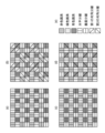
図38(a)、図38(b)、図38(c)、図38(d)及び図38(e)は、本実施形態に係る画素の配置例を示す平面模式図である。図38(e)は、図38(a)、図38(b)、図38(c)及び図38(d)の凡例を示している。 Figures 38(a), 38(b), 38(c), 38(d), and 38(e) are schematic plan views showing examples of pixel arrangements according to this embodiment. Figure 38(e) shows the legends for Figures 38(a), 38(b), 38(c), and 38(d).
具体的には、図38(a)、図38(b)、図38(c)及び図38(d)において、画素600を示す正方形の枠内のパターンは、画素600が赤色画素、緑色画素、青色画素のいずれであるかを示している。言い換えると当該パターンは、画素600に設けられているカラーフィルタCFR、CFG、CFBの色を示している。図38(a)、図38(b)、図38(c)及び図38(d)に示されているように、これらの画素600の色の配列は、2行×2列の4画素を一単位として同じ配列が繰り返されるベイヤー配列をなしている。
Specifically, in Figures 38(a), 38(b), 38(c), and 38(d), the pattern within the square
画素600を示す正方形の枠内のパターン内に付されている線分の向きは、P型半導体領域604のうちの2つのN型半導体領域601を分離している領域604cの向きを示している。言い換えると、正方形を当該線分により分割することにより得られる2つの図形の形状が、2つのN型半導体領域601の形状を模式的に示している。図38(e)に記載されているように、2つのN型半導体領域601が横方向に並んでいる分離方式を水平分離と呼ぶ。2つのN型半導体領域601が縦方向に並んでいる分離方式を垂直分離と呼ぶ。2つのN型半導体領域601が左下及び右上に並んでいる分離方式を第1の対角分離と呼ぶ。2つのN型半導体領域601が左上及び右下に並んでいる分離方式を第2の対角分離と呼ぶ。これらの分離方向は、像面位相差オートフォーカスの位相差検出方向に対応する。
The direction of the line segment in the pattern within the square frame showing the
図38(a)の例では、1行目及び2行目の画素600が水平分離であり、3行目及び4行目の画素600が垂直分離である。5行目から8行目も同様の配列となっている。このように、図38(a)の例では2行の水平分離と2行の垂直分離を含む4行を一単位として4行ごとに同じ配列が繰り返されている。
In the example of FIG. 38(a), the
図38(b)の例では、1行目及び2行目の画素600が水平分離と第1の対角分離の繰り返し配列であり、3行目及び4行目の画素600が第2の対角分離と垂直分離の繰り返し配列である。5行目から8行目も同様の配列となっている。このように、図38(b)の例では水平分離、垂直分離、第1の対角分離及び第2の対角分離を含む4行×4列を一単位として同じ配列が繰り返されている。
In the example of FIG. 38(b), the
図38(c)の例では、1行目の画素600が水平分離であり、2行目の画素600が垂直分離である。3行目以降もこれらが繰り返される配列となっている。このように、図38(c)の例では1行の水平分離と1行の垂直分離を含む2行を一単位として2行ごとに同じ配列が繰り返されている。この配列では、赤色画素と赤色画素の横の緑色画素が水平分離であり、青色画素と青色画素の横の緑色画素が垂直分離である。このように、一部の色の画素が一定の分離方向になるように、画素の色と分離方向が対応付けられている構成であってもよい。
In the example of FIG. 38(c), the
図38(d)の例では、1行目の赤色画素が水平分離であり、1行目の緑色画素が垂直分離である。また、2行目の緑色画素が垂直分離であり、2行目の青色画素が第1の対角分離又は第2の対角分離の繰り返し配列である。3行目以降もこれらが繰り返される配列となっている。このように、図38(d)の例では水平分離、垂直分離、第1の対角分離及び第2の対角分離を含む2行×4列を一単位として同じ配列が繰り返されている。この配列では、赤色画素と青色画素の横の緑色画素が水平分離であり、赤色画素の横の緑色画素が垂直分離である。青色画素は、第1の対角分離又は第2の対角分離である。このように、一部の色の画素が一定の分離方向になるように、画素の色と分離方向が対応付けられている構成であってもよい。 In the example of FIG. 38(d), the red pixels in the first row are horizontally separated, and the green pixels in the first row are vertically separated. The green pixels in the second row are vertically separated, and the blue pixels in the second row are a repeating arrangement of the first diagonal separation or the second diagonal separation. These are repeated from the third row onwards. In this way, in the example of FIG. 38(d), the same arrangement is repeated in a unit of 2 rows x 4 columns including horizontal separation, vertical separation, first diagonal separation, and second diagonal separation. In this arrangement, the green pixels next to the red and blue pixels are horizontally separated, and the green pixels next to the red pixels are vertically separated. The blue pixels are first diagonally separated or second diagonally separated. In this way, the pixel colors and the separation directions may be associated so that some pixels of a certain color are separated in a certain direction.
以上のように、本実施形態では、画素部61に種々の分離方向の画素600を含ませることにより、多様な検出方向の像面位相差オートフォーカス用信号を得ることができる。
As described above, in this embodiment, by including
なお、図38(a)から図38(e)の例における画素600の色は、赤色、緑色、青色以外の色であってもよい。例えば、画素600の色は、補色であるシアン、マゼンタ、イエローであってもよく、白色であってもよい。また、画素600は、赤外線を透過し、可視光を遮断する赤外線フィルタを有する赤外線画素であってもよい。
The color of
また、画素600の配列は、ベイヤー配列に限定されるものではなく、他の配列であってもよい。例えば、赤色画素、緑色画素、青色画素を同じ行又は同じ列に並べる配列であってもよく、六角形の画素を配列するヘキサゴナル配列であってもよく、ベイヤー配列等の四角形を一単位とする画素群を半ピッチずつずらして配列する千鳥配列であってもよい。また、一部の画素600が第11実施形態のフォトダイオードの個数が1個の画素600に置き換えられていてもよい。
The arrangement of the
[第13実施形態]
第13実施形態に係る撮像システムについて説明する。本実施形態の撮像システムは、第1実施形態乃至第12実施形態のいずれかの光電変換装置を有する。撮像システムとは、デジタルスチルカメラ、デジタルビデオカメラ、携帯電話用デジタルカメラ等の静止画又は動画の撮影に用いられる装置である。
[Thirteenth embodiment]
An imaging system according to the thirteenth embodiment will be described. The imaging system according to the present embodiment includes a photoelectric conversion device according to any one of the first to twelfth embodiments. The imaging system is a device used for capturing still or moving images, such as a digital still camera, a digital video camera, or a digital camera for a mobile phone.
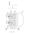
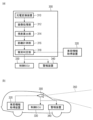
図39は、第13実施形態に係る撮像システムのブロック図である。撮像システムは、レンズ部1001、レンズ駆動装置1002、シャッタ1003、シャッタ駆動装置1004、光電変換装置1005、撮像信号処理回路1006及びタイミング発生部1007を有する。撮像システムは、更に、メモリ部1008、全体制御・演算部1009、記録媒体制御I/F(Interface)部1010、記録媒体1011、外部I/F部1012及び測光装置1013を有する。
Figure 39 is a block diagram of an imaging system according to the thirteenth embodiment. The imaging system has a
レンズ部1001は、被写体の光学像を光電変換装置1005に結像させる部分である。レンズ駆動装置1002は、レンズ部1001を駆動する装置である。レンズ駆動装置1002は、レンズ部1001を駆動することにより、ズーム制御、フォーカス制御、絞り制御等を行う。シャッタ1003は、入射光の遮蔽を行う光学部材であり、例えば、メカニカルシャッタが用いられ得る。また、シャッタ1003は、絞りの機能を兼ねていてもよい。シャッタ駆動装置1004は、シャッタ1003の開閉等の制御を行う。
The
光電変換装置1005は、第1実施形態乃至第12実施形態のいずれかの光電変換装置であり、レンズ部1001によって結像された被写体の光学像を画像信号に変換して取得する。撮像信号処理回路1006は、光電変換装置1005から出力される画像信号に対して各種の補正、データ圧縮等を行う回路である。タイミング発生部1007は、光電変換装置1005、撮像信号処理回路1006に、各種タイミング信号を出力する回路である。
The
全体制御・演算部1009は、各種演算と撮像システム全体の制御を行う制御回路である。メモリ部1008は、撮像信号処理回路1006から出力される画像データを一時的に記録するための記録装置である。記録媒体制御I/F部1010は、記録媒体1011に対して記録又は読み出しを行うためのインターフェースである。記録媒体1011は、半導体メモリ等の着脱可能な記録媒体であり、画像データの記録又は読み出しに用いられる。外部I/F部1012は、各種情報、撮影画像等を外部に提供するためのインターフェースであり、コンピュータ等の他の情報処理装置との通信インターフェースであってもよく、表示装置等のユーザインターフェースであってもよい。
The overall control/
次に、撮像システムが測距機能を備えたデジタルスチルカメラである場合の撮影時の動作について説明する。撮像システムのメイン電源がオンになると、撮像システムの制御用の電源と撮像信号処理回路1006等に電力を供給する撮像用の電源が順次オンになる。
Next, we will explain the operation during shooting when the imaging system is a digital still camera equipped with a distance measurement function. When the main power supply of the imaging system is turned on, the power supply for controlling the imaging system and the power supply for imaging that supplies power to the imaging
ユーザが、不図示のレリーズボタンを押下すると、光電変換装置1005は、画像信号を取得し、全体制御・演算部1009は、画像信号のデータに基づいて測距演算を行い、その結果に基づいて被写体までの距離を算出する。その後、レンズ駆動装置1002は、算出された距離に基づいてレンズ部1001を駆動して合焦しているか否かを判断し、合焦していない場合には、再びレンズ部1001を駆動するという処理により焦点調節を行う。測距演算は、光電変換装置1005により取得された画像信号を用いるもの以外に、不図示の測距専用装置で行われるものであってもよい。
When the user presses a release button (not shown), the
合焦が確認されると、撮像システムは、撮影動作を開始する。撮影動作の終了後、光電変換装置1005から出力された画像信号は、撮像信号処理回路1006において処理され、全体制御・演算部1009の制御によりメモリ部1008に書き込まれる。撮像信号処理回路1006は、データの並べ替え、加算等を行う。メモリ部1008に記録されたデータは、全体制御・演算部1009の制御により記録媒体制御I/F部1010を介して記録媒体1011に記録される。また、このデータは、外部I/F部1012を介してコンピュータ等に入力されてもよい。コンピュータは、撮像システムから出力されたデータに対して画像の加工等の処理を行うことができる。
When focus is confirmed, the imaging system starts the imaging operation. After the imaging operation is completed, the image signal output from the
本実施形態の撮像システムは、第1乃至第12実施形態の光電変換装置を備えている。これにより、本実施形態によれば、より高品質な撮像システムが提供される。 The imaging system of this embodiment is equipped with the photoelectric conversion device of the first to twelfth embodiments. As a result, this embodiment provides a higher quality imaging system.
[第14実施形態]
第14実施形態に係る撮像システム及び移動体について説明する。図40(a)及び図40(b)は、本実施形態に係る撮像システム300及び移動体の構成を示す図である。
[Fourteenth embodiment]
An image capturing system and a moving object according to the fourteenth embodiment will be described below. Figures 40(a) and 40(b) are diagrams showing the configurations of an
図40(a)は、車載カメラに関する撮像システム300の一例を示したものである。撮像システム300は、光電変換装置310を有する。本実施形態の光電変換装置310は、上述の第1乃至第12実施形態のいずれかに記載の光電変換装置である。撮像システム300は、光電変換装置310により取得された複数の画像データに対し、画像処理を行う画像処理部312と、光電変換装置310により取得された複数の画像データから視差(視差画像の位相差)の算出を行う視差算出部314を有する。また、撮像システム300は、算出された視差に基づいて対象物までの距離を算出する距離計測部316と、算出された距離に基づいて衝突可能性があるか否かを判定する衝突判定部318と、を有する。ここで、視差算出部314及び距離計測部316は、対象物までの距離情報を取得する距離情報取得手段の一例である。すなわち、距離情報とは、視差、デフォーカス量、対象物までの距離等に関する情報である。衝突判定部318はこれらの距離情報のいずれかを用いて、衝突可能性を判定してもよい。距離情報取得手段は、専用に設計されたハードウェアによって実現されてもよいし、ソフトウェアモジュールによって実現されてもよい。また、FPGA(Field Programmable Gate Array)やASIC(Application Specific Integrated Circuit)等によって実現されてもよいし、これらの組合せによって実現されてもよい。
Figure 40 (a) shows an example of an
撮像システム300は、車両情報取得装置320と接続されており、車速、ヨーレート、舵角等の車両情報を取得することができる。また、撮像システム300は、衝突判定部318での判定結果に基づいて、車両に対して制動力を発生させる制御信号を出力する制御装置である制御ECU330が接続されている。また、撮像システム300は、衝突判定部318での判定結果に基づいて、ドライバーへ警報を発する警報装置340とも接続されている。例えば、衝突判定部318の判定結果として衝突可能性が高い場合、制御ECU330はブレーキをかける、アクセルを戻す、エンジン出力を抑制するなどして衝突を回避、被害を軽減する車両制御を行う。警報装置340は音等の警報を鳴らす、カーナビゲーションシステムなどの画面に警報情報を表示する、シートベルトやステアリングに振動を与えるなどしてユーザに警告を行う。
The
本実施形態では、車両の周囲、例えば前方又は後方を撮像システム300で撮像する。図40(b)に、車両前方(撮像範囲350)を撮像する場合の撮像システム300の配置例を示した。車両情報取得装置320は、撮像システム300又は光電変換装置310に指示を送る。このような構成により、測距の精度をより向上させることができる。
In this embodiment, the surroundings of the vehicle, for example the front or rear, are imaged by the
他の車両と衝突しないように制御する例を説明したが、他の車両に追従して自動運転する制御や、車線からはみ出さないように自動運転する制御などにも適用可能である。更に、撮像システム300は、自車両等の車両に限らず、例えば、船舶、航空機あるいは産業用ロボットなどの移動体(移動装置)に適用することができる。加えて、移動体に限らず、高度道路交通システム(ITS)等、広く物体認識を利用する機器に適用することができる。
Although an example of control to avoid collision with other vehicles has been described, the system can also be applied to control of automatic driving to follow other vehicles, and control of automatic driving to avoid going outside of a lane. Furthermore, the
[変形実施形態]
本発明は、上述の実施形態に限らず種々の変形が可能である。例えば、いずれかの実施形態の一部の構成を他の実施形態に追加した例や、他の実施形態の一部の構成と置換した例も、本発明の実施形態である。
[Modified embodiment]
The present invention is not limited to the above-described embodiments, and various modifications are possible. For example, an example in which a part of the configuration of any of the embodiments is added to another embodiment, or an example in which a part of the configuration of another embodiment is replaced with another embodiment is also an embodiment of the present invention.
また、第13及び第14実施形態に示した装置又はシステムは、本発明の光電変換装置を適用し得る装置又はシステムの構成例を示したものである。そのため、本発明の光電変換装置を適用可能な装置又はシステムは図39、図40(a)又は図40(b)に示した構成に限定されない。 The devices or systems shown in the thirteenth and fourteenth embodiments are configuration examples of devices or systems to which the photoelectric conversion device of the present invention can be applied. Therefore, devices or systems to which the photoelectric conversion device of the present invention can be applied are not limited to the configurations shown in Figures 39, 40(a) and 40(b).
また、第1乃至第12実施形態に示した半導体領域の導電型は変更可能であり、例えば、すべての導電型が逆であってもよい。また、図4、図6、図12、図38(a)乃至図38(e)に示した画素配列、図7又は図13に示した画素内の回路構成等は一例であり、これらと異なっていてもよい。 The conductivity types of the semiconductor regions shown in the first to twelfth embodiments can be changed, and for example, all conductivity types may be reversed. The pixel arrays shown in Figures 4, 6, 12, and 38(a) to 38(e) and the circuit configurations within the pixels shown in Figures 7 and 13 are merely examples and may be different from these.
本発明は、上述の実施形態の1以上の機能を実現するプログラムを、ネットワーク又は記憶媒体を介してシステム又は装置に供給し、そのシステム又は装置のコンピュータにおける1つ以上のプロセッサがプログラムを読み出し実行する処理でも実現可能である。また、1以上の機能を実現する回路(例えば、ASIC)によっても実現可能である。 The present invention can also be realized by a process in which a program that realizes one or more of the functions of the above-described embodiments is supplied to a system or device via a network or a storage medium, and one or more processors in a computer of the system or device read and execute the program. It can also be realized by a circuit (e.g., an ASIC) that realizes one or more of the functions.
なお、上述の実施形態は、いずれも本発明を実施するにあたっての具体化の例を示したものに過ぎず、これらによって本発明の技術的範囲が限定的に解釈されてはならないものである。すなわち、本発明はその技術思想、又はその主要な特徴から逸脱することなく、様々な形で実施することができる。 The above-mentioned embodiments are merely examples of the implementation of the present invention, and the technical scope of the present invention should not be interpreted in a limiting manner. In other words, the present invention can be implemented in various forms without departing from its technical concept or main features.
15、17 半導体基板
16A、16B 分離部
71 第1半導体領域
72 第4半導体領域
74 第3半導体領域
75 第5半導体領域
76 第2半導体領域
15, 17
本発明の一観点によれば、第1面を有する第1基板と、前記第1基板に配され、各々がアバランシェフォトダイオードを有する第1光電変換部及び第2光電変換部と、を備え、前記第1光電変換部及び前記第2光電変換部は、前記第1面の側から入射された光を検出するように構成されており、前記第1面から第1深さの断面における前記第1光電変換部の面積と前記第2光電変換部の面積との差は、前記第1面から前記第1深さよりも深い第2深さの断面における前記第1光電変換部の面積と前記第2光電変換部の面積との差よりも大きい光電変換装置が提供される。
また、本発明の他の一観点によれば、第1面を有する第1基板と、前記第1基板に配され、アバランシェフォトダイオードを有する光電変換部と、を備え、前記光電変換部は、前記第1面の側から入射された光を検出するように構成されており、前記第1面から第1深さの断面における前記光電変換部の面積は、前記第1面から前記第1深さよりも深い第2深さの断面における前記光電変換部の面積よりも小さい光電変換装置が提供される。
According to one aspect of the present invention, there is provided a photoelectric conversion device comprising a first substrate having a first surface, and a first photoelectric conversion unit and a second photoelectric conversion unit arranged on the first substrate, each having an avalanche photodiode , wherein the first photoelectric conversion unit and the second photoelectric conversion unit are configured to detect light incident from the side of the first surface, and a difference between an area of the first photoelectric conversion unit and an area of the second photoelectric conversion unit in a cross section at a first depth from the first surface is greater than a difference between an area of the first photoelectric conversion unit and an area of the second photoelectric conversion unit in a cross section at a second depth from the first surface that is deeper than the first depth .
According to another aspect of the present invention, there is provided a photoelectric conversion device comprising: a first substrate having a first surface; and a photoelectric conversion unit arranged on the first substrate and having an avalanche photodiode, wherein the photoelectric conversion unit is configured to detect light incident from the side of the first surface, and an area of the photoelectric conversion unit in a cross section at a first depth from the first surface is smaller than an area of the photoelectric conversion unit in a cross section at a second depth from the first surface that is deeper than the first depth.
Claims (26)
前記第1基板に配され、各々が、入射光を光電変換することにより信号電荷を生成する第1領域と、前記第1領域から移動した前記信号電荷を受ける第2領域と、を有する、複数のフォトダイオードと、
前記第1基板の第1の深さに配され、複数の前記第2領域の間を分離するように第1の方向に延在する第1部分を含む第1の分離領域と、
前記第1基板の、前記第1面に対して前記第1の深さよりも深い第2の深さに配され、複数の前記第1領域の間を分離するように前記第1の方向に対して平面視で交差する第2の方向に延在する第2部分を含む第2の分離領域と、
を備え、
平面視において、前記第1部分の一部と前記第2部分の一部とが互いに重なる
ことを特徴とする光電変換装置。 a first substrate having a first surface;
a plurality of photodiodes arranged on the first substrate, each of which has a first region that generates a signal charge by photoelectrically converting incident light, and a second region that receives the signal charge transferred from the first region;
a first isolation region disposed at a first depth in the first substrate and including a first portion extending in a first direction to isolate the second regions;
a second isolation region including a second portion that is disposed at a second depth from the first surface of the first substrate, the second depth being deeper than the first depth, and that extends in a second direction that intersects with the first direction in a plan view so as to isolate a plurality of the first regions;
Equipped with
A photoelectric conversion device, characterized in that, in a plan view, a part of the first portion and a part of the second portion overlap each other.
ことを特徴とする請求項1に記載の光電変換装置。 The photoelectric conversion device according to claim 1 , further comprising a third isolation region that isolates a portion between the first region and the second region.
ことを特徴とする請求項1又は2に記載の光電変換装置。 The photoelectric conversion device according to claim 1 , further comprising microlenses arranged corresponding to two or more of the plurality of photodiodes.
前記入射光は、前記第2面の側から入射される
ことを特徴とする請求項1乃至3のいずれか1項に記載の光電変換装置。 The first substrate further has a second surface opposite to the first surface,
The photoelectric conversion device according to claim 1 , wherein the incident light is incident from a side of the second surface.
ことを特徴とする請求項1乃至4のいずれか1項に記載の光電変換装置。 The photoelectric conversion device according to claim 1 , wherein the areas of the first regions of at least two of the plurality of photodiodes are different from each other.
ことを特徴とする請求項1乃至5のいずれか1項に記載の光電変換装置。 6. The photoelectric conversion device according to claim 1, wherein the at least two photodiodes include a first photodiode having sensitivity to the incident light of a first color, and a second photodiode having sensitivity to the incident light of a second color different from the first color.
前記第2基板は、前記複数のフォトダイオードから出力される信号を処理する信号処理回路を含む
ことを特徴とする請求項1乃至6のいずれか1項に記載の光電変換装置。 Further comprising a second substrate bonded to the first surface;
The photoelectric conversion device according to claim 1 , wherein the second substrate includes a signal processing circuit that processes signals output from the plurality of photodiodes.
前記第2領域は、前記信号電荷によりアバランシェ増倍が生じるアバランシェ領域である、
ことを特徴とする請求項1乃至7のいずれか1項に記載の光電変換装置。 each of the plurality of photodiodes is an avalanche diode;
the second region is an avalanche region in which avalanche multiplication occurs due to the signal charge;
8. The photoelectric conversion device according to claim 1, wherein the first and second electrodes are arranged in a first direction.
ことを特徴とする請求項8に記載の光電変換装置。 9. The photoelectric conversion device according to claim 8, wherein each of the plurality of photodiodes is operable in an accumulation mode in which a first bias voltage is applied and the signal charge is accumulated in the first region by controlling the state in which the avalanche multiplication does not occur, and in a readout mode in which a second bias voltage different from the first bias voltage is applied and the signal charge accumulated in the first region is read out by controlling the state in which the avalanche multiplication occurs.
前記第1部分は、前記行及び前記列のいずれとも異なる方向に延在する
ことを特徴とする請求項8又は9に記載の光電変換装置。 The plurality of photodiodes are arranged in a matrix having a plurality of rows and a plurality of columns,
The photoelectric conversion device according to claim 8 , wherein the first portion extends in a direction different from both the rows and the columns.
前記第1部分は、前記矩形の対角線方向に延在する
ことを特徴とする請求項8乃至10のいずれか1項に記載の光電変換装置。 At least two of the plurality of photodiodes are arranged in a rectangular region;
The photoelectric conversion device according to claim 8 , wherein the first portion extends in a diagonal direction of the rectangle.
前記第1基板に配され、各々が、前記第2面の側から入射された入射光を光電変換することにより信号電荷を生成する第1領域と、前記第1領域から移動した前記信号電荷を受ける第2領域と、を有する、複数のフォトダイオードと、
前記複数のフォトダイオードのうちの2以上を含む第1のフォトダイオード群に対応して、前記第2面の側に配された第1のマイクロレンズと、
を備え、
前記第2領域は、前記第1基板の第1の深さに配され、
前記第1領域は、前記第1面に対して前記第1の深さよりも深い第2の深さに配され、
平面視において、前記第1のフォトダイオード群に含まれる前記第1領域の形状と前記第2領域の形状とが互いに異なる
ことを特徴とする光電変換装置。 a first substrate having a first surface and a second surface opposite to the first surface;
a plurality of photodiodes arranged on the first substrate, each of which has a first region that generates a signal charge by photoelectrically converting incident light incident from the second surface side, and a second region that receives the signal charge transferred from the first region;
a first microlens disposed on the second surface side in correspondence with a first photodiode group including two or more of the plurality of photodiodes;
Equipped with
the second region is disposed at a first depth in the first substrate;
the first region is disposed at a second depth with respect to the first surface, the second depth being deeper than the first depth;
A photoelectric conversion device, comprising: a first region and a second region included in the first group of photodiodes, the first region and the second region being different in shape from each other in a plan view.
前記第1基板の、前記第1面に対して前記第1の深さよりも深い第2の深さに配され、前記第1のフォトダイオード群に含まれる複数の前記第1領域の間を分離するように前記第1の方向に対して前記平面視で交差する第2の方向に延在する第2部分を含む第2の分離領域と、
を更に備える
ことを特徴とする請求項12に記載の光電変換装置。 a first isolation region including a first portion disposed at a first depth in the first substrate and extending in a first direction so as to isolate the second regions included in the first photodiode group;
a second isolation region including a second portion that is disposed at a second depth deeper than the first depth with respect to the first surface of the first substrate and extends in a second direction that intersects with the first direction in the plan view so as to isolate the first regions included in the first photodiode group;
The photoelectric conversion device according to claim 12 , further comprising:
ことを特徴とする請求項12又は13に記載の光電変換装置。 The photoelectric conversion device according to claim 12 or 13, further comprising a third isolation region that isolates a part of the first region from the second region.
ことを特徴とする請求項12乃至14のいずれか1項に記載の光電変換装置。 15. The photoelectric conversion device according to claim 12, further comprising a floating diffusion to which charges are transferred from each of the second regions of the first photodiode group.
ことを特徴とする請求項12乃至15のいずれか1項に記載の光電変換装置。 The photoelectric conversion device according to claim 12 , further comprising a third region disposed between the first region and the second region so as to be in contact with the first region and the second region.
ことを特徴とする請求項16に記載の光電変換装置。 17. The photoelectric conversion device according to claim 16, wherein a potential for the signal charge in the third region increases monotonically along a path from the first region to the second region.
ことを特徴とする請求項12乃至17のいずれか1項に記載の光電変換装置。 The photoelectric conversion device according to claim 12 , wherein the second regions included in the first photodiode group have mutually different shapes in the plan view.
ことを特徴とする請求項12乃至18のいずれか1項に記載の光電変換装置。 The photoelectric conversion device according to claim 12 , wherein the second regions included in the first photodiode group have mutually different areas in the plan view.
前記平面視において、前記第1のフォトダイオード群に含まれる前記第1領域の形状と、前記第2のフォトダイオード群に含まれる前記第1領域の形状とが互いに異なる
ことを特徴とする請求項12乃至19のいずれか1項に記載の光電変換装置。 a second microlens disposed on the second surface side in correspondence with a second photodiode group including two or more photodiodes different from the photodiodes included in the first photodiode group among the plurality of photodiodes;
20. The photoelectric conversion device according to claim 12, wherein, in the planar view, a shape of the first region included in the first photodiode group and a shape of the first region included in the second photodiode group are different from each other.
ことを特徴とする請求項20に記載の光電変換装置。 The photoelectric conversion device according to claim 20 , wherein, in the plan view, a shape of the first region included in the first photodiode group is the same as a shape of the first region included in the second photodiode group.
ことを特徴とする請求項20又は21に記載の光電変換装置。 22. The photoelectric conversion device according to claim 20, wherein the photodiodes included in the first photodiode group have sensitivity to the incident light of a first color, and the photodiodes included in the second photodiode group have sensitivity to the incident light of a second color different from the first color.
ことを特徴とする請求項20乃至22のいずれか1項に記載の光電変換装置。 23. The photoelectric conversion device according to claim 20, further comprising a deep trench isolation (DTI) that separates the first photodiode group and the second photodiode group.
ことを特徴とする請求項12乃至23のいずれか1項に記載の光電変換装置。 24. The photoelectric conversion device according to claim 12, further comprising a third microlens arranged on the second surface side in correspondence with a third photodiode group including only one of the plurality of photodiodes.
前記光電変換装置から出力される信号を処理する信号処理部と
を備えることを特徴とする撮像システム。 The photoelectric conversion device according to any one of claims 1 to 24,
and a signal processing unit that processes a signal output from the photoelectric conversion device.
請求項1乃至24のいずれか1項に記載の光電変換装置と、
前記光電変換装置からの信号に基づく視差画像から、対象物までの距離情報を取得する距離情報取得手段と、
前記距離情報に基づいて前記移動体を制御する制御手段と
を備えることを特徴とする移動体。 A mobile object,
The photoelectric conversion device according to any one of claims 1 to 24,
a distance information acquiring means for acquiring distance information to an object from a parallax image based on a signal from the photoelectric conversion device;
and a control means for controlling the moving body based on the distance information.
Applications Claiming Priority (3)
| Application Number | Priority Date | Filing Date | Title |
|---|---|---|---|
| JP2019031823 | 2019-02-25 | ||
| JP2019031823 | 2019-02-25 | ||
| JP2019212961A JP7555703B2 (en) | 2019-02-25 | 2019-11-26 | Photoelectric conversion device, imaging system and mobile object |
Related Parent Applications (1)
| Application Number | Title | Priority Date | Filing Date |
|---|---|---|---|
| JP2019212961A Division JP7555703B2 (en) | 2019-02-25 | 2019-11-26 | Photoelectric conversion device, imaging system and mobile object |
Publications (2)
| Publication Number | Publication Date |
|---|---|
| JP2024166315A true JP2024166315A (en) | 2024-11-28 |
| JP7780599B2 JP7780599B2 (en) | 2025-12-04 |
Family
ID=72141932
Family Applications (2)
| Application Number | Title | Priority Date | Filing Date |
|---|---|---|---|
| JP2019212961A Active JP7555703B2 (en) | 2019-02-25 | 2019-11-26 | Photoelectric conversion device, imaging system and mobile object |
| JP2024156807A Active JP7780599B2 (en) | 2019-02-25 | 2024-09-10 | Photoelectric conversion device, imaging system and mobile object |
Family Applications Before (1)
| Application Number | Title | Priority Date | Filing Date |
|---|---|---|---|
| JP2019212961A Active JP7555703B2 (en) | 2019-02-25 | 2019-11-26 | Photoelectric conversion device, imaging system and mobile object |
Country Status (3)
| Country | Link |
|---|---|
| US (3) | US11056519B2 (en) |
| JP (2) | JP7555703B2 (en) |
| CN (3) | CN119300507A (en) |
Families Citing this family (26)
| Publication number | Priority date | Publication date | Assignee | Title |
|---|---|---|---|---|
| JP7555703B2 (en) | 2019-02-25 | 2024-09-25 | キヤノン株式会社 | Photoelectric conversion device, imaging system and mobile object |
| US12323722B2 (en) * | 2019-03-28 | 2025-06-03 | Sony Semiconductor Solutions Corporation | Imaging device and electronic apparatus |
| JP6986046B2 (en) | 2019-05-30 | 2021-12-22 | キヤノン株式会社 | Photoelectric converters and equipment |
| JP7345301B2 (en) | 2019-07-18 | 2023-09-15 | キヤノン株式会社 | Photoelectric conversion devices and equipment |
| KR20220019895A (en) * | 2020-08-10 | 2022-02-18 | 삼성전자주식회사 | Image sensor |
| JP2022083067A (en) * | 2020-11-24 | 2022-06-03 | ソニーセミコンダクタソリューションズ株式会社 | Solid-state image sensor, image sensor, and electronic device |
| JP7775219B2 (en) * | 2020-12-02 | 2025-11-25 | ソニーセミコンダクタソリューションズ株式会社 | Optical detection device and ranging system |
| WO2022158379A1 (en) * | 2021-01-22 | 2022-07-28 | キヤノン株式会社 | Photoelectric conversion device, photoelectric conversion system, and mobile body |
| KR20220146117A (en) * | 2021-04-23 | 2022-11-01 | 삼성전자주식회사 | Image sensor |
| KR20220156332A (en) | 2021-05-18 | 2022-11-25 | 삼성전자주식회사 | Image sensor including auto-focus pixel |
| JP7510396B2 (en) * | 2021-08-17 | 2024-07-03 | キヤノン株式会社 | Photoelectric conversion device, its manufacturing method and equipment |
| US11594069B1 (en) * | 2021-09-08 | 2023-02-28 | Omnivision Technologies, Inc. | Anti-spoofing optical fingerprint sensor methods and hardware with color selection |
| US11620852B2 (en) | 2021-09-08 | 2023-04-04 | Omnivision Technologies, Inc. | Method for detecting spoof fingerprints with an under-display fingerprint sensor |
| JP7760320B2 (en) | 2021-10-08 | 2025-10-27 | キヤノン株式会社 | Photoelectric conversion device |
| JP2023088223A (en) | 2021-12-14 | 2023-06-26 | キヤノン株式会社 | Imaging device and its control method |
| JP7786823B2 (en) | 2022-01-01 | 2025-12-16 | キヤノン株式会社 | Photoelectric conversion device and photoelectric conversion system |
| JP7799488B2 (en) | 2022-01-01 | 2026-01-15 | キヤノン株式会社 | Photoelectric conversion device, photoelectric conversion system, and equipment |
| WO2023131994A1 (en) * | 2022-01-05 | 2023-07-13 | キヤノン株式会社 | Photoelectric conversion device, photoelectric conversion system, and mobile body |
| JP2023104684A (en) * | 2022-01-18 | 2023-07-28 | キヤノン株式会社 | Imaging element and imaging device |
| US12289927B2 (en) * | 2022-03-25 | 2025-04-29 | Omni Vision Technologies, Inc. | Image sensor diagonal isolation structures |
| JP2023174229A (en) * | 2022-05-27 | 2023-12-07 | キヤノン株式会社 | Photoelectric conversion device |
| US20230395627A1 (en) * | 2022-06-03 | 2023-12-07 | Omnivision Technologies, Inc. | Quad photodiode microlens arrangements, and associated systems and methods |
| JP2024073964A (en) * | 2022-11-18 | 2024-05-30 | キヤノン株式会社 | Image pickup element and image pickup device |
| JP2024073685A (en) | 2022-11-18 | 2024-05-30 | キヤノン株式会社 | Photoelectric conversion device and driving method thereof |
| JP2025001468A (en) * | 2023-06-20 | 2025-01-08 | ソニーセミコンダクタソリューションズ株式会社 | Solid-state imaging apparatus and electronic apparatus |
| JP2025169064A (en) * | 2024-04-30 | 2025-11-12 | キヤノン株式会社 | Photoelectric conversion device and apparatus |
Citations (18)
| Publication number | Priority date | Publication date | Assignee | Title |
|---|---|---|---|---|
| JP2007288294A (en) * | 2006-04-13 | 2007-11-01 | Matsushita Electric Ind Co Ltd | Solid-state imaging device and camera |
| JP2008177738A (en) * | 2007-01-17 | 2008-07-31 | Casio Comput Co Ltd | Imaging device and imaging device |
| JP2013080797A (en) * | 2011-10-03 | 2013-05-02 | Canon Inc | Solid-state image pickup device and camera |
| JP2014072541A (en) * | 2012-09-27 | 2014-04-21 | Nikon Corp | Image sensor and image pick-up device |
| JP2014229810A (en) * | 2013-05-24 | 2014-12-08 | ソニー株式会社 | Solid-state imaging device, and electronic apparatus |
| JP2015065269A (en) * | 2013-09-25 | 2015-04-09 | ソニー株式会社 | Solid-state imaging device, driving method thereof, and electronic apparatus |
| US20160309992A1 (en) * | 2015-04-27 | 2016-10-27 | Endochoice, Inc. | Endoscope with Integrated Measurement of Distance to Objects of Interest |
| US20170186798A1 (en) * | 2015-12-28 | 2017-06-29 | Taiwan Semiconductor Manufacturing Co., Ltd. | Stacked spad image sensor |
| WO2017130723A1 (en) * | 2016-01-27 | 2017-08-03 | ソニー株式会社 | Solid-state image capture element and electronic device |
| JP2017212351A (en) * | 2016-05-26 | 2017-11-30 | キヤノン株式会社 | Imaging device |
| WO2018021411A1 (en) * | 2016-07-27 | 2018-02-01 | 浜松ホトニクス株式会社 | Light detection device |
| US20180069046A1 (en) * | 2016-09-02 | 2018-03-08 | Samsung Electronics Co., Ltd. | Semiconductor devices |
| JP2018041810A (en) * | 2016-09-06 | 2018-03-15 | キヤノン株式会社 | Image pick-up device and imaging apparatus |
| JP2018064086A (en) * | 2016-10-13 | 2018-04-19 | キヤノン株式会社 | Photodetection device and photodetection system |
| JP2018201005A (en) * | 2016-10-18 | 2018-12-20 | ソニーセミコンダクタソリューションズ株式会社 | Photodetector |
| JP2019007877A (en) * | 2017-06-27 | 2019-01-17 | キヤノン株式会社 | Photodetection device and imaging system |
| US20190131333A1 (en) * | 2017-10-31 | 2019-05-02 | Semiconductor Components Industries, Llc | High dynamic range pixel with in-pixel light shield structures |
| JP2020141122A (en) * | 2019-02-25 | 2020-09-03 | キヤノン株式会社 | Photoelectric converter, imaging system and moving object |
Family Cites Families (33)
| Publication number | Priority date | Publication date | Assignee | Title |
|---|---|---|---|---|
| JP3833125B2 (en) | 2002-03-01 | 2006-10-11 | キヤノン株式会社 | Imaging device |
| JP4455435B2 (en) | 2004-08-04 | 2010-04-21 | キヤノン株式会社 | Solid-state imaging device and camera using the solid-state imaging device |
| EP1788797B1 (en) | 2005-11-18 | 2013-06-26 | Canon Kabushiki Kaisha | Solid-state image pickup device |
| JP2011015219A (en) * | 2009-07-02 | 2011-01-20 | Toshiba Corp | Solid-state imaging device |
| JP5316324B2 (en) | 2009-09-03 | 2013-10-16 | 株式会社ニコン | Imaging device and imaging apparatus |
| JP5623068B2 (en) | 2009-12-07 | 2014-11-12 | キヤノン株式会社 | Method for manufacturing solid-state imaging device |
| JP5723094B2 (en) | 2009-12-11 | 2015-05-27 | キヤノン株式会社 | Solid-state imaging device and camera |
| JP5513326B2 (en) | 2010-09-07 | 2014-06-04 | キヤノン株式会社 | Imaging device and imaging apparatus |
| JP2012109540A (en) | 2010-10-26 | 2012-06-07 | Canon Inc | Method for manufacturing solid state imaging device |
| JP5960961B2 (en) | 2010-11-16 | 2016-08-02 | キヤノン株式会社 | Solid-state imaging device and imaging system |
| JP6148580B2 (en) | 2013-09-03 | 2017-06-14 | キヤノン株式会社 | Imaging apparatus and camera |
| JP6261361B2 (en) | 2014-02-04 | 2018-01-17 | キヤノン株式会社 | Solid-state imaging device and camera |
| US9979916B2 (en) | 2014-11-21 | 2018-05-22 | Canon Kabushiki Kaisha | Imaging apparatus and imaging system |
| JP2016154166A (en) | 2015-02-20 | 2016-08-25 | キヤノン株式会社 | Photoelectric conversion device and manufacturing method thereof |
| JP2017135168A (en) | 2016-01-25 | 2017-08-03 | キヤノン株式会社 | Photoelectric conversion device and information processing device |
| JP2017195215A (en) | 2016-04-18 | 2017-10-26 | キヤノン株式会社 | Image sensor and manufacturing method thereof |
| JP7005125B2 (en) | 2016-04-22 | 2022-01-21 | キヤノン株式会社 | Image sensor, image sensor, and method for manufacturing the image sensor |
| WO2018005770A2 (en) | 2016-06-30 | 2018-01-04 | Invista North America S.á.r.l. | Synthetic carbon fixation pathways |
| JP7013119B2 (en) | 2016-07-21 | 2022-01-31 | キヤノン株式会社 | Solid-state image sensor, manufacturing method of solid-state image sensor, and image pickup system |
| US10497818B2 (en) * | 2016-07-29 | 2019-12-03 | Canon Kabushiki Kaisha | Photodetection device and photodetection system |
| US10204943B2 (en) | 2016-08-10 | 2019-02-12 | Canon Kabushiki Kaisha | Image sensor, method of manufacturing the same, and camera with pixel including light waveguide and insulation film |
| EP3309847B1 (en) | 2016-10-13 | 2024-06-05 | Canon Kabushiki Kaisha | Photo-detection apparatus and photo-detection system |
| JP6929671B2 (en) * | 2017-03-17 | 2021-09-01 | キヤノン株式会社 | Imaging device and imaging system |
| JP6701108B2 (en) | 2017-03-21 | 2020-05-27 | キヤノン株式会社 | Solid-state imaging device and imaging system |
| US10818715B2 (en) | 2017-06-26 | 2020-10-27 | Canon Kabushiki Kaisha | Solid state imaging device and manufacturing method thereof |
| JP6987562B2 (en) | 2017-07-28 | 2022-01-05 | キヤノン株式会社 | Solid-state image sensor |
| JP7108421B2 (en) | 2018-02-15 | 2022-07-28 | キヤノン株式会社 | Imaging device and imaging system |
| JP7361452B2 (en) | 2018-02-19 | 2023-10-16 | キヤノン株式会社 | Imaging device and camera |
| JP7019471B2 (en) | 2018-03-19 | 2022-02-15 | キヤノン株式会社 | Solid-state image sensor and image sensor |
| US10833207B2 (en) | 2018-04-24 | 2020-11-10 | Canon Kabushiki Kaisha | Photo-detection device, photo-detection system, and mobile apparatus |
| JP7150504B2 (en) | 2018-07-18 | 2022-10-11 | キヤノン株式会社 | Solid-state imaging device and its driving method |
| JP6986046B2 (en) | 2019-05-30 | 2021-12-22 | キヤノン株式会社 | Photoelectric converters and equipment |
| JP7345301B2 (en) | 2019-07-18 | 2023-09-15 | キヤノン株式会社 | Photoelectric conversion devices and equipment |
-
2019
- 2019-11-26 JP JP2019212961A patent/JP7555703B2/en active Active
-
2020
- 2020-02-03 US US16/780,666 patent/US11056519B2/en not_active Expired - Fee Related
- 2020-02-20 CN CN202411708090.XA patent/CN119300507A/en active Pending
- 2020-02-20 CN CN202411708087.8A patent/CN119300506A/en active Pending
- 2020-02-20 CN CN202010105808.1A patent/CN111613631B/en active Active
-
2021
- 2021-06-04 US US17/339,231 patent/US11742364B2/en active Active
-
2023
- 2023-06-30 US US18/345,376 patent/US12414392B2/en active Active
-
2024
- 2024-09-10 JP JP2024156807A patent/JP7780599B2/en active Active
Patent Citations (18)
| Publication number | Priority date | Publication date | Assignee | Title |
|---|---|---|---|---|
| JP2007288294A (en) * | 2006-04-13 | 2007-11-01 | Matsushita Electric Ind Co Ltd | Solid-state imaging device and camera |
| JP2008177738A (en) * | 2007-01-17 | 2008-07-31 | Casio Comput Co Ltd | Imaging device and imaging device |
| JP2013080797A (en) * | 2011-10-03 | 2013-05-02 | Canon Inc | Solid-state image pickup device and camera |
| JP2014072541A (en) * | 2012-09-27 | 2014-04-21 | Nikon Corp | Image sensor and image pick-up device |
| JP2014229810A (en) * | 2013-05-24 | 2014-12-08 | ソニー株式会社 | Solid-state imaging device, and electronic apparatus |
| JP2015065269A (en) * | 2013-09-25 | 2015-04-09 | ソニー株式会社 | Solid-state imaging device, driving method thereof, and electronic apparatus |
| US20160309992A1 (en) * | 2015-04-27 | 2016-10-27 | Endochoice, Inc. | Endoscope with Integrated Measurement of Distance to Objects of Interest |
| US20170186798A1 (en) * | 2015-12-28 | 2017-06-29 | Taiwan Semiconductor Manufacturing Co., Ltd. | Stacked spad image sensor |
| WO2017130723A1 (en) * | 2016-01-27 | 2017-08-03 | ソニー株式会社 | Solid-state image capture element and electronic device |
| JP2017212351A (en) * | 2016-05-26 | 2017-11-30 | キヤノン株式会社 | Imaging device |
| WO2018021411A1 (en) * | 2016-07-27 | 2018-02-01 | 浜松ホトニクス株式会社 | Light detection device |
| US20180069046A1 (en) * | 2016-09-02 | 2018-03-08 | Samsung Electronics Co., Ltd. | Semiconductor devices |
| JP2018041810A (en) * | 2016-09-06 | 2018-03-15 | キヤノン株式会社 | Image pick-up device and imaging apparatus |
| JP2018064086A (en) * | 2016-10-13 | 2018-04-19 | キヤノン株式会社 | Photodetection device and photodetection system |
| JP2018201005A (en) * | 2016-10-18 | 2018-12-20 | ソニーセミコンダクタソリューションズ株式会社 | Photodetector |
| JP2019007877A (en) * | 2017-06-27 | 2019-01-17 | キヤノン株式会社 | Photodetection device and imaging system |
| US20190131333A1 (en) * | 2017-10-31 | 2019-05-02 | Semiconductor Components Industries, Llc | High dynamic range pixel with in-pixel light shield structures |
| JP2020141122A (en) * | 2019-02-25 | 2020-09-03 | キヤノン株式会社 | Photoelectric converter, imaging system and moving object |
Also Published As
| Publication number | Publication date |
|---|---|
| JP7780599B2 (en) | 2025-12-04 |
| US20210296383A1 (en) | 2021-09-23 |
| JP2020141122A (en) | 2020-09-03 |
| US20230343798A1 (en) | 2023-10-26 |
| US11742364B2 (en) | 2023-08-29 |
| CN119300507A (en) | 2025-01-10 |
| US12414392B2 (en) | 2025-09-09 |
| US11056519B2 (en) | 2021-07-06 |
| JP7555703B2 (en) | 2024-09-25 |
| CN111613631B (en) | 2024-12-06 |
| CN111613631A (en) | 2020-09-01 |
| US20200273894A1 (en) | 2020-08-27 |
| CN119300506A (en) | 2025-01-10 |
Similar Documents
| Publication | Publication Date | Title |
|---|---|---|
| JP7780599B2 (en) | Photoelectric conversion device, imaging system and mobile object | |
| KR102473149B1 (en) | Image sensor | |
| US11553149B2 (en) | Solid-state imaging device, imaging system and movable object | |
| WO2022209681A1 (en) | Light detection device and electronic apparatus | |
| KR20180106989A (en) | Solid-state imaging device, imaging system, and movable object | |
| KR20090125143A (en) | Solid-state imaging device | |
| US12191325B2 (en) | Apparatus, system, and moving body | |
| JP2019041352A (en) | Imaging apparatus and imaging system | |
| JP7532025B2 (en) | Semiconductor equipment and devices | |
| US11695023B2 (en) | Photoelectric conversion apparatus and imaging system | |
| JP2022087547A (en) | Photoelectric converters, photoelectric conversion systems, and mobiles | |
| CN120129322A (en) | Hybrid imaging sensor with shared readout | |
| JP7581020B2 (en) | Photoelectric conversion device, photoelectric conversion system, mobile object | |
| JP2020088293A (en) | Photoelectric conversion device, photoelectric conversion system, moving body | |
| JP2024006956A (en) | Photoelectric conversion device, photoelectric conversion device manufacturing method, and equipment | |
| JP7653793B2 (en) | Photoelectric conversion device, photoelectric conversion system and mobile body | |
| US20240089619A1 (en) | Light detection device and electronic apparatus | |
| JP7427646B2 (en) | Photoelectric conversion device, photoelectric conversion system, mobile object | |
| US12176358B2 (en) | Photoelectric conversion apparatus, photoelectric conversion system, and moving body | |
| US20250039527A1 (en) | Image sensor and image capture apparatus | |
| US20240006447A1 (en) | Photoelectric conversion apparatus, method for manufacturing the same, and equipment | |
| WO2025222414A1 (en) | Solid-state imaging device and method of making solid-state imaging device | |
| JP2020088291A (en) | Photoelectric conversion device, photoelectric conversion system, and moving body | |
| US11431922B2 (en) | Photoelectric conversion apparatus, imaging system, and moving object, with high sensitivity and saturation charge | |
| JP2024153347A (en) | Photoelectric conversion device and photoelectric conversion system |
Legal Events
| Date | Code | Title | Description |
|---|---|---|---|
| A521 | Request for written amendment filed |
Free format text: JAPANESE INTERMEDIATE CODE: A523 Effective date: 20241010 |
|
| A621 | Written request for application examination |
Free format text: JAPANESE INTERMEDIATE CODE: A621 Effective date: 20241010 |
|
| A131 | Notification of reasons for refusal |
Free format text: JAPANESE INTERMEDIATE CODE: A131 Effective date: 20250731 |
|
| A977 | Report on retrieval |
Free format text: JAPANESE INTERMEDIATE CODE: A971007 Effective date: 20250731 |
|
| A521 | Request for written amendment filed |
Free format text: JAPANESE INTERMEDIATE CODE: A523 Effective date: 20250926 |
|
| TRDD | Decision of grant or rejection written | ||
| A01 | Written decision to grant a patent or to grant a registration (utility model) |
Free format text: JAPANESE INTERMEDIATE CODE: A01 Effective date: 20251023 |
|
| A61 | First payment of annual fees (during grant procedure) |
Free format text: JAPANESE INTERMEDIATE CODE: A61 Effective date: 20251121 |
|
| R150 | Certificate of patent or registration of utility model |
Ref document number: 7780599 Country of ref document: JP Free format text: JAPANESE INTERMEDIATE CODE: R150 |