JP2023179936A - Semiconductor device - Google Patents
Semiconductor device Download PDFInfo
- Publication number
- JP2023179936A JP2023179936A JP2022092892A JP2022092892A JP2023179936A JP 2023179936 A JP2023179936 A JP 2023179936A JP 2022092892 A JP2022092892 A JP 2022092892A JP 2022092892 A JP2022092892 A JP 2022092892A JP 2023179936 A JP2023179936 A JP 2023179936A
- Authority
- JP
- Japan
- Prior art keywords
- region
- transistor
- semiconductor device
- semiconductor substrate
- section
- Prior art date
- Legal status (The legal status is an assumption and is not a legal conclusion. Google has not performed a legal analysis and makes no representation as to the accuracy of the status listed.)
- Pending
Links
- 239000004065 semiconductor Substances 0.000 title claims abstract description 197
- 239000000758 substrate Substances 0.000 claims abstract description 114
- 238000009825 accumulation Methods 0.000 claims description 16
- 238000011084 recovery Methods 0.000 abstract description 28
- 239000010410 layer Substances 0.000 description 33
- 239000011229 interlayer Substances 0.000 description 14
- 239000012535 impurity Substances 0.000 description 11
- 238000000034 method Methods 0.000 description 11
- 229910052751 metal Inorganic materials 0.000 description 9
- 239000002184 metal Substances 0.000 description 9
- 238000002347 injection Methods 0.000 description 8
- 239000007924 injection Substances 0.000 description 8
- 230000000052 comparative effect Effects 0.000 description 6
- 230000008569 process Effects 0.000 description 6
- 238000003860 storage Methods 0.000 description 6
- 229910052782 aluminium Inorganic materials 0.000 description 5
- XAGFODPZIPBFFR-UHFFFAOYSA-N aluminium Chemical compound [Al] XAGFODPZIPBFFR-UHFFFAOYSA-N 0.000 description 5
- -1 aluminum-silicon-copper Chemical compound 0.000 description 5
- 230000004888 barrier function Effects 0.000 description 4
- 239000004020 conductor Substances 0.000 description 4
- 238000010586 diagram Methods 0.000 description 4
- 230000000694 effects Effects 0.000 description 4
- 229910021420 polycrystalline silicon Inorganic materials 0.000 description 3
- 229920005591 polysilicon Polymers 0.000 description 3
- WFKWXMTUELFFGS-UHFFFAOYSA-N tungsten Chemical compound [W] WFKWXMTUELFFGS-UHFFFAOYSA-N 0.000 description 3
- 229910052721 tungsten Inorganic materials 0.000 description 3
- 239000010937 tungsten Substances 0.000 description 3
- 229910000881 Cu alloy Inorganic materials 0.000 description 2
- 229910000676 Si alloy Inorganic materials 0.000 description 2
- XUIMIQQOPSSXEZ-UHFFFAOYSA-N Silicon Chemical compound [Si] XUIMIQQOPSSXEZ-UHFFFAOYSA-N 0.000 description 2
- 229910045601 alloy Inorganic materials 0.000 description 2
- 239000000956 alloy Substances 0.000 description 2
- CSDREXVUYHZDNP-UHFFFAOYSA-N alumanylidynesilicon Chemical compound [Al].[Si] CSDREXVUYHZDNP-UHFFFAOYSA-N 0.000 description 2
- 230000008033 biological extinction Effects 0.000 description 2
- 230000015556 catabolic process Effects 0.000 description 2
- 238000001514 detection method Methods 0.000 description 2
- 238000009826 distribution Methods 0.000 description 2
- 239000002019 doping agent Substances 0.000 description 2
- 230000005684 electric field Effects 0.000 description 2
- 238000002513 implantation Methods 0.000 description 2
- 229910052757 nitrogen Inorganic materials 0.000 description 2
- 229910052698 phosphorus Inorganic materials 0.000 description 2
- 229910052710 silicon Inorganic materials 0.000 description 2
- 239000010703 silicon Substances 0.000 description 2
- 230000001629 suppression Effects 0.000 description 2
- 229910002601 GaN Inorganic materials 0.000 description 1
- JMASRVWKEDWRBT-UHFFFAOYSA-N Gallium nitride Chemical compound [Ga]#N JMASRVWKEDWRBT-UHFFFAOYSA-N 0.000 description 1
- RTAQQCXQSZGOHL-UHFFFAOYSA-N Titanium Chemical compound [Ti] RTAQQCXQSZGOHL-UHFFFAOYSA-N 0.000 description 1
- NRTOMJZYCJJWKI-UHFFFAOYSA-N Titanium nitride Chemical compound [Ti]#N NRTOMJZYCJJWKI-UHFFFAOYSA-N 0.000 description 1
- 229910052785 arsenic Inorganic materials 0.000 description 1
- RQNWIZPPADIBDY-UHFFFAOYSA-N arsenic atom Chemical compound [As] RQNWIZPPADIBDY-UHFFFAOYSA-N 0.000 description 1
- 239000000969 carrier Substances 0.000 description 1
- 230000008859 change Effects 0.000 description 1
- 239000013078 crystal Substances 0.000 description 1
- 230000007423 decrease Effects 0.000 description 1
- 230000007547 defect Effects 0.000 description 1
- 229910052805 deuterium Inorganic materials 0.000 description 1
- 238000009792 diffusion process Methods 0.000 description 1
- 238000005530 etching Methods 0.000 description 1
- 230000005484 gravity Effects 0.000 description 1
- 230000020169 heat generation Effects 0.000 description 1
- 239000001307 helium Substances 0.000 description 1
- 229910052734 helium Inorganic materials 0.000 description 1
- 229910052739 hydrogen Inorganic materials 0.000 description 1
- 239000001257 hydrogen Substances 0.000 description 1
- 238000005468 ion implantation Methods 0.000 description 1
- 150000002500 ions Chemical class 0.000 description 1
- 238000004519 manufacturing process Methods 0.000 description 1
- 239000000463 material Substances 0.000 description 1
- 230000004048 modification Effects 0.000 description 1
- 238000012986 modification Methods 0.000 description 1
- 150000004767 nitrides Chemical class 0.000 description 1
- 238000005121 nitriding Methods 0.000 description 1
- 230000001590 oxidative effect Effects 0.000 description 1
- 230000000149 penetrating effect Effects 0.000 description 1
- 230000001737 promoting effect Effects 0.000 description 1
- 238000005215 recombination Methods 0.000 description 1
- 230000006798 recombination Effects 0.000 description 1
- HBMJWWWQQXIZIP-UHFFFAOYSA-N silicon carbide Chemical compound [Si+]#[C-] HBMJWWWQQXIZIP-UHFFFAOYSA-N 0.000 description 1
- 229910010271 silicon carbide Inorganic materials 0.000 description 1
- 239000000243 solution Substances 0.000 description 1
- 238000001228 spectrum Methods 0.000 description 1
- 238000003892 spreading Methods 0.000 description 1
- 230000007480 spreading Effects 0.000 description 1
- 239000000126 substance Substances 0.000 description 1
- 239000002344 surface layer Substances 0.000 description 1
- 230000002123 temporal effect Effects 0.000 description 1
- 239000010936 titanium Substances 0.000 description 1
- 229910052719 titanium Inorganic materials 0.000 description 1
- 150000003609 titanium compounds Chemical class 0.000 description 1
Images


Classifications
-
- H—ELECTRICITY
- H01—ELECTRIC ELEMENTS
- H01L—SEMICONDUCTOR DEVICES NOT COVERED BY CLASS H10
- H01L29/00—Semiconductor devices adapted for rectifying, amplifying, oscillating or switching, or capacitors or resistors with at least one potential-jump barrier or surface barrier, e.g. PN junction depletion layer or carrier concentration layer; Details of semiconductor bodies or of electrodes thereof ; Multistep manufacturing processes therefor
- H01L29/02—Semiconductor bodies ; Multistep manufacturing processes therefor
- H01L29/06—Semiconductor bodies ; Multistep manufacturing processes therefor characterised by their shape; characterised by the shapes, relative sizes, or dispositions of the semiconductor regions ; characterised by the concentration or distribution of impurities within semiconductor regions
- H01L29/0684—Semiconductor bodies ; Multistep manufacturing processes therefor characterised by their shape; characterised by the shapes, relative sizes, or dispositions of the semiconductor regions ; characterised by the concentration or distribution of impurities within semiconductor regions characterised by the shape, relative sizes or dispositions of the semiconductor regions or junctions between the regions
- H01L29/0692—Surface layout
- H01L29/0696—Surface layout of cellular field-effect devices, e.g. multicellular DMOS transistors or IGBTs
-
- H—ELECTRICITY
- H01—ELECTRIC ELEMENTS
- H01L—SEMICONDUCTOR DEVICES NOT COVERED BY CLASS H10
- H01L29/00—Semiconductor devices adapted for rectifying, amplifying, oscillating or switching, or capacitors or resistors with at least one potential-jump barrier or surface barrier, e.g. PN junction depletion layer or carrier concentration layer; Details of semiconductor bodies or of electrodes thereof ; Multistep manufacturing processes therefor
- H01L29/66—Types of semiconductor device ; Multistep manufacturing processes therefor
- H01L29/68—Types of semiconductor device ; Multistep manufacturing processes therefor controllable by only the electric current supplied, or only the electric potential applied, to an electrode which does not carry the current to be rectified, amplified or switched
- H01L29/70—Bipolar devices
- H01L29/72—Transistor-type devices, i.e. able to continuously respond to applied control signals
- H01L29/739—Transistor-type devices, i.e. able to continuously respond to applied control signals controlled by field-effect, e.g. bipolar static induction transistors [BSIT]
- H01L29/7393—Insulated gate bipolar mode transistors, i.e. IGBT; IGT; COMFET
- H01L29/7395—Vertical transistors, e.g. vertical IGBT
- H01L29/7396—Vertical transistors, e.g. vertical IGBT with a non planar surface, e.g. with a non planar gate or with a trench or recess or pillar in the surface of the emitter, base or collector region for improving current density or short circuiting the emitter and base regions
- H01L29/7397—Vertical transistors, e.g. vertical IGBT with a non planar surface, e.g. with a non planar gate or with a trench or recess or pillar in the surface of the emitter, base or collector region for improving current density or short circuiting the emitter and base regions and a gate structure lying on a slanted or vertical surface or formed in a groove, e.g. trench gate IGBT
-
- H—ELECTRICITY
- H01—ELECTRIC ELEMENTS
- H01L—SEMICONDUCTOR DEVICES NOT COVERED BY CLASS H10
- H01L29/00—Semiconductor devices adapted for rectifying, amplifying, oscillating or switching, or capacitors or resistors with at least one potential-jump barrier or surface barrier, e.g. PN junction depletion layer or carrier concentration layer; Details of semiconductor bodies or of electrodes thereof ; Multistep manufacturing processes therefor
- H01L29/02—Semiconductor bodies ; Multistep manufacturing processes therefor
- H01L29/06—Semiconductor bodies ; Multistep manufacturing processes therefor characterised by their shape; characterised by the shapes, relative sizes, or dispositions of the semiconductor regions ; characterised by the concentration or distribution of impurities within semiconductor regions
- H01L29/0684—Semiconductor bodies ; Multistep manufacturing processes therefor characterised by their shape; characterised by the shapes, relative sizes, or dispositions of the semiconductor regions ; characterised by the concentration or distribution of impurities within semiconductor regions characterised by the shape, relative sizes or dispositions of the semiconductor regions or junctions between the regions
- H01L29/0692—Surface layout
-
- H—ELECTRICITY
- H01—ELECTRIC ELEMENTS
- H01L—SEMICONDUCTOR DEVICES NOT COVERED BY CLASS H10
- H01L29/00—Semiconductor devices adapted for rectifying, amplifying, oscillating or switching, or capacitors or resistors with at least one potential-jump barrier or surface barrier, e.g. PN junction depletion layer or carrier concentration layer; Details of semiconductor bodies or of electrodes thereof ; Multistep manufacturing processes therefor
- H01L29/02—Semiconductor bodies ; Multistep manufacturing processes therefor
- H01L29/06—Semiconductor bodies ; Multistep manufacturing processes therefor characterised by their shape; characterised by the shapes, relative sizes, or dispositions of the semiconductor regions ; characterised by the concentration or distribution of impurities within semiconductor regions
- H01L29/10—Semiconductor bodies ; Multistep manufacturing processes therefor characterised by their shape; characterised by the shapes, relative sizes, or dispositions of the semiconductor regions ; characterised by the concentration or distribution of impurities within semiconductor regions with semiconductor regions connected to an electrode not carrying current to be rectified, amplified or switched and such electrode being part of a semiconductor device which comprises three or more electrodes
- H01L29/1095—Body region, i.e. base region, of DMOS transistors or IGBTs
-
- H—ELECTRICITY
- H01—ELECTRIC ELEMENTS
- H01L—SEMICONDUCTOR DEVICES NOT COVERED BY CLASS H10
- H01L29/00—Semiconductor devices adapted for rectifying, amplifying, oscillating or switching, or capacitors or resistors with at least one potential-jump barrier or surface barrier, e.g. PN junction depletion layer or carrier concentration layer; Details of semiconductor bodies or of electrodes thereof ; Multistep manufacturing processes therefor
- H01L29/40—Electrodes ; Multistep manufacturing processes therefor
- H01L29/402—Field plates
- H01L29/407—Recessed field plates, e.g. trench field plates, buried field plates
-
- H—ELECTRICITY
- H01—ELECTRIC ELEMENTS
- H01L—SEMICONDUCTOR DEVICES NOT COVERED BY CLASS H10
- H01L29/00—Semiconductor devices adapted for rectifying, amplifying, oscillating or switching, or capacitors or resistors with at least one potential-jump barrier or surface barrier, e.g. PN junction depletion layer or carrier concentration layer; Details of semiconductor bodies or of electrodes thereof ; Multistep manufacturing processes therefor
- H01L29/66—Types of semiconductor device ; Multistep manufacturing processes therefor
- H01L29/66007—Multistep manufacturing processes
- H01L29/66075—Multistep manufacturing processes of devices having semiconductor bodies comprising group 14 or group 13/15 materials
- H01L29/66227—Multistep manufacturing processes of devices having semiconductor bodies comprising group 14 or group 13/15 materials the devices being controllable only by the electric current supplied or the electric potential applied, to an electrode which does not carry the current to be rectified, amplified or switched, e.g. three-terminal devices
- H01L29/66234—Bipolar junction transistors [BJT]
- H01L29/66325—Bipolar junction transistors [BJT] controlled by field-effect, e.g. insulated gate bipolar transistors [IGBT]
- H01L29/66333—Vertical insulated gate bipolar transistors
- H01L29/66348—Vertical insulated gate bipolar transistors with a recessed gate
-
- H—ELECTRICITY
- H01—ELECTRIC ELEMENTS
- H01L—SEMICONDUCTOR DEVICES NOT COVERED BY CLASS H10
- H01L29/00—Semiconductor devices adapted for rectifying, amplifying, oscillating or switching, or capacitors or resistors with at least one potential-jump barrier or surface barrier, e.g. PN junction depletion layer or carrier concentration layer; Details of semiconductor bodies or of electrodes thereof ; Multistep manufacturing processes therefor
- H01L29/66—Types of semiconductor device ; Multistep manufacturing processes therefor
- H01L29/86—Types of semiconductor device ; Multistep manufacturing processes therefor controllable only by variation of the electric current supplied, or only the electric potential applied, to one or more of the electrodes carrying the current to be rectified, amplified, oscillated or switched
- H01L29/861—Diodes
- H01L29/8613—Mesa PN junction diodes
-
- H—ELECTRICITY
- H01—ELECTRIC ELEMENTS
- H01L—SEMICONDUCTOR DEVICES NOT COVERED BY CLASS H10
- H01L29/00—Semiconductor devices adapted for rectifying, amplifying, oscillating or switching, or capacitors or resistors with at least one potential-jump barrier or surface barrier, e.g. PN junction depletion layer or carrier concentration layer; Details of semiconductor bodies or of electrodes thereof ; Multistep manufacturing processes therefor
- H01L29/02—Semiconductor bodies ; Multistep manufacturing processes therefor
- H01L29/06—Semiconductor bodies ; Multistep manufacturing processes therefor characterised by their shape; characterised by the shapes, relative sizes, or dispositions of the semiconductor regions ; characterised by the concentration or distribution of impurities within semiconductor regions
- H01L29/08—Semiconductor bodies ; Multistep manufacturing processes therefor characterised by their shape; characterised by the shapes, relative sizes, or dispositions of the semiconductor regions ; characterised by the concentration or distribution of impurities within semiconductor regions with semiconductor regions connected to an electrode carrying current to be rectified, amplified or switched and such electrode being part of a semiconductor device which comprises three or more electrodes
- H01L29/083—Anode or cathode regions of thyristors or gated bipolar-mode devices
- H01L29/0834—Anode regions of thyristors or gated bipolar-mode devices, e.g. supplementary regions surrounding anode regions
-
- H—ELECTRICITY
- H01—ELECTRIC ELEMENTS
- H01L—SEMICONDUCTOR DEVICES NOT COVERED BY CLASS H10
- H01L29/00—Semiconductor devices adapted for rectifying, amplifying, oscillating or switching, or capacitors or resistors with at least one potential-jump barrier or surface barrier, e.g. PN junction depletion layer or carrier concentration layer; Details of semiconductor bodies or of electrodes thereof ; Multistep manufacturing processes therefor
- H01L29/02—Semiconductor bodies ; Multistep manufacturing processes therefor
- H01L29/30—Semiconductor bodies ; Multistep manufacturing processes therefor characterised by physical imperfections; having polished or roughened surface
- H01L29/32—Semiconductor bodies ; Multistep manufacturing processes therefor characterised by physical imperfections; having polished or roughened surface the imperfections being within the semiconductor body
Abstract
Description
本発明は、半導体装置に関する。 The present invention relates to a semiconductor device.
特許文献1には、キャリア注入抑制層を絶縁ゲート型バイポーラトランジスタ領域に設けることでダイオード領域へのホールの流れ込みを抑制してリカバリー動作時の破壊耐量を向上することが記載されている。特許文献2には、半導体基板の一面から露出するキャリア抑制領域が形成されており、第1電極がキャリア抑制領域とショットキー接合されていることが記載されている。
[先行技術文献]
[特許文献]
[特許文献1] 特開2021-158199号公報
[特許文献2] 特開2021-144998号公報
Patent Document 1 describes that a carrier injection suppressing layer is provided in an insulated gate bipolar transistor region to suppress the flow of holes into a diode region and improve breakdown resistance during a recovery operation.
[Prior art documents]
[Patent document]
[Patent Document 1] Japanese Patent Application Publication No. 2021-158199 [Patent Document 2] Japanese Patent Application Publication No. 2021-144998
逆回復損失を低減しつつ、活性領域の面積を増加させた半導体装置を提供する。 Provided is a semiconductor device in which the area of an active region is increased while reducing reverse recovery loss.
本発明の第1の態様においては、トランジスタ部とダイオード部とを有し、複数のトレンチ部が設けられた半導体基板を備える半導体装置であって、前記半導体基板は、第1導電型のドリフト領域と、前記ドリフト領域の上方に設けられた第2導電型の第1ベース領域と、前記ドリフト領域の上方に設けられた、前記第1ベース領域よりもドーピング濃度が低い第2導電型の第2ベース領域と、前記第1ベース領域の上方に設けられた、前記ドリフト領域よりもドーピング濃度が高い第1導電型のエミッタ領域と、前記第1ベース領域および前記第2ベース領域の上方に設けられた、前記第1ベース領域よりもドーピング濃度が高い第2導電型のコンタクト領域とを有し、前記トランジスタ部は、前記エミッタ領域、前記コンタクト領域および前記第1ベース領域が設けられた第1トランジスタ領域と、前記エミッタ領域および前記コンタクト領域が設けられ、前記第1トランジスタ領域と前記ダイオード部との間に設けられた第2トランジスタ領域と、前記第2ベース領域を含む、前記第2トランジスタ領域と前記ダイオード部との間に設けられた境界領域とを有し、前記半導体基板のおもて面において、前記第2トランジスタ領域における前記コンタクト領域の面積は、前記第1トランジスタ領域における前記コンタクト領域の面積よりも小さい半導体装置を提供する。 In a first aspect of the present invention, there is provided a semiconductor device including a semiconductor substrate having a transistor portion and a diode portion and provided with a plurality of trench portions, the semiconductor substrate having a first conductivity type drift region. a first base region of a second conductivity type provided above the drift region; and a second base region of a second conductivity type provided above the drift region and having a lower doping concentration than the first base region. a base region; an emitter region of a first conductivity type provided above the first base region and having a higher doping concentration than the drift region; and an emitter region provided above the first base region and the second base region. and a second conductivity type contact region having a higher doping concentration than the first base region, and the transistor portion includes a first transistor provided with the emitter region, the contact region, and the first base region. a second transistor region including a region, a second transistor region provided with the emitter region and the contact region and provided between the first transistor region and the diode region, and the second base region; a boundary region provided between the diode section and the semiconductor substrate, and on the front surface of the semiconductor substrate, the area of the contact region in the second transistor region is equal to the area of the contact region in the first transistor region. To provide a semiconductor device whose area is smaller than its size.
前記第1トランジスタ領域において、前記第1ベース領域が前記半導体基板のおもて面に露出していなくてよい。 In the first transistor region, the first base region may not be exposed on the front surface of the semiconductor substrate.
前記第1トランジスタ領域において、前記第1ベース領域が前記半導体基板のおもて面に露出していてよい。 In the first transistor region, the first base region may be exposed on a front surface of the semiconductor substrate.
前記第1トランジスタ領域における前記半導体基板のおもて面において、前記コンタクト領域が前記第1ベース領域に挟まれていてよい。 On the front surface of the semiconductor substrate in the first transistor region, the contact region may be sandwiched between the first base regions.
前記第2トランジスタ領域における前記コンタクト領域のトレンチ延伸方向長さは、トレンチ配列方向に整列する前記第1トランジスタ領域における前記コンタクト領域のトレンチ延伸方向長さよりも短くてよい。 The length of the contact region in the second transistor region in the trench extension direction may be shorter than the length of the contact region in the first transistor region aligned in the trench arrangement direction.
前記第1ベース領域は前記第1トランジスタ領域および前記第2トランジスタ領域に設けられており、前記第2ベース領域は前記境界領域および前記ダイオード部に設けられていてよい。 The first base region may be provided in the first transistor region and the second transistor region, and the second base region may be provided in the boundary region and the diode portion.
トレンチ配列方向において、前記第2トランジスタ領域の幅は前記境界領域の幅よりも狭くてよい。 In the trench arrangement direction, the width of the second transistor region may be narrower than the width of the boundary region.
前記半導体基板は、前記ドリフト領域よりもドーピング濃度が高い第1導電型の蓄積領域を有してよい。 The semiconductor substrate may have a first conductivity type accumulation region having a higher doping concentration than the drift region.
前記蓄積領域は、前記トランジスタ部に設けられていてよい。 The storage region may be provided in the transistor section.
前記蓄積領域は、前記第2トランジスタ領域に設けられているが、前記境界領域には設けられていなくてよい。 Although the storage region is provided in the second transistor region, it may not be provided in the boundary region.
複数のトレンチ部は、ゲートトレンチ部およびダミートレンチ部を有し、前記第2トランジスタ領域には、前記ゲートトレンチ部が少なくとも1つ設けられていてよい。 The plurality of trench sections may include a gate trench section and a dummy trench section, and at least one of the gate trench sections may be provided in the second transistor region.
前記境界領域および前記ダイオード部は、前記半導体基板のおもて面側において、ライフタイムキラーを含むライフタイム制御領域を有してよい。 The boundary region and the diode portion may have a lifetime control region including a lifetime killer on the front surface side of the semiconductor substrate.
前記ダイオード部は、前記コンタクト領域および前記第2ベース領域を有し、
前記境界領域および前記ダイオード部において、前記コンタクト領域は、前記第2ベース領域に挟まれて設けられていてよい。
The diode section has the contact region and the second base region,
In the boundary region and the diode section, the contact region may be provided between the second base regions.
前記トランジスタ部は、前記半導体基板の裏面に設けられた第2導電型のコレクタ領域をさらに有し、前記ダイオード部は、前記半導体基板の裏面に設けられた第1導電型の第1カソード領域と、前記半導体基板の裏面に設けられ、前記第1カソード領域よりも面積が小さい第2導電型の第2カソード領域とをさらに有してよい。 The transistor section further includes a collector region of a second conductivity type provided on the back surface of the semiconductor substrate, and the diode section further includes a first cathode region of the first conductivity type provided on the back surface of the semiconductor substrate. , a second cathode region of a second conductivity type provided on the back surface of the semiconductor substrate and having a smaller area than the first cathode region.
なお、上記の発明の概要は、本発明の特徴の全てを列挙したものではない。また、これらの特徴群のサブコンビネーションもまた、発明となりうる。 Note that the above summary of the invention does not list all the features of the invention. Furthermore, subcombinations of these features may also constitute inventions.
以下、発明の実施の形態を通じて本発明を説明するが、以下の実施形態は特許請求の範囲にかかる発明を限定するものではない。また、実施形態の中で説明されている特徴の組み合わせの全てが発明の解決手段に必須であるとは限らない。 Hereinafter, the present invention will be described through embodiments of the invention, but the following embodiments do not limit the invention according to the claims. Furthermore, not all combinations of features described in the embodiments are essential to the solution of the invention.
本明細書においては、半導体基板の深さ方向と平行な方向における一方の側を「上」、他方の側を「下」と称する。基板、層またはその他の部材の2つの主面のうち、一方の面を上面、他方の面を下面と称する。「上」、「下」、「おもて」、「裏」の方向は重力方向、または、半導体装置の実装時における基板等への取り付け方向に限定されない。 In this specification, one side in a direction parallel to the depth direction of the semiconductor substrate is referred to as "upper", and the other side is referred to as "lower". Among the two main surfaces of a substrate, layer, or other member, one surface is referred to as the upper surface and the other surface is referred to as the lower surface. The directions of "top", "bottom", "front", and "back" are not limited to the direction of gravity or the direction of attachment to a substrate or the like when a semiconductor device is mounted.
本明細書では、X軸、Y軸およびZ軸の直交座標軸を用いて技術的事項を説明する場合がある。本明細書では、半導体基板のおもて面と平行な面をXY面とし、半導体基板の深さ方向をZ軸とする。なお、本明細書において、Z軸方向に半導体基板を視た場合について上面視と称する。 In this specification, technical matters may be explained using orthogonal coordinate axes of the X-axis, Y-axis, and Z-axis. In this specification, the plane parallel to the front surface of the semiconductor substrate is defined as the XY plane, and the depth direction of the semiconductor substrate is defined as the Z axis. Note that in this specification, a case where the semiconductor substrate is viewed in the Z-axis direction is referred to as a top view.
各実施例においては、第1導電型をN型、第2導電型をP型とした例を示しているが、第1導電型をP型、第2導電型をN型としてもよい。この場合、各実施例における基板、層、領域等の導電型は、それぞれ逆の極性となる。 In each embodiment, an example is shown in which the first conductivity type is N type and the second conductivity type is P type, but the first conductivity type may be P type and the second conductivity type may be N type. In this case, the conductivity types of the substrates, layers, regions, etc. in each embodiment have opposite polarities.
本明細書では、NまたはPを冠記した層や領域では、それぞれ電子または正孔が多数キャリアであることを意味する。また、NやPに付す+および-は、それぞれ、それが付されていない層や領域よりも高ドーピング濃度および低ドーピング濃度であることを意味し、++は+よりも高ドーピング濃度、--は-よりも低ドーピング濃度であることを意味する。 In this specification, a layer or region prefixed with N or P means that electrons or holes are majority carriers, respectively. Further, + and - appended to N and P mean that the doping concentration is higher and lower than that of the layer or region to which it is not attached, respectively, ++ is higher doping concentration than +, -- means that the doping concentration is lower than -.
本明細書においてドーピング濃度とは、ドナーまたはアクセプタ化したドーパントの濃度を指す。したがって、その単位は、/cm3である。本明細書において、ドナーおよびアクセプタの濃度差(すなわちネットドーピング濃度)をドーピング濃度とする場合がある。この場合、ドーピング濃度はSR法で測定できる。また、ドナーおよびアクセプタの化学濃度をドーピング濃度としてもよい。この場合、ドーピング濃度はSIMS法で測定できる。特に限定していなければ、ドーピング濃度として、上記のいずれを用いてもよい。特に限定していなければ、ドーピング領域におけるドーピング濃度分布のピーク値を、当該ドーピング領域におけるドーピング濃度としてよい。 As used herein, doping concentration refers to the concentration of a dopant that has become a donor or an acceptor. Therefore, its unit is / cm3 . In this specification, the difference in concentration between donor and acceptor (ie, net doping concentration) may be referred to as doping concentration. In this case, the doping concentration can be measured by the SR method. Alternatively, the chemical concentrations of the donor and acceptor may be used as the doping concentration. In this case, the doping concentration can be measured by SIMS method. Unless otherwise specified, any of the above doping concentrations may be used. Unless otherwise specified, the peak value of the doping concentration distribution in the doping region may be taken as the doping concentration in the doping region.
また、本明細書においてドーズ量とは、イオン注入を行う際に、ウェハに注入される単位面積あたりのイオンの個数をいう。したがって、その単位は、/cm2である。なお、半導体領域のドーズ量は、その半導体領域の深さ方向にわたってドーピング濃度を積分した積分濃度とすることができる。その積分濃度の単位は、/cm2である。したがって、ドーズ量と積分濃度とを同じものとして扱ってよい。積分濃度は、半値幅までの積分値としてもよく、他の半導体領域のスペクトルと重なる場合には、他の半導体領域の影響を除いて導出してよい。 Furthermore, in this specification, the term "dose" refers to the number of ions per unit area implanted into a wafer during ion implantation. Therefore, its unit is / cm2 . Note that the dose amount of the semiconductor region can be an integral concentration obtained by integrating the doping concentration over the depth direction of the semiconductor region. The unit of the integrated concentration is / cm2 . Therefore, the dose amount and the integrated concentration may be treated as the same thing. The integrated concentration may be an integral value up to the half width, and if it overlaps with the spectrum of another semiconductor region, it may be derived without the influence of the other semiconductor region.
よって、本明細書では、ドーピング濃度の高低をドーズ量の高低として読み替えることができる。即ち、一の領域のドーピング濃度が他の領域のドーピング濃度よりも高い場合、当該一の領域のドーズ量が他の領域のドーズ量よりも高いものと理解することができる。 Therefore, in this specification, the height of the doping concentration can be read as the height of the dose amount. That is, when the doping concentration of one region is higher than the doping concentration of another region, it can be understood that the dose amount of the one region is higher than the dose amount of the other region.
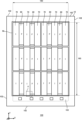
図1は、実施例に係る半導体装置100の上面図の一例を示す。図1においては、各部材を半導体基板10のおもて面に投影した位置を示している。図1においては、半導体装置100の一部の部材だけを示しており、一部の部材は省略している。
FIG. 1 shows an example of a top view of a
半導体装置100は、半導体基板10を備えている。半導体基板10は、上面視において端辺102を有する。本例の半導体基板10は、上面視において互いに向かい合う2組の端辺102を有する。X軸およびY軸は、何れかの端辺102と平行である。本明細書では、後述するトランジスタ部70およびダイオード部80の配列方向をX軸、上面視において配列方向と垂直な延伸方向をY軸と称す。またZ軸は、半導体基板10のおもて面と垂直である。
The
半導体基板10には活性領域160が設けられている。活性領域160は、半導体装置100が動作した場合に半導体基板10のおもて面と裏面との間で、深さ方向に主電流が流れる領域である。活性領域160の上方にはエミッタ電極52が設けられているが、図1では省略している。
An
図1では、活性領域160が後述するゲート配線層50よって分割されている。本例の活性領域160は、X軸方向に2つ、Y軸方向に3つに分割されてもよい。これらの活性領域160は、後述のエミッタ電極52により互いに電気的に接続されている。なお、ゲート配線層50によって分割される活性領域160の数は適宜変更してよい。
In FIG. 1, an
活性領域160には、トランジスタ部70とダイオード部80とが設けられている。例えば、半導体装置100は、トランジスタ部70に絶縁ゲート型バイポーラトランジスタ(IGBT:Insulated Gate Bipolar Tarnsistor)が設けられ、ダイオード部80に還流ダイオード(FWD:Free Wheeling Diode)が設けられた逆導通IGBT(RC-IGBT:Reverse Conducting IGBT)である。なお、半導体装置100は、IGBTであっても、MOSトランジスタであってもよい。
A
本例では、トランジスタ部70およびダイオード部80は、半導体基板10のおもて面において、配列方向(X軸方向)に沿って交互に配置されている。
In this example, the
図1においては、トランジスタ部70が配置される領域には記号「I」を付し、ダイオード部80が配置される領域には記号「F」を付している。トランジスタ部70およびダイオード部80は、それぞれ延伸方向に長手を有してよい。つまり、トランジスタ部70のY軸方向における長さは、X軸方向における幅よりも大きい。同様に、ダイオード部80のY軸方向における長さは、X軸方向における幅よりも大きい。トランジスタ部70およびダイオード部80の延伸方向と、後述する各トレンチ部の長手方向とは同一であってよい。
In FIG. 1, the region where the
図1では、トランジスタ部70のY軸方向の端部は、ダイオード部80のY軸方向の端部よりも活性領域160の外周側に位置している。また、トランジスタ部70のX軸方向の幅は、ダイオード部80のX軸方向の幅よりも広くなっている。
In FIG. 1, the end of the
ダイオード部80は、半導体基板10の裏面側に、N+型のカソード領域を有する。本明細書では、カソード領域が設けられた領域を、ダイオード部80と称する。つまりダイオード部80は、上面視においてカソード領域と重なる領域である。半導体基板10の裏面には、カソード領域以外の領域には、P+型のコレクタ領域が設けられてよい。
The
トランジスタ部70は、半導体基板10の裏面側に、P+型のコレクタ領域を有する。また、トランジスタ部70は、半導体基板10のおもて面側に、N型のエミッタ領域、P型のベース領域、ゲート導電部およびゲート絶縁膜を有するゲートトレンチ部が周期的に配置されている。
The
半導体装置100は、半導体基板10の上方に1つ以上のパッドを有してよい。一例として、半導体装置100は、パッド領域163を備えてもよい。パッド領域163は、ゲートパッド、温度検出用ダイオード(不図示)のアノードパッドとカソードパッドおよび電流センス(不図示)の電流検出パッド等のパッドを有してもよい。パッド領域163は、活性領域160と後述するエッジ終端構造部162との間に配置される。半導体装置100の実装時において、各パッドは、ワイヤ等の配線を介して外部の回路に接続されてよい。
The
ゲート配線層50は、後述するゲートトレンチ部内に設けられるゲート導電部44とゲートパッドとを電気的に接続する。本例のゲート配線層50は、上面視において活性領域160を囲んでいる。
The
本例の半導体装置100は、活性領域160と活性領域160に隣接するパッド領域163とが、エッジ終端構造部162に囲まれている。エッジ終端構造部162は、半導体基板10のおもて面側の電界集中を緩和する。エッジ終端構造部162は、複数のガードリングを有してよい。ガードリングは、半導体基板10のおもて面と接するP型の領域である。複数のガードリングを設けることで、活性領域160の上面側における空乏層を外側に伸ばすことができ、半導体装置100の耐圧を向上できる。エッジ終端構造部162は、活性領域160およびパッド領域163を囲んで環状に設けられたフィールドプレートおよびリサーフのうちの少なくとも一つをさらに備えていてもよい。
In the
図2は、図1における領域Aの一例を示す拡大図である。領域Aは、上面視において、半導体装置100のY軸方向負側における、トランジスタ部70およびダイオード部80とパッド領域163との境界周辺である。
FIG. 2 is an enlarged view showing an example of area A in FIG. Region A is around the boundary between the
トランジスタ部70は、半導体基板10の裏面側に設けられたコレクタ領域22を半導体基板10のおもて面に投影した領域である。本例のコレクタ領域22は、一例としてP+型である。トランジスタ部70は、IGBT等のトランジスタを含む。
The
ダイオード部80は、半導体基板10の裏面側に設けられたカソード領域82を半導体基板10のおもて面に投影した領域である。本例のカソード領域82は、一例としてN+型である。ダイオード部80は、半導体基板10のおもて面においてトランジスタ部70と隣接して設けられた還流ダイオード(FWD:Free Wheel Diode)等のダイオードを含む。
The
半導体基板10は、シリコン基板であってよく、炭化シリコン基板であってよく、窒化ガリウム等の窒化物半導体基板等であってもよい。本例の半導体基板10は、シリコン基板である。
The
本例の半導体装置100は、半導体基板10のおもて面において、ゲートトレンチ部40と、ダミートレンチ部30と、エミッタ領域12と、第1ベース領域14と、第2ベース領域84と、コンタクト領域15と、ウェル領域17とを備える。また、本例の半導体装置100は、半導体基板10のおもて面の上方に設けられたエミッタ電極52およびゲート配線層50を備える。
The
エミッタ電極52は、ゲートトレンチ部40、ダミートレンチ部30、エミッタ領域12、第1ベース領域14、第2ベース領域84、コンタクト領域15およびウェル領域17の上方に設けられている。また、ゲート配線層50は、ゲートトレンチ部40およびウェル領域17の上方に設けられている。
エミッタ電極52およびゲート配線層50は、金属を含む材料で形成される。エミッタ電極52の少なくとも一部の領域は、アルミニウム、またはアルミニウムを主成分とする合金(例えば、アルミニウム-シリコン合金、アルミニウム-シリコン-銅合金等)で形成されてよい。ゲート配線層50の少なくとも一部の領域は、アルミニウム、またはアルミニウムを主成分とする合金(例えば、アルミニウム‐シリコン合金、またはアルミニウム‐シリコン-銅合金等)で形成されてよい。エミッタ電極52およびゲート配線層50は、アルミニウム等で形成された領域の下層にチタンやチタン化合物等で形成されたバリアメタルを有してよい。エミッタ電極52およびゲート配線層50は、互いに電気的に分離して設けられている。
The
エミッタ電極52およびゲート配線層50は、層間絶縁膜38を挟んで、半導体基板10の上方に設けられている。層間絶縁膜38は、図2では省略されている。層間絶縁膜38には、コンタクトホール54、コンタクトホール55およびコンタクトホール56が貫通して設けられている。
The
コンタクトホール55は、トランジスタ部70のゲートトレンチ部40内のゲート導電部44とゲート配線層50とを接続する。コンタクトホール55の内部には、バリアメタルを介してタングステン等で形成されたプラグが設けられていてもよい。
The
コンタクトホール56は、トランジスタ部70およびダイオード部80に設けられた後述するダミートレンチ部30内のダミー導電部34とエミッタ電極52とを接続する。コンタクトホール56の内部には、バリアメタルを介してタングステン等で形成されたプラグが設けられていてもよい。
The
接続部25aでは、ゲート配線層50がコンタクトホール55を介して半導体基板10と電気的に接続する。接続部25bでは、エミッタ電極52がコンタクトホール56を介して半導体基板10と電気的に接続する。
At the
一例において、接続部25aは、ゲート配線層50とゲート導電部44との間の、コンタクトホール55内を含む領域に設けられている。接続部25bは、エミッタ電極52とダミー導電部34との間の、コンタクトホール56内を含む領域に設けられている。
In one example, the connecting
接続部25a、25bは、タングステンなどの金属や不純物がドープされたポリシリコン等の、導電性を有する材料である。また接続部25a、25bは、窒化チタンなどのバリアメタルを有していてもよい。ここでは、接続部25は、N型の不純物がドープされたポリシリコン(N+)である。接続部25a、25bは、酸化膜等の絶縁膜等を介して、半導体基板10のおもて面の上方に設けられている。
The connecting
ゲートトレンチ部40は、予め定められた配列方向(本例ではX軸方向)に沿って予め定められた間隔で配列される。本例のゲートトレンチ部40は、半導体基板10のおもて面に平行であって配列方向と垂直な延伸方向(本例ではY軸方向)に沿って延伸する2つの延伸部分39と、2つの延伸部分39を接続する接続部分41を有してよい。
The
接続部分41は、少なくとも一部が曲線状に形成されることが好ましい。ゲートトレンチ部40の2つの延伸部分39の端部を接続することで、延伸部分39の端部における電界集中を緩和できる。ゲートトレンチ部40の接続部分41において、ゲート配線層50がゲート導電部44と接続されてよい。
It is preferable that at least a portion of the connecting
ダミートレンチ部30は、その内部に設けられたダミー導電部34がエミッタ電極52と電気的に接続されたトレンチ部である。ダミートレンチ部30は、ゲートトレンチ部40と同様に、予め定められた配列方向(本例ではX軸方向)に沿って予め定められた間隔で配列される。本例のダミートレンチ部30は、ゲートトレンチ部40と同様に、半導体基板10のおもて面においてU字形状を有してよい。即ち、ダミートレンチ部30は、延伸方向に沿って延伸する2つの延伸部分29と、2つの延伸部分29を接続する接続部分31を有してよい。
The
本例のコンタクトホール54は、トランジスタ部70において、エミッタ領域12およびコンタクト領域15の各領域の上方に設けられている。コンタクトホール54は、ダイオード部80において、コンタクト領域15および第2ベース領域84の上方に設けられている。いずれのコンタクトホール54も、Y軸方向両端に設けられたウェル領域17の上方には設けられていない。このように、層間絶縁膜には、1または複数のコンタクトホール54が設けられている。1または複数のコンタクトホール54は、延伸方向に延伸して設けられてよい。
The
メサ部71およびメサ部81は、半導体基板10のおもて面と平行な面内において、トレンチ部に隣接して設けられたメサ部である。メサ部とは、隣り合う2つのトレンチ部に挟まれた半導体基板10の部分であって、半導体基板10のおもて面から、各トレンチ部の最も深い底部の深さまでの部分であってよい。各トレンチ部の延伸部分を1つのトレンチ部としてよい。即ち、2つの延伸部分に挟まれる領域をメサ部としてよい。
メサ部71は、トランジスタ部70において、ダミートレンチ部30またはゲートトレンチ部40の少なくとも1つに隣接して設けられている。
The
メサ部81は、ダイオード部80において、隣り合うダミートレンチ部30に挟まれた領域に設けられている。本例のメサ部81は、半導体基板10のおもて面において、第2ベース領域84を有し、Y軸方向の負側においてウェル領域17を有する。メサ部81には、第2ベース領域84のおもて面にコンタクト領域15が設けられていてもよい。
The
トランジスタ部70は、第1トランジスタ領域72と、第1トランジスタ領域72とダイオード部80との間に設けられた第2トランジスタ領域73と、第2トランジスタ領域73とダイオード部80との間に設けられた境界領域74とを有する。
The
第1トランジスタ領域72および第2トランジスタ領域73は、エミッタ領域12、コンタクト領域15および第1ベース領域14を有する。第1トランジスタ領域72および第2トランジスタ領域73のメサ部71は、半導体基板10のおもて面において、ウェル領域17と、エミッタ領域12と、第1ベース領域14と、コンタクト領域15とを有する。
The
第1トランジスタ領域72および第2トランジスタ領域73は、1つのゲートトレンチ部40と2つのダミートレンチ部30とを繰り返し配列させた構造を有する。即ち、本例の第1トランジスタ領域72および第2トランジスタ領域73は、1:2の比率でゲートトレンチ部40およびダミートレンチ部30を有している。例えば、トランジスタ部70は、2本の延伸部分39の間に2本の延伸部分29を有する。
The
但し、ゲートトレンチ部40およびダミートレンチ部30の比率は本例に限定されない。ゲートトレンチ部40とダミートレンチ部30の比率は、1:1であってもよく、2:3であってもよい。また、トランジスタ部70においてダミートレンチ部30を設けず、全てゲートトレンチ部40としてもよい。
However, the ratio of the
第1ベース領域14は、トランジスタ部70において、半導体基板10のおもて面側に設けられた領域である。第1ベース領域14は、一例としてP-型である。第1ベース領域14は、半導体基板10のおもて面において、第1トランジスタ領域72および第2トランジスタ領域73のメサ部71のY軸方向における両端部に設けられてよい。なお、図2は、当該第1ベース領域14のY軸方向の負側の端部のみを示している。
The
第2ベース領域84は、境界領域74およびダイオード部80において、半導体基板10のおもて面側に設けられた領域である。第2ベース領域84は、一例としてP--型である。第2ベース領域84のドーピング濃度は、第1ベース領域14のドーピング濃度よりも低い。第2ベース領域84は、半導体基板10のおもて面において、境界領域74のメサ部71およびメサ部81のY軸方向における両端部に設けられてよい。なお、図2は、当該第2ベース領域84のY軸方向の負側の端部のみを示している。ここで、ダイオード部80において、第2ベース領域84は、アノード層に相当する。
The
エミッタ領域12は、ドリフト領域18と同じ導電型で、ドリフト領域18よりもドーピング濃度の高い領域である。本例のエミッタ領域12は、一例としてN+型である。エミッタ領域12のドーパントの一例はヒ素(As)である。第1トランジスタ領域72および第2トランジスタ領域73において、エミッタ領域12は、ゲートトレンチ部40と接して設けられている。第1トランジスタ領域72および第2トランジスタ領域73において、エミッタ領域12は、メサ部71を挟んだ2本のトレンチ部の一方から他方まで、X軸方向に延伸して設けられてよい。エミッタ領域12は、コンタクトホール54の下方にも設けられている。
また、エミッタ領域12は、ダミートレンチ部30と接してもよいし、接しなくてもよい。本例のエミッタ領域12は、ダミートレンチ部30と接している。エミッタ領域12は、境界領域74およびメサ部81には設けられなくてよい。
Further, the
コンタクト領域15は、第1ベース領域14と同じ導電型で、第1ベース領域14よりもドーピング濃度の高い領域である。本例のコンタクト領域15は、一例としてP+型である。本例のコンタクト領域15は、メサ部71のおもて面に設けられている。第1トランジスタ領域72および第2トランジスタ領域73において、コンタクト領域15は、メサ部71を挟んだ2本のトレンチ部の一方から他方まで、X軸方向に延伸して設けられてよい。一方で、境界領域74において、コンタクト領域15のX軸方向端部は、隣接するトレンチ部から離間している。さらに境界領域74において、Y軸方向では、コンタクト領域15が選択的に設けられている。
The
コンタクト領域15は、ゲートトレンチ部40と接してもよいし、接しなくてもよい。また、コンタクト領域15は、ダミートレンチ部30と接してもよいし、接しなくてもよい。第1トランジスタ領域72および第2トランジスタ領域73において、コンタクト領域15は、ダミートレンチ部30およびゲートトレンチ部40と接する。一方で、境界領域74において、コンタクト領域15は、ダミートレンチ部30から離間している。コンタクト領域15は、コンタクトホール54の下方にも設けられている。
Contact
本例において、第1トランジスタ領域72および第2トランジスタ領域73のメサ部71には、エミッタ領域12およびコンタクト領域15が延伸方向(Y軸方向)において交互に設けられている。本例の第1トランジスタ領域72および第2トランジスタ領域73では、第1ベース領域14が半導体基板10のおもて面に露出していない。
In this example,
半導体基板10のおもて面において、第2トランジスタ領域73におけるコンタクト領域15の面積は、第1トランジスタ領域72におけるコンタクト領域15の面積よりも小さい。つまり、第2トランジスタ領域73では、コンタクト領域15のY軸方向長さに対するエミッタ領域12のY軸方向長さの比率が、第1トランジスタ領域72における同比率よりも大きい。
On the front surface of the
本例では、第1トランジスタ領域72の1つのコンタクト領域15の延伸方向(Y軸方向)長さをL1とし、当該コンタクト領域15と配列方向(X軸方向)において整列する第2トランジスタ領域73のコンタクト領域15の延伸方向(Y軸方向)長さをL2とすると、L2=L1であるか、またはL2=0である。つまり、第2トランジスタ領域73において、第1トランジスタ領域72のコンタクト領域15と配列方向において整列する位置には、L1と同じ延伸方向長さL2のコンタクト領域15またはエミッタ領域12が設けられている。配列方向(X軸方向)において、第2トランジスタ領域73の幅は、境界領域74の幅よりも狭くてよい。
In this example, the length in the extending direction (Y-axis direction) of one
トランジスタ部70をターンオフし、ダイオード部80が導通すると、カソード領域82からアノード層として動作する第2ベース領域84に電子電流が流れ、逆回復電流が発生する。電子電流が第2ベース領域84に到達すると電導度変調が起き、アノード層から正孔電流が流れる。
When the
このとき、トランジスタ部70の第1ベース領域14へも、カソード領域82から電子電流が拡散する。トランジスタ部70に向かって拡散した電子電流により、第1ベース領域14よりドーピング濃度の高いコンタクト領域15からの正孔注入が促進され、半導体基板10の正孔密度が増大するので、ダイオード部80のターンオフに伴って正孔が消滅するまでに時間がかかる。このため、逆回復ピーク電流が増大するとともに、逆回復損失が大きくなる。
At this time, electron current also diffuses from the
本例の第2トランジスタ領域73では、第1トランジスタ領域72よりもコンタクト領域15の面積比率を小さくすることにより、正孔注入を抑制し、逆回復損失を低減することができる。
In the
境界領域74は、トランジスタ部70内においてダイオード部80と隣接する、トランジスタとして動作しない領域である。境界領域74のメサ部71は、半導体基板10のおもて面において、ウェル領域17と、エミッタ領域12と、第2ベース領域84と、コンタクト領域15とを有する。
The
本例のダイオード部80において、コンタクト領域15は、ダミートレンチ部30と接しておらず、延伸方向(Y軸方向)および配列方向(X軸方向)において、第2ベース領域84に挟まれて設けられている。ダイオード部80は、平面視で、コンタクト領域15のX軸方向端部が隣接するダミートレンチ部30から離間しており、Y軸方向ではコンタクト領域15が選択的に設けられている。
In the
同様に、本例の境界領域74において、コンタクト領域15は、ダミートレンチ部30と接しておらず、延伸方向および配列方向において、第2ベース領域84に挟まれて設けられている。すなわち、境界領域74は、トランジスタ部70の一部であるが、ダイオード部80と同様のおもて面構造を有する。
Similarly, in the
このように、トランジスタ部70におけるダイオード部80側に、ドーピング濃度の低い第2ベース領域84を有する境界領域74を設けることにより、正孔注入を抑制し、逆回復損失を低減することができる。
In this way, by providing the
ウェル領域17は、後述するドリフト領域18よりも半導体基板10のおもて面側に設けられている。ウェル領域17は、半導体装置100のエッジ側に設けられたウェル領域の一例である。ウェル領域17は、一例としてP+型である。ウェル領域17は、ゲート配線層50が設けられた側の活性領域の端部から、予め定められた範囲で設けられている。ウェル領域17の拡散深さは、ゲートトレンチ部40およびダミートレンチ部30の深さよりも深くてよい。ゲートトレンチ部40およびダミートレンチ部30の、ゲート配線層50側の一部の領域は、ウェル領域17に設けられている。ゲートトレンチ部40およびダミートレンチ部30の延伸方向の端の底は、ウェル領域17に覆われてよい。
Well
図3は、図2におけるa-a'断面の一例を示す図である。a-a'断面は、トランジスタ部70において、コンタクト領域15を通過するXZ面である。本例の半導体装置100は、a-a'断面において、半導体基板10、層間絶縁膜38コンタクト領域15およびコレクタ電極24を有する。エミッタ電極52は、半導体基板10および層間絶縁膜38の上方に形成される。
FIG. 3 is a diagram showing an example of the aa' cross section in FIG. The aa' cross section is an XZ plane passing through the
ドリフト領域18は、半導体基板10に設けられた領域である。本例のドリフト領域18は、一例としてN-型である。ドリフト領域18は、半導体基板10において他のドーピング領域が形成されずに残存した領域であってよい。即ち、ドリフト領域18のドーピング濃度は半導体基板10のドーピング濃度であってよい。
バッファ領域20は、ドリフト領域18の下方に設けられた領域である。本例のバッファ領域20は、ドリフト領域18と同じ導電型であり、一例としてN型である。バッファ領域20のドーピング濃度は、ドリフト領域18のドーピング濃度よりも高い。バッファ領域20は、第1ベース領域14および第2ベース領域84の下面側から広がる空乏層がコレクタ領域22およびカソード領域82に到達することを防ぐフィールドストップ層として機能してよい。
コレクタ領域22は、トランジスタ部70においてバッファ領域20の下方に設けられた、ドリフト領域18と異なる導電型の領域である。カソード領域82は、ダイオード部80においてバッファ領域20の下方に設けられた、ドリフト領域18と同じ導電型の領域である。コレクタ領域22とカソード領域82との境界は、トランジスタ部70とダイオード部80との境界である。
コレクタ電極24は、半導体基板10の裏面23に形成される。コレクタ電極24は、金属等の導電材料または金属等の導電材料を積層して形成される。
第1ベース領域14は、第1トランジスタ領域72および第2トランジスタ領域73のメサ部71においてドリフト領域18の上方に設けられた、ドリフト領域18と異なる導電型の領域である。第2ベース領域84は、境界領域74のメサ部71およびメサ部81においてドリフト領域18の上方に設けられた、ドリフト領域18と異なる導電型の領域である。本例の第1ベース領域14は、一例としてP-型である。また、本例の第2ベース領域84は、一例としてP--型である。第2ベース領域84のドーピング濃度は、第1ベース領域14のドーピング濃度よりも低い。第1ベース領域14は、ゲートトレンチ部40に接して設けられている。第1ベース領域14は、ダミートレンチ部30に接して設けられてよい。一方で、本例の第2ベース領域84は、ダミートレンチ部30に接して設けられており、ゲートトレンチ部40には接していない。
The
エミッタ領域12は、第1ベース領域14と半導体基板10のおもて面21との間に設けられている。他の断面において、エミッタ領域12は、第1トランジスタ領域72および第2トランジスタ領域73において、メサ部71のおもて面に設けられてよい。本例のエミッタ領域12は、境界領域74のメサ部71およびメサ部81には設けられていない。エミッタ領域12は、ゲートトレンチ部40と接して設けられている。エミッタ領域12は、ダミートレンチ部30と接してもよいし、接しなくてもよい。
蓄積領域16は、ドリフト領域18よりも半導体基板10のおもて面21側に設けられた領域である。本例の蓄積領域16はドリフト領域18と同じ導電型であり、一例としてN型である。蓄積領域16は、トランジスタ部70に設けられている。本例の蓄積領域16は、第1トランジスタ領域72および第2トランジスタ領域73に設けられているが、境界領域74には設けられていない。蓄積領域16は、境界領域74およびダイオード部に設けられていてもよい。
The
また、蓄積領域16は、ゲートトレンチ部40に接して設けられている。蓄積領域16は、ダミートレンチ部30に接してもよいし、接しなくてもよい。蓄積領域16のドーピング濃度は、ドリフト領域18のドーピング濃度よりも高い。蓄積領域16を設けることで、キャリア注入促進効果(IE効果)を高めて、トランジスタ部70のオン電圧を低減できる。
Furthermore, the
本例では、第1ベース領域14の下面に1段目の蓄積領域16が設けられ、さらに1段目の蓄積領域16の下面に設けられたドリフト領域18を挟んで、2段目の蓄積領域16が設けられている。蓄積領域16の段数は、所望のキャリア注入促進効果に応じて適宜変更してよい。
In this example, a first-
1つ以上のゲートトレンチ部40および1つ以上のダミートレンチ部30は、半導体基板10のおもて面21に設けられている。各トレンチ部は、おもて面21からドリフト領域18まで設けられている。エミッタ領域12、第1ベース領域14、第2ベース領域84、コンタクト領域15および蓄積領域16の少なくともいずれかが設けられた領域においては、各トレンチ部はこれらの領域も貫通して、ドリフト領域18に到達する。トレンチ部がドーピング領域を貫通するとは、ドーピング領域を形成してからトレンチ部を形成する順序で製造したものに限定されない。トレンチ部を形成した後に、トレンチ部の間にドーピング領域を形成したものも、トレンチ部がドーピング領域を貫通しているものに含まれる。
One or more
ゲートトレンチ部40は、半導体基板10のおもて面21に設けられたゲートトレンチ、ゲート絶縁膜42およびゲート導電部44を有する。ゲート絶縁膜42は、ゲートトレンチの内壁を覆って設けられている。ゲート絶縁膜42は、ゲートトレンチの内壁の半導体を酸化または窒化して形成してよい。ゲート導電部44は、ゲートトレンチの内部においてゲート絶縁膜42よりも内側に設けられている。ゲート絶縁膜42は、ゲート導電部44と半導体基板10とを絶縁する。ゲート導電部44は、ポリシリコン等の導電材料で形成される。ゲートトレンチ部40は、半導体基板10のおもて面21において層間絶縁膜38により覆われている。
The
ゲート導電部44は、半導体基板10の深さ方向において、ゲート絶縁膜42を挟んでメサ部71側で隣接する第1ベース領域14と対向する領域を含む。ゲート導電部44に所定の電圧が印加されると、第1ベース領域14のうちゲートトレンチに接する界面の表層に、電子の反転層によるチャネルが形成される。
Gate
ダミートレンチ部30は、ゲートトレンチ部40と同一の構造を有してよい。ダミートレンチ部30は、半導体基板10のおもて面21側に形成されたダミートレンチ、ダミー絶縁膜32およびダミー導電部34を有する。ダミー絶縁膜32は、ダミートレンチの内壁を覆って設けられている。ダミー導電部34は、ダミートレンチの内部に設けられ、且つ、ダミー絶縁膜32よりも内側に設けられている。ダミー絶縁膜32は、ダミー導電部34と半導体基板10とを絶縁する。ダミートレンチ部30は、おもて面21において層間絶縁膜38により覆われる。
The
層間絶縁膜38は、半導体基板10のおもて面21に設けられている。層間絶縁膜38の上方には、エミッタ電極52が設けられている。層間絶縁膜38には、エミッタ電極52と半導体基板10とを電気的に接続するための1または複数のコンタクトホール54が設けられている。コンタクトホール55およびコンタクトホール56も同様に、層間絶縁膜38を貫通して設けられてよい。
The
なお、キャリア消滅を促進し、ターンオフ時の逆回復損失を低減する技術として、ドリフト領域18において、ライフタイムキラーを含むライフタイム制御領域を設けることが知られている。ライフタイムキラーは、例えば、ヘリウムイオン、水素イオン(プロトン)、重水素イオン等を注入することで、半導体基板の所定の深さ位置に形成される結晶欠陥である。ライフタイム制御領域は、ダイオード部のターンオフ時にベース領域で発生する正孔とカソード領域から注入される電子との再結合を促進し、逆回復時のピーク電流を抑制する。
Note that as a technique for promoting carrier extinction and reducing reverse recovery loss at turn-off, it is known to provide a lifetime control region including a lifetime killer in the
半導体基板10のおもて面21側において、ダイオード部80から境界領域74の少なくとも一部にわたって、ライフタイム制御領域が連続的に設けられてもよい。これにより、ダイオード部の導通時には、ダイオード部80の第2ベース領域84のみならず、トランジスタ部70の第1ベース領域14からカソード領域82に向かう正孔電流が発生するが、境界領域74に設けられたライフタイム制御領域85がキャリア消滅を促進し、ターンオフ時の逆回復損失を低減する。ライフタイム制御領域85は、Z軸方向にライフタイムキラーの濃度分布のピークを複数持つように設けられていてもよい。
On the
ここで、本例に係る半導体装置100の不純物注入工程の一例を説明する。半導体基板10に、蓄積領域16を形成するための不純物が、第1トランジスタ領域72および第2トランジスタ領域73を形成する領域にマスクを使用して注入され、次に、第2ベース領域84を形成するための不純物が、全面に注入される。次に、第1ベース領域14を形成するための不純物が、第1トランジスタ領域72および第2トランジスタ領域73を形成する領域に、マスクを使用して注入される。この後、半導体基板10のおもて面21に、エッチングにより複数のトレンチ部が形成される。
Here, an example of an impurity implantation process for the
次に、エミッタ領域12を形成するための不純物が、第1トランジスタ領域72および第2トランジスタ領域73を形成する領域に、マスクを使用して注入される。次に、コンタクト領域15を形成するための不純物が、第1トランジスタ領域72および第2トランジスタ領域73を形成する領域に、マスクを使用して注入され、境界領域74およびダイオード部80に、別のマスクを使用して注入される。この後、半導体基板10のおもて面21上に、層間絶縁膜38、エミッタ電極52等のおもて面金属層が形成される。
Next, impurities for forming the
図4は、半導体装置100の下面図の一例を示す。ここでは、半導体基板10の裏面23において活性領域160の一部のみを示し、エッジ終端構造部162は省略されている。また、半導体基板10の裏面23に設けられたコレクタ電極24も省略されている。
FIG. 4 shows an example of a bottom view of the
コレクタ領域22は、トランジスタ部70においてバッファ領域20の下方に設けられた、ドリフト領域18と異なる導電型の領域である。カソード領域82は、ダイオード部80においてバッファ領域20の下方に設けられた、ドリフト領域18と同じ導電型の領域である。コレクタ領域22とカソード領域82との境界は、トランジスタ部70とダイオード部80との境界である。延伸方向において、活性領域160の端部とカソード領域82の端部との間には、コレクタ領域22が設けられていてよい。
図5は、半導体装置100の下面図の他の例を示す。ここでは、図4と共通する説明は省略する。本例のカソード領域は、図4のカソード領域82に対応する第1導電型の第1カソード領域82と、第1カソード領域82よりも面積が小さい第2導電型の第2カソード領域83とを有する。
FIG. 5 shows another example of a bottom view of the
一例として、第2カソード領域83は、第1カソード領域82の一部に均等に設けられた領域である。本例の第2カソード領域83は、配列方向に延伸して設けられてよい。延伸方向において、第1カソード領域82は、第2カソード領域83よりも長い。第2カソード領域83は、コレクタ領域22と同じドーピング濃度であってよい。第2カソード領域83は、配列方向の端部において、コレクタ領域22と接していてよい。第2カソード領域83は、逆回復時のサージ電圧を抑制し、ダイオード部80の特性を改善する。
As an example, the
図6は、比較例に係る半導体装置1100の上面の拡大図の一例を示す。図7は、図6におけるa-a'断面の一例を示す図である。ここでは、図2と共通する部材の説明は省略し、相違点を中心に説明する。
FIG. 6 shows an example of an enlarged view of the top surface of a
比較例に係る半導体装置1100のトランジスタ部70は、第1トランジスタ領域72および境界領域74を有するが、半導体装置100のトランジスタ部70と異なり、第1トランジスタ領域72と境界領域74との間に第2トランジスタ領域73が設けられていない。
The
配列方向(X軸方向)において、半導体装置1100における境界領域74の幅は、半導体装置100における第2トランジスタ領域73および境界領域74の幅の総和よりも狭い。また、半導体装置1100における境界領域74の幅は、半導体装置100における境界領域74の幅よりも広い。
In the arrangement direction (X-axis direction), the width of the
すなわち、半導体装置1100では、第1トランジスタ領域72とダイオード部80との間の距離が、半導体装置100よりも短い。そのため、ダイオード部80の導通時には、第1トランジスタ領域72の第1ベース領域14からカソード領域82に向かう正孔電流が発生し、半導体基板10の正孔密度が増大するので、ダイオード部80のターンオフに伴って正孔が消滅するまでに時間がかかる。そのため、半導体装置1100では、半導体装置100よりも逆回復時のピーク電流が大きく、逆回復損失が大きくなる。
That is, in the
半導体装置100では、第1トランジスタ領域72と境界領域74との間に、第1トランジスタ領域72よりもコンタクト領域15の面積が小さい第2トランジスタ領域73が設けられていることにより、ダイオード部80の導通時にカソード領域82に向かう正孔電流が低減する。そのため、半導体装置100では、半導体装置1100よりも逆回復時のピーク電流が小さく、逆回復損失を低減することができる。
In the
また、半導体装置100における境界領域74の幅は半導体装置1100における境界領域74の幅よりも短く、これに代えて第2トランジスタ領域73を設けているので、トランジスタ動作に寄与しない無効領域を低減することができる。
Further, the width of the
図8は、実施例2に係る半導体装置200の上面図の一例を示す。ここでは、図2に示す半導体装置100と共通する構成の説明は省略し、相違点を中心に説明する。
FIG. 8 shows an example of a top view of the
本例の第1トランジスタ領域72および第2トランジスタ領域73では、第1ベース領域14が半導体基板10のおもて面21に露出している。本例の第1トランジスタ領域および第2トランジスタ領域73では、半導体基板10のおもて面21において、延伸方向(Y軸方向)において、コンタクト領域15が第1ベース領域14に挟まれている。つまり、本例では、半導体基板10のおもて面21において、エミッタ領域12とコンタクト領域15との間に、第1ベース領域14が露出している。
In the
第1トランジスタ領域72および第2トランジスタ領域73の形成プロセスの一例において、半導体基板10に第1ベース領域14が形成された後で、半導体基板10のおもて面21にエミッタ領域12が形成され、次いでコンタクト領域15が形成される。半導体基板10のおもて面21に露出する第1ベース領域14は、コンタクト領域15を形成するために注入された不純物がエミッタ領域12の端部まで拡散せずに残存した領域であってよい。なお、エミッタ領域12およびコンタクト領域15を形成する順序は逆であってもよい。
In an example of the process for forming the
このように、実施例2に係る半導体装置200も、第1トランジスタ領域72と境界領域74との間に第2トランジスタ領域73を設けることによって、逆回復損失を低減し、実施例1に係る半導体装置100と同様の効果を得ることができる。
In this way, the
図9は、実施例3に係る半導体装置300の上面図の一例を示す。ここでは、図8に示す半導体装置200と共通する構成の説明は省略し、相違点を中心に説明する。
FIG. 9 shows an example of a top view of a
本例の第2トランジスタ領域73において、コンタクト領域15の延伸方向(Y軸方向)長さL2は、配列方向(X軸方向)に整列する第1トランジスタ領域72におけるコンタクト領域15の延伸方向(Y軸方向)長さL1よりも短い。
In the
すなわち、本例では、第2トランジスタ領域73におけるコンタクト領域15の面積比率がさらに小さくなるので、さらに逆回復損失を低減することができる。
That is, in this example, since the area ratio of the
また、実施例2において説明したように、第1トランジスタ領域72および第2トランジスタ領域73の形成プロセスの一例において、半導体基板10に第1ベース領域14が形成された後で、半導体基板10のおもて面21にエミッタ領域12が形成され、次いでコンタクト領域15が形成される。本例では、コンタクト領域15の延伸方向(Y軸方向)長さL2が短いので、不純物注入時にマスク位置がずれた場合であっても、エミッタ領域12の範囲にまで拡散しづらく、予め設定された延伸方向(Y軸方向)長さでコンタクト領域15を形成することができる。
Further, as described in Example 2, in an example of the process of forming the
図10は、逆回復時におけるコレクタ電流Icの時間変化を示すグラフである。図10のグラフにおいて、実線は、第2トランジスタ領域73を有さない比較例に係る半導体装置(例えば、半導体装置1100)におけるコレクタ電流Ic、破線は、第2トランジスタ領域73を有する実施例に係る半導体装置(例えば、半導体装置100、半導体装置200および半導体装置300のいずれか)におけるコレクタ電流Icの挙動を示す。
FIG. 10 is a graph showing temporal changes in collector current Ic during reverse recovery. In the graph of FIG. 10, the solid line indicates the collector current Ic in the semiconductor device according to the comparative example (for example, the semiconductor device 1100) not having the
時間t1にトランジスタ部をターンオフし、ダイオード部80が導通すると、カソード領域82からアノード層として動作する第2ベース領域84に電子電流が流れ、逆回復電流が発生する。電子電流が第2ベース領域84に到達すると電導度変調が起き、アノード層から正孔電流が流れる。さらに、トランジスタ部70の第1ベース領域14へも、カソード領域82から電子電流が拡散する。
When the transistor section is turned off at time t1 and the
トランジスタ部70に向かって拡散した電子電流により、第1ベース領域14よりドーピング濃度の高いコンタクト領域15からの正孔注入が促進され、半導体基板10の正孔密度が増大するので、ダイオード部80のターンオフに伴って正孔が消滅するまでに時間がかかる。このため、逆回復ピーク電流Irpが増大するとともに、逆回復損失が大きくなる。
The electron current diffused toward the
ここで、比較例に係る半導体装置におけるコレクタ電流Icは、時間t2において逆回復ピーク電流Irpとなった後で漸減し、時間t3付近でほぼゼロとなる。逆回復ピーク電流Irpが大きいと電流がゼロになるまで時間がかかるため、発熱が増大し、逆回復損失が増大する。 Here, the collector current Ic in the semiconductor device according to the comparative example gradually decreases after reaching the reverse recovery peak current Irp at time t2, and becomes almost zero near time t3. If the reverse recovery peak current Irp is large, it takes time for the current to become zero, which increases heat generation and reverse recovery loss.
一方、実施例に係る半導体装置100は、トランジスタ部70の第1トランジスタ領域72と境界領域74との間に第2トランジスタ領域73を有する。
On the other hand, the
第1トランジスタ領域72とダイオード部80との間に第2トランジスタ領域73および境界領域74が介在することにより、第1トランジスタ領域72とダイオード部80との間の距離が長くなり、第1トランジスタ領域72からダイオード部80への正孔注入が抑制される。このように、実施例に係る半導体装置では、比較例に係る半導体装置よりも逆回復ピーク電流Irpが小さく、電流がゼロになるまでの時間も短くなるため、逆回復損失が低減される。
Since the
以上、本発明を実施の形態を用いて説明したが、本発明の技術的範囲は上記実施の形態に記載の範囲には限定されない。上記実施の形態に、多様な変更または改良を加えることが可能であることが当業者に明らかである。その様な変更または改良を加えた形態も本発明の技術的範囲に含まれ得ることが、特許請求の範囲の記載から明らかである。 Although the present invention has been described above using the embodiments, the technical scope of the present invention is not limited to the range described in the above embodiments. It will be apparent to those skilled in the art that various changes or improvements can be made to the embodiments described above. It is clear from the claims that such modifications or improvements may be included within the technical scope of the present invention.
特許請求の範囲、明細書、および図面中において示した装置、システム、プログラム、および方法における動作、手順、ステップ、および段階等の各処理の実行順序は、特段「より前に」、「先立って」等と明示しておらず、また、前の処理の出力を後の処理で用いるのでない限り、任意の順序で実現しうることに留意すべきである。特許請求の範囲、明細書、および図面中の動作フローに関して、便宜上「まず、」、「次に、」等を用いて説明したとしても、この順で実施することが必須であることを意味するものではない。 The order of execution of each process, such as the operation, procedure, step, and stage in the apparatus, system, program, and method shown in the claims, specification, and drawings, is specifically defined as "before" or "before". It should be noted that they can be implemented in any order unless the output of the previous process is used in the subsequent process. Even if the claims, specifications, and operational flows in the drawings are explained using "first," "next," etc. for convenience, this does not mean that it is essential to carry out the operations in this order. It's not a thing.
10・・・半導体基板、12・・・エミッタ領域、14・・・第1ベース領域、15・・・コンタクト領域、16・・・蓄積領域、17・・・ウェル領域、18・・・ドリフト領域、20・・・バッファ領域、21・・・おもて面、22・・・コレクタ領域、23・・・裏面、24・・・コレクタ電極、25a・・・接続部、25b・・・接続部、29・・・延伸部分、30・・・ダミートレンチ部、31・・・接続部分、32・・・ダミー絶縁膜、34・・・ダミー導電部、38・・・層間絶縁膜、39・・・延伸部分、40・・・ゲートトレンチ部、41・・・接続部分、42・・・ゲート絶縁膜、44・・・ゲート導電部、50・・・ゲート配線層、52・・・エミッタ電極、54・・・コンタクトホール、55・・・コンタクトホール、56・・・コンタクトホール、70・・・トランジスタ部、71・・・メサ部、72・・・第1トランジスタ領域、73・・・第2トランジスタ領域、74・・・境界領域、80・・・ダイオード部、81・・・メサ部、82・・・カソード領域、83・・・第2カソード領域、84・・・第2ベース領域、100・・・半導体装置、160・・・活性領域、162・・・エッジ終端構造部、163・・・パッド領域、200・・・半導体装置、300・・・半導体装置、1100・・・半導体装置
DESCRIPTION OF
Claims (14)
前記半導体基板は、
第1導電型のドリフト領域と、
前記ドリフト領域の上方に設けられた第2導電型の第1ベース領域と、
前記ドリフト領域の上方に設けられた、前記第1ベース領域よりもドーピング濃度が低い第2導電型の第2ベース領域と、
前記第1ベース領域の上方に設けられた、前記ドリフト領域よりもドーピング濃度が高い第1導電型のエミッタ領域と、
前記第1ベース領域および前記第2ベース領域の上方に設けられた、前記第1ベース領域よりもドーピング濃度が高い第2導電型のコンタクト領域と
を有し、
前記トランジスタ部は、
前記エミッタ領域、前記コンタクト領域および前記第1ベース領域が設けられた第1トランジスタ領域と、
前記エミッタ領域および前記コンタクト領域が設けられ、前記第1トランジスタ領域と前記ダイオード部との間に設けられた第2トランジスタ領域と、
前記第2ベース領域を含む、前記第2トランジスタ領域と前記ダイオード部との間に設けられた境界領域と
を有し、
前記半導体基板のおもて面において、前記第2トランジスタ領域における前記コンタクト領域の面積は、前記第1トランジスタ領域における前記コンタクト領域の面積よりも小さい
半導体装置。 A semiconductor device including a semiconductor substrate having a transistor part and a diode part and provided with a plurality of trench parts,
The semiconductor substrate is
a first conductivity type drift region;
a first base region of a second conductivity type provided above the drift region;
a second base region of a second conductivity type provided above the drift region and having a lower doping concentration than the first base region;
an emitter region of a first conductivity type provided above the first base region and having a higher doping concentration than the drift region;
a contact region of a second conductivity type provided above the first base region and the second base region and having a higher doping concentration than the first base region;
The transistor section includes:
a first transistor region provided with the emitter region, the contact region, and the first base region;
a second transistor region provided with the emitter region and the contact region and provided between the first transistor region and the diode section;
a boundary region provided between the second transistor region and the diode portion, including the second base region;
In the front surface of the semiconductor substrate, the area of the contact region in the second transistor region is smaller than the area of the contact region in the first transistor region. The semiconductor device.
請求項1に記載の半導体装置。 The semiconductor device according to claim 1, wherein in the first transistor region, the first base region is not exposed on the front surface of the semiconductor substrate.
請求項1に記載の半導体装置。 The semiconductor device according to claim 1, wherein in the first transistor region, the first base region is exposed on a front surface of the semiconductor substrate.
請求項3に記載の半導体装置。 4. The semiconductor device according to claim 3, wherein the contact region is sandwiched between the first base regions on the front surface of the semiconductor substrate in the first transistor region.
請求項1に記載の半導体装置。 The semiconductor device according to claim 1, wherein the length of the contact region in the second transistor region in the trench extension direction is shorter than the length of the contact region in the first transistor region aligned in the trench arrangement direction.
前記第2ベース領域は前記境界領域および前記ダイオード部に設けられている
請求項1に記載の半導体装置。 The first base region is provided in the first transistor region and the second transistor region,
The semiconductor device according to claim 1, wherein the second base region is provided in the boundary region and the diode section.
請求項1に記載の半導体装置。 The semiconductor device according to claim 1, wherein the width of the second transistor region is narrower than the width of the boundary region in the trench arrangement direction.
請求項1に記載の半導体装置。 The semiconductor device according to claim 1 , wherein the semiconductor substrate has a first conductivity type accumulation region having a higher doping concentration than the drift region.
請求項8に記載の半導体装置。 The semiconductor device according to claim 8, wherein the accumulation region is provided in the transistor section.
請求項8に記載の半導体装置。 The semiconductor device according to claim 8, wherein the accumulation region is provided in the second transistor region but not in the boundary region.
前記第2トランジスタ領域には、前記ゲートトレンチ部が少なくとも1つ設けられている
請求項1に記載の半導体装置。 The plurality of trench portions include a gate trench portion and a dummy trench portion,
The semiconductor device according to claim 1 , wherein at least one of the gate trench portions is provided in the second transistor region.
請求項1に記載の半導体装置。 The semiconductor device according to claim 1, wherein the boundary region and the diode section have a lifetime control region including a lifetime killer on the front surface side of the semiconductor substrate.
前記境界領域および前記ダイオード部において、前記コンタクト領域は、前記第2ベース領域に挟まれて設けられている
請求項1に記載の半導体装置。 The diode section has the contact region and the second base region,
The semiconductor device according to claim 1, wherein in the boundary region and the diode section, the contact region is provided between the second base regions.
前記ダイオード部は、
前記半導体基板の裏面に設けられた第1導電型の第1カソード領域と、
前記半導体基板の裏面に設けられ、前記第1カソード領域よりも面積が小さい第2導電型の第2カソード領域と
をさらに有する
請求項1に記載の半導体装置。 The transistor section further includes a collector region of a second conductivity type provided on the back surface of the semiconductor substrate,
The diode section is
a first cathode region of a first conductivity type provided on the back surface of the semiconductor substrate;
The semiconductor device according to claim 1, further comprising: a second cathode region of a second conductivity type, which is provided on the back surface of the semiconductor substrate and has a smaller area than the first cathode region.
Priority Applications (3)
| Application Number | Priority Date | Filing Date | Title |
|---|---|---|---|
| JP2022092892A JP2023179936A (en) | 2022-06-08 | 2022-06-08 | Semiconductor device |
| CN202310437374.9A CN117199110A (en) | 2022-06-08 | 2023-04-21 | Semiconductor device with a semiconductor device having a plurality of semiconductor chips |
| US18/306,250 US20230402533A1 (en) | 2022-06-08 | 2023-04-25 | Semiconductor device |
Applications Claiming Priority (1)
| Application Number | Priority Date | Filing Date | Title |
|---|---|---|---|
| JP2022092892A JP2023179936A (en) | 2022-06-08 | 2022-06-08 | Semiconductor device |
Publications (1)
| Publication Number | Publication Date |
|---|---|
| JP2023179936A true JP2023179936A (en) | 2023-12-20 |
Family
ID=88987543
Family Applications (1)
| Application Number | Title | Priority Date | Filing Date |
|---|---|---|---|
| JP2022092892A Pending JP2023179936A (en) | 2022-06-08 | 2022-06-08 | Semiconductor device |
Country Status (3)
| Country | Link |
|---|---|
| US (1) | US20230402533A1 (en) |
| JP (1) | JP2023179936A (en) |
| CN (1) | CN117199110A (en) |
-
2022
- 2022-06-08 JP JP2022092892A patent/JP2023179936A/en active Pending
-
2023
- 2023-04-21 CN CN202310437374.9A patent/CN117199110A/en active Pending
- 2023-04-25 US US18/306,250 patent/US20230402533A1/en active Pending
Also Published As
| Publication number | Publication date |
|---|---|
| CN117199110A (en) | 2023-12-08 |
| US20230402533A1 (en) | 2023-12-14 |
Similar Documents
| Publication | Publication Date | Title |
|---|---|---|
| US11735584B2 (en) | Semiconductor device | |
| JP5787853B2 (en) | Power semiconductor device | |
| US11532738B2 (en) | Semiconductor device | |
| JP7020570B2 (en) | Semiconductor devices and their manufacturing methods | |
| JP2024060027A (en) | Semiconductor Device | |
| JP7384287B2 (en) | semiconductor equipment | |
| US11094787B2 (en) | Method of manufacturing semiconductor device and semiconductor device | |
| CN113937159A (en) | Semiconductor device with a plurality of semiconductor chips | |
| CN111247639A (en) | Semiconductor device with a plurality of semiconductor chips | |
| JP7384274B2 (en) | Semiconductor device and semiconductor device manufacturing method | |
| CN114388612A (en) | Semiconductor device and method for manufacturing semiconductor device | |
| JP2023179936A (en) | Semiconductor device | |
| JP7364027B2 (en) | Semiconductor device and its manufacturing method | |
| WO2021145079A1 (en) | Semiconductor device | |
| JP7351419B2 (en) | Semiconductor device and semiconductor device manufacturing method | |
| WO2022264697A1 (en) | Semiconductor device | |
| WO2023084939A1 (en) | Semiconductor device manufacturing method and semiconductor device | |
| US20220149191A1 (en) | Semiconductor device | |
| US20240088221A1 (en) | Semiconductor device | |
| WO2022080495A1 (en) | Semiconductor device | |
| US20160049484A1 (en) | Semiconductor device | |
| JP2023135082A (en) | Semiconductor device | |
| JP2024013911A (en) | semiconductor equipment | |
| JP2023019322A (en) | Semiconductor device | |
| JP2023136874A (en) | Semiconductor device |