JP2022168564A - Image forming device and current control method - Google Patents
Image forming device and current control method Download PDFInfo
- Publication number
- JP2022168564A JP2022168564A JP2021074109A JP2021074109A JP2022168564A JP 2022168564 A JP2022168564 A JP 2022168564A JP 2021074109 A JP2021074109 A JP 2021074109A JP 2021074109 A JP2021074109 A JP 2021074109A JP 2022168564 A JP2022168564 A JP 2022168564A
- Authority
- JP
- Japan
- Prior art keywords
- image forming
- current
- forming apparatus
- signal
- image
- Prior art date
- Legal status (The legal status is an assumption and is not a legal conclusion. Google has not performed a legal analysis and makes no representation as to the accuracy of the status listed.)
- Granted
Links
Images
Landscapes
- Laser Beam Printer (AREA)
- Control Or Security For Electrophotography (AREA)
- Facsimile Image Signal Circuits (AREA)
Abstract
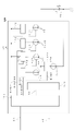
【課題】画像形成において画質を向上させる。【解決手段】画像形成装置が、入力画像データを入力する入力部と、前記入力画像データを構成する画素のうち、エッジとなる画素を検出する検出部と、前記エッジの濃度を変換して変換画素を生成する変換部と、前記変換画素に基づいて光を発する光源を用いて画像形成を行う画像形成部と、前記光源に流す電流を調整して、前記光の光量を調整する調整部とを備えることを特徴とする。【選択図】図11[Problem] To improve image quality in image formation. [Solution] An image forming device is characterized by comprising an input section for inputting input image data, a detection section for detecting pixels that become edges among the pixels constituting the input image data, a conversion section for converting the density of the edges to generate converted pixels, an image forming section for forming an image using a light source that emits light based on the converted pixels, and an adjustment section for adjusting the amount of light by adjusting the current flowing through the light source. [Selected Figure] Figure 11
Description
本発明は、画像形成装置、及び、電流制御方法に関する。 The present invention relates to an image forming apparatus and a current control method.
感光体ドラムに潜像を形成するため、光を感光体ドラムに当てる光源を備える画像形成装置が知られている。 2. Description of the Related Art An image forming apparatus is known which includes a light source for applying light to a photoreceptor drum in order to form a latent image on the photoreceptor drum.
そして、画像形成装置は、通常画素と強露光画素の境界領域を検出する。次に、画像形成装置は、境界領域の画素を光源が消灯する消灯画素に変換する。このようにすると、画像形成装置は、画像形成において、境界領域における通常画素の一部を強露光画素にし、かつ、残りの画素を消灯画素に変換する。すなわち、画像形成装置は、通常露光と強露光の間に消灯画素を設定する。これにより、オーバシュート電流、及び、アンダーシュート電流を精度良く補正できる技術が知られている(例えば、特許文献1を参照)。 Then, the image forming apparatus detects the boundary area between the normal pixels and the highly exposed pixels. Next, the image forming apparatus converts the pixels in the boundary area into extinguished pixels in which the light source is extinguished. In this way, the image forming apparatus converts some of the normal pixels in the boundary area into highly exposed pixels and converts the remaining pixels into unlit pixels during image formation. That is, the image forming apparatus sets off pixels between normal exposure and strong exposure. There is known a technique capable of correcting an overshoot current and an undershoot current with high accuracy (see, for example, Patent Document 1).
特許文献1に開示の技術は、エッジにおける濃度等を補正して、エッジ効果等を防ぐことができない場合がある。そのため、従来の技術は、エッジ等において、画質が悪い課題がある。 The technique disclosed in Japanese Patent Application Laid-Open No. 2002-200300 may not be able to prevent edge effects by correcting density and the like at edges. Therefore, the conventional technique has a problem of poor image quality at edges and the like.
本発明は、画像形成における画質の向上を目的とする。 An object of the present invention is to improve image quality in image formation.
上記の課題を解決するため、本発明の一態様である、画像形成装置は、
入力画像データを入力する入力部と、
前記入力画像データを構成する画素のうち、エッジとなる画素を検出する検出部と、
前記エッジの濃度を変換して変換画素を生成する変換部と、
前記変換画素に基づいて光を発する光源を用いて画像形成を行う画像形成部と、
前記光源に流す電流を調整して、前記光の光量を調整する調整部と
を備えることを特徴とする。
In order to solve the above problems, an image forming apparatus, which is one aspect of the present invention,
an input unit for inputting input image data;
a detection unit for detecting edge pixels among the pixels constituting the input image data;
a converting unit that converts the density of the edge to generate a converted pixel;
an image forming unit that forms an image using a light source that emits light based on the conversion pixels;
and an adjustment unit that adjusts the amount of light by adjusting the current flowing through the light source.
本発明によれば、画像形成において、画質を向上できる。 According to the present invention, image quality can be improved in image formation.
以下、添付する図面を参照し、具体例を説明する。なお、実施形態は、以下に説明する具体例に限られない。 A specific example will be described below with reference to the accompanying drawings. Note that the embodiments are not limited to the specific examples described below.
[画像形成装置例]
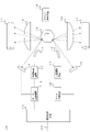
図1は、画像形成装置10の例を示す図である。例えば、画像形成装置10は、感光体11、レンズ12、ポリゴンミラー13、ポリゴン制御装置14、及び、レーザダイオード15(「LD」という場合もある。)等を備える。また、画像形成装置10は、検出装置16、光源駆動装置17、データ生成装置18、及び、画像処理装置19等を備える。以下、画像形成装置10は、図示するように、各ハードウェア資源を2つ備える例とする。
[Example of image forming apparatus]
FIG. 1 is a diagram showing an example of an
感光体11は、潜像を形成する。具体的には、感光体11は、レーザダイオード15が発する光が照射すると、光が照射された部分に潜像を形成する。そして、潜像の部分には、トナーが転写される。すなわち、感光体11には、記録媒体に画像形成する画像を示す潜像が形成される。
Photoreceptor 11 forms a latent image. Specifically, when the photoreceptor 11 is irradiated with light emitted from the
レンズ12、及び、ポリゴンミラー13は、光学部材の例である。なお、光学部材は、他にあってもよい。レンズ12は、例えば、Fθレンズである。そして、レンズ12を透過した光が感光体11に当たると、感光体11上に潜像が形成される。
The
ポリゴンミラー13は、レーザダイオード15が発する光を反射する。そして、ポリゴンミラー13が回転すると、光は、一方向(図では左右方向である。以下「主走査方向」という。)に走査する。
ポリゴン制御装置14は、ポリゴンミラー13を回転させるアクチュエータ等を制御する装置である。
The
レーザダイオード15は、光を発する光源装置の例である。例えば、レーザダイオード15は、半導体LD等である。
The
検出装置16は、主走査方向において、感光体11の延長上に設置する。そして、検出装置16は、受光すると検出信号を出力する。このようにして出力される検出信号は、基準とするタイミングを示す。例えば、検出信号は、画像データの書き出し位置を揃える等に用いる。
The
光源駆動装置17は、データ生成装置18が生成するデータ(以下「点灯データ」という。)に基づいて、レーザダイオード15を点灯、又は、消灯させる制御等を行う。
The light
データ生成装置18は、入力画像データ20等に基づいて、点灯データを生成する。
The
画像処理装置19は、Personal Computer(PC)、又は、スキャナ等の外部装置から、入力画像データ20等を入力する。なお、画像処理装置19は、入力画像データ20に対して、画像処理、及び、データの変換等を行ってもよい。
The
なお、画像形成装置10は、上記に示すようなハードウェア構成に限られない。したがって、画像形成装置10は、上記に示す以外のハードウェア資源を内部又は外部に備えてもよい。
Note that the
[処理例]
以下、説明を簡略にするため、エッジの検出、及び、補正の処理を中心に説明する。ただし、画像形成装置10は、以下に説明する以外の処理を更に行ってもよい。
[Processing example]
In order to simplify the explanation, the processing of edge detection and correction will be mainly explained below. However, the
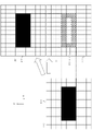
図2は、処理例を示す図(その1)である。以下、図2(A)に示す入力画像データ20を例に説明する。
FIG. 2 is a diagram (part 1) illustrating an example of processing. The
図2(A)は、画像形成を行う画素を黒色で示す。一方で、図2(A)は、画像形成を行わない画素を白色(すなわち、記録媒体の色のままとする点である。)で示す。 In FIG. 2A, pixels for image formation are shown in black. On the other hand, FIG. 2A shows pixels in which no image is formed in white (that is, the color of the recording medium remains unchanged).
例えば、画像形成装置10は、入力画像データ20に基づき、図2(B)に示す画像データ(以下「第1画像データ21」という。)、及び、図2(C)に示す画像データ(以下「第2画像データ22」という。)を生成する。なお、処理は、画像処理装置19が主に行う。
For example, based on the
第1画像データ21は、入力画像データ20と同一のデータである。
The
第2画像データ22は、エッジ30を検出した結果を示すデータである。
The
エッジ30は、例えば、注目画素、及び、周辺画素の濃度を比較して検出する。具体的には、画像形成装置10は、閾値を事前に設定する。次に、画像形成装置10は、注目画素と周辺画素の濃度が閾値以上に変化するか、すなわち、急激に濃度が変化する点か否かを判断する。そして、画像形成装置10は、注目画素が、急激に濃度が変化する画素であると判断すると、エッジ30と判断する。
The
図2(A)に示す例では、上下方向、又は、左右方向に、白色と黒色の画素が隣接すると、エッジ30が検出される。なお、エッジ30は、上下方向、及び、左右方向に限られず、斜め方向等に検出されてもよい。
In the example shown in FIG. 2A, an
なお、エッジ30の検出は、上記以外の処理で検出されてもよい。例えば、エッジ30は、フィルタ処理等で検出されてもよい。また、エッジ30は、隣接する画素だけでなく、注目画素の周辺に存在する画素を広く考慮して検出されてもよい。
The
以上のように、入力画像データ20に対し、エッジ30を検出する処理を行って、画像形成装置10は、第2画像データ22を生成する。次に、画像形成装置10は、第2画像データ22等に基づき、以下のようにエッジ30の濃度を変換する。
As described above, the
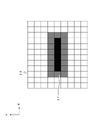
図3は、処理例を示す図(その2)である。図は、第1画像データ21、及び、第2画像データ22に基づいて、エッジ30の濃度を変換した後を示すデータ(以下「第3画像データ23」という。)の例を示す。
FIG. 3 is a diagram (part 2) showing an example of processing. The figure shows an example of data (hereinafter referred to as "
第3画像データ23は、第1画像データ21と比較すると、エッジ30の濃度が異なる。具体的には、第3画像データ23は、第1画像データ21が示す画像形成を行う画素(すなわち、第1画像データ21において、黒色の画素である。)のうち、エッジ30と検出された画素の濃度を変換して生成される。
When the
エッジ30、すなわち、変換対象となる画素は、第2画像データ22が示す画素である。以下、エッジ30の画素、すなわち、変換の対象とする画素を「変換画素31」という。一方で、画像形成装置10は、変換画素31以外の画素については、濃度等を第1画像データ21から維持する。
The
図示する例では、画像形成装置10は、エッジ30の濃度が低くなるように変換した例である。例えば、濃度は、事前に設定する値等に変換される。このように、エッジ30の濃度をどのような濃度に変換するかは、事前に設定される。
In the illustrated example, the
以上のように、第3画像データ23が生成されると、第3画像データ23に基づいて、画像形成装置10は、Pulse Width Modulation(PWM、パルス幅変調)変換等を行う。例えば、PWM変換は、データ生成装置18が主に行う。具体的には、図3に示す第3画像データ23は、以下のように変換する。
As described above, when the
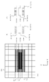
図4は、処理例を示す図(その3)である。以下、第3画像データ23を構成するラインのうち、第1ライン41、第2ライン42、及び、第3ライン43を対象とする例で説明する。
FIG. 4 is a diagram (part 3) showing an example of processing. In the following, an example in which the
図4(B)は、PWM変換結果の例を示す。具体的には、第11信号SIG11は、第1ライン41をPWM変換して生成する信号の例である。同様に、第12信号SIG12は、第2ライン42をPWM変換して生成する信号の例である。また、第13信号SIG13は、第3ライン43をPWM変換して生成する信号の例である。
FIG. 4B shows an example of PWM conversion results. Specifically, the eleventh signal SIG11 is an example of a signal generated by PWM-converting the
第11信号SIG11、第12信号SIG12、及び、第13信号SIG13は、濃度を光源が点灯する時間とする。すなわち、濃度を高くする画素は、Highレベルとなる幅が広い。一方で、濃度が低い画素は、Highレベルとなる幅が狭い。このように、PWM変換により、濃度を光源が点灯する時間の幅で示す信号が生成される。次に、図4(B)に示す信号は、位相制御により、例えば、図4(C)のように変換する。 The eleventh signal SIG11, the twelfth signal SIG12, and the thirteenth signal SIG13 use the time during which the light source is turned on as the density. In other words, pixels whose density is to be increased have a wide width of High level. On the other hand, pixels with low density have a narrow width of High level. In this way, the PWM conversion produces a signal that indicates the density by the width of the time that the light source is turned on. Next, the signal shown in FIG. 4(B) is converted by phase control, for example, as shown in FIG. 4(C).
図4(C)は、位相制御結果の例を示す。位相制御は、例えば、前後に大きなドットがある場合に、大きなドットがある方へ位相を寄せる制御である。 FIG. 4C shows an example of phase control results. The phase control is, for example, control to move the phase toward the large dot when there are large dots before and after.
第21信号SIG21、第22信号SIG22、及び、第23信号SIG23のうち、第21信号SIG21、及び、第23信号SIG23は、位相制御の前後で同じである。 Among the 21st signal SIG21, the 22nd signal SIG22, and the 23rd signal SIG23, the 21st signal SIG21 and the 23rd signal SIG23 are the same before and after the phase control.
一方で、第22信号SIG22は、位相を寄せるように変換されている点が異なる。このように、位相制御は、小さいドットと、大きいドットを1つのドットにまとめる処理である。このような位相制御がされた信号で画像形成が行われると、安定した画像が得られる。 On the other hand, the twenty-second signal SIG22 is different in that it is converted so as to shift the phase. Thus, phase control is a process of combining small dots and large dots into one dot. A stable image can be obtained by forming an image with such a phase-controlled signal.
これに対し、前後の画素で濃度が同程度の場合には、位相制御では、位相を寄せる処理を行わない。 On the other hand, when the densities of the preceding and following pixels are approximately the same, the phase control does not perform the process of shifting the phase.
以上のような処理により、画像形成装置10は、例えば、図4(C)に示すような点灯データを生成する。このように生成される点灯データに基づいて、光源が制御される。
Through the above processing, the
図5は、回路構成例を示す図である。 FIG. 5 is a diagram showing a circuit configuration example.
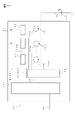
光源駆動装置17は、駆動信号生成回路171、スイッチ172、D/A変換器(以下「DAC173」という。)、及び、電流源174等を備える。
The light
駆動信号生成回路171は、点灯データ51を入力する。そして、点灯データ51に基づき、駆動信号生成回路171は、バイアス信号SIG31、オーバシュート信号SIG32、及び、点灯信号SIG33等の駆動信号を生成する。 The drive signal generation circuit 171 inputs the lighting data 51 . Then, based on the lighting data 51, the driving signal generation circuit 171 generates driving signals such as the bias signal SIG31, the overshoot signal SIG32, and the lighting signal SIG33.
点灯信号SIG33は、点灯データ51が示す信号である。 The lighting signal SIG33 is a signal indicated by the lighting data 51 .
スイッチ172は、バイアス信号SIG31、オーバシュート信号SIG32、及び、点灯信号SIG33等に基づいて、電源から供給する電流のON/OFFを切り替える。
The
DAC173は、電流データ53をアナログ量に変換する。そして、DAC173は、アナログ量を電流源174に入力する。
電流源174は、スイッチ172がONであると、アナログ量が示す電流をレーザダイオード15に流す。
The
以下、点灯信号SIG33に基づいて、電流源174が流す電流を「スイッチング電流Isw」という。オーバシュート信号SIG32に基づいて、電流源174が流す電流を「オーバシュート電流Iov」という。バイアス信号SIG31に基づいて、電流源174が流す電流を「バイアス電流Ib」という。
Hereinafter, the current supplied by the
そして、レーザダイオード15に流れる電流を「総電流It」という。なお、総電流Itは、駆動電流等という場合もある。
The current flowing through the
電流データ53、すなわち、電流源174が流す電流は、例えば、設定データ52等で設定する。なお、設定データ52は、例えば、動作モード等で定まってもよい。
The
[光量の調整例]
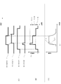
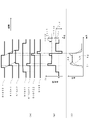
図6は、光量の調整例を示す図である。例えば、画像形成装置10は、レーザダイオード15が発する光の光量を図6(A)に示す信号に基づいて調整する。なお、調整は、光源駆動装置17が主に行う。
[Example of light intensity adjustment]
FIG. 6 is a diagram showing an example of adjusting the amount of light. For example, the
遅延信号SIG41は、点灯信号SIG33を遅らせた信号である。例えば、遅延信号SIG41は、遅延素子に点灯信号SIG33を入力する等で生成する。 The delayed signal SIG41 is a signal obtained by delaying the lighting signal SIG33. For example, the delay signal SIG41 is generated by inputting the lighting signal SIG33 to a delay element.
バイアス信号SIG31は、Highレベルになると、バイアス電流Ibが流れる信号である。以下、各信号は、Highレベルが「ON」であり、かつ、Lowレベルが「OFF」のHighActive信号であるとする。 The bias signal SIG31 is a signal that causes a bias current Ib to flow when it becomes High level. Hereinafter, each signal is assumed to be a HighActive signal whose High level is "ON" and whose Low level is "OFF".
バイアス電流Ibは、レーザダイオード15が発光を開始するのをスムーズにするために流す電流である。したがって、バイアス電流Ibは、レーザダイオード15が発光しない程度の電流である。例えば、バイアス電流Ibは、画像形成装置10が駆動している間、ON(図では、Highレベルである。)に設定する。また、バイアス電流Ibは、レーザダイオード15の特性等に応じて、事前に設定する。
The bias current Ib is a current that is caused to cause the
オーバシュート信号SIG32は、点灯信号SIG33の立ち上がり、すなわち、オーバシュートを検出した信号である。例えば、オーバシュート信号SIG32は、点灯信号SIG33がHighレベル、かつ、遅延信号SIG41がLowレベルであると、立ち上がりを検出してONとなる信号である。このように、点灯信号SIG33、及び、遅延信号SIG41を用いると、信号の立ち上がりを検出できる。 The overshoot signal SIG32 is a signal obtained by detecting the rise of the lighting signal SIG33, that is, the overshoot. For example, the overshoot signal SIG32 is a signal that detects a rise and turns ON when the lighting signal SIG33 is at High level and the delay signal SIG41 is at Low level. In this way, using the lighting signal SIG33 and the delay signal SIG41, it is possible to detect the rise of the signal.
なお、立ち下がりを検出する場合には、画像形成装置10は、点灯信号SIG33がLowレベル、かつ、遅延信号SIG41がHighレベルのタイミングを検出する。このように、点灯信号SIG33、及び、遅延信号SIG41を用いると、信号の立ち下がりを検出できる。
When detecting the fall, the
総電流Itは、図6(B)が示すように調整される。このように、電流を調整して光量が調整されるのが望ましい。具体的には、図6(B)のような調整の結果、光量は、図6(C)のようになる。 The total current It is adjusted as shown in FIG. 6(B). In this way, it is desirable to adjust the amount of light by adjusting the current. Specifically, as a result of the adjustment shown in FIG. 6(B), the light amount becomes as shown in FIG. 6(C).
図6(B)が示すように、バイアス信号SIG31がONになると、総電流Itは、バイアス電流Ibが流れる。さらに、点灯信号SIG33がONになると、総電流Itには、スイッチング電流Iswが加わる。同様に、オーバシュート信号SIG32がONになると、総電流Itは、オーバシュート電流Iovが流れる。このようにして定まる総電流Itに対し、光量は、図6(C)のような関係となる。 As shown in FIG. 6B, when the bias signal SIG31 is turned ON, the bias current Ib flows as the total current It. Further, when the lighting signal SIG33 is turned ON, the switching current Isw is added to the total current It. Similarly, when the overshoot signal SIG32 turns ON, the overshoot current Iov flows as the total current It. The amount of light has a relationship as shown in FIG. 6C with respect to the total current It determined in this manner.
第1タイミングT1では、点灯信号SIG33が立ち上がるため、オーバシュート信号SIG32がONとなる。したがって、第1タイミングT1から、オーバシュート信号SIG32がONの間、総電流Itは、下記(1)式に示すような電流となる。 At the first timing T1, the lighting signal SIG33 rises, so the overshoot signal SIG32 is turned ON. Therefore, from the first timing T1, while the overshoot signal SIG32 is ON, the total current It becomes a current as shown in the following equation (1).
It = Ib + Isw + Iov (1) It = Ib + Isw + Iov (1)
上記(1)式が示すように、総電流Itは、第1タイミングT1にオーバシュート電流Iovが流れるように調整される。このように、オーバシュート電流Iovは、バイアス電流Ib、及び、スイッチング電流Iswに追加して流す電流である。以下、オーバシュート電流Iov等で調整された後の光量を「調整後光量La」という。図は、調整後光量Laを実線で示す。 As shown by the above equation (1), the total current It is adjusted so that the overshoot current Iov flows at the first timing T1. Thus, the overshoot current Iov is a current added to the bias current Ib and the switching current Isw. Hereinafter, the amount of light after being adjusted by the overshoot current Iov or the like will be referred to as "adjusted amount of light La". In the drawing, the post-adjustment light amount La is indicated by a solid line.
オーバシュート電流Iovを流さないと、光量は、調整前光量Lb(図では、点線で示す光量である。)等のようになりやすい。調整前光量Lbのような現象は、光源、及び、光源を実装する基板等に存在する寄生容量等を要因とする。 If the overshoot current Iov is not applied, the light intensity tends to be the pre-adjustment light intensity Lb (the light intensity indicated by the dotted line in the drawing). A phenomenon such as the pre-adjustment light amount Lb is caused by the parasitic capacitance and the like existing in the light source and the substrate on which the light source is mounted.
寄生容量は、浮遊容量、又は、漂遊容量等とも呼ばれる。寄生容量は、例えば、電子部品等が有する静電容量である。 Parasitic capacitance is also called stray capacitance or the like. A parasitic capacitance is, for example, an electrostatic capacitance that an electronic component or the like has.
立ち上がり等では、寄生容量が充電されるまで寄生容量に電流が流れる。そのため、光源に流れる電流は、寄生容量に流れた分減少し、光量が調整前光量Lbのように鈍りやすい。そこで、寄生容量に電流が流れるのを想定し、総電流Itにオーバシュート電流Iovを加える。 During startup and the like, a current flows through the parasitic capacitance until the parasitic capacitance is charged. Therefore, the current flowing through the light source is reduced by the amount that flows through the parasitic capacitance, and the light intensity tends to be dull like the pre-adjustment light intensity Lb. Therefore, assuming that a current flows through the parasitic capacitance, the overshoot current Iov is added to the total current It.
オーバシュート電流Iovを流すように調整すると、寄生容量に流れる電流が補填されて第1タイミングT1において、光量は、調整後光量Laのように急峻に立ち上げることができる。 When the overshoot current Iov is adjusted to flow, the current flowing through the parasitic capacitance is compensated for, and the light amount can rise sharply like the post-adjustment light amount La at the first timing T1.
光量を多くすると、潜像に付着するトナー量が増える。そこで、エッジ30等に対して、エッジ効果を軽減させるため、画像形成装置10は、エッジ30の濃度を下げるように変換する。しかし、濃度を下げる変換を行うと、エッジ30が薄くなりやすい。そこで、オーバシュート電流Iovを流す等の調整により、画像形成装置10は、光量をエッジ効果が起きにくく、かつ、トナー量が最適となるように調整する。このようにして、濃度、及び、トナー量を最適化する。そして、トナー量の最適化により、画像形成装置10は、画質を向上できる。
Increasing the amount of light increases the amount of toner adhering to the latent image. Therefore, in order to reduce the edge effect on the
なお、画像形成を行う速度(「印刷速度」、又は、「線速」等でもよい。)によって、1ドットを形成する時間が異なる場合がある。このような場合には、オーバシュート電流Iovが1ドットの形成に占める割合も異なる。したがって、オーバシュート電流Iovは、画像形成を行う速度等に応じて決定されるのが望ましい。このように、画像形成装置10は、画像形成を行う速度等に応じてオーバシュート電流Iovを決定すると、画像形成を行う速度に適した画像処理、及び、電流制御ができる。
Note that the time required to form one dot may vary depending on the image forming speed ("printing speed" or "linear speed" may be used). In such a case, the ratio of the overshoot current Iov to the formation of one dot is also different. Therefore, the overshoot current Iov is desirably determined according to the image forming speed and the like. Thus, the
[第1変形例]
画像形成装置10は、以下のような構成でもよい。
[First modification]
The
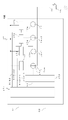
図7は、第1変形例における回路構成例を示す図である。図5と比較すると、図7に示す回路構成は、オーバシュート用の電流源174が2つになる点が異なる。以下、異なる点を中心に説明し、重複する説明を省略する。
FIG. 7 is a diagram showing a circuit configuration example in the first modified example. Compared to FIG. 5, the circuit configuration shown in FIG. 7 differs in that there are two
以下、第1オーバシュート信号SIG321に基づいて、電流源174が流す電流を「第1オーバシュート電流Iov1」という。第2オーバシュート信号SIG322に基づいて、電流源174が流す電流を「第2オーバシュート電流Iov2」という。
Hereinafter, the current supplied by the
また、第1変形例では、スイッチング電流Iswは、遅延信号SIG41がONとなると流れる。 Further, in the first modification, the switching current Isw flows when the delay signal SIG41 is turned ON.
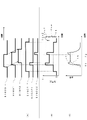
図8は、第1変形例における光量の調整例を示す図である。図6と比較すると、第2遅延信号SIG42が加わる点が異なる。また、オーバシュート信号SIG32が、第1オーバシュート信号SIG321、及び、第2オーバシュート信号SIG322となる点が異なる。以下、同様の信号については同一の符号を付し、説明を省略する。 FIG. 8 is a diagram showing an example of adjusting the amount of light in the first modified example. Compared to FIG. 6, it differs in that the second delay signal SIG42 is added. Another difference is that the overshoot signal SIG32 becomes a first overshoot signal SIG321 and a second overshoot signal SIG322. Hereinafter, similar signals are denoted by the same reference numerals, and descriptions thereof are omitted.
第1オーバシュート信号SIG321は、図6におけるオーバシュート信号SIG32と同様の信号である。すなわち、第1オーバシュート信号SIG321は、遅延信号SIG41の立ち上がりを示す信号である。 The first overshoot signal SIG321 is a signal similar to the overshoot signal SIG32 in FIG. That is, the first overshoot signal SIG321 is a signal that indicates the rise of the delay signal SIG41.
例えば、第1オーバシュート信号SIG321は、遅延信号SIG41がHighレベル、かつ、第2遅延信号SIG42がLowレベルであると、ONとなる信号である。このように、遅延信号SIG41、及び、第2遅延信号SIG42を用いると、立ち上がりを検出できる。 For example, the first overshoot signal SIG321 is a signal that turns ON when the delay signal SIG41 is at High level and the second delay signal SIG42 is at Low level. In this way, using the delay signal SIG41 and the second delay signal SIG42, the rise can be detected.
第1オーバシュート信号SIG321は、図6と同様に、第1タイミングT1に第1オーバシュート電流Iov1を流すように制御する。 The first overshoot signal SIG321 controls the first overshoot current Iov1 to flow at the first timing T1, as in FIG.
第2遅延信号SIG42は、遅延素子等により、点灯信号SIG33を遅延信号SIG41より更に遅らせた信号である。 The second delay signal SIG42 is a signal obtained by further delaying the lighting signal SIG33 from the delay signal SIG41 by a delay element or the like.
第2オーバシュート信号SIG322は、遅延信号SIG41の立ち下がりを示す信号である。 The second overshoot signal SIG322 is a signal that indicates the fall of the delay signal SIG41.
例えば、第2オーバシュート信号SIG322は、点灯信号SIG33がLowレベル、かつ、遅延信号SIG41がHighレベルであると、ONとなる信号である。このように、点灯信号SIG33、及び、遅延信号SIG41を用いると、立ち下がりを検出できる。 For example, the second overshoot signal SIG322 is a signal that turns ON when the lighting signal SIG33 is at Low level and the delay signal SIG41 is at High level. In this way, using the lighting signal SIG33 and the delay signal SIG41 makes it possible to detect the fall.
第2オーバシュート信号SIG322がONとなる第2タイミングT2では、第2オーバシュート電流Iov2が流れる。 At the second timing T2 when the second overshoot signal SIG322 turns ON, the second overshoot current Iov2 flows.
したがって、第1変形例では、第1タイミングT1では、総電流Itは、下記(2)式の通りとなる。 Therefore, in the first modification, at the first timing T1, the total current It is expressed by the following equation (2).
It = Ib + Isw + Iov1 (2) It = Ib + Isw + Iov1 (2)
また、第2タイミングT2では、総電流Itは、下記(3)式の通りとなる。 Further, at the second timing T2, the total current It is expressed by the following formula (3).
It = Ib + Isw + Iov2 (3) It = Ib + Isw + Iov2 (3)
以上のように、画像形成装置10は、電流の立ち上がりを第1オーバシュート電流Iov1で調整し、かつ、光源が消灯する直前も、第2オーバシュート電流Iov2で調整する。このように調整すると、画像形成装置10は、調整後光量Laのように、電流の立ち上がり、及び、電流の立下りの両タイミングにおいて、光量を増やすように調整できる。
As described above, the
例えば、図2に示すようなエッジ30の場合には、画像形成装置10は、左端に位置するエッジ30と、右端に位置するエッジ30の両方でトナー量を最適化できる。
For example, in the case of the
[第2変形例]
図9は、第2変形例における回路構成例を示す図である。第1変形例と比較すると、第2変形例は、アンダーシュート用の電流源174等が加わる点が異なる。以下、第1変形例と異なる点を中心に説明する。
[Second modification]
FIG. 9 is a diagram showing a circuit configuration example in the second modification. Compared to the first modification, the second modification differs in that a
以下、アンダーシュート信号SIG5に基づいて、電流源174が流す電流を「アンダーシュート電流Iud」という。すなわち、アンダーシュート信号SIG5をONにすると、アンダーシュート電流Iudが流れる。
Hereinafter, the current supplied by the
アンダーシュート電流Iudは、第1オーバシュート電流Iov1等の光源を発光させる電流とは逆方向に流す電流である。 The undershoot current Iud is a current that flows in the opposite direction to the current that causes the light source to emit light, such as the first overshoot current Iov1.
図10は、第2変形例における光量の調整例を示す図である。 FIG. 10 is a diagram showing an example of light amount adjustment in the second modified example.
アンダーシュート信号SIG5は、遅延信号SIG41の立ち下がりを示す信号である。 The undershoot signal SIG5 is a signal that indicates the fall of the delay signal SIG41.
例えば、アンダーシュート信号SIG5は、遅延信号SIG41がLowレベル、かつ、第2遅延信号SIG42がHighレベルであると、ONとなる信号である。このように、遅延信号SIG41、かつ、第2遅延信号SIG42を用いると、立ち下がりを検出できる。 For example, the undershoot signal SIG5 is a signal that turns ON when the delay signal SIG41 is at Low level and the second delay signal SIG42 is at High level. In this way, using the delayed signal SIG41 and the second delayed signal SIG42, the trailing edge can be detected.
アンダーシュート電流Iudが無いと、寄生容量に保持されている電荷等が光源に流れて、光量が調整前光量Lbのように鈍りやすい。 Without the undershoot current Iud, the electric charge held in the parasitic capacitance flows into the light source, and the light intensity tends to be dull like the pre-adjustment light intensity Lb.
一方で、アンダーシュート電流Iudを流すように調整すると、光量は、調整後光量Laのように急峻に立ち下げることができる。 On the other hand, if the undershoot current Iud is adjusted to flow, the light intensity can drop sharply like the post-adjustment light intensity La.
以上のように、画像形成装置10は、電流の立ち上がりを第1オーバシュート電流Iov1で調整し、かつ、光源が消灯する直前も、第2オーバシュート電流Iov2で調整する。
As described above, the
調整前光量Lbのように光源を消灯させるのが遅いと、画像形成を行う位置と、画像形成を行わない位置との境界等で、不要なドットを形成してしまう場合がある。 If the light source is turned off slowly as in the pre-adjustment light amount Lb, unnecessary dots may be formed at the boundary between the position where image formation is performed and the position where image formation is not performed.
そこで、画像形成装置10は、調整後光量Laのように、境界で電流を急峻に立ち下げるように調整する。このようにすると、不要なトナーが付着するのを防ぎ、画質を向上できる。また、不要なトナーが付着するのを防ぎ、トナー量を最適化できる。
Therefore, the
[動作モード等に基づく処理例]
画像形成装置10は、例えば、以下のように動作モード等を考慮して処理を行うのが望ましい。
[Example of processing based on operation mode, etc.]
It is desirable that the
動作モードは、例えば、コピー、又は、プリンタ等の画像形成装置10が行う画像形成の用途等を示す情報である。例えば、動作モードは、ユーザの操作によって設定される。
The operation mode is, for example, information indicating the purpose of image formation performed by the
動作モードが異なると、要求される画質が異なる場合が多い。そのため、画像形成装置10は、動作モードによっては、異なる画像処理を行う。例えば、動作モードが異なると、エッジ30に対する補正の処理が異なる。
Different modes of operation often require different image quality. Therefore, the
ゆえに、動作モードに基づいて電流を調整すると、画像形成装置10は、より最適な画像処理と電流制御ができる。
Therefore, adjusting the current based on the operating mode allows the
また、動作モードと同様に、画像形成を行う速度、画質、又は、記録媒体の種類等の条件が異なると、要求される画質が異なる場合がある。したがって、画像形成装置10は、画像形成を行う速度、画質、又は、記録媒体の種類等の条件に基づいて電流を調整すると、画像形成装置10は、より最適な画像処理と電流制御ができる。
Also, as with the operation modes, the required image quality may differ depending on conditions such as image forming speed, image quality, or type of recording medium. Therefore, if the
[機能構成例]
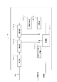
図11は、機能構成例を示す図である。例えば、画像形成装置10は、入力部10F1、検出部10F2、変換部10F3、画像形成部10F4、調整部10F5、及び、作像部10F7等を備える。なお、画像形成装置10は、図示するように、動作モード設定部10F6を更に備えるのが望ましい。以下、図示する機能構成を例に説明する。
[Example of functional configuration]
FIG. 11 is a diagram illustrating a functional configuration example. For example, the
入力部10F1は、入力画像データ20を入力する入力手順を行う。例えば、入力部10F1は、画像処理装置19が有する入力装置等で実現する。
The input unit 10F1 performs an input procedure for inputting the
検出部10F2は、入力画像データ20を構成する画素のうち、エッジとなる画素を検出する検出手順を行う。例えば、入力部10F1は、画像処理装置19が有する演算装置等で実現する。
The detection unit 10F2 performs a detection procedure for detecting edge pixels among the pixels forming the
変換部10F3は、エッジの濃度を変換して変換画素を生成する変換手順を行う。例えば、変換部10F3は、画像処理装置19が有する演算装置等で実現する。
The conversion unit 10F3 performs a conversion procedure for converting the density of the edge to generate a converted pixel. For example, the conversion unit 10F3 is implemented by an arithmetic device or the like included in the
画像形成部10F4は、変換画素に基づいて光を発する光源を用いて画像形成を行う画像形成手順を行う。例えば、画像形成部10F4は、光源駆動装置17等で実現する。
The image forming section 10F4 performs an image forming procedure of forming an image using a light source that emits light based on the converted pixels. For example, the image forming section 10F4 is realized by the light
調整部10F5は、光源に流す電流を調整して、光量を調整する調整手順を行う。例えば、調整部10F5は、光源駆動装置17等で実現する。
The adjustment unit 10F5 performs an adjustment procedure for adjusting the amount of light by adjusting the current flowing through the light source. For example, the adjustment unit 10F5 is realized by the light
動作モード設定部10F6は、動作モードを設定する動作モード設定手順を行う。例えば、動作モード設定部10F6は、画像処理装置19が有する入力装置等で実現する。入力装置は、ユーザ操作等によって動作モード等を受け付ける。
The operation mode setting unit 10F6 performs an operation mode setting procedure for setting the operation mode. For example, the operation mode setting unit 10F6 is implemented by an input device or the like that the
作像部10F7は、例えば、レーザダイオード15、及び、感光体11等である。
The imaging unit 10F7 is, for example, a
画像形成装置10は、記録媒体に画像形成を行い、印刷物等を出力する。
The
以上のような構成であると、画像形成装置10は、エッジの濃度を変換してエッジ効果等を防ぐレベルまで濃度を下げる補正が可能である。すなわち、従来の技術では、エッジ効果を防げる程度まで濃度を下げられない場合がある。一方で、本願のような構成では、画像形成装置10は、エッジ効果等を防ぐレベルまで十分に濃度を下げる補正ができる。ゆえに、画像形成装置10は、エッジ効果等を防いで画質を向上できる。
With the configuration as described above, the
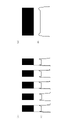
図12は、エッジ効果の例を示す図である。例えば、図12(A)、又は、図12(B)のような画像形成を行う場合には、図12(C)、及び、図12(D)のような信号を用いて画像形成を行う場合がある。 FIG. 12 is a diagram showing an example of the edge effect. For example, when performing image formation as shown in FIG. 12(A) or FIG. 12(B), image formation is performed using signals such as those shown in FIGS. 12(C) and 12(D). Sometimes.
このような信号を用いると、エッジとなる位置で無駄にトナーが付着する現象、いわゆるエッジ効果が起きる。このようなエッジ効果が発生するのを防ぐため、画像形成装置10は、エッジの濃度を下げるように補正する。例えば、画像形成装置10は、図3に示すように処理を行う。そして、画像形成装置10は、変換画素に基づいて画像形成を行う。
When such a signal is used, a so-called edge effect occurs, which is a phenomenon in which toner is unnecessarily adhered at edge positions. In order to prevent such an edge effect from occurring, the
画像形成を行う際に、画像形成装置10は、光源に流す電流の立ち上がり、及び、立ち下がり等において、電流を調整して光源が発する光量を調整する。このように、電流で光量を調整すると、微調整が可能である。
When forming an image, the
また、従来の技術では、エッジ効果を抑制できるほど濃度を下げると画質が悪化する場合がある。一方で、上記に示す画像形成装置10は、濃度を下げても、電流を調整して光量を調整するため、トナー量を最適化して画質を向上できる。
Further, in the conventional technique, if the density is lowered to the extent that the edge effect can be suppressed, the image quality may deteriorate. On the other hand, the
[その他の実施形態]
上記に説明した電流制御方法は、例えば、一部の処理をファームウェア等のプログラム等で実現してもよい。すなわち、電流制御方法は、プログラムに基づいて、演算装置、記憶装置、入力装置、出力装置、及び、制御装置を協働して動作させて、コンピュータが実行する方法である。また、プログラムは、記憶装置、又は、記憶媒体等に書き込まれて配布、又は、電気通信回線等を通じて配布されてもよい。
[Other embodiments]
In the current control method described above, for example, part of the processing may be realized by a program such as firmware. That is, the current control method is a method that is executed by a computer by cooperatively operating an arithmetic device, a memory device, an input device, an output device, and a control device based on a program. Also, the program may be written in a storage device or storage medium and distributed, or may be distributed through an electric communication line or the like.
上記に説明した各装置は、1つの装置でなくともよい。すなわち、各装置は、複数の装置で構成するシステム等でもよい。 Each device described above need not be one device. That is, each device may be a system or the like composed of a plurality of devices.
画像形成装置は、例えば、商用印刷機(例えば、大型の電子写真プリンタ、又は、インクジェットプリンタ等である。)等でもよい。 The image forming apparatus may be, for example, a commercial printing machine (for example, a large electrophotographic printer, an inkjet printer, or the like).
記録媒体は、例えば、用紙(「普通紙」等ともいう。)である。ただし、記録媒体は、用紙以外のコート紙、ラベル紙等の他、オーバヘッドプロジェクタシート、フィルム、又は、可撓性を持つ薄板等でもよい。また、記録媒体は、ロール紙等でもよい。 The recording medium is, for example, paper (also called “plain paper” or the like). However, the recording medium may be coated paper, label paper, etc., overhead projector sheet, film, flexible thin plate, or the like. Also, the recording medium may be roll paper or the like.
すなわち、記録媒体の素材は、インク滴、又は、トナー等の塗料が付着可能、一時的に付着可能、付着して固着、又は、付着して浸透する材質等であればよい。 In other words, the material of the recording medium may be any material to which ink droplets or paint such as toner can adhere, which can adhere temporarily, which adheres and adheres, or which adheres and permeates.
具体的には、記録媒体は、用紙、フィルム、若しくは、布等の被記録媒体、電子基板、圧電素子(「圧電部材」等ともいう。)等の電子部品、粉体層(「粉末層」等ともいう。)、臓器モデル、又は、検査用セル等である。 Specifically, the recording medium includes recording media such as paper, film, or cloth, electronic substrates, electronic components such as piezoelectric elements (also referred to as “piezoelectric members”), powder layers (“powder layers”), and the like. etc.), an organ model, an inspection cell, or the like.
このように、記録媒体の材質は、塗料が付着可能であって、紙、糸、繊維、布帛、皮革、金属、プラスチック、ガラス、木材、セラミックス、又は、これらの組み合わせ等であればよい。 As described above, the material of the recording medium may be paper, thread, fiber, fabric, leather, metal, plastic, glass, wood, ceramics, or a combination thereof, to which paint can be applied.
なお、本発明は、上記に例示する各実施形態に限定されるものではなく、その技術的要旨を逸脱しない範囲で種々の変形が可能であり、特許請求の範囲に記載された技術思想に含まれる技術的事項のすべてが本発明の対象となる。上記実施形態は、好適な例を示したものであるが、当業者であれば、開示した内容から様々な変形例を実現することが可能である。そのような変形例も、特許請求の範囲に記載された技術的範囲に含まれる。 It should be noted that the present invention is not limited to the embodiments illustrated above, and various modifications are possible without departing from the technical scope of the invention. All technical matters covered by the present invention are covered by the present invention. Although the above embodiments show preferred examples, those skilled in the art can realize various modifications from the disclosed contents. Such modifications are also included in the technical scope described in the claims.
10 :画像形成装置
10F1 :入力部
10F2 :検出部
10F3 :変換部
10F4 :画像形成部
10F5 :調整部
10F6 :動作モード設定部
20 :入力画像データ
30 :エッジ
31 :変換画素
Ib :バイアス電流
Iov :オーバシュート電流
Iov1 :第1オーバシュート電流
Iov2 :第2オーバシュート電流
Isw :スイッチング電流
It :総電流
Iud :アンダーシュート電流
La :調整後光量
Lb :調整前光量
SIG32 :オーバシュート信号
SIG321 :第1オーバシュート信号
SIG322 :第2オーバシュート信号
SIG5 :アンダーシュート信号
T1 :第1タイミング
T2 :第2タイミング
10: Image forming apparatus 10F1: Input unit 10F2: Detecting unit 10F3: Converting unit 10F4: Image forming unit 10F5: Adjusting unit 10F6: Operation mode setting unit 20: Input image data 30: Edge 31: Converted pixel Ib: Bias current Iov: Overshoot current Iov1: First overshoot current Iov2: Second overshoot current Isw: Switching current It: Total current Iud: Undershoot current La: Light intensity after adjustment Lb: Light intensity before adjustment SIG32: Overshoot signal SIG321: First overshoot Shoot signal SIG322: Second overshoot signal SIG5: Undershoot signal T1: First timing T2: Second timing
Claims (6)
前記入力画像データを構成する画素のうち、エッジとなる画素を検出する検出部と、
前記エッジの濃度を変換して変換画素を生成する変換部と、
前記変換画素に基づいて光を発する光源を用いて画像形成を行う画像形成部と、
前記光源に流す電流を調整して、前記光の光量を調整する調整部と
を備える画像形成装置。 an input unit for inputting input image data;
a detection unit for detecting edge pixels among the pixels constituting the input image data;
a converting unit that converts the density of the edge to generate a converted pixel;
an image forming unit that forms an image using a light source that emits light based on the conversion pixels;
An image forming apparatus comprising: an adjustment unit that adjusts the amount of light by adjusting the current flowing through the light source.
画像形成を行う速度、画質、又は、記録媒体の種類に基づいて、バイアス電流、及び、スイッチング電流に追加して流すオーバシュート電流を決定する
請求項1に記載の画像形成装置。 The adjustment unit
2. The image forming apparatus according to claim 1, wherein the bias current and the overshoot current added to the switching current are determined based on the image forming speed, image quality, or type of recording medium.
前記調整部は、
前記動作モードに基づいて、バイアス電流、及び、スイッチング電流に追加して流すオーバシュート電流を決定する
請求項1又は2に記載の画像形成装置。 further comprising an operation mode setting unit for setting an operation mode,
The adjustment unit
3. The image forming apparatus according to claim 1, wherein the bias current and the overshoot current to be supplied in addition to the switching current are determined based on the operation mode.
前記電流を制御する信号の立ち上がり、及び、立ち下がりのタイミングで調整を行う
請求項1乃至3のいずれか1項に記載の画像形成装置。 The adjustment unit
4. The image forming apparatus according to any one of claims 1 to 3, wherein the adjustment is performed at rising and falling timings of the signal that controls the current.
前記電流を制御する信号の立ち下がりのタイミングで、前記光源を発光させる方向とは逆方向に流れるアンダーシュート電流を流すように調整する
請求項1乃至4のいずれか1項に記載の画像形成装置。 The adjustment unit
5. The image forming apparatus according to any one of claims 1 to 4, wherein an undershoot current flowing in a direction opposite to a direction in which the light source is caused to emit light is adjusted to flow at a fall timing of the signal that controls the current. .
画像形成装置が、入力画像データを入力する入力手順と、
画像形成装置が、前記入力画像データを構成する画素のうち、エッジとなる画素を検出する検出手順と、
画像形成装置が、前記エッジの濃度を変換して変換画素を生成する変換手順と、
画像形成装置が、前記変換画素に基づいて光を発する光源を用いて画像形成を行う画像形成手順と、
画像形成装置が、前記光源に流す電流を調整して、前記光の光量を調整する調整手順と
を有する電流制御方法。
A current control method performed by an image forming apparatus,
an input procedure for an image forming apparatus to input input image data;
an image forming apparatus detecting edge pixels among pixels constituting the input image data;
a conversion procedure in which the image forming apparatus converts the density of the edge to generate a converted pixel;
an image forming procedure in which an image forming apparatus forms an image using a light source that emits light based on the conversion pixels;
A current control method, comprising: an adjustment procedure in which an image forming apparatus adjusts a current supplied to the light source to adjust the light amount of the light.
Priority Applications (1)
| Application Number | Priority Date | Filing Date | Title |
|---|---|---|---|
| JP2021074109A JP7707628B2 (en) | 2021-04-26 | 2021-04-26 | Image forming apparatus and current control method |
Applications Claiming Priority (1)
| Application Number | Priority Date | Filing Date | Title |
|---|---|---|---|
| JP2021074109A JP7707628B2 (en) | 2021-04-26 | 2021-04-26 | Image forming apparatus and current control method |
Publications (2)
| Publication Number | Publication Date |
|---|---|
| JP2022168564A true JP2022168564A (en) | 2022-11-08 |
| JP7707628B2 JP7707628B2 (en) | 2025-07-15 |
Family
ID=83933512
Family Applications (1)
| Application Number | Title | Priority Date | Filing Date |
|---|---|---|---|
| JP2021074109A Active JP7707628B2 (en) | 2021-04-26 | 2021-04-26 | Image forming apparatus and current control method |
Country Status (1)
| Country | Link |
|---|---|
| JP (1) | JP7707628B2 (en) |
Citations (7)
| Publication number | Priority date | Publication date | Assignee | Title |
|---|---|---|---|---|
| JP2009118378A (en) * | 2007-11-09 | 2009-05-28 | Sharp Corp | Image forming apparatus, image forming method, image forming program, and computer-readable recording medium recording the program |
| JP2013161022A (en) * | 2012-02-08 | 2013-08-19 | Konica Minolta Inc | Image forming apparatus |
| JP2014068084A (en) * | 2012-09-24 | 2014-04-17 | Kyocera Document Solutions Inc | Image forming apparatus |
| JP2014232746A (en) * | 2013-05-28 | 2014-12-11 | 株式会社リコー | Light source drive circuit, optical scanning device and image forming apparatus |
| JP2016097616A (en) * | 2014-11-25 | 2016-05-30 | 株式会社リコー | Image formation device |
| JP2017132209A (en) * | 2016-01-29 | 2017-08-03 | 株式会社リコー | Information processing device and image forming method |
| JP2018155987A (en) * | 2017-03-21 | 2018-10-04 | 株式会社リコー | Image forming apparatus |
-
2021
- 2021-04-26 JP JP2021074109A patent/JP7707628B2/en active Active
Patent Citations (7)
| Publication number | Priority date | Publication date | Assignee | Title |
|---|---|---|---|---|
| JP2009118378A (en) * | 2007-11-09 | 2009-05-28 | Sharp Corp | Image forming apparatus, image forming method, image forming program, and computer-readable recording medium recording the program |
| JP2013161022A (en) * | 2012-02-08 | 2013-08-19 | Konica Minolta Inc | Image forming apparatus |
| JP2014068084A (en) * | 2012-09-24 | 2014-04-17 | Kyocera Document Solutions Inc | Image forming apparatus |
| JP2014232746A (en) * | 2013-05-28 | 2014-12-11 | 株式会社リコー | Light source drive circuit, optical scanning device and image forming apparatus |
| JP2016097616A (en) * | 2014-11-25 | 2016-05-30 | 株式会社リコー | Image formation device |
| JP2017132209A (en) * | 2016-01-29 | 2017-08-03 | 株式会社リコー | Information processing device and image forming method |
| JP2018155987A (en) * | 2017-03-21 | 2018-10-04 | 株式会社リコー | Image forming apparatus |
Also Published As
| Publication number | Publication date |
|---|---|
| JP7707628B2 (en) | 2025-07-15 |
Similar Documents
| Publication | Publication Date | Title |
|---|---|---|
| US9665031B2 (en) | Image forming apparatus that forms latent image by irradiating photosensitive member with light | |
| JP5943592B2 (en) | Color image forming apparatus | |
| JP6238560B2 (en) | Image forming apparatus | |
| JP5885472B2 (en) | Color image forming apparatus | |
| JP2008009421A (en) | Image forming apparatus and image forming method | |
| JP2011198877A (en) | Semiconductor laser driving unit, optical scanner having semiconductor laser driving unit, and image forming apparatus | |
| JP5201874B2 (en) | Image forming apparatus | |
| US8027056B2 (en) | Image processing apparatus and control method thereof | |
| JP2675057B2 (en) | Information printing device | |
| JP5818495B2 (en) | Image forming apparatus | |
| US10990029B2 (en) | Image forming apparatus correcting exposure amount of photosensitive member | |
| JP7707628B2 (en) | Image forming apparatus and current control method | |
| JP2023122133A (en) | image forming device | |
| JP4393361B2 (en) | Image forming apparatus, image forming method, and program | |
| JP2008284854A (en) | Light beam scanning apparatus and image forming apparatus | |
| US7403214B2 (en) | Systems and methods for adjusting the dynamic range of a scanning laser beam | |
| US7277111B2 (en) | Multiple speed modes for an electrophotographic device | |
| US6636251B2 (en) | Image forming apparatus and method | |
| JP6433241B2 (en) | Image forming apparatus and image forming method | |
| JP6907627B2 (en) | Image forming device | |
| US8305412B2 (en) | Image forming apparatus and light intensity control method | |
| JP2007090758A (en) | Image forming apparatus | |
| JP2009241334A (en) | Image forming apparatus | |
| JP2008012852A (en) | Image forming device | |
| JP3608283B2 (en) | Light emitting element control apparatus and image exposure apparatus |
Legal Events
| Date | Code | Title | Description |
|---|---|---|---|
| A621 | Written request for application examination |
Free format text: JAPANESE INTERMEDIATE CODE: A621 Effective date: 20240222 |
|
| A977 | Report on retrieval |
Free format text: JAPANESE INTERMEDIATE CODE: A971007 Effective date: 20240910 |
|
| A131 | Notification of reasons for refusal |
Free format text: JAPANESE INTERMEDIATE CODE: A131 Effective date: 20241008 |
|
| A521 | Request for written amendment filed |
Free format text: JAPANESE INTERMEDIATE CODE: A523 Effective date: 20241113 |
|
| RD02 | Notification of acceptance of power of attorney |
Free format text: JAPANESE INTERMEDIATE CODE: A7422 Effective date: 20241113 |
|
| A131 | Notification of reasons for refusal |
Free format text: JAPANESE INTERMEDIATE CODE: A131 Effective date: 20250204 |
|
| A521 | Request for written amendment filed |
Free format text: JAPANESE INTERMEDIATE CODE: A523 Effective date: 20250321 |
|
| TRDD | Decision of grant or rejection written | ||
| A01 | Written decision to grant a patent or to grant a registration (utility model) |
Free format text: JAPANESE INTERMEDIATE CODE: A01 Effective date: 20250603 |
|
| A61 | First payment of annual fees (during grant procedure) |
Free format text: JAPANESE INTERMEDIATE CODE: A61 Effective date: 20250616 |
|
| R150 | Certificate of patent or registration of utility model |
Ref document number: 7707628 Country of ref document: JP Free format text: JAPANESE INTERMEDIATE CODE: R150 |