JP2022119382A - Photoelectric conversion device, photoelectric conversion system, and movable body - Google Patents
Photoelectric conversion device, photoelectric conversion system, and movable body Download PDFInfo
- Publication number
- JP2022119382A JP2022119382A JP2021016454A JP2021016454A JP2022119382A JP 2022119382 A JP2022119382 A JP 2022119382A JP 2021016454 A JP2021016454 A JP 2021016454A JP 2021016454 A JP2021016454 A JP 2021016454A JP 2022119382 A JP2022119382 A JP 2022119382A
- Authority
- JP
- Japan
- Prior art keywords
- substrate
- photoelectric conversion
- conversion device
- heat dissipation
- dissipation structure
- Prior art date
- Legal status (The legal status is an assumption and is not a legal conclusion. Google has not performed a legal analysis and makes no representation as to the accuracy of the status listed.)
- Pending
Links
- 238000006243 chemical reaction Methods 0.000 title claims abstract description 173
- 239000000758 substrate Substances 0.000 claims abstract description 176
- 238000012545 processing Methods 0.000 claims abstract description 103
- 238000010801 machine learning Methods 0.000 claims abstract description 49
- 239000004065 semiconductor Substances 0.000 claims abstract description 21
- 239000002184 metal Substances 0.000 claims abstract description 14
- 229910021420 polycrystalline silicon Inorganic materials 0.000 claims abstract description 13
- 229920005591 polysilicon Polymers 0.000 claims abstract description 13
- 230000017525 heat dissipation Effects 0.000 claims description 70
- 238000000034 method Methods 0.000 abstract description 14
- 230000005855 radiation Effects 0.000 abstract description 14
- 230000008569 process Effects 0.000 abstract description 9
- 239000010410 layer Substances 0.000 description 42
- 238000003384 imaging method Methods 0.000 description 34
- 230000003287 optical effect Effects 0.000 description 21
- 238000010586 diagram Methods 0.000 description 19
- 239000011229 interlayer Substances 0.000 description 18
- 230000001575 pathological effect Effects 0.000 description 18
- 230000000875 corresponding effect Effects 0.000 description 16
- 238000004458 analytical method Methods 0.000 description 12
- 230000006870 function Effects 0.000 description 12
- 238000012986 modification Methods 0.000 description 12
- 230000004048 modification Effects 0.000 description 12
- 210000001519 tissue Anatomy 0.000 description 12
- 238000001514 detection method Methods 0.000 description 11
- 210000005252 bulbus oculi Anatomy 0.000 description 9
- 239000011521 glass Substances 0.000 description 9
- 238000002674 endoscopic surgery Methods 0.000 description 8
- 238000003745 diagnosis Methods 0.000 description 7
- 230000000694 effects Effects 0.000 description 7
- 238000004364 calculation method Methods 0.000 description 6
- 238000002955 isolation Methods 0.000 description 6
- 238000007781 pre-processing Methods 0.000 description 6
- 229910052710 silicon Inorganic materials 0.000 description 6
- 239000010703 silicon Substances 0.000 description 6
- 230000005856 abnormality Effects 0.000 description 5
- 210000004027 cell Anatomy 0.000 description 5
- 238000004891 communication Methods 0.000 description 5
- 210000003128 head Anatomy 0.000 description 5
- 230000007170 pathology Effects 0.000 description 5
- 230000000644 propagated effect Effects 0.000 description 5
- 239000004984 smart glass Substances 0.000 description 5
- 230000006866 deterioration Effects 0.000 description 4
- 238000005516 engineering process Methods 0.000 description 4
- 230000005284 excitation Effects 0.000 description 4
- 230000002093 peripheral effect Effects 0.000 description 4
- 230000000007 visual effect Effects 0.000 description 4
- VYPSYNLAJGMNEJ-UHFFFAOYSA-N Silicium dioxide Chemical compound O=[Si]=O VYPSYNLAJGMNEJ-UHFFFAOYSA-N 0.000 description 3
- 238000013528 artificial neural network Methods 0.000 description 3
- 230000001276 controlling effect Effects 0.000 description 3
- 230000020169 heat generation Effects 0.000 description 3
- 238000005259 measurement Methods 0.000 description 3
- 210000000056 organ Anatomy 0.000 description 3
- 238000010827 pathological analysis Methods 0.000 description 3
- 229910052814 silicon oxide Inorganic materials 0.000 description 3
- 210000004204 blood vessel Anatomy 0.000 description 2
- 230000008859 change Effects 0.000 description 2
- 239000003153 chemical reaction reagent Substances 0.000 description 2
- 238000012937 correction Methods 0.000 description 2
- 210000004748 cultured cell Anatomy 0.000 description 2
- 238000011161 development Methods 0.000 description 2
- 235000013601 eggs Nutrition 0.000 description 2
- MOFVSTNWEDAEEK-UHFFFAOYSA-M indocyanine green Chemical compound [Na+].[O-]S(=O)(=O)CCCCN1C2=CC=C3C=CC=CC3=C2C(C)(C)C1=CC=CC=CC=CC1=[N+](CCCCS([O-])(=O)=O)C2=CC=C(C=CC=C3)C3=C2C1(C)C MOFVSTNWEDAEEK-UHFFFAOYSA-M 0.000 description 2
- 229960004657 indocyanine green Drugs 0.000 description 2
- 238000009413 insulation Methods 0.000 description 2
- 230000001678 irradiating effect Effects 0.000 description 2
- 230000003902 lesion Effects 0.000 description 2
- 239000011159 matrix material Substances 0.000 description 2
- 230000001179 pupillary effect Effects 0.000 description 2
- 238000001028 reflection method Methods 0.000 description 2
- 230000002194 synthesizing effect Effects 0.000 description 2
- 241000252212 Danio rerio Species 0.000 description 1
- 206010028980 Neoplasm Diseases 0.000 description 1
- 230000004913 activation Effects 0.000 description 1
- 230000004888 barrier function Effects 0.000 description 1
- 239000012620 biological material Substances 0.000 description 1
- 239000012472 biological sample Substances 0.000 description 1
- 230000015572 biosynthetic process Effects 0.000 description 1
- 210000004369 blood Anatomy 0.000 description 1
- 239000008280 blood Substances 0.000 description 1
- 201000011510 cancer Diseases 0.000 description 1
- 239000003990 capacitor Substances 0.000 description 1
- 238000007906 compression Methods 0.000 description 1
- 230000006835 compression Effects 0.000 description 1
- 210000004087 cornea Anatomy 0.000 description 1
- 230000002596 correlated effect Effects 0.000 description 1
- 230000006378 damage Effects 0.000 description 1
- 201000010099 disease Diseases 0.000 description 1
- 208000037265 diseases, disorders, signs and symptoms Diseases 0.000 description 1
- 229940079593 drug Drugs 0.000 description 1
- 239000003814 drug Substances 0.000 description 1
- 238000010336 energy treatment Methods 0.000 description 1
- 210000001508 eye Anatomy 0.000 description 1
- 238000010191 image analysis Methods 0.000 description 1
- 239000011810 insulating material Substances 0.000 description 1
- 230000031700 light absorption Effects 0.000 description 1
- 238000013508 migration Methods 0.000 description 1
- 230000005012 migration Effects 0.000 description 1
- 210000004400 mucous membrane Anatomy 0.000 description 1
- 230000002107 myocardial effect Effects 0.000 description 1
- 238000003062 neural network model Methods 0.000 description 1
- 210000002569 neuron Anatomy 0.000 description 1
- 239000012188 paraffin wax Substances 0.000 description 1
- 238000000059 patterning Methods 0.000 description 1
- 230000000149 penetrating effect Effects 0.000 description 1
- 230000001902 propagating effect Effects 0.000 description 1
- 230000010349 pulsation Effects 0.000 description 1
- 210000001747 pupil Anatomy 0.000 description 1
- 230000000191 radiation effect Effects 0.000 description 1
- 230000006798 recombination Effects 0.000 description 1
- 238000005215 recombination Methods 0.000 description 1
- 230000009467 reduction Effects 0.000 description 1
- 210000003296 saliva Anatomy 0.000 description 1
- 238000005070 sampling Methods 0.000 description 1
- 238000007789 sealing Methods 0.000 description 1
- 239000007787 solid Substances 0.000 description 1
- 238000010186 staining Methods 0.000 description 1
- 238000001356 surgical procedure Methods 0.000 description 1
- 238000003786 synthesis reaction Methods 0.000 description 1
- 238000012360 testing method Methods 0.000 description 1
- 238000012549 training Methods 0.000 description 1
Images


Classifications
-
- G—PHYSICS
- G06—COMPUTING; CALCULATING OR COUNTING
- G06N—COMPUTING ARRANGEMENTS BASED ON SPECIFIC COMPUTATIONAL MODELS
- G06N20/00—Machine learning
-
- G—PHYSICS
- G06—COMPUTING; CALCULATING OR COUNTING
- G06N—COMPUTING ARRANGEMENTS BASED ON SPECIFIC COMPUTATIONAL MODELS
- G06N3/00—Computing arrangements based on biological models
- G06N3/02—Neural networks
- G06N3/08—Learning methods
-
- H—ELECTRICITY
- H01—ELECTRIC ELEMENTS
- H01L—SEMICONDUCTOR DEVICES NOT COVERED BY CLASS H10
- H01L27/00—Devices consisting of a plurality of semiconductor or other solid-state components formed in or on a common substrate
- H01L27/14—Devices consisting of a plurality of semiconductor or other solid-state components formed in or on a common substrate including semiconductor components sensitive to infrared radiation, light, electromagnetic radiation of shorter wavelength or corpuscular radiation and specially adapted either for the conversion of the energy of such radiation into electrical energy or for the control of electrical energy by such radiation
- H01L27/144—Devices controlled by radiation
- H01L27/146—Imager structures
- H01L27/14601—Structural or functional details thereof
- H01L27/14603—Special geometry or disposition of pixel-elements, address-lines or gate-electrodes
-
- H—ELECTRICITY
- H01—ELECTRIC ELEMENTS
- H01L—SEMICONDUCTOR DEVICES NOT COVERED BY CLASS H10
- H01L27/00—Devices consisting of a plurality of semiconductor or other solid-state components formed in or on a common substrate
- H01L27/14—Devices consisting of a plurality of semiconductor or other solid-state components formed in or on a common substrate including semiconductor components sensitive to infrared radiation, light, electromagnetic radiation of shorter wavelength or corpuscular radiation and specially adapted either for the conversion of the energy of such radiation into electrical energy or for the control of electrical energy by such radiation
- H01L27/144—Devices controlled by radiation
- H01L27/146—Imager structures
- H01L27/14601—Structural or functional details thereof
- H01L27/14634—Assemblies, i.e. Hybrid structures
-
- H—ELECTRICITY
- H01—ELECTRIC ELEMENTS
- H01L—SEMICONDUCTOR DEVICES NOT COVERED BY CLASS H10
- H01L27/00—Devices consisting of a plurality of semiconductor or other solid-state components formed in or on a common substrate
- H01L27/14—Devices consisting of a plurality of semiconductor or other solid-state components formed in or on a common substrate including semiconductor components sensitive to infrared radiation, light, electromagnetic radiation of shorter wavelength or corpuscular radiation and specially adapted either for the conversion of the energy of such radiation into electrical energy or for the control of electrical energy by such radiation
- H01L27/144—Devices controlled by radiation
- H01L27/146—Imager structures
- H01L27/14601—Structural or functional details thereof
- H01L27/14636—Interconnect structures
-
- H—ELECTRICITY
- H01—ELECTRIC ELEMENTS
- H01L—SEMICONDUCTOR DEVICES NOT COVERED BY CLASS H10
- H01L31/00—Semiconductor devices sensitive to infrared radiation, light, electromagnetic radiation of shorter wavelength or corpuscular radiation and specially adapted either for the conversion of the energy of such radiation into electrical energy or for the control of electrical energy by such radiation; Processes or apparatus specially adapted for the manufacture or treatment thereof or of parts thereof; Details thereof
- H01L31/02—Details
- H01L31/024—Arrangements for cooling, heating, ventilating or temperature compensation
Landscapes
- Engineering & Computer Science (AREA)
- Physics & Mathematics (AREA)
- Power Engineering (AREA)
- General Physics & Mathematics (AREA)
- Computer Hardware Design (AREA)
- Microelectronics & Electronic Packaging (AREA)
- Electromagnetism (AREA)
- Condensed Matter Physics & Semiconductors (AREA)
- Theoretical Computer Science (AREA)
- Software Systems (AREA)
- Data Mining & Analysis (AREA)
- Evolutionary Computation (AREA)
- Computing Systems (AREA)
- General Engineering & Computer Science (AREA)
- Artificial Intelligence (AREA)
- Mathematical Physics (AREA)
- Computer Vision & Pattern Recognition (AREA)
- Medical Informatics (AREA)
- General Health & Medical Sciences (AREA)
- Molecular Biology (AREA)
- Life Sciences & Earth Sciences (AREA)
- Health & Medical Sciences (AREA)
- Biomedical Technology (AREA)
- Computational Linguistics (AREA)
- Biophysics (AREA)
- Solid State Image Pick-Up Elements (AREA)
- Transforming Light Signals Into Electric Signals (AREA)
- Internal Circuitry In Semiconductor Integrated Circuit Devices (AREA)
Abstract
Description
本発明は、光電変換装置、光電変換システムおよび該光電変換システムを用いた移動体に関する。 The present invention relates to a photoelectric conversion device, a photoelectric conversion system, and a moving object using the photoelectric conversion system.
特許文献1には、チップ内での高度な処理を目的とした機械学習処理部を有する光電変換装置における、素子の配置について記載されている。異なる基板に配置されている画素アレイ部と機械学習処理部との間に電磁シールドを配置することにより、機械学習処理部で発生したノイズが画素アレイ部へ入り込むことを防止し、画質劣化を抑制するとされる。
機械学習処理を実行する機械学習処理部では大量のデータを高速処理することから、動作時の発熱が懸念される。特許文献1では、機械学習処理部の発熱について言及されておらず、機械学習処理部での発熱が画素アレイ部に伝搬するという課題がある。また、機能学習部自体の温度上昇も課題となる。
Since a machine learning processing unit that executes machine learning processes a large amount of data at high speed, there is concern about heat generation during operation.
本発明の一つの側面は複数の画素が配された画素領域を有する第一の基板と、前記第一の基板に積層された第二の基板と、放熱構造と、を有する光電変換装置であって、前記第二の基板は前記画素領域から出力される画素信号に対して機械学習処理を実行する処理部を有し、前記放熱構造は、前記処理部に隣り合う領域、又は平面視で前記処理部に重なる領域に配され、前記放熱構造は、前記第二の基板に形成された、半導体活性領域か、ポリシリコンか、金属接合部を含む構造か、TSV構造か、空洞構造あるいは前記第一の基板に形成され、前記第二の基板と電気的に接続された、半導体活性領域か、ポリシリコンか、金属接合部を含む構造か、TSV構造か、空洞構造か、前記画素領域以外の領域に貼り付けられた放熱構造か、のいずれかを含むことを特徴とする。 One aspect of the present invention is a photoelectric conversion device comprising a first substrate having a pixel region in which a plurality of pixels are arranged, a second substrate laminated on the first substrate, and a heat dissipation structure. The second substrate has a processing unit that performs machine learning processing on pixel signals output from the pixel region, and the heat dissipation structure is an area adjacent to the processing unit, or the The heat dissipation structure is disposed in a region overlapping the processing portion, and the heat dissipation structure is formed on the second substrate, a semiconductor active region, polysilicon, a structure including a metal junction, a TSV structure, a cavity structure, or the first structure. formed on one substrate and electrically connected to the second substrate, a semiconductor active region, a polysilicon structure, a structure including a metal junction, a TSV structure, a cavity structure, or a structure other than the pixel region; and a heat dissipation structure attached to the region.
本発明の別の側面は、複数の画素が配された画素領域を有する第一の基板と、前記第一の基板に積層される第二の基板と、放熱構造と、を有する光電変換装置であって、前記第二の基板は第三面と前記第三面に対向する第四面とを有し、前記第三面は前記第一の基板に貼り合わされ、前記放熱構造は、前記第四面側の光電変換装置の表面に露出されるTSV構造又は空洞構造を含むことを特徴とする。 Another aspect of the present invention is a photoelectric conversion device including a first substrate having a pixel region in which a plurality of pixels are arranged, a second substrate laminated on the first substrate, and a heat dissipation structure. The second substrate has a third surface and a fourth surface facing the third surface, the third surface is bonded to the first substrate, and the heat dissipation structure It is characterized by including a TSV structure or a cavity structure exposed on the surface of the photoelectric conversion device on the face side.
本発明の更に別の側面は、第一の基板と、前記第一の基板に積層された第二の基板と、前記第二の基板に貼り合わされた第三の基板と、を有する光電変換装置であって、前記第一の基板は複数の画素が配された画素領域を有し、前記第三の基板がMEMSによる放熱構造であることを特徴とする。 Still another aspect of the present invention is a photoelectric conversion device having a first substrate, a second substrate laminated on the first substrate, and a third substrate laminated on the second substrate. The first substrate has a pixel region in which a plurality of pixels are arranged, and the third substrate has a heat dissipation structure based on MEMS.
本発明の更に別の側面は、複数の画素が配された画素領域を有する半導体基板に積層される半導体基板であって、前記画素領域から出力される画素信号に対して機械学習処理を実行する処理部と、放熱構造と、を有し、前記放熱構造は、前記処理部に隣り合う領域、又は平面視で前記処理部に重なる領域に配され、半導体活性領域か、ポリシリコンか、金属接合部を含む構造か、TSV構造か、空洞構造のいずれかを含むことを特徴とする。 Yet another aspect of the present invention is a semiconductor substrate stacked on a semiconductor substrate having a pixel region in which a plurality of pixels are arranged, wherein machine learning processing is performed on pixel signals output from the pixel region. A processing portion and a heat dissipation structure are provided, and the heat dissipation structure is disposed in a region adjacent to the processing portion or in a region overlapping the processing portion in a plan view, and is composed of a semiconductor active region, polysilicon, or metal junction. It is characterized by including any one of a structure including portions, a TSV structure, or a cavity structure.
光電変換放熱部を介して機械学習処理部で発生した熱を放熱し、機械学習処理部で発生した熱が画素アレイ部へ伝搬することを抑制、画質劣化を防ぐ。また、機能学習部の動作安定性を向上させ、素子劣化を抑制する。 The heat generated in the machine learning processing section is radiated via the photoelectric conversion heat radiation section, the heat generated in the machine learning processing section is suppressed from propagating to the pixel array section, and image quality deterioration is prevented. In addition, the operational stability of the function learning unit is improved, and element deterioration is suppressed.
以下、本発明の実施形態における光電変換装置について、図面を参照しながら説明する。 Hereinafter, photoelectric conversion devices according to embodiments of the present invention will be described with reference to the drawings.
以下に述べる各実施形態では、本発明を適用可能な光電変換装置の一例として、撮像装置を中心に説明するが、各実施形態の適用は撮像装置に限られるものではない。例えば、測距装置(焦点検出やTOF(Time Of Flight)を用いた距離測定等の装置)、測光装置(入射光量の測定等の装置)などに適用可能である。 In each embodiment described below, an imaging device will be mainly described as an example of a photoelectric conversion device to which the present invention can be applied, but the application of each embodiment is not limited to the imaging device. For example, it can be applied to a distance measuring device (a device for distance measurement using focus detection or TOF (Time Of Flight)), a photometric device (a device for measuring the amount of incident light, etc.), and the like.
(第一の実施形態)
第一の実施形態について、図1から図9を用いて説明する。
(First embodiment)
A first embodiment will be described with reference to FIGS. 1 to 9. FIG.
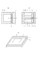
図1は、第一の実施形態の光電変換装置を示す。図1(c)は光電変換装置の斜視図であり、図1(a)および図1(b)は、図1(c)の光電変換装置を光入射側から見た平面図である。 FIG. 1 shows a photoelectric conversion device of the first embodiment. FIG. 1(c) is a perspective view of the photoelectric conversion device, and FIGS. 1(a) and 1(b) are plan views of the photoelectric conversion device of FIG. 1(c) viewed from the light incident side.
本実施形態に係る光電変換装置は、図1(c)に示すように、第1基板2と第2基板5を貼り合わせた積層構造をとり、画素部1、パッド部4を有する。第1基板2と第2基板5との間には配線構造が配され、この配線構造は複数の配線層を含む。以下、添え字でA、Bが振られている場合には、第1基板2に配される構成にA、第2基板5に配される構成にBを振ることとする。第1基板2と第2基板5を貼り合わせた際にAとBは重なるように配置される。A、Bのそれぞれを付された素子同士は配線層を介して電気的に接続される。あるいは、A、Bのそれぞれを付された素子の一方を開口部として、他方に接続された配線を基板表面まで通してもよい。図1(c)に示す光電変換装置では、第一面を第1基板2の表面としたとき、対向する第二面が第2基板5の表面となる。
As shown in FIG. 1C, the photoelectric conversion device according to this embodiment has a laminated structure in which a
図1(a)に示すように、第1基板2は、画素部1A、放熱部3、基板の外周部に配されたパッド部4Aを有する。
As shown in FIG. 1A, the
また、図1(b)に示すように、第2基板5は、画素部1B、放熱部3、パッド部4B、垂直走査部6、接続部7、AD変換部8、信号処理部9、機械学習処理部10、出力インターフェース部11が配されている。本図では、AD変換部8、信号処理部9、機械学習処理部10、出力インターフェース部11は上下に2系統有する。本図では、AD変換部8から信号処理部9、機械学習処理部10、出力インターフェース部11へは1箇所で接続されるが、複数個所で接続することもできる。
Further, as shown in FIG. 1B, the
本図において、機械学習処理部10は2つに分割されるが、分割されていなくてもよい。あるいは、機能としては一体であるものを物理的に分割して配置してもよい。
Although the machine
放熱部3は、機械学習処理部10と近接する領域の少なくとも一部に形成される。機械学習処理部10と近接する領域とは、例えば機械学習処理部10と接する領域(複数に分割された機械学習処理部10の間の領域を含む)である。第1基板2の第2基板5と電気的に接続された領域のうち、第2基板5の機械学習処理部10と平面的に対応する領域や、平面視で対応する領域(上面からの射影のこと)と接する領域、半導体活性領域も含む。
The
パッド部4Aおよびパッド部4Bの少なくとも一方には、複数のパッド部4が配置されており、パッド部4は外部回路との信号などのやり取りを行う入力パッド、出力パッドを含む。また、パッド部4には、外部回路が電気的に接続される、配線層に配置された電極パッドや半導体基板の一方の面から対向する他方の面に貫通する貫通電極と接続される電極パッドが含まれる。図1(a)および図1(b)には、基板の外周部4辺にパッド部4を配置しているが、パッド部4の配置は、本構成に限られず変更可能である。
A plurality of pad sections 4 are arranged in at least one of the
接合部7は第1基板2と第2基板5とを電気的に接続する金属接続(メタルボンディング)やTSV(Through-Silicon Via)構造である。
The
図2は、第一の実施形態における光電変換装置の全体構成を示す図である。光電変換装置は、図2に示されるように、画素部1、垂直走査部6、AD変換部8、信号処理部9、機械学習処理部10、出力インターフェース部11を含んで構成されている。本図では、図1にて上下に2系統有する要素についても下に1つのみ示す。また、接続部7は図2では図示を省略する。
FIG. 2 is a diagram showing the overall configuration of the photoelectric conversion device according to the first embodiment. The photoelectric conversion device includes a
画素部1は、水平、垂直方向に複数の受光画素12を含む。受光画素12のそれぞれは外部から入射する光を光電変換し、入射光量に応じた電荷を生成する。画素部1の各行には共通の画素駆動信号線13が接続され、画素部1の受光画素12は垂直走査部6より画素駆動信号線13に供給された制御パルスにより駆動されている。また、画素部1の各列には共通の垂直出力線14が接続され、これらの画素で生じる電荷を画素信号として出力している。各列の垂直出力線14に出力された受光画素12の画素信号は、各列に配されたAD変換部8に入力される。
The
なお、画素部1を構成する画素の数は、特に限定されるものではない。例えば、一般的なデジタルカメラのように数千行×数千列の画素で画素部1を構成してもよく、1行又は1列に並べた複数の画素で画素部1を構成してもよい。
The number of pixels forming the
AD変換部8では入力された画素信号の増幅およびAD変換が行われ、出力データは信号処理部9に入力される。
The
信号処理部9では、AD変換部8の出力データに対して信号処理が行われる。この信号処理は、CDS(Correlated Double Sampling)のほか、オフセット除去など、画像処理の一部に相当する処理が行われてもよい。また、信号処理部9の一部、あるいは全部と機械学習処理部10の機能を統合して機械学習処理部10として形成することも可能である。
The
信号処理部9から出力されたデータは機械学習処理部10に入力され、機械学習によって作成された学習済みモデルを用いた各種処理が実行される。
Data output from the
学習済みモデルは、例えば、ディープニューラルネットワーク(DNN)を利用した機械学習によって作成される。このような学習済みモデルをニューラルネットワーク計算モデルともいう。 A trained model is created, for example, by machine learning using a deep neural network (DNN). Such a trained model is also called a neural network calculation model.
この学習済みモデルは、画素部1からの出力に相当する入力信号と、この入力信号に対するラベルとが紐付いている学習データとを所定の機械学習モデルに入力して生成されたパラメータに基づいて設計されていてもよい。また、所定の機械学習モデルは、多層のニューラルネットワークを利用した機械学習モデルであってもよい。このような学習済みモデルを多層ニューラルネットワークモデルともいう。
This trained model is designed based on parameters generated by inputting an input signal corresponding to the output from the
処理後のデータは、出力インターフェース部11を介して出力される。
The processed data is output via the
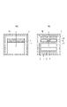
図3は、図1のX-X’線での断面模式図である。第1基板2の画素部1A、放熱部3、パッド部4Aとこれらに対応する第2基板5の構造を示している。第1基板2および第2基板5は、複数の配線層が絶縁膜を介して積層された構造を有している。放熱部3は第1基板2および第2基板5を含む領域である。
FIG. 3 is a schematic cross-sectional view taken along line X-X' of FIG. The structure of a
第1基板2の光入射側に配される半導体基板301は、素子領域308を有し、素子領域308は素子分離領域309で分離される。
A
層間絶縁膜302は、主に絶縁材料(半導体基板としてシリコンを用いる場合、シリコン酸化物)からなり、ゲート電極やゲート配線を含むゲート電極層310、配線層312、素子領域308と配線層312を接続するプラグ層311を含む。
The
第1基板2と第2基板5が物理的に接合される面である基板接合部306では、接合部7である金属接続(メタルボンディング)により第1基板2と第2基板が電気的に接続される。
The
層間絶縁膜302と基板接合部306の間には、複数の層間絶縁膜303、304、305が積層されている。層間絶縁膜303は、配線層314と配線層間を接続するプラグ層313を含む。層間絶縁膜304も同様に配線層間を接続するプラグ層を含む構成となっている。層間絶縁膜305は、配線層とプラグ層に加え、機械学習処理部10で発生した熱を放熱するための放熱パッド322を有する。放熱パッド322は、層間絶縁膜305に含まれる配線層と同一層で形成される導電パターンにより構成することができる。
A plurality of interlayer insulating
第2基板5に配される半導体基板315は素子領域320を含む。素子領域320は素子分離領域321で分離される。
A
層間絶縁膜316は、層間絶縁膜302と同様にゲート電極層、配線層、プラグ層を含む。層間絶縁膜316と、第1基板2と第2基板5の基板接合部306の間には、複数の層間絶縁膜317、318、319が積層されている。層間絶縁膜317、318には、層間絶縁膜303、304と同様に配線層とプラグ層が含まれ、層間絶縁膜319は、層間絶縁膜305と同様に配線層、プラグ層および放熱パッド323を有する。放熱パッド323は、放熱パッド322と同様に層間絶縁膜319に含まれる配線層と同一層で形成される導電パターンにより構成される。放熱パッド323と放熱パッド322は、基板接合部306で接合されている。
The
画素部1Aの素子領域308には、画素を構成するトランジスタやフォトダイオードが配され、放熱部3の素子領域308には、容量を構成する構造が配される。素子領域308はウエルの電位供給用の領域としても用いられる。あるいは、素子領域308には電位が与えられなくてもよい。
The
画素部1の光入射側には、光を集光させるマイクロレンズ307が配され、放熱部3の光入射側には放熱構造324が配される。放熱構造324は、例えば、微細加工技術によって形成されたMEMS(Micro Electro Mechanical Systems)などであり、第1基板2の少なくとも一部の表面の、画素領域以外の領域に貼り付けられる。
A
機械学習処理部10で発生した熱は、機械学習処理部10と近接する領域の素子を経由して伝導する。例えば、半導体基板としてシリコンを用いる場合、素子分離領域となるシリコン酸化物の熱伝導率(約1.4(W/m・K))は素子領域(シリコン)の熱伝導率(約150(W/m・K))に対して2桁以上小さい。そのため、素子ではない場所を素子分離領域であるシリコン酸化物ではなく素子領域と同じシリコンで形成することで熱伝導が大きい箇所を増やすことができ、放熱を促進することが可能である。この場合、素子間の分離はPN分離を用いてもよい。
The heat generated by the machine
また、機械学習処理部10で発生した熱は、機械学習処理部10と近接する領域のポリシリコンを経由しても伝導する。ポリシリコンの熱伝導率はシリコンと略同等であり、素子ではない場所をポリシリコンで形成することでも熱伝導が大きい箇所を増やすことができ、放熱を促進することが可能である。このとき、ポリシリコンをメッシュ状のパターンとすることで、より高い効率で放熱を促進することが可能である。
Moreover, the heat generated by the machine
第2基板5の配線層およびプラグ層を介して放熱パッド323に伝搬された熱は、第1基板2の層間絶縁膜305に配される放熱パッド322およびプラグ層を介して、層間絶縁膜304に含まれる配線層に伝搬される。前記配線層は、パッド部4Aに接続されており、パッド部4Aを介して放熱される。このように、機械学習部10が配される第2基板5と第1基板2が電気的に接続された箇所から放熱されるため、機械学習部10で発生した熱を効率よく放熱することができる。放熱経路となる配線層や放熱パッドをメッシュ状のパターンとすることで、より高い効率で放熱を促進することが可能である。
The heat propagated to the
また、第2基板5の配線層およびプラグ層を介して放熱パッド323に伝搬された熱は、第1基板2の層間絶縁膜305に配される放熱パッド322および第1基板2に形成されるTSV構造325を介して、第1基板2の表面などからも放熱される。本実施例では、TSV構造325は放熱構造324に接続されているため、機械学習部10で発生した熱を放熱構造324を介して高効率で放熱することができる。また、TSV構造325をメッシュ状のパターンとすることで、より高い効率で放熱を促進することが可能である。メッシュ状の配置とは、具体的にはTSV構造をマトリックス状に配置してもよく、マトリックス状に配置したTSV構造同士を配線で接続してもよい。また、二次元上の網目構造に限られず、例えばTSV構造同士を縦横に接続し、三次元に網目状の構造を構成してもよい。
Further, the heat propagated to the
なお、図3のパッド部4Aは層間絶縁膜304までが開口され、開口部に配された電極パッドが配線層を介してパッド部4Bと電気的に接続されるが、パッド部4の構成はこれに限られない。たとえばパッド部4Aを相関絶縁膜318までの開口部とし、パッド部4Bに電極パッドを配してもよい。
Note that the
(第一の実施形態の変形例1)
図4は、第一の実施形態に係る光電変換装置の変形例の概略図である。図3のTSV構造325が空洞構造326に変わっている。空洞構造326は、TSV構造325同様に機械学習処理部10から伝搬された熱を放熱する。
(
FIG. 4 is a schematic diagram of a modification of the photoelectric conversion device according to the first embodiment.
空洞構造326はパッド部4Aと同様に形成される。外部回路との信号などのやり取りを行わない場合、外部回路との接続のためのワイヤーボンディングが不要であり、空洞サイズを小さくすることが可能である。そのため、複数の空洞構造を形成し、チップ外との接触界面面積を増加させることで高い放熱効果を得ることも可能である。また、空洞構造をメッシュ状のパターンとすることで、より高い効率で放熱を促進することが可能である。
The
(第一の実施形態の変形例2)
図5は、第一の実施形態に係る光電変換装置の変形例の概略図である。図3の第1基板2に形成されるTSV構造325がなく、第2基板5にTSV構造327が形成される。
(
FIG. 5 is a schematic diagram of a modification of the photoelectric conversion device according to the first embodiment. A
TSV構造327は第2基板5の表面に露出され、第2基板の配線層およびプラグ層を介して放熱パッド323に伝搬された熱は、TSV構造327を介して、第2基板5の表面から放熱される。第2基板5の表面は、パッケージとの接触面になるため、より高い放熱効果を得ることができる。図5に示す構成では、発熱箇所である機械学習処理部10に近い箇所から放熱することも可能であり、その場合、より高い放熱効果を得ることができる。
The
(第一の実施形態の変形例3)
図6は、第一の実施形態に係る光電変換装置の変形例の概略図である。図5のTSV構造327が空洞構造328に変わっている。
(
FIG. 6 is a schematic diagram of a modification of the photoelectric conversion device according to the first embodiment. The
空洞構造328は、空洞構造326と異なり放熱構造形成のためのプロセスが必要である。第1基板2とは異なり、第2基板5の表面には画素がないため空洞328は配置面積の制限が少なく、多くの空洞構造を形成することが可能である。また、発熱箇所である機械学習処理部10に近い箇所から放熱することも可能であることと併せ、より高い放熱効果を得ることができる。
The
(第一の実施形態の変形例4)
図7は、第一の実施形態に係る光電変換装置の変形例の概略図である。図6の放熱パッド323、放熱パッド322および、放熱パッド322に接続される第1基板2の配線層およびプラグ層、ポリシリコンがない。つまり、放熱構造が第1基板に接する領域を有さず、第2基板5の表面から放熱する。
(Modification 4 of the first embodiment)
FIG. 7 is a schematic diagram of a modification of the photoelectric conversion device according to the first embodiment. There are no
このため、特に画素周辺部が小さくチップ面積のうち画素領域が占める割合が大きいチップの場合には、画素近傍が放熱経路とならず、画素への影響を抑制することができる。 Therefore, especially in the case of a chip having a small pixel peripheral portion and a large proportion of the chip area occupied by the pixel region, the vicinity of the pixel does not serve as a heat dissipation path, and the influence on the pixel can be suppressed.
(第一の実施形態の変形例5)
図8は、第一の実施形態に係る光電変換装置の変形例の概略図である。図7に対して第1基板2と第2基板5との間に第3基板800が貼り合わされる。
(
FIG. 8 is a schematic diagram of a modification of the photoelectric conversion device according to the first embodiment. A
第1基板2、は基板接合部802で、第2基板5は基板接合部803で、それぞれ金属接合部によって第3基板800と接合される。基板接合部802、基板接合部803間はビア801によって接続される。ビア801にはTSVなどが用いられる。第1基板2、第2基板5のそれぞれと第3基板800の接続は本図では省略する。第3基板800には、例えばSRAMなどが配置される。
The
第3基板800として、MEMSなどによる放熱構造を貼り合わせることもできる。他の基板が放熱構造である場合、第2基板5が放熱パッド323、および、放熱パッド322を介して第3基板800と電気的に接続されることで、高い放熱効果を得ることができる。
As the
また、本変形例では第1基板2と第2基板5との間に第3基板800が配されたが、第2基板5の第1基板2と接合される面を第三面としたときに、第三面に対向する第2基板5の第四面側にさらに第4基板804が配されてもかまわない。
Further, in this modified example, the
(第一の実施形態の変形例6)
図1に示す配置の他にも、光電変換装置の要素配置が考えられる。光電変換装置の要素配置の一例として図9のような構成がある。図1ではAD変換部8、信号処理部9を上下に2系統有するが、図9では1系統のみである。
(
In addition to the arrangement shown in FIG. 1, other element arrangements of the photoelectric conversion device are conceivable. FIG. 9 shows an example of arrangement of elements in a photoelectric conversion device. In FIG. 1, there are two systems of the
(第二の実施形態)
本発明の第二の実施形態について図10及び図11を用いて説明する。第一の実施形態と共通する構成についての詳細な説明は省略し、主に第一の実施形態と異なる点について説明する。
(Second embodiment)
A second embodiment of the present invention will be described with reference to FIGS. 10 and 11. FIG. A detailed description of the configuration common to the first embodiment will be omitted, and differences from the first embodiment will be mainly described.
図10は、第二の実施形態の光電変換装置を示している。光電変換装置の斜視図は、図1(c)と同様である。図10(a)および図10(b)は、光電変換装置を光入射側から見た平面図である。 FIG. 10 shows the photoelectric conversion device of the second embodiment. A perspective view of the photoelectric conversion device is the same as FIG. 1(c). 10(a) and 10(b) are plan views of the photoelectric conversion device viewed from the light incident side.
図10(b)に示すように、第2基板5は、画素部1B、放熱部3、パッド部4B、垂直走査部6、接続部7、AD変換部8、信号処理部9、出力インターフェース部11が配されている。
As shown in FIG. 10B, the
本図では、AD変換部8、信号処理部9、出力インターフェース部11は上下に2系統有する。また、基板の外周部にパッド部4Bが配されている。本実施例では出力インターフェース部11が高速動作するために発熱が大きいことを想定しており、出力インターフェース部11と近接する領域に放熱部3が形成されるが、他の領域でもよい。
In the figure, the
図11は、第二の実施形態における光電変換装置の全体構成を示す図である。光電変換装置は、図11に示されるように、画素部1、垂直走査部6、AD変換部8、信号処理部9、出力インターフェース部11を含んで構成されている。本図では、図1にて上下に2系統有する要素についても下に1つのみ示す。また、接続部7は省略する。
FIG. 11 is a diagram showing the overall configuration of a photoelectric conversion device according to the second embodiment. The photoelectric conversion device includes a
なお、本光電変換装置に機械学習処理部を追加することも可能である。 It is also possible to add a machine learning processing unit to this photoelectric conversion device.
本実施形態に対応する図10のX-X’線での断面模式図は図8と同じである。 The schematic cross-sectional view taken along line X-X' in FIG. 10 corresponding to this embodiment is the same as FIG.
本実施形態では、第1基板2、第2基板5の間に張り合わされる第3基板800がMEMSによる放熱構造である。放熱効果の高いマイクロ流体構造を放熱構造として適用可能である。第1基板2、第2基板5の間に特に放熱効果の大きい第3基板800を貼り付けることで、出力インターフェース部11が配された第2基板5から第1基板2への熱の伝搬を抑制することができる。
In this embodiment, the
(第三の実施形態)
第三の実施形態について説明する。
(Third embodiment)
A third embodiment will be described.
第三の実施形態の光電変換装置も図10、11で示される。第一及び第二の実施形態と共通する構成についての詳細な説明は省略し、主に第一の実施形態と異なる点について説明する。 A photoelectric conversion device of the third embodiment is also shown in FIGS. A detailed description of the configuration common to the first and second embodiments will be omitted, and differences from the first embodiment will be mainly described.
本実施形態に対応する図10のX-X’線での断面模式図は図8と同じである。 The schematic cross-sectional view taken along line X-X' in FIG. 10 corresponding to this embodiment is the same as FIG.
本実施形態では、第1基板2、第2基板5の間に張り合わされる第3基板800に、例えばSRAMなどが配置される。第1基板2、第2基板5のそれぞれと第3基板800の接続は本図では省略する。この場合、放熱構造が第1基板に接する領域を有さず、第2基板5の表面から放熱するため、特に画素周辺部が小さくチップ面積のうち画素領域が占める割合が大きいチップである場合には、画素近傍が放熱経路とならず、画素への影響を抑制することができる。
In this embodiment, for example, an SRAM or the like is arranged on the
また、本実施例では、第1基板2、第2基板5の間に張り合わされる第3基板800がMEMSによる放熱構造であってもよい。このように、第1基板2、第2基板5の間に放熱効果の大きい第3基板800を貼り付けることで、出力インターフェース部11が配された第2基板5から第1基板2への熱の伝搬を抑制することができる。
Further, in this embodiment, the
(第四の実施形態)
図12は、本実施形態に係る光電変換システム11200の構成を示すブロック図である。本実施形態の光電変換システム11200は、光電変換装置11204を含む。ここで、光電変換装置11204は、上述の実施形態で述べた光電変換装置のいずれかを適用することができる。光電変換システム11200は例えば、撮像システムとして用いることができる。撮像システムの具体例としては、デジタルスチルカメラ、デジタルカムコーダー、監視カメラ、ネットワークカメラ、顕微鏡等が挙げられる。図12では、光電変換システム11200としてデジタルスチルカメラの例を示している。
(Fourth embodiment)
FIG. 12 is a block diagram showing the configuration of a
図12に示す光電変換システム11200は、光電変換装置11204、被写体の光学像を光電変換装置11204に結像させるレンズ11202を有する。また、光電変換システム11200はレンズ11202を通過する光量を可変にするための絞り11203、レンズ11202の保護のためのバリア11201を有する。レンズ11202および絞り11203は、光電変換装置11204に光を集光する光学系である。
A
光電変換システム11200は、光電変換装置11204から出力される出力信号の処理を行う信号処理部11205を有する。信号処理部11205は、必要に応じて入力信号に対して各種の補正、圧縮を行って出力する信号処理の動作を行う。光電変換システム11200は、更に、画像データを一時的に記憶するためのバッファメモリ部11206、外部コンピュータ等と通信するための外部インターフェース部(外部I/F部)11209を有する。更に光電変換システム11200は、撮像データの記録または読み出しを行うための半導体メモリ等の記録媒体11211、記録媒体11211に記録または読み出しを行うための記録媒体制御インターフェース部(記録媒体制御I/F部)11210を有する。記録媒体11211は、光電変換システム11200に内蔵されていてもよく、着脱可能であってもよい。また、記録媒体制御I/F部11210から記録媒体11211との通信や外部I/F部11209からの通信は無線によってなされてもよい。
The
更に光電変換システム11200は、各種演算を行うとともにデジタルスチルカメラ全体を制御する全体制御・演算部11208、光電変換装置11204と信号処理部11205に各種タイミング信号を出力するタイミング発生部11207を有する。ここで、タイミング信号などは外部から入力されてもよく、光電変換システム11200は、少なくとも光電変換装置11204と、光電変換装置11204から出力された出力信号を処理する信号処理部11205とを有すればよい。全体制御・演算部11208およびタイミング発生部11207は、光電変換装置11204の制御機能の一部または全部を実施するように構成してもよい。
Further, the
光電変換装置11204は、画像用信号を信号処理部11205に出力する。信号処理部11205は、光電変換装置11204から出力される画像用信号に対して所定の信号処理を実施し、画像データを出力する。また、信号処理部11205は、画像用信号を用いて、画像を生成する。また、信号処理部11205は、光電変換装置11204から出力される信号に対して測距演算を行ってもよい。なお、信号処理部11205やタイミング発生部11207は、光電変換装置に搭載されていてもよい。つまり、信号処理部11205やタイミング発生部11207は、画素が配された基板に設けられていてもよいし、別の基板に設けられている構成であってもよい。上述した各実施形態の光電変換装置を用いて撮像システムを構成することにより、より良質の画像が取得可能な撮像システムを実現することができる。
The
(第五の実施形態)
図13は、前述の実施形態に記載の光電変換装置を利用した電子機器である距離画像センサの構成例を示すブロック図である。
(Fifth embodiment)
FIG. 13 is a block diagram showing a configuration example of a distance image sensor, which is an electronic device using the photoelectric conversion device described in the above embodiments.
図13に示すように、距離画像センサ12401は、光学系12407、光電変換装置12408、画像処理回路12404、モニタ12405、およびメモリ12406を備えて構成される。そして、距離画像センサ12401は、光源装置12409から被写体に向かって投光され、被写体の表面で反射された光(変調光やパルス光)を受光することにより、被写体までの距離に応じた距離画像を取得することができる。
As shown in FIG. 13, the
光学系12407は、1枚または複数枚のレンズを有して構成され、被写体からの像光(入射光)を光電変換装置12408に導き、光電変換装置12408の受光面(センサ部)に結像させる。 The optical system 12407 includes one or more lenses, guides image light (incident light) from a subject to the photoelectric conversion device 12408, and forms an image on the light receiving surface (sensor portion) of the photoelectric conversion device 12408. Let
光電変換装置12408としては、上述した各実施形態の光電変換装置が適用され、光電変換装置12408から出力される受光信号から求められる距離を示す距離信号が画像処理回路12404に供給される。
As the photoelectric conversion device 12408 , the photoelectric conversion device of each of the embodiments described above is applied, and a distance signal indicating the distance obtained from the received light signal output from the photoelectric conversion device 12408 is supplied to the
画像処理回路12404は、光電変換装置12408から供給された距離信号に基づいて距離画像を構築する画像処理を行う。そして、その画像処理により得られた距離画像(画像データ)は、モニタ12405に供給されて表示されたり、メモリ406に供給されて記憶(記録)されたりする。
The
このように構成されている距離画像センサ12401では、上述した光電変換装置を適用することで、画素の特性向上に伴って、例えば、より正確な距離画像を取得することができる。
In the
(第六の実施形態)
本開示に係る技術(本技術)は、様々な製品へ応用することができる。例えば、本開示に係る技術は、内視鏡手術システムに適用されてもよい。
(Sixth embodiment)
The technology (the present technology) according to the present disclosure can be applied to various products. For example, the technology according to the present disclosure may be applied to an endoscopic surgery system.
図14は、本開示に係る技術(本技術)が適用され得る内視鏡手術システムの概略的な構成の一例を示す図である。 FIG. 14 is a diagram showing an example of a schematic configuration of an endoscopic surgery system to which the technique (the present technique) according to the present disclosure can be applied.
図14では、術者(医師)13131が、内視鏡手術システム13003を用いて、患者ベッド13133上の患者13132に手術を行っている様子が図示されている。図示するように、内視鏡手術システム13003は、内視鏡13100と、術具13110と、内視鏡下手術のための各種の装置が搭載されたカート13134と、から構成される。
FIG. 14 shows an operator (physician) 13131 performing surgery on a
内視鏡13100は、先端から所定の長さの領域が患者13132の体腔内に挿入される鏡筒13101と、鏡筒13101の基端に接続されるカメラヘッド13102と、から構成される。図示する例では、硬性の鏡筒13101を有するいわゆる硬性鏡として構成される内視鏡13100を図示しているが、内視鏡13100は、軟性の鏡筒を有するいわゆる軟性鏡として構成されてもよい。
An
鏡筒13101の先端には、対物レンズが嵌め込まれた開口部が設けられている。内視鏡13100には光源装置13203が接続されており、光源装置13203によって生成された光が、鏡筒13101の内部に延設されるライトガイドによって当該鏡筒の先端まで導光される。この光は対物レンズを介して患者13132の体腔内の観察対象に向かって照射される。なお、内視鏡13100は、直視鏡であってもよいし、斜視鏡又は側視鏡であってもよい。
The tip of the lens barrel 13101 is provided with an opening into which an objective lens is fitted. A
カメラヘッド13102の内部には光学系及び光電変換装置が設けられており、観察対象からの反射光(観察光)は当該光学系によって当該光電変換装置に集光される。当該光電変換装置によって観察光が光電変換され、観察光に対応する電気信号、すなわち観察像に対応する画像信号が生成される。当該光電変換装置としては、前述の各実施形態に記載の光電変換装置を用いることができる。当該画像信号は、RAWデータとしてカメラコントロールユニット(CCU:Camera Control Unit)13135に送信される。
An optical system and a photoelectric conversion device are provided inside the
CCU13135は、CPU(Central Processing Unit)やGPU(Graphics Processing Unit)等によって構成され、内視鏡13100及び表示装置13136の動作を統括的に制御する。さらに、CCU13135は、カメラヘッド13102から画像信号を受け取り、その画像信号に対して、例えば現像処理(デモザイク処理)等の、当該画像信号に基づく画像を表示するための各種の画像処理を施す。
The
表示装置13136は、CCU13135からの制御により、当該CCU13135によって画像処理が施された画像信号に基づく画像を表示する。
The
光源装置13203は、例えばLED(Light Emitting Diode)等の光源から構成され、術部等を撮影する際の照射光を内視鏡13100に供給する。
The
入力装置13137は、内視鏡手術システム13003に対する入力インターフェースである。ユーザは、入力装置13137を介して、内視鏡手術システム13003に対して各種の情報の入力や指示入力を行うことができる。
An
処置具制御装置13138は、組織の焼灼、切開又は血管の封止等のためのエネルギー処置具13112の駆動を制御する。
The treatment
内視鏡13100に術部を撮影する際の照射光を供給する光源装置13203は、例えばLED、レーザ光源又はこれらの組み合わせによって構成される白色光源から構成することができる。RGBレーザ光源の組み合わせにより白色光源が構成される場合には、各色(各波長)の出力強度及び出力タイミングを高精度に制御することができるため、光源装置13203において撮像画像のホワイトバランスの調整を行うことができる。また、この場合には、RGBレーザ光源それぞれからのレーザ光を時分割で観察対象に照射し、その照射タイミングに同期してカメラヘッド13102の撮像素子の駆動を制御することにより、RGBそれぞれに対応した画像を時分割で撮像することも可能である。当該方法によれば、当該撮像素子にカラーフィルタを設けなくても、カラー画像を得ることができる。
The
また、光源装置13203は、出力する光の強度を所定の時間ごとに変更するようにその駆動が制御されてもよい。その光の強度の変更のタイミングに同期してカメラヘッド13102の撮像素子の駆動を制御して時分割で画像を取得し、その画像を合成することにより、いわゆる黒つぶれ及び白とびのない高ダイナミックレンジの画像を生成することができる。
Further, the driving of the
また、光源装置13203は、特殊光観察に対応した所定の波長帯域の光を供給可能に構成されてもよい。特殊光観察では、例えば、体組織における光の吸収の波長依存性を利用する。具体的には、通常の観察時における照射光(すなわち、白色光)に比べて狭帯域の光を照射することにより、粘膜表層の血管等の所定の組織を高コントラストで撮影する。あるいは、特殊光観察では、励起光を照射することにより発生する蛍光により画像を得る蛍光観察が行われてもよい。蛍光観察では、体組織に励起光を照射し当該体組織からの蛍光を観察すること、又はインドシアニングリーン(ICG)等の試薬を体組織に局注するとともに当該体組織にその試薬の蛍光波長に対応した励起光を照射し蛍光像を得ること等を行うことができる。光源装置13203は、このような特殊光観察に対応した狭帯域光及び/又は励起光を供給可能に構成され得る。
Also, the
(第七の実施形態)
本実施形態の光電変換システムおよび移動体について、図15及び図16を用いて説明する。図15は、本実施形態による光電変換システムおよび移動体の構成例を示す概略図である。本実施形態では、光電変換システムとして、車載カメラの一例を示す。
(Seventh embodiment)
A photoelectric conversion system and a moving object according to this embodiment will be described with reference to FIGS. 15 and 16. FIG. FIG. 15 is a schematic diagram showing a configuration example of a photoelectric conversion system and a moving object according to this embodiment. In this embodiment, an example of an in-vehicle camera is shown as a photoelectric conversion system.
図15は、車両システムとこれに搭載される撮像を行う光電変換システムの一例を示したものである。光電変換システム14301は、光電変換装置14302、画像前処理部14315、集積回路14303、光学系14314を含む。光学系14314は、光電変換装置14302に被写体の光学像を結像する。光電変換装置14302は、光学系14314により結像された被写体の光学像を電気信号に変換する。光電変換装置14302は、上述の各実施形態のいずれかの光電変換装置である。画像前処理部14315は、光電変換装置14302から出力された信号に対して所定の信号処理を行う。画像前処理部14315の機能は、光電変換装置14302内に組み込まれていてもよい。光電変換システム14301には、光学系14314、光電変換装置14302および画像前処理部14315が、少なくとも2組設けられており、各組の画像前処理部14315からの出力が集積回路14303に入力されるようになっている。
FIG. 15 shows an example of a vehicle system and a photoelectric conversion system mounted therein for imaging. A
集積回路14303は、撮像システム用途向けの集積回路であり、メモリ14305を含む画像処理部14304、光学測距部14306、測距演算部14307、物体認知部14308、異常検出部14309を含む。画像処理部14304は、画像前処理部14315の出力信号に対して、現像処理やキズ補正等の画像処理を行う。メモリ14305は、撮像画像の一次記憶、撮像画素のキズ位置を格納する。光学測距部14306は、被写体の合焦や、測距を行う。測距演算部14307は、複数の光電変換装置14302により取得された複数の画像データから測距情報の算出を行う。物体認知部14308は、車、道、標識、人等の被写体の認知を行う。異常検出部14309は、光電変換装置14302の異常を検出すると、主制御部14313に異常を発報する。
The
集積回路14303は、専用に設計されたハードウェアによって実現されてもよいし、ソフトウェアモジュールによって実現されてもよいし、これらの組合せによって実現されてもよい。また、FPGA(Field Programmable Gate Array)やASIC(Application Specific Integrated Circuit)等によって実現されてもよいし、これらの組合せによって実現されてもよい。
The
主制御部14313は、光電変換システム14301、車両センサ14310、制御ユニット14320等の動作を統括・制御する。主制御部14313を持たず、光電変換システム14301、車両センサ14310、制御ユニット14320が個別に通信インターフェースを有して、それぞれが通信ネットワークを介して制御信号の送受を行う(例えばCAN規格)方法も取り得る。
The
集積回路14303は、主制御部14313からの制御信号を受け或いは自身の制御部によって、光電変換装置14302へ制御信号や設定値を送信する機能を有する。
The
光電変換システム14301は、車両センサ14310に接続されており、車速、ヨーレート、舵角などの自車両走行状態および自車外環境や他車・障害物の状態を検出することができる。車両センサ14310は、対象物までの距離情報を取得する距離情報取得手段でもある。また、光電変換システム14301は、自動操舵、自動巡行、衝突防止機能等の種々の運転支援を行う運転支援制御部1311に接続されている。特に、衝突判定機能に関しては、光電変換システム14301や車両センサ14310の検出結果を基に他車・障害物との衝突推定・衝突有無を判定する。これにより、衝突が推定される場合の回避制御、衝突時の保安装置起動を行う。
The
また、光電変換システム14301は、衝突判定部での判定結果に基づいて、ドライバーに警報を発する警報装置14312にも接続されている。例えば、衝突判定部の判定結果として衝突可能性が高い場合、主制御部14313は、ブレーキをかける、アクセルを戻す、エンジン出力を抑制するなどして、衝突を回避、被害を軽減する車両制御を行う。警報装置14312は、音等の警報を鳴らす、カーナビゲーションシステムやメーターパネルなどの表示部画面に警報情報を表示する、シートベルトやステアリングに振動を与えるなどしてユーザに警告を行う。
The
本実施形態では、車両の周囲、例えば前方または後方を光電変換システム14301で撮影する。図15(b)に、車両前方を光電変換システム14301で撮像する場合の光電変換システム14301の配置例を示す。
In this embodiment, the
2つの光電変換装置14302は、車両14300の前方に配される。具体的には、車両14300の進退方位または外形(例えば車幅)に対する中心線を対称軸に見立て、その対称軸に対して2つの光電変換装置1302が線対称に配される。この形態は、車両14300と被写対象物との間の距離情報の取得や衝突可能性の判定を行う上で好ましい。また、光電変換装置14302は、運転者が運転席から車両14300の外の状況を視認する際に運転者の視野を妨げない配置が好ましい。警報装置14312は、運転者の視野に入りやすい配置が好ましい。
Two
また、本実施形態では、他の車両と衝突しない制御を説明したが、他の車両に追従して自動運転する制御や、車線からはみ出さないように自動運転する制御などにも適用可能である。さらに、光電変換システム14301は、自車両等の車両に限らず、例えば、船舶、航空機或いは産業用ロボットなどの移動体(移動装置)に適用することができる。加えて、移動体に限らず、高度道路交通システム(ITS)等、広く物体認識を利用する機器に適用することができる。
In addition, in the present embodiment, the control that does not collide with another vehicle has been described, but it is also applicable to control that automatically drives following another vehicle, control that automatically drives so as not to stray from the lane, and the like. . Furthermore, the
本発明の光電変換装置は、更に、距離情報など各種情報を取得可能な構成であってもよい。 The photoelectric conversion device of the present invention may further have a configuration capable of acquiring various information such as distance information.
(第八の実施形態)
図16は、1つの適用例に係る眼鏡16600(スマートグラス)を説明する。眼鏡16600には、光電変換装置16602を有する。光電変換装置16602は、上記の各実施形態に記載の光電変換装置である。また、レンズ16601の裏面側には、OLEDやLED等の発光装置を含む表示装置が設けられていてもよい。光電変換装置16602は1つでもよいし、複数でもよい。また、複数種類の光電変換装置を組み合わせて用いてもよい。光電変換装置16602の配置位置は図13(a)に限定されない。
(Eighth embodiment)
FIG. 16 illustrates glasses 16600 (smart glasses) according to one application.
眼鏡16600は、制御装置16603をさらに備える。制御装置16603は、光電変換装置16602と上記の表示装置に電力を供給する電源として機能する。また、制御装置16603は、光電変換装置16602と表示装置の動作を制御する。レンズ16601には、光電変換装置16602に光を集光するための光学系が形成されている。
図16(b)は、1つの適用例に係る眼鏡16610(スマートグラス)を説明する。眼鏡16610は、制御装置16612を有しており、制御装置16612に、光電変換装置16602に相当する光電変換装置と、表示装置が搭載される。レンズ16611には、制御装置16612内の光電変換装置と、表示装置からの発光を投影するための光学系が形成されており、レンズ16611には画像が投影される。制御装置16612は、光電変換装置および表示装置に電力を供給する電源として機能するとともに、光電変換装置および表示装置の動作を制御する。制御装置は、装着者の視線を検知する視線検知部を有してもよい。視線の検知は赤外線を用いてよい。赤外発光部は、表示画像を注視しているユーザの眼球に対して、赤外光を発する。発せられた赤外光の眼球からの反射光を、受光素子を有する撮像部が検出することで眼球の撮像画像が得られる。平面視における赤外発光部から表示部への光を低減する低減手段を有することで、画像品位の低下を低減する。
FIG. 16(b) illustrates glasses 16610 (smart glasses) according to one application. The
赤外光の撮像により得られた眼球の撮像画像から表示画像に対するユーザの視線を検出する。眼球の撮像画像を用いた視線検出には任意の公知の手法が適用できる。一例として、角膜での照射光の反射によるプルキニエ像に基づく視線検出方法を用いることができる。 The line of sight of the user with respect to the display image is detected from the captured image of the eye obtained by imaging the infrared light. Any known method can be applied to line-of-sight detection using captured images of eyeballs. As an example, it is possible to use a line-of-sight detection method based on a Purkinje image obtained by reflection of irradiation light on the cornea.
より具体的には、瞳孔角膜反射法に基づく視線検出処理が行われる。瞳孔角膜反射法を用いて、眼球の撮像画像に含まれる瞳孔の像とプルキニエ像とに基づいて、眼球の向き(回転角度)を表す視線ベクトルが算出されることにより、ユーザの視線が検出される。 More specifically, line-of-sight detection processing based on the pupillary corneal reflection method is performed. The user's line of sight is detected by calculating a line-of-sight vector representing the orientation (rotational angle) of the eyeball based on the pupil image and the Purkinje image included in the captured image of the eyeball using the pupillary corneal reflection method. be.
本実施形態の表示装置は、受光素子を有する光電変換装置を有し、光電変換装置からのユーザの視線情報に基づいて表示装置の表示画像を制御してよい。 The display device of the present embodiment may have a photoelectric conversion device having a light receiving element, and may control a display image of the display device based on the user's line-of-sight information from the photoelectric conversion device.
具体的には、表示装置は、視線情報に基づいて、ユーザが注視する第一の視界領域と、第一の視界領域以外の第二の視界領域とを決定される。第一の視界領域、第二の視界領域は、表示装置の制御装置が決定してもよいし、外部の制御装置が決定したものを受信してもよい。表示装置の表示領域において、第一の視界領域の表示解像度を第二の視界領域の表示解像度よりも高く制御してよい。つまり、第二の視界領域の解像度を第一の視界領域よりも低くしてよい。 Specifically, the display device determines a first visual field area that the user gazes at and a second visual field area other than the first visual field area, based on the line-of-sight information. The first viewing area and the second viewing area may be determined by the control device of the display device, or may be determined by an external control device. In the display area of the display device, the display resolution of the first viewing area may be controlled to be higher than the display resolution of the second viewing area. That is, the resolution of the second viewing area may be lower than that of the first viewing area.
また、表示領域は、第一の表示領域、第一の表示領域とは異なる第二の表示領域とを有し、視線情報に基づいて、第一の表示領域および第二の表示領域から優先度が高い領域を決定されてよい。第一の視界領域、第二の視界領域は、表示装置の制御装置が決定してもよいし、外部の制御装置が決定したものを受信してもよい。優先度の高い領域の解像度を、優先度が高い領域以外の領域の解像度よりも高く制御してよい。つまり優先度が相対的に低い領域の解像度を低くしてよい。 Further, the display area has a first display area and a second display area different from the first display area. may be determined. The first viewing area and the second viewing area may be determined by the control device of the display device, or may be determined by an external control device. The resolution of areas with high priority may be controlled to be higher than the resolution of areas other than areas with high priority. That is, the resolution of areas with relatively low priority may be lowered.
なお、第一の視界領域や優先度が高い領域の決定には、AIを用いてもよい。AIは、眼球の画像と当該画像の眼球が実際に視ていた方向とを教師データとして、眼球の画像から視線の角度、視線の先の目的物までの距離を推定するよう構成されたモデルであってよい。AIプログラムは、表示装置が有しても、光電変換装置が有しても、外部装置が有してもよい。外部装置が有する場合は、通信を介して、表示装置に伝えられる。 AI may be used to determine the first field of view area and the areas with high priority. The AI is a model configured to estimate the angle of the line of sight from the eyeball image and the distance to the object ahead of the line of sight, using the image of the eyeball and the direction in which the eyeball of the image was actually viewed as training data. It's okay. The AI program may be owned by the display device, the photoelectric conversion device, or the external device. If the external device has it, it is communicated to the display device via communication.
視認検知に基づいて表示制御する場合、外部を撮像する光電変換装置を更に有するスマートグラスに好ましく適用できる。スマートグラスは、撮像した外部情報をリアルタイムで表示することができる。 In the case of performing display control based on visual recognition detection, it can be preferably applied to smart glasses that further have a photoelectric conversion device that captures an image of the outside. Smart glasses can display captured external information in real time.
(第九の実施形態)
図17を参照しながら、本実施形態のシステムについて説明する。本実施形態は、医師等が患者から採取された細胞や組織を観察して病変を診断する病理診断システムやそれを支援する診断支援システムに適用することができる。本実施形態のシステムは、取得された画像に基づいて病変を診断又はその支援をしてもよい。
(Ninth embodiment)
The system of this embodiment will be described with reference to FIG. The present embodiment can be applied to a pathological diagnosis system in which a doctor or the like observes cells and tissues collected from a patient to diagnose a lesion, and a diagnosis support system that supports the system. The system of this embodiment may diagnose or assist in diagnosing lesions based on the acquired images.
図17に示すように、本実施形態のシステムは、1以上の病理システム15510を含む。さらに解析部15530と、医療情報システム15540とを含んでもよい。
As shown in FIG. 17, the system of this embodiment includes one or
1以上の病理システム15510それぞれは、主に病理医が使用するシステムであり、例えば研究所や病院に導入される。各病理システム15510は、互いに異なる病院に導入されてもよく、それぞれワイドエリアネットワークやローカルエリアネットワークなどの種々のネットワークを介して解析部15530及び医療情報システム15540に接続される。
Each of the one or
各病理システム15510は、顕微鏡15511と、サーバ15512と、表示装置15513とを含む。
Each
顕微鏡15511は、光学顕微鏡の機能を有し、ガラススライドに収められた観察対象物を撮像し、デジタル画像である病理画像を取得する。観察対象物とは、例えば、患者から採取された組織や細胞であり、臓器の肉片、唾液、血液等であってよい。
The
サーバ15512は、顕微鏡15511によって取得された病理画像を図示しない記憶部に記憶、保存する。また、サーバ15512は、閲覧要求を受け付けた場合に、メモリ等に保持された病理画像を検索し、検索された病理画像を表示装置15513に表示させることができる。サーバ15512と表示装置15513とは、表示を制御する装置等を介してもよい。
The
ここで、観察対象物が臓器の肉片等の固形物である場合、この観察対象物は、例えば、染色された薄切片であってよい。薄切片は、例えば、臓器等の検体から切出されたブロック片を薄切りすることで作製されてもよい。また、薄切りの際には、ブロック片がパラフィン等で固定されてもよい。 Here, when the observation object is a solid object such as a piece of flesh of an organ, the observation object may be, for example, a stained slice. A sliced piece may be produced, for example, by slicing a block piece excised from a specimen such as an organ. Also, when slicing, the block pieces may be fixed with paraffin or the like.
顕微鏡15511は、低解像度で撮像するための低解像度撮像部と、高解像度で撮像するための高解像度撮像部とを含み得る。低解像度撮像部と高解像度撮像部とは、異なる光学系であってもよいし、同一の光学系であってもよい。同一の光学系である場合には、顕微鏡15511は、撮像対象に応じて解像度が変更されてもよい。
The
観察対象物はガラススライドなどに収容され、顕微鏡15511の画角内に位置するステージ上に載置される。顕微鏡15511は、まず、低解像度撮像部を用いて画角内の全体画像を取得し、取得した全体画像から観察対象物の領域を特定する。続いて、顕微鏡15511は、観察対象物が存在する領域を所定サイズの複数の分割領域に分割し、各分割領域を高解像度撮像部により順次撮像することで、各分割領域の高解像度画像を取得する。対象とする分割領域の切替えでは、ステージを移動させてもよいし、撮像光学系を移動させてもよいし、それら両方を移動させてもよい。また、各分割領域は、ガラススライドの意図しない滑りによる撮像漏れ領域の発生等を防止するために、隣接する分割領域との間で重複していてもよい。さらに、全体画像には、全体画像と患者とを対応付けておくための識別情報が含まれていてもよい。この識別情報は、例えば、文字列やQRコード(登録商標)等であってよい。
The object to be observed is housed in a glass slide or the like and placed on a stage positioned within the angle of view of the
顕微鏡15511で取得された高解像度画像は、サーバ15512に入力される。サーバ15512は、各高解像度画像をより小さいサイズの部分画像に分割することができる。このように部分画像を生成すると、サーバ15512は、隣り合う所定数の部分画像を合成することで1つの画像を生成する合成処理を、全ての部分画像に対して実行する。この合成処理は、最終的に1つの部分画像が生成されるまで繰り返され得る。このような処理により、各階層が1つ以上の部分画像で構成されたピラミッド構造の部分画像群が生成される。このピラミッド構造では、ある層の部分画像とこの層とは異なる層の部分画像との画素数は同じであるが、その解像度が異なっている。例えば、2×2個の計4つの部分画像を合成して上層の1つの部分画像を生成する場合、上層の部分画像の解像度は、合成に用いた下層の部分画像の解像度の1/2倍となっている。
A high resolution image acquired by the
このようなピラミッド構造の部分画像群を構築することによって、表示対象のタイル画像が属する階層次第で、表示装置に表示される観察対象物の詳細度を切り替えることが可能となる。例えば、最下層の部分画像が用いられる場合には、観察対象物の狭い領域を詳細に表示し、上層の部分画像が用いられるほど観察対象物の広い領域が粗く表示されるようにすることができる。 By constructing such a pyramid-structured partial image group, it is possible to switch the level of detail of the observation object displayed on the display device, depending on the hierarchy to which the tile image to be displayed belongs. For example, when a partial image of the lowest layer is used, a narrow area of the observation object is displayed in detail, and as a partial image of the upper layer is used, a wide area of the observation object is displayed coarsely. can.
生成されたピラミッド構造の部分画像群は、例えば、メモリ等に記憶することができる。そして、サーバ15512は、他の装置(例えば、解析部15530)から識別情報を含む部分画像の取得要求を受け付けた場合に、識別情報に対応する部分画像を他の装置へ送信する。
The generated partial image group of the pyramid structure can be stored, for example, in a memory or the like. When the
なお、病理画像である部分画像は、焦点距離や染色条件等の撮像条件毎に生成されてもよい。撮像条件毎に部分画像が生成される場合、特定の病理画像とともに、特定の撮像条件と異なる撮像条件に対応する他の病理画像であって、特定の病理画像と同一領域の他の病理画像を並べて表示してもよい。特定の撮像条件は、閲覧者によって指定されてもよい。また、閲覧者に複数の撮像条件が指定された場合には、各撮像条件に対応する同一領域の病理画像が並べて表示されてもよい。 A partial image, which is a pathological image, may be generated for each imaging condition such as a focal length or staining condition. When partial images are generated for each imaging condition, a specific pathological image and other pathological images corresponding to imaging conditions different from the specific imaging condition and having the same region as the specific pathological image are generated. They may be displayed side by side. Specific imaging conditions may be specified by the viewer. Further, when a plurality of imaging conditions are specified by the viewer, pathological images of the same region corresponding to each imaging condition may be displayed side by side.
また、サーバ15512は、ピラミッド構造の部分画像群をサーバ15512以外の他の記憶装置、例えば、クラウドサーバ等に記憶してもよい。さらに、以上のような部分画像の生成処理の一部又は全部は、クラウドサーバ等で実行されてもよい。このように部分画像を使うことにより、ユーザは、観察倍率を変えながら観察対象物を観察しているような感覚を得ることができる。すなわち、表示を制御することにより、仮想顕微鏡のような役割を果たすことができる。ここでの仮想的な観察倍率は、実際には解像度に相当する。
The
医療情報システム15540は、いわゆる電子カルテシステムであり、患者を識別する情報、患者の疾患情報、診断に用いた検査情報や画像情報、診断結果、処方薬などの診断に関する情報を記憶する。例えば、ある患者の観察対象物を撮像することで得られる病理画像は、一旦、サーバ15512を介して保存された後、表示装置15514に表示され得る。病理システム15510を利用する病理医は、表示装置15513に表示された病理画像に基づいて病理診断を行う。病理医によって行われた病理診断結果は、医療情報システム15540に記憶される。
The
解析部15530は、病理画像に対する解析を実行し得る。この解析には、機械学習によって作成された学習モデルを用いることができる。解析部15530は、当該解析結果として、特定領域の分類結果や組織の識別結果等を導出してもよい。さらに、解析部15530は、細胞情報、数、位置、輝度情報等の識別結果やそれらに対するスコアリング情報等を導出してもよい。解析部15530で得られたこれらの情報は、診断支援情報として、病理システム15510の表示装置15513に表示されてもよい。
The
なお、解析部15530は、1台以上のサーバ(クラウドサーバを含む)等で構成されたサーバシステムであってもよい。また、解析部15530は、病理システム15510内の例えばサーバ15512に組み込まれた構成であってもよい。すなわち、病理画像に対する各種解析は、病理システム15510内で実行されてもよい。
Note that the
上述の実施形態で説明した光電変換装置は、以上説明した構成のうち、例えば、顕微鏡15511に好適に適用され得る。具体的には、顕微鏡15511における低解像度撮像部及び/ 又は高解像度撮像部に適用することができる。これにより、低解像度撮像部及び/ 又は高解像度撮像部の小型化、強いては、顕微鏡15511の小型化が可能となる。それにより、顕微鏡15511の運搬が容易となるため、システム導入やシステム組換え等を容易化することが可能となる。さらに、上述の実施形態で説明した光電変換装置を適用することにより、病理画像の取得から病理画像の解析までの処理の一部又は全部を顕微鏡15511内においてオンザフライで実行可能となるため、より迅速且つ的確な診断支援情報の出力も可能となる。
The photoelectric conversion device described in the above embodiments can be suitably applied to, for example, the
なお、上記で説明した構成は、診断支援システムに限らず、共焦点顕微鏡や蛍光顕微鏡、ビデオ顕微鏡等の生物顕微鏡全般にも適用され得る。ここで、観察対象物は、培養細胞や受精卵、精子等の生体試料、細胞シート、三次元細胞組織等の生体材料、ゼブラフィッシュやマウス等の生体であってもよい。また、観察対象物は、ガラススライドに限らず、ウェルプレートやシャーレ等に格納された状態で観察されることもできる。 The configuration described above can be applied not only to the diagnosis support system but also to general biological microscopes such as confocal microscopes, fluorescence microscopes, and video microscopes. Here, the object to be observed may be a biological sample such as cultured cells, fertilized eggs, or sperm, a biological material such as a cell sheet or a three-dimensional cell tissue, or a living body such as a zebrafish or mouse. Further, the object to be observed is not limited to a glass slide, and can be observed while stored in a well plate, petri dish, or the like.
さらに、顕微鏡を利用して取得した観察対象物の静止画像から動画像が生成されてもよい。例えば、所定期間連続的に撮像した静止画像から動画像を生成してもよいし、所定の間隔を空けて撮像した静止画像から画像シーケンスを生成してもよい。このように、静止画像から動画像を生成することで、がん細胞や神経細胞、心筋組織、精子等の拍動や伸長、遊走等の動きや培養細胞や受精卵の分裂過程など、観察対象物の動的な特徴を機械学習を用いて解析することが可能となる。 Furthermore, a moving image may be generated from a still image of an observed object acquired using a microscope. For example, a moving image may be generated from still images captured continuously for a predetermined period of time, or an image sequence may be generated from still images captured at predetermined intervals. In this way, by generating moving images from still images, it is possible to observe the movements of cancer cells, nerve cells, myocardial tissue, sperm, etc. such as pulsation, elongation, and migration, and the division process of cultured cells and fertilized eggs. It becomes possible to analyze the dynamic features of objects using machine learning.
<その他の実施形態>
以上、各実施形態について説明したが、本発明はこれらの実施形態に制限されるものではなく、様々な変更および変形が可能である。また、各実施形態は相互に適用可能である。すなわち、一方の実施形態の一部を他方の実施形態の一部と置換することもできるし、一方の実施形態の一部を他方の実施形態の一部と付加することも可能である。また、ある実施形態の一部を削除することも可能である。
<Other embodiments>
Although each embodiment has been described above, the present invention is not limited to these embodiments, and various changes and modifications are possible. Moreover, each embodiment is mutually applicable. That is, parts of one embodiment can be replaced with parts of the other embodiment, and parts of one embodiment can be added with parts of the other embodiment. It is also possible to omit part of an embodiment.
1 画素部
2 第1基板
3 放熱部
5 第2基板
10 機械学習処理部
REFERENCE SIGNS
Claims (17)
前記第二の基板は前記画素領域から出力される画素信号に対して機械学習処理を実行する処理部を有し、
前記放熱構造は、前記処理部に隣り合う領域、又は平面視で前記処理部に重なる領域に配され、
前記放熱構造は、前記第二の基板に形成された、半導体活性領域か、ポリシリコンか、金属接合部を含む構造か、TSV構造か、空洞構造あるいは
前記第一の基板に形成され、前記第二の基板と電気的に接続された、半導体活性領域か、ポリシリコンか、金属接合部を含む構造か、TSV構造か、空洞構造か、前記画素領域以外の領域に貼り付けられた放熱構造か、のいずれかを含むことを特徴とする光電変換装置。 A photoelectric conversion device comprising a first substrate having a pixel region in which a plurality of pixels are arranged, a second substrate laminated on the first substrate, and a heat dissipation structure,
The second substrate has a processing unit that performs machine learning processing on pixel signals output from the pixel region,
The heat dissipation structure is arranged in a region adjacent to the processing section or in a region overlapping the processing section in a plan view,
The heat dissipation structure is a semiconductor active region formed on the second substrate, a polysilicon structure, a structure including metal junctions, a TSV structure, a cavity structure, or formed on the first substrate, the A structure including a semiconductor active region, polysilicon, a metal junction, a TSV structure, a cavity structure, or a heat dissipation structure attached to a region other than the pixel region, which is electrically connected to the second substrate. A photoelectric conversion device comprising any one of:
前記放熱構造は前記第二面の表面に露出されることを特徴とする請求項1乃至請求項4のいずれか一項に記載の光電変換装置。 A photoelectric conversion device having a first surface of the first substrate and a second surface facing the first surface,
5. The photoelectric conversion device according to claim 1, wherein the heat dissipation structure is exposed on the surface of the second surface.
前記第二の基板は第三面と前記第三面に対向する第四面とを有し、前記第三面は前記第一の基板に貼り合わされ、
前記放熱構造は、前記第四面側の光電変換装置の表面に露出されるTSV構造又は空洞構造を含むことを特徴とする光電変換装置。 A photoelectric conversion device comprising: a first substrate having a pixel region in which a plurality of pixels are arranged; a second substrate laminated on the first substrate; and a heat dissipation structure,
the second substrate has a third surface and a fourth surface facing the third surface, the third surface being bonded to the first substrate;
The photoelectric conversion device, wherein the heat dissipation structure includes a TSV structure or a cavity structure exposed on the surface of the photoelectric conversion device on the fourth surface side.
前記第一の基板は複数の画素が配された画素領域を有し、
前記第三の基板がMEMSによる放熱構造であることを特徴とする光電変換装置。 A photoelectric conversion device comprising a first substrate, a second substrate laminated on the first substrate, and a third substrate laminated on the second substrate,
The first substrate has a pixel region in which a plurality of pixels are arranged,
A photoelectric conversion device, wherein the third substrate is a heat dissipation structure based on MEMS.
前記光電変換装置が出力する信号を用いて画像を生成する信号処理部と、を有することを特徴とする光電変換システム。 a photoelectric conversion device according to any one of claims 1 to 14;
and a signal processing unit that generates an image using a signal output from the photoelectric conversion device.
前記光電変換装置が出力する信号を用いて前記移動体の移動を制御する制御部を有することを特徴とする移動体。 A moving object comprising the photoelectric conversion device according to any one of claims 1 to 14,
A moving object, comprising: a control unit that controls movement of the moving object using a signal output from the photoelectric conversion device.
前記画素領域から出力される画素信号に対して機械学習処理を実行する処理部と、放熱構造と、を有し、
前記放熱構造は、前記処理部に隣り合う領域、又は平面視で前記処理部に重なる領域に配され、半導体活性領域か、ポリシリコンか、金属接合部を含む構造か、TSV構造か、空洞構造のいずれかを含むことを特徴とする半導体基板。 A semiconductor substrate laminated on a semiconductor substrate having a pixel region in which a plurality of pixels are arranged,
a processing unit that performs machine learning processing on pixel signals output from the pixel region; and a heat dissipation structure,
The heat dissipation structure is arranged in a region adjacent to the processing portion or a region overlapping the processing portion in plan view, and is a semiconductor active region, polysilicon, a structure including a metal junction, a TSV structure, or a cavity structure. A semiconductor substrate comprising any one of
Priority Applications (2)
| Application Number | Priority Date | Filing Date | Title |
|---|---|---|---|
| JP2021016454A JP2022119382A (en) | 2021-02-04 | 2021-02-04 | Photoelectric conversion device, photoelectric conversion system, and movable body |
| US17/590,672 US20220246661A1 (en) | 2021-02-04 | 2022-02-01 | Photoelectric conversion apparatus, photoelectric conversion system, and mobile body |
Applications Claiming Priority (1)
| Application Number | Priority Date | Filing Date | Title |
|---|---|---|---|
| JP2021016454A JP2022119382A (en) | 2021-02-04 | 2021-02-04 | Photoelectric conversion device, photoelectric conversion system, and movable body |
Publications (2)
| Publication Number | Publication Date |
|---|---|
| JP2022119382A true JP2022119382A (en) | 2022-08-17 |
| JP2022119382A5 JP2022119382A5 (en) | 2024-02-01 |
Family
ID=82611658
Family Applications (1)
| Application Number | Title | Priority Date | Filing Date |
|---|---|---|---|
| JP2021016454A Pending JP2022119382A (en) | 2021-02-04 | 2021-02-04 | Photoelectric conversion device, photoelectric conversion system, and movable body |
Country Status (2)
| Country | Link |
|---|---|
| US (1) | US20220246661A1 (en) |
| JP (1) | JP2022119382A (en) |
Cited By (1)
| Publication number | Priority date | Publication date | Assignee | Title |
|---|---|---|---|---|
| WO2024101204A1 (en) * | 2022-11-10 | 2024-05-16 | ソニーセミコンダクタソリューションズ株式会社 | Light detection device and multilayer substrate |
Families Citing this family (1)
| Publication number | Priority date | Publication date | Assignee | Title |
|---|---|---|---|---|
| JP2022119375A (en) * | 2021-02-04 | 2022-08-17 | キヤノン株式会社 | Photoelectric conversion device |
Family Cites Families (8)
| Publication number | Priority date | Publication date | Assignee | Title |
|---|---|---|---|---|
| US7705342B2 (en) * | 2005-09-16 | 2010-04-27 | University Of Cincinnati | Porous semiconductor-based evaporator having porous and non-porous regions, the porous regions having through-holes |
| US8039797B2 (en) * | 2008-11-13 | 2011-10-18 | Han Vision Co., Ltd. | Semiconductor for sensing infrared radiation and method thereof |
| US8274101B2 (en) * | 2009-10-20 | 2012-09-25 | Omnivision Technologies, Inc. | CMOS image sensor with heat management structures |
| JP5911201B2 (en) * | 2011-04-20 | 2016-04-27 | キヤノン株式会社 | Automatic tracking control device for camera device and automatic tracking camera system having the same |
| JP6090060B2 (en) * | 2013-08-23 | 2017-03-08 | 株式会社豊田中央研究所 | Single photon avalanche diode |
| US10083499B1 (en) * | 2016-10-11 | 2018-09-25 | Google Llc | Methods and apparatus to reduce compression artifacts in images |
| KR102430496B1 (en) * | 2017-09-29 | 2022-08-08 | 삼성전자주식회사 | Image sensing apparatus and manufacturing method thereof |
| JP7527755B2 (en) * | 2018-02-09 | 2024-08-05 | キヤノン株式会社 | Photoelectric conversion device and imaging system |
-
2021
- 2021-02-04 JP JP2021016454A patent/JP2022119382A/en active Pending
-
2022
- 2022-02-01 US US17/590,672 patent/US20220246661A1/en active Pending
Cited By (1)
| Publication number | Priority date | Publication date | Assignee | Title |
|---|---|---|---|---|
| WO2024101204A1 (en) * | 2022-11-10 | 2024-05-16 | ソニーセミコンダクタソリューションズ株式会社 | Light detection device and multilayer substrate |
Also Published As
| Publication number | Publication date |
|---|---|
| US20220246661A1 (en) | 2022-08-04 |
Similar Documents
| Publication | Publication Date | Title |
|---|---|---|
| US11735614B2 (en) | Stacked light-receiving sensor and electronic device | |
| JP7090666B2 (en) | Solid-state image sensor, electronic equipment and control method | |
| US20220246661A1 (en) | Photoelectric conversion apparatus, photoelectric conversion system, and mobile body | |
| US11849238B2 (en) | Photoelectric conversion apparatus, photoelectric conversion system, moving body | |
| US11678080B2 (en) | Photoelectric conversion device and photoelectric conversion system | |
| US20240089617A1 (en) | Photoelectric conversion apparatus | |
| US20240021646A1 (en) | Stacked light-receiving sensor and in-vehicle imaging device | |
| US20220246652A1 (en) | Photoelectric conversion device and photoelectric conversion system | |
| US11770630B2 (en) | Photoelectric conversion apparatus, photoelectric conversion system, and mobile body | |
| US20220246651A1 (en) | Photoelectric conversion apparatus | |
| WO2023132002A1 (en) | Photoelectric conversion device, photoelectric conversion system, and moving body | |
| JP2022119383A (en) | Photoelectric conversion device, photoelectric conversion system, and semiconductor substrate | |
| JP2022119376A (en) | Photoelectric conversion device, photoelectric conversion system, mobile body, and semiconductor substrate | |
| JP2022119377A (en) | Photoelectric conversion device, photoelectric conversion system, mobile body, and semiconductor substrate | |
| TWI846718B (en) | Multilayer photosensitive sensor and electronic device | |
| US20240121536A1 (en) | Light receiving device, electronic apparatus, and light receiving method |
Legal Events
| Date | Code | Title | Description |
|---|---|---|---|
| RD01 | Notification of change of attorney |
Free format text: JAPANESE INTERMEDIATE CODE: A7421 Effective date: 20231213 |
|
| A521 | Request for written amendment filed |
Free format text: JAPANESE INTERMEDIATE CODE: A523 Effective date: 20240124 |
|
| A621 | Written request for application examination |
Free format text: JAPANESE INTERMEDIATE CODE: A621 Effective date: 20240124 |
|
| A977 | Report on retrieval |
Free format text: JAPANESE INTERMEDIATE CODE: A971007 Effective date: 20240911 |