JP2022107898A - Substrate conveying device, substrate conveying method, and substrate processing system - Google Patents
Substrate conveying device, substrate conveying method, and substrate processing system Download PDFInfo
- Publication number
- JP2022107898A JP2022107898A JP2021002579A JP2021002579A JP2022107898A JP 2022107898 A JP2022107898 A JP 2022107898A JP 2021002579 A JP2021002579 A JP 2021002579A JP 2021002579 A JP2021002579 A JP 2021002579A JP 2022107898 A JP2022107898 A JP 2022107898A
- Authority
- JP
- Japan
- Prior art keywords
- substrate
- transfer
- unit
- base
- chamber
- Prior art date
- Legal status (The legal status is an assumption and is not a legal conclusion. Google has not performed a legal analysis and makes no representation as to the accuracy of the status listed.)
- Pending
Links
- 239000000758 substrate Substances 0.000 title claims abstract description 187
- 238000012545 processing Methods 0.000 title claims abstract description 99
- 238000000034 method Methods 0.000 title claims abstract description 16
- 238000001514 detection method Methods 0.000 claims abstract description 35
- 238000012937 correction Methods 0.000 claims abstract description 23
- 238000012546 transfer Methods 0.000 claims description 145
- 230000007246 mechanism Effects 0.000 claims description 15
- 235000012431 wafers Nutrition 0.000 description 106
- 239000012636 effector Substances 0.000 description 46
- 238000004364 calculation method Methods 0.000 description 7
- 239000004065 semiconductor Substances 0.000 description 7
- 238000005259 measurement Methods 0.000 description 4
- 238000003860 storage Methods 0.000 description 4
- 230000015572 biosynthetic process Effects 0.000 description 3
- 230000003287 optical effect Effects 0.000 description 3
- 238000004380 ashing Methods 0.000 description 2
- 238000004140 cleaning Methods 0.000 description 2
- 238000010586 diagram Methods 0.000 description 2
- 238000005530 etching Methods 0.000 description 2
- 239000000919 ceramic Substances 0.000 description 1
- 238000006073 displacement reaction Methods 0.000 description 1
- 238000005516 engineering process Methods 0.000 description 1
- 238000007667 floating Methods 0.000 description 1
- 238000005339 levitation Methods 0.000 description 1
- 238000004519 manufacturing process Methods 0.000 description 1
- 230000036544 posture Effects 0.000 description 1
- 239000010453 quartz Substances 0.000 description 1
- 238000007665 sagging Methods 0.000 description 1
- VYPSYNLAJGMNEJ-UHFFFAOYSA-N silicon dioxide Inorganic materials O=[Si]=O VYPSYNLAJGMNEJ-UHFFFAOYSA-N 0.000 description 1
Images


Classifications
-
- H—ELECTRICITY
- H02—GENERATION; CONVERSION OR DISTRIBUTION OF ELECTRIC POWER
- H02K—DYNAMO-ELECTRIC MACHINES
- H02K41/00—Propulsion systems in which a rigid body is moved along a path due to dynamo-electric interaction between the body and a magnetic field travelling along the path
- H02K41/02—Linear motors; Sectional motors
-
- H—ELECTRICITY
- H01—ELECTRIC ELEMENTS
- H01L—SEMICONDUCTOR DEVICES NOT COVERED BY CLASS H10
- H01L21/00—Processes or apparatus adapted for the manufacture or treatment of semiconductor or solid state devices or of parts thereof
- H01L21/67—Apparatus specially adapted for handling semiconductor or electric solid state devices during manufacture or treatment thereof; Apparatus specially adapted for handling wafers during manufacture or treatment of semiconductor or electric solid state devices or components ; Apparatus not specifically provided for elsewhere
- H01L21/677—Apparatus specially adapted for handling semiconductor or electric solid state devices during manufacture or treatment thereof; Apparatus specially adapted for handling wafers during manufacture or treatment of semiconductor or electric solid state devices or components ; Apparatus not specifically provided for elsewhere for conveying, e.g. between different workstations
- H01L21/67703—Apparatus specially adapted for handling semiconductor or electric solid state devices during manufacture or treatment thereof; Apparatus specially adapted for handling wafers during manufacture or treatment of semiconductor or electric solid state devices or components ; Apparatus not specifically provided for elsewhere for conveying, e.g. between different workstations between different workstations
- H01L21/67709—Apparatus specially adapted for handling semiconductor or electric solid state devices during manufacture or treatment thereof; Apparatus specially adapted for handling wafers during manufacture or treatment of semiconductor or electric solid state devices or components ; Apparatus not specifically provided for elsewhere for conveying, e.g. between different workstations between different workstations using magnetic elements
-
- B—PERFORMING OPERATIONS; TRANSPORTING
- B25—HAND TOOLS; PORTABLE POWER-DRIVEN TOOLS; MANIPULATORS
- B25J—MANIPULATORS; CHAMBERS PROVIDED WITH MANIPULATION DEVICES
- B25J11/00—Manipulators not otherwise provided for
- B25J11/0095—Manipulators transporting wafers
-
- B—PERFORMING OPERATIONS; TRANSPORTING
- B25—HAND TOOLS; PORTABLE POWER-DRIVEN TOOLS; MANIPULATORS
- B25J—MANIPULATORS; CHAMBERS PROVIDED WITH MANIPULATION DEVICES
- B25J9/00—Programme-controlled manipulators
- B25J9/02—Programme-controlled manipulators characterised by movement of the arms, e.g. cartesian coordinate type
- B25J9/04—Programme-controlled manipulators characterised by movement of the arms, e.g. cartesian coordinate type by rotating at least one arm, excluding the head movement itself, e.g. cylindrical coordinate type or polar coordinate type
- B25J9/041—Cylindrical coordinate type
- B25J9/042—Cylindrical coordinate type comprising an articulated arm
-
- H—ELECTRICITY
- H01—ELECTRIC ELEMENTS
- H01L—SEMICONDUCTOR DEVICES NOT COVERED BY CLASS H10
- H01L21/00—Processes or apparatus adapted for the manufacture or treatment of semiconductor or solid state devices or of parts thereof
- H01L21/67—Apparatus specially adapted for handling semiconductor or electric solid state devices during manufacture or treatment thereof; Apparatus specially adapted for handling wafers during manufacture or treatment of semiconductor or electric solid state devices or components ; Apparatus not specifically provided for elsewhere
- H01L21/67005—Apparatus not specifically provided for elsewhere
- H01L21/67011—Apparatus for manufacture or treatment
- H01L21/67155—Apparatus for manufacturing or treating in a plurality of work-stations
- H01L21/67161—Apparatus for manufacturing or treating in a plurality of work-stations characterized by the layout of the process chambers
- H01L21/67173—Apparatus for manufacturing or treating in a plurality of work-stations characterized by the layout of the process chambers in-line arrangement
-
- H—ELECTRICITY
- H01—ELECTRIC ELEMENTS
- H01L—SEMICONDUCTOR DEVICES NOT COVERED BY CLASS H10
- H01L21/00—Processes or apparatus adapted for the manufacture or treatment of semiconductor or solid state devices or of parts thereof
- H01L21/67—Apparatus specially adapted for handling semiconductor or electric solid state devices during manufacture or treatment thereof; Apparatus specially adapted for handling wafers during manufacture or treatment of semiconductor or electric solid state devices or components ; Apparatus not specifically provided for elsewhere
- H01L21/67005—Apparatus not specifically provided for elsewhere
- H01L21/67011—Apparatus for manufacture or treatment
- H01L21/67155—Apparatus for manufacturing or treating in a plurality of work-stations
- H01L21/67196—Apparatus for manufacturing or treating in a plurality of work-stations characterized by the construction of the transfer chamber
-
- H—ELECTRICITY
- H01—ELECTRIC ELEMENTS
- H01L—SEMICONDUCTOR DEVICES NOT COVERED BY CLASS H10
- H01L21/00—Processes or apparatus adapted for the manufacture or treatment of semiconductor or solid state devices or of parts thereof
- H01L21/67—Apparatus specially adapted for handling semiconductor or electric solid state devices during manufacture or treatment thereof; Apparatus specially adapted for handling wafers during manufacture or treatment of semiconductor or electric solid state devices or components ; Apparatus not specifically provided for elsewhere
- H01L21/67005—Apparatus not specifically provided for elsewhere
- H01L21/67011—Apparatus for manufacture or treatment
- H01L21/67155—Apparatus for manufacturing or treating in a plurality of work-stations
- H01L21/67201—Apparatus for manufacturing or treating in a plurality of work-stations characterized by the construction of the load-lock chamber
-
- H—ELECTRICITY
- H01—ELECTRIC ELEMENTS
- H01L—SEMICONDUCTOR DEVICES NOT COVERED BY CLASS H10
- H01L21/00—Processes or apparatus adapted for the manufacture or treatment of semiconductor or solid state devices or of parts thereof
- H01L21/67—Apparatus specially adapted for handling semiconductor or electric solid state devices during manufacture or treatment thereof; Apparatus specially adapted for handling wafers during manufacture or treatment of semiconductor or electric solid state devices or components ; Apparatus not specifically provided for elsewhere
- H01L21/67005—Apparatus not specifically provided for elsewhere
- H01L21/67242—Apparatus for monitoring, sorting or marking
- H01L21/67259—Position monitoring, e.g. misposition detection or presence detection
-
- H—ELECTRICITY
- H01—ELECTRIC ELEMENTS
- H01L—SEMICONDUCTOR DEVICES NOT COVERED BY CLASS H10
- H01L21/00—Processes or apparatus adapted for the manufacture or treatment of semiconductor or solid state devices or of parts thereof
- H01L21/67—Apparatus specially adapted for handling semiconductor or electric solid state devices during manufacture or treatment thereof; Apparatus specially adapted for handling wafers during manufacture or treatment of semiconductor or electric solid state devices or components ; Apparatus not specifically provided for elsewhere
- H01L21/677—Apparatus specially adapted for handling semiconductor or electric solid state devices during manufacture or treatment thereof; Apparatus specially adapted for handling wafers during manufacture or treatment of semiconductor or electric solid state devices or components ; Apparatus not specifically provided for elsewhere for conveying, e.g. between different workstations
- H01L21/67739—Apparatus specially adapted for handling semiconductor or electric solid state devices during manufacture or treatment thereof; Apparatus specially adapted for handling wafers during manufacture or treatment of semiconductor or electric solid state devices or components ; Apparatus not specifically provided for elsewhere for conveying, e.g. between different workstations into and out of processing chamber
- H01L21/67742—Mechanical parts of transfer devices
-
- H—ELECTRICITY
- H01—ELECTRIC ELEMENTS
- H01L—SEMICONDUCTOR DEVICES NOT COVERED BY CLASS H10
- H01L21/00—Processes or apparatus adapted for the manufacture or treatment of semiconductor or solid state devices or of parts thereof
- H01L21/67—Apparatus specially adapted for handling semiconductor or electric solid state devices during manufacture or treatment thereof; Apparatus specially adapted for handling wafers during manufacture or treatment of semiconductor or electric solid state devices or components ; Apparatus not specifically provided for elsewhere
- H01L21/68—Apparatus specially adapted for handling semiconductor or electric solid state devices during manufacture or treatment thereof; Apparatus specially adapted for handling wafers during manufacture or treatment of semiconductor or electric solid state devices or components ; Apparatus not specifically provided for elsewhere for positioning, orientation or alignment
- H01L21/681—Apparatus specially adapted for handling semiconductor or electric solid state devices during manufacture or treatment thereof; Apparatus specially adapted for handling wafers during manufacture or treatment of semiconductor or electric solid state devices or components ; Apparatus not specifically provided for elsewhere for positioning, orientation or alignment using optical controlling means
-
- H—ELECTRICITY
- H01—ELECTRIC ELEMENTS
- H01L—SEMICONDUCTOR DEVICES NOT COVERED BY CLASS H10
- H01L21/00—Processes or apparatus adapted for the manufacture or treatment of semiconductor or solid state devices or of parts thereof
- H01L21/67—Apparatus specially adapted for handling semiconductor or electric solid state devices during manufacture or treatment thereof; Apparatus specially adapted for handling wafers during manufacture or treatment of semiconductor or electric solid state devices or components ; Apparatus not specifically provided for elsewhere
- H01L21/683—Apparatus specially adapted for handling semiconductor or electric solid state devices during manufacture or treatment thereof; Apparatus specially adapted for handling wafers during manufacture or treatment of semiconductor or electric solid state devices or components ; Apparatus not specifically provided for elsewhere for supporting or gripping
- H01L21/6838—Apparatus specially adapted for handling semiconductor or electric solid state devices during manufacture or treatment thereof; Apparatus specially adapted for handling wafers during manufacture or treatment of semiconductor or electric solid state devices or components ; Apparatus not specifically provided for elsewhere for supporting or gripping with gripping and holding devices using a vacuum; Bernoulli devices
-
- H—ELECTRICITY
- H01—ELECTRIC ELEMENTS
- H01L—SEMICONDUCTOR DEVICES NOT COVERED BY CLASS H10
- H01L21/00—Processes or apparatus adapted for the manufacture or treatment of semiconductor or solid state devices or of parts thereof
- H01L21/67—Apparatus specially adapted for handling semiconductor or electric solid state devices during manufacture or treatment thereof; Apparatus specially adapted for handling wafers during manufacture or treatment of semiconductor or electric solid state devices or components ; Apparatus not specifically provided for elsewhere
- H01L21/683—Apparatus specially adapted for handling semiconductor or electric solid state devices during manufacture or treatment thereof; Apparatus specially adapted for handling wafers during manufacture or treatment of semiconductor or electric solid state devices or components ; Apparatus not specifically provided for elsewhere for supporting or gripping
- H01L21/687—Apparatus specially adapted for handling semiconductor or electric solid state devices during manufacture or treatment thereof; Apparatus specially adapted for handling wafers during manufacture or treatment of semiconductor or electric solid state devices or components ; Apparatus not specifically provided for elsewhere for supporting or gripping using mechanical means, e.g. chucks, clamps or pinches
- H01L21/68707—Apparatus specially adapted for handling semiconductor or electric solid state devices during manufacture or treatment thereof; Apparatus specially adapted for handling wafers during manufacture or treatment of semiconductor or electric solid state devices or components ; Apparatus not specifically provided for elsewhere for supporting or gripping using mechanical means, e.g. chucks, clamps or pinches the wafers being placed on a robot blade, or gripped by a gripper for conveyance
-
- H—ELECTRICITY
- H02—GENERATION; CONVERSION OR DISTRIBUTION OF ELECTRIC POWER
- H02K—DYNAMO-ELECTRIC MACHINES
- H02K41/00—Propulsion systems in which a rigid body is moved along a path due to dynamo-electric interaction between the body and a magnetic field travelling along the path
- H02K41/02—Linear motors; Sectional motors
- H02K41/03—Synchronous motors; Motors moving step by step; Reluctance motors
- H02K41/031—Synchronous motors; Motors moving step by step; Reluctance motors of the permanent magnet type
-
- H—ELECTRICITY
- H02—GENERATION; CONVERSION OR DISTRIBUTION OF ELECTRIC POWER
- H02K—DYNAMO-ELECTRIC MACHINES
- H02K2201/00—Specific aspects not provided for in the other groups of this subclass relating to the magnetic circuits
- H02K2201/18—Machines moving with multiple degrees of freedom
Abstract
Description
本開示は、基板搬送装置、基板搬送方法、および基板処理システムに関する。 The present disclosure relates to a substrate transfer apparatus, a substrate transfer method, and a substrate processing system.
例えば、半導体製造プロセスにおいては、基板である半導体ウエハの処理を行う際に、複数の処理室と、処理室と接続する真空搬送室と、真空搬送室内に設けられた基板搬送装置とを備える基板処理システムが用いられている。 For example, in a semiconductor manufacturing process, when processing a semiconductor wafer, which is a substrate, a substrate comprising a plurality of processing chambers, a vacuum transfer chamber connected to the processing chambers, and a substrate transfer device provided in the vacuum transfer chamber is used. A processing system is used.
このような基板搬送装置として、従来、多関節アーム構造の搬送ロボットが用いられてきた(例えば特許文献1)。しかし、搬送ロボットを用いる技術は、真空シールからのガスの侵入の問題や、搬送ロボットの移動が限定されるという問題が存在するため、これを解消できる技術として磁気浮上を利用した平面モータを用いた基板搬送装置が提案されている(例えば特許文献2)。 Conventionally, a transfer robot having an articulated arm structure has been used as such a substrate transfer apparatus (for example, Patent Document 1). However, the technology that uses a transfer robot has the problem of gas entering from the vacuum seal and the problem that the movement of the transfer robot is limited. There has been proposed a substrate transfer apparatus that has been proposed (for example, Patent Document 2).
本開示は、平面モータを用いて処理室内の搬送位置へ高い位置精度で基板を搬送できる基板搬送装置、基板搬送方法、および基板処理システムを提供する。 The present disclosure provides a substrate transfer apparatus, a substrate transfer method, and a substrate processing system that can transfer a substrate to a transfer position in a processing chamber with high positional accuracy using a planar motor.
本開示の一態様に係る基板搬送装置は、基板を搬送する基板搬送装置であって、基板を保持する基板保持部、および、内部に磁石を有し、前記基板保持部を移動させるベースを有する搬送ユニットと、本体部、前記本体部内に配列された複数の電磁コイル、および、前記電磁コイルに給電し、前記ベースを磁気浮上させるとともにリニア駆動するリニア駆動部を有する平面モータと、前記基板保持部に保持された前記基板が通過した際に前記基板を検出する基板検出センサと、前記基板検出センサの検出データに基づいて前記基板保持部に保持された前記基板の実際の位置を演算し、設定された論理位置に対する補正値を算出し、その補正値に基づいて前記基板の搬送位置を修正する搬送制御部と、を有する。 A substrate transfer apparatus according to an aspect of the present disclosure is a substrate transfer apparatus that transfers a substrate, and includes a substrate holding section that holds the substrate, and a base that has a magnet inside and moves the substrate holding section. a conveying unit, a main body, a plurality of electromagnetic coils arranged in the main body, a planar motor having a linear drive unit that supplies power to the electromagnetic coils to magnetically levitate the base and linearly drive the base, and the substrate holder. calculating the actual position of the substrate held by the substrate holding unit based on the detection data of the substrate detection sensor that detects the substrate when the substrate held by the unit passes through, and the detection data of the substrate detection sensor; a transfer control unit that calculates a correction value for the set logical position and corrects the transfer position of the substrate based on the correction value.
本開示によれば、平面モータを用いて処理室内の搬送位置へ高い位置精度で基板を搬送できる基板搬送装置、基板搬送方法、および基板処理システムが提供される。 According to the present disclosure, there are provided a substrate transfer apparatus, a substrate transfer method, and a substrate processing system that can transfer a substrate to a transfer position in a processing chamber with high positional accuracy using a planar motor.
以下、添付図面を参照して実施形態について説明する。
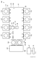
図1は、一実施形態に係る基板処理システムを示す概略平面図である。
Embodiments will be described below with reference to the accompanying drawings.
FIG. 1 is a schematic plan view showing a substrate processing system according to one embodiment.
本実施形態の基板処理システム100は、複数の基板に対して連続的に処理を実施するものである。基板の処理は特に限定されず、例えば成膜処理、エッチング処理、アッシング処理、クリーニング処理のような種々の処理を挙げることができる。基板は、特に限定されるものではないが、以下の説明では、基板として半導体ウエハ(以下単にウエハともいう)を用いた場合を例にとって説明する。
The
図1に示すように、基板処理システム100は、クラスタ構造(マルチチャンバタイプ)のシステムであり、複数の処理装置110、真空搬送室120、ロードロック室130、大気搬送室140、基板搬送装置150、および制御部160を備える。
As shown in FIG. 1, the
真空搬送室120は平面形状が矩形状をなし、内部が真空雰囲気に減圧され、長辺側の相対向する壁部に複数の処理室110がゲートバルブGを介して接続されている。また、真空搬送室120の短辺側の一方の壁部に2つのロードロック室130がゲートバルブG1を介して接続されている。2つのロードロック室130の真空搬送室120と反対側にはゲートバルブG2を介して大気搬送室140が接続されている。なお、図1において、処理室110の配列方向がX方向であり、X方向と直交する方向がY方向である。
The
真空搬送室120内の基板搬送装置150は、処理室110、ロードロック室130に対して、基板であるウエハWの搬入出を行う。基板搬送装置150は、実際にウエハWを保持するウエハ保持部であるエンドエフェクタ50を有する搬送ユニット20およびウエハ検出センサ60を有している。基板搬送装置150の詳細については後述する。
A
処理室110と真空搬送室120との間は、ゲートバルブGを開放することにより連通して基板搬送装置150によるウエハWの搬送が可能となり、ゲートバルブGを閉じることにより遮断される。また、ロードロック室130と真空搬送室120との間は、ゲートバルブG1を開放することにより連通して基板搬送装置150によるウエハWの搬送が可能となり、ゲートバルブG1を閉じることにより遮断される。
The
処理室110は、ウエハWを載置する載置台111を有し、内部が真空雰囲気に減圧された状態で載置台111に載置されたウエハWに対して所望の処理(成膜処理、エッチング処理、アッシング処理、クリーニング処理等)を施す。
The
ロードロック室130は、ウエハWを載置する載置台131を有し、大気搬送室140と真空搬送室120との間でウエハWを搬送する際に、大気圧と真空との間で圧力制御するものである。
The
大気搬送室140は、大気雰囲気となっており、例えば清浄空気のダウンフローが形成される。また、大気搬送室140の壁面には、ロードポート(図示せず)が設けられている。ロードポートは、ウエハWが収容されたキャリア(図示せず)または空のキャリアが接続されるように構成されている。キャリアとしては、例えば、FOUP(Front Opening Unified Pod)等を用いることができる。
The
また、大気搬送室140の内部には、ウエハWを搬送する大気搬送装置(図示せず)が設けられている。大気搬送装置は、ロードポート(図示せず)に収容されたウエハWを取り出して、ロードロック室130の載置台131に載置し、または、ロードロック室130の載置台131に載置されたウエハWを取り出して、ロードポートに収容する。ロードロック室130と大気搬送室140との間は、ゲートバルブG2を開放することにより連通して大気搬送装置によるウエハWの搬送が可能となり、ゲートバルブを閉じることにより遮断される。
An atmospheric transfer device (not shown) for transferring the wafer W is provided inside the
制御部160は、コンピュータで構成されており、CPUを備えた主制御部と、入力装置、出力装置、表示装置、記憶装置(記憶媒体)を有している。主制御部は、基板処理システム100の各構成部の動作を制御する。例えば、各処理室110におけるウエハWの処理、ゲートバルブG,G1,G2の開閉等を制御する。主制御部による各構成部の制御は、記憶装置に内蔵された記憶媒体(ハードディスク、光デスク、半導体メモリ等)に記憶された制御プログラムである処理レシピに基づいてなされる。
The
また、本実施形態では制御部160は、基板搬送装置150の一部である搬送制御部70を制御する。搬送制御部70については、後述する基板搬送装置150の説明において併せて説明する。
Further, in this embodiment, the
次に、基板処理システム100の動作の一例について説明する。ここでは、基板処理システム100の動作の一例として、ロードポートに取り付けられたキャリアに収容されたウエハWを処理室110で処理を施し、ロードポートに取り付けられた空のキャリアに収容する動作を説明する。なお、以下の動作は、制御部160の処理レシピに基づいて実行される。
Next, an example of the operation of the
まず、大気搬送室140内の大気搬送装置(図示せず)によりロードポートに接続されたキャリアからウエハWを取り出し、ゲートバルブG2を開けて大気雰囲気のロードロック室130に搬入する。そして、ゲートバルブG2を閉じた後、ウエハWが搬入されたロードロック室130を真空搬送室120に対応する真空状態とする。次いで、対応するゲートバルブG1を開けて、ロードロック室130の中のウエハWを、搬送ユニット20のエンドエフェクタ50により取り出し、ゲートバルブG1を閉じる。次いで、いずれかの処理室110に対応するゲートバルブGを開けた後、エンドエフェクタ50によりその処理室110にウエハWを搬入し載置台111に載置する。そして、その処理室110からエンドエフェクタ50を退避させ、ゲートバルブGを閉じた後、その処理室110で成膜処理等の処理が行われる。
First, an atmospheric transfer device (not shown) in the
処理室110での処理が終了した後、対応するゲートバルブGを開け、搬送ユニット20のエンドエフェクタ50が、その処理室110からウエハWを取り出す。そして、ゲートバルブGを閉じた後、ゲートバルブG1を開け、エンドエフェクタ50に保持されたウエハWを、ロードロック室130に搬送する。その後、ゲートバルブG1を閉じ、ウエハWが搬入されたロードロック室130を大気雰囲気とした後、ゲートバルブG2を開け、大気搬送装置(図示せず)によりロードロック室130からウエハWを取り出し、ロードポートのキャリア(いずれも図示せず)に収納する。
After the processing in the
以上の処理を複数のウエハWに対して同時並行的に行い、キャリア内の全てのウエハWについて処理を実施する。 The above processes are performed on a plurality of wafers W in parallel, and all the wafers W in the carrier are processed.
なお、上記説明では、基板搬送装置150により、いずれかの処理室110にウエハWを搬送し、その処理室110でウエハWの搬送を行っている間に、別のウエハWを他の処理室110にウエハWを搬送するパラレル搬送の場合を説明したが、これに限るものではない。例えば、1枚のウエハWを複数の処理室110に順次搬送するシリアル搬送であってもよい。
In the above description, the wafer W is transferred to one of the
[基板搬送装置の一例]
次に、基板搬送装置の一例について、上述の図1の他、図2~5に基づいて詳細に説明する。図2は基板搬送装置の搬送ユニットおよび平面モータを説明するための断面図、図3は平面モータの駆動原理を説明するための斜視図、図4はウエハ検出センサを説明するための側面図、図5は基板搬送装置の制御系を説明するためのブロック図である。
[Example of substrate transfer device]
Next, an example of the substrate transfer apparatus will be described in detail based on FIGS. 2 to 5 in addition to FIG. 1 described above. 2 is a cross-sectional view for explaining the transfer unit and planar motor of the substrate transfer apparatus, FIG. 3 is a perspective view for explaining the driving principle of the planar motor, FIG. 4 is a side view for explaining the wafer detection sensor, FIG. 5 is a block diagram for explaining the control system of the substrate transfer device.
基板搬送装置150は、図1に示すように、平面モータ(リニアユニット)10と、搬送ユニット20と、ウエハ検出センサ60と、搬送制御部70とを有する。
The
平面モータ(リニアユニット)10は、搬送ユニット20をリニア駆動する。平面モータ(リニアユニット)10は、真空搬送室120の底壁121で構成される本体部11と、本体部11の内部に全体に亘って配置された複数の電磁コイル12と、複数の電磁コイル12に個別的に給電して搬送ユニット20をリニア駆動するリニア駆動部13とを有している。リニア駆動部13は搬送制御部70の平面モータ制御部72により制御される。電磁コイル12に電流が供給されることにより、磁場が生成される。
A planar motor (linear unit) 10 linearly drives the
搬送ユニット20は、ウエハWを保持するウエハ保持部であるエンドエフェクタ50と、ベース30とを有する。なお、図では搬送ユニット20を1つ描いているが、搬送ユニット20は2つ以上でもよい。
The
図3に示すように、ベース30は、その中に複数の永久磁石35が配列されて構成されており、平面モータ(リニアユニット)10により駆動される。そして、ベース30の駆動にともなってエンドエフェクタ50が移動される。平面モータ(リニアユニット)10の電磁コイル12に供給する電流の向きを、それにより生成される磁場が永久磁石35と反発するような向きとすることにより、ベース30が本体部11表面から磁気浮上するように構成されている。ベース30は、電磁コイル12への電流を停止することにより、浮上が停止され、真空搬送室120の床面、すなわち平面モータ10の本体部11表面に載置された状態となる。また、平面モータ制御部72によりリニア駆動部13から電磁コイル12に供給する電流を個別的に制御することによって、ベース30を磁気浮上させた状態で、ベース30を平面モータ10の本体部11表面に沿って移動させ、その位置を制御することができる。また、電流の制御により浮上量も制御することができる。
As shown in FIG. 3, the
ウエハ検出センサ60は、真空搬送室120における各処理室110のウエハ搬入出口に対応する部分に設けられた2つのセンサ素子部61を有している。図4に示すように、センサ素子部61は、例えば、鉛直方向に配置された発光素子61aと受光素子61bとを有し、光センサを構成しており、ウエハWが発光素子61aおよび受光素子61bの間を通過した際にウエハWが検出される。また、図5に示すように、ウエハ検出センサ60は、センサ素子部61からの信号を受け取って計測する計測部62を有する。
The
搬送制御部70は、演算部71と上述した平面モータ制御部72とを有する。演算部71は、ウエハ検出センサ60の計測部62からの信号を取得し、エンドエフェクタ50上の実際のウエハWの位置を演算し、その演算結果によりウエハ位置の論理位置からの補正値を算出する。平面モータ制御部72は、その補正値に基づいて処理室110の載置台111におけるウエハWの搬送位置を修正し、その修正された搬送位置にウエハWが搬送されるようにリニア駆動部13を制御する。
The
このように構成される基板搬送装置150においては、平面モータ制御部72により平面モータ(リニアユニット)10のリニア駆動部13から電磁コイル12に供給する電流を制御して永久磁石35と反発する磁場を生成することにより、ベース30を磁気浮上させる。このときの浮上量は電流の制御により制御することができる。
In the
磁気浮上した状態で、リニア駆動部13から電磁コイル12に供給する電流を個別的に制御することにより、ベース30を平面モータ10の本体部11表面(真空搬送室120の床面)に沿って移動させ、その位置を制御することができる。これにより搬送ユニット20を移動および旋回させることができる。
In the magnetically levitated state, the
搬送ユニット20によりウエハWを処理室110に搬入する際には、エンドエフェクタ50の上にウエハWを載せた状態で、エンドエフェクタ50が処理室110に対応する位置になるようにベース30を移動させる。そして、ゲートバルブGを開けた後、さらにベース30を移動させてエンドエフェクタ50を処理室110内に挿入し、処理室110内の載置台111へウエハWを受け渡す。
When the
このとき、搬送制御部70は、保有している位置データに基づいてベース30の位置を制御し、ウエハWを処理室110内の載置台111上の目的位置へ搬送する。しかしながら、エンドエフェクタ50上でウエハWが予め設定された位置からずれて載置されることがある。
At this time, the
具体的には、図6に示すように、搬送制御部70にはエンドエフェクタ50に載置されているウエハWの中心の位置が論理中心O1と設定されており、搬送制御部70は、それに基づいてリニア駆動中心であるベース30の中心Mの位置制御を行う。しかし、実際にエンドエフェクタ50に載置されたウエハWの物理中心O2の位置が論理中心O1の位置からずれる場合がある。図6の例では、エンドエフェクタ50に載置されたウエハWの物理中心O2が論理中心O1からX方向にx、Y方向にyずれている状態を示している。
Specifically, as shown in FIG. 6, the
平面モータ10を用いたリニア駆動では従来用いていた搬送ロボットのような中心軸をもたないため、中心軸を基準点とした搬送補正を行えない。このため、ウエハWがエンドエフェクタ50上でずれた位置に載置されている場合、搬送制御部70によりウエハWの搬送位置を制御しても、ウエハWは載置台111上の搬送目的位置からずれた位置に載置される。
Since the linear drive using the
平面モータを用いた基板搬送は、上述したように、搬送ロボットを用いる技術における真空シールからのガスの侵入の問題や、搬送ロボットの移動が限定されるという問題を解決するものである。しかし、近時、デバイスの微細化の要求が厳しくなり、均一性や特性の改善のため、基板(ウエハ)の処理室の載置台への載置精度の要求は厳しくなっている。また、基板(ウエハ)の処理として高温処理や低温処理が存在し、そのような場合は熱膨張差により、上述のようなエンドエフェクタ上の基板の位置ずれが大きくなる傾向にある。そのため、エンドエフェクタ上の基板の位置ずれに起因した搬送目的位置に対する位置ずれが問題となる。 As described above, substrate transfer using a planar motor solves the problem of gas intrusion from a vacuum seal and the problem that the movement of the transfer robot is limited in the technique using the transfer robot. In recent years, however, the demand for miniaturization of devices has become stricter, and in order to improve uniformity and characteristics, the demand for mounting precision of substrates (wafers) on a mounting table in a processing chamber has become more stringent. Further, substrate (wafer) processing includes high-temperature processing and low-temperature processing, and in such cases, there is a tendency for the positional deviation of the substrate on the end effector as described above to increase due to the difference in thermal expansion. Therefore, positional deviation from the transport target position due to the positional deviation of the substrate on the end effector becomes a problem.
このため、本実施形態では、真空搬送室120における各処理室110のウエハ搬入出口に対応する部分にウエハ検出センサ60のセンサ素子部61を設け、エンドエフェクタ50上のウエハWを処理室110の載置台111に搬送する過程でセンサ素子部61によりウエハWの位置を検出する。そして、その検出データに基づいて、搬送制御部70の演算部71でエンドエフェクタ50上の実際のウエハWの位置を演算し、その演算結果によりウエハ位置の論理位置からの補正値を算出する。平面モータ制御部72は、その補正値に基づいて処理室110の載置台111におけるウエハWの搬送位置を修正する。そして、リニア駆動部13は修正された搬送位置にウエハWが搬送されるように搬送制御される。
For this reason, in the present embodiment, the
その際の搬送制御部70によるシーケンス例を図7に示す。
まず、リニア駆動部13に搬送目的位置であるウエハWの中心座標(X,Y)の指令を与える(ステップST1)。搬送目的位置は、処理室110の載置台111上の位置である。
FIG. 7 shows an example of the sequence by the
First, a command for the central coordinates (X, Y) of the wafer W, which is the transfer target position, is given to the linear drive unit 13 (step ST1). The transfer target position is a position on the mounting table 111 in the
次に、指令に基づいてリニア駆動部13を動作させる(ステップST2)。これにより、搬送ユニット20のベース30が移動され、これにともなってエンドエフェクタ50上のウエハWが搬送される。具体的には、ウエハWがエンドエフェクタ50に保持された状態で目的の処理室110に対応する位置までX方向に沿って搬送され、さらに目的の処理室110に向けてY方向へ搬送される。
Next, the
次に、ウエハ検出センサ60によりウエハWを検出する(ステップST3)。具体的には、2つのセンサ素子部61により通過するウエハWを検出し、その検出信号を計測部62で計測する。
Next, the
次に、ウエハ検出センサ60の検出データに基づいてエンドエフェクタ50上のウエハWの物理中心位置O2を演算し、論理中心O1からの補正値(x、y)を算出する(ステップST4)。
Next, the physical center position O2 of the wafer W on the
次に、補正値(x、y)に基づいてウエハWの搬送位置のウエハWの中心座標を(X+x,Y+y)に修正する(ステップST5)。リニア駆動部13はこの修正された搬送位置に基づいて搬送制御される。
Next, based on the correction values (x, y), the center coordinates of the transfer position of the wafer W are corrected to (X+x, Y+y) (step ST5). The
これにより、処理室110内の載置台111上の予め設定された搬送位置へ高い位置精度でウエハWを搬送することができる。
Thereby, the wafer W can be transferred to a preset transfer position on the mounting table 111 in the
ウエハ検出センサ60(センサ素子部61)は、処理室110ごとに配置されており、各処理室110にウエハWを搬送する度に同様の位置補正を行う。
The wafer detection sensor 60 (sensor element unit 61 ) is arranged for each
このような位置補正は、ウエハWの搬送形態がパラレル搬送であってもシリアル搬送であっても同様に行うことができる。 Such positional correction can be performed in the same way regardless of whether the transport mode of the wafer W is parallel transport or serial transport.
[基板搬送装置の他の例]
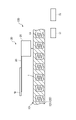
次に、基板搬送装置の他の例について説明する。本例では、搬送ユニットの構成が上記例とは異なっている。図8は本例の基板搬送装置の搬送ユニットを示す平面図であり、図9は本例の基板搬送装置の搬送ユニットを示す側面図である。なお、図8の(a)、(b)は搬送ユニットのそれぞれ異なる姿勢を示している。
[Another example of substrate transfer device]
Next, another example of the substrate transfer device will be described. In this example, the configuration of the transport unit is different from the above example. FIG. 8 is a plan view showing a transfer unit of the substrate transfer apparatus of this example, and FIG. 9 is a side view of the transfer unit of the substrate transfer apparatus of this example. Note that FIGS. 8A and 8B show different postures of the transport unit.
本例の搬送ユニット20´は、2つのベース31および32と、リンク機構(リンク41,42)と、エンドエフェクタ50とを有する。
The
ベース31,32は、上述の例のベース30と同様、その中に複数の永久磁石35(図3参照)が配列されて構成されており、リンク機構(リンク41,42)を介してエンドエフェクタ50を移動させる。平面モータ(リニアユニット)10の電磁コイル12に供給する電流の向きを、それにより生成される磁場が永久磁石35と反発するような向きとすることにより、ベース31,32が本体部11表面から磁気浮上する。
The
リンク機構を構成するリンク41,42は、2つのベース31,32と、エンドエフェクタ50とを接続する。具体的には、リンク41の一端側は、垂直方向の回転軸43を介して回転自在にベース31と接続されている。リンク41の他端側は、垂直方向の回転軸45を介して回転自在にエンドエフェクタ50と接続されている。リンク42の一端側は、垂直方向の回転軸44を介して回転自在にベース32と接続されている。リンク42の他端側は、垂直方向の回転軸46を介して回転自在にエンドエフェクタ50と接続されている。
また、リンク機構は、リンク角度が連動して動くように構成されていてもよい。例えば、リンク機構は、エンドエフェクタ50の延伸方向(回転軸45,46を結ぶ線に対して直交する方向)とリンク41のなす角と、エンドエフェクタ50の延伸方向とリンク42のなす角とが、同角となるように連動させる角度連動機構(図示せず)を備えていてもよい。角度連動機構(図示せず)は、例えば、ギアやベルト等によって構成される。これにより、リンク機構は、回転軸43,44の間隔(すなわちベース31,32の間隔)を変化させることにより、エンドエフェクタ50の向きを保ったまま伸縮することができる。
Further, the link mechanism may be configured so that the link angles move in conjunction with each other. For example, in the link mechanism, the angle formed by the extension direction of the end effector 50 (the direction perpendicular to the line connecting the rotation axes 45 and 46) and the
本例では、エンドエフェクタ50は、リンク機構(リンク41,42)に接続されている。そして、2つのベース31,32とエンドエフェクタ50とがリンク機構(リンク41,42)を介して接続されていることにより、エンドエフェクタ50を図8(a)の後退位置および図8(b)の前進位置に位置とすることができる。
In this example, the
すなわち、図8(a)の後退位置ではベース31,32の間隔がD1となり、エンドエフェクタ50の伸長距離H1が一意に決まる。また、図8(b)の前進位置ではベース31,32の間隔がD2となり、エンドエフェクタ50の伸長距離H2が一意に決まる。
That is, at the retracted position in FIG. 8A, the distance between the
なお、ベース31,32の間隔は、ベース31の基準位置とベース32の基準位置との距離であり、本例では、回転軸43と回転軸44との距離である。また、伸長距離は、ベース31の回転軸43とベース32の回転軸44とを結ぶ直線と、エンドエフェクタ50に載置されたウエハWの中心との距離である。また、47,48は、リンク41,42の回転角度を制限するストッパであり、必要に応じて設けられる。
The distance between the
このように構成される搬送ユニット20´では、平面モータ制御部72により平面モータ(リニアユニット)10のリニア駆動部13から電磁コイル12に供給する電流を制御して永久磁石35と反発する磁場を生成することにより、ベース31,32が磁気浮上した状態となる。磁気浮上した状態で、電磁コイル12に供給する電流を個別的に制御することにより、ベース31,32を平面モータ10の本体部11表面(真空搬送室120の床面)に沿って移動させ、その位置を制御することができる。これにより搬送ユニット20´を移動および旋回させることができる。
In the conveying unit 20' thus configured, the planar
また、ベース31,32の間隔が所望の間隔となるように、電磁コイル12に供給する電流を制御することにより、エンドエフェクタ50の延伸距離を変化させることができる。例えば、処理室110やロードロック室130にアクセスする際は、図8(b)に示すように、ベース31,32の間隔を狭くしてエンドエフェクタ50の延伸距離を長くする。これにより、ベース31,32を平面モータ10の本体部11表面(真空搬送室120の床面)上に存在させたまま、エンドエフェクタ50を処理室110内やロードロック室130内に挿入することができる。また、例えば、真空搬送室120内で搬送ユニット20´を移動および旋回させる際は、図8(a)に示すように、ベース31,32の間隔を広くしてエンドエフェクタ50の延伸距離を短くする。これによりウエハWを保持するエンドエフェクタ50をベース31,32に近づけることができ、リンク機構(リンク41,42)の垂れ、振動を小さくして搬送中のウエハWのずれを低減することができる。
Also, by controlling the current supplied to the
本例においても、上記例と同様、真空搬送室120における各処理室110のウエハ搬入出口に対応する部分にウエハ検出センサ60のセンサ素子部61を設け、エンドエフェクタ50上のウエハWを処理室110の載置台111に搬送する過程でセンサ素子部61によりウエハWの位置を検出する。そして、その検出データに基づいて、搬送制御部70の演算部71で実際のエンドエフェクタ上のウエハWの位置を演算し、その演算結果によりウエハ位置の論理位置からの補正値を算出する。平面モータ制御部72は、その補正値に基づいて処理室110の載置台111におけるウエハWの搬送位置を修正し、その修正された搬送位置にウエハWが搬送されるようにリニア駆動部13を制御する。
In this example, similarly to the above example, the
これにより、処理室110内の載置台111上の予め設定された搬送位置へ高い位置精度でウエハWを搬送することができる。
Thereby, the wafer W can be transferred to a preset transfer position on the mounting table 111 in the
<他の適用>
以上、実施形態について説明したが、今回開示された実施形態は、全ての点で例示であって制限的なものではないと考えられるべきである。上記の実施形態は、添付の特許請求の範囲およびその主旨を逸脱することなく、様々な形態で省略、置換、変更されてもよい。
<Other applications>
Although the embodiments have been described above, the embodiments disclosed this time should be considered as examples and not restrictive in all respects. The above-described embodiments may be omitted, substituted, or modified in various ways without departing from the scope and spirit of the appended claims.
例えば、上記実施形態では、基板処理システムの搬送ユニットとして、ベースが1つの例および2つの例を示したが、3つ以上であってもよい。また、ベースとエンドエフェクタとの間にリンク機構を用いる場合に、リンク機構として多関節のものを用いてもよく、また、水平方向に変位するリンク機構と高さ方向に変化するリンク機構を組み合わせてもよい。 For example, in the above-described embodiments, examples of one and two bases were shown as the transport unit of the substrate processing system, but the number of bases may be three or more. Further, when a link mechanism is used between the base and the end effector, a multi-joint link mechanism may be used as the link mechanism. may
また、上記実施形態ではウエハの搬送目的位置を処理室の載置台上としたが、これに限るものではない。 Further, in the above embodiment, the target transfer position of the wafer is on the mounting table of the processing chamber, but the present invention is not limited to this.
さらに、上記実施形態では、ウエハ検出センサとしてセンサ素子部が発光素子と受光素子を有する光センサを用いた例を示したが、これに限るものではない。 Furthermore, in the above embodiment, an example of using an optical sensor having a light emitting element and a light receiving element in the sensor element portion as the wafer detection sensor is shown, but the present invention is not limited to this.
さらにまた、基板として半導体ウエハ(ウエハ)を用いた場合について示したが、半導体ウエハに限らず、FPD(フラットパネルディスプレイ)基板や、石英基板、セラミックス基板等の他の基板であってもよい。 Furthermore, although the case of using a semiconductor wafer (wafer) as the substrate has been shown, the substrate is not limited to the semiconductor wafer, and may be another substrate such as an FPD (flat panel display) substrate, a quartz substrate, or a ceramics substrate.
10;平面モータ
11;本体部
12;電磁コイル
13;リニア駆動部
20,20´;搬送ユニット
30,31,32;ベース
35;永久磁石
41,42;リンク
50;エンドエフェクタ(基板保持部)
60;ウエハ検出センサ
61;センサ素子部
62;計測部
70;搬送制御部
71;演算部
72;平面モータ制御部
100;基板処理システム
110;処理室
120;真空搬送室
130;ロードロック室
140;大気搬送室
150;基板搬送装置
160;制御部
W;半導体ウエハ(基板)
10;
60;
Claims (14)
基板を保持する基板保持部、および、内部に磁石を有し、前記基板保持部を移動させるベースを有する搬送ユニットと、
本体部、前記本体部内に配列された複数の電磁コイル、および、前記電磁コイルに給電し、前記ベースを磁気浮上させるとともにリニア駆動するリニア駆動部を有する平面モータと、
前記基板保持部に保持された前記基板が通過した際に前記基板を検出する基板検出センサと、
前記基板検出センサの検出データに基づいて前記基板保持部に保持された前記基板の実際の位置を演算し、設定された論理位置に対する補正値を算出し、その補正値に基づいて前記基板の搬送位置を修正する搬送制御部と、
を有する、基板搬送装置。 A substrate transport device for transporting a substrate,
a substrate holding part that holds a substrate, and a transfer unit that has a magnet inside and a base that moves the substrate holding part;
a planar motor having a main body, a plurality of electromagnetic coils arranged in the main body, and a linear drive unit that supplies power to the electromagnetic coils to magnetically levitate the base and linearly drive the base;
a substrate detection sensor that detects the substrate when the substrate held by the substrate holding portion passes;
calculating the actual position of the substrate held by the substrate holding unit based on the detection data of the substrate detection sensor, calculating a correction value for the set logical position, and transporting the substrate based on the correction value a transport control unit that corrects the position;
A substrate transport apparatus.
基板を保持する基板保持部、および、内部に磁石を有し、前記基板保持部を移動させるベースを有する搬送ユニットと、本体部、前記本体部内に配列された複数の電磁コイル、および、前記電磁コイルに給電し、前記ベースを磁気浮上させるとともにリニア駆動するリニア駆動部を有する平面モータと、を有する基板搬送装置を用い、
前記基板を前記基板保持部に保持させた状態で前記基板を搬送する過程で、基板検出センサにより前記基板を検出することと、
前記基板検出センサの検出データに基づいて前記基板保持部に保持された前記基板の実際の位置を演算し、設定された論理位置に対する補正値を算出することと、
その補正値に基づいて前記基板の搬送位置を修正することと、
を有する、基板搬送方法。 A substrate transport method for transporting a substrate,
a substrate holding portion that holds a substrate; a transfer unit that has a magnet inside and a base that moves the substrate holding portion; a body portion; a plurality of electromagnetic coils arranged in the body portion; a planar motor having a linear drive unit that supplies power to a coil to magnetically levitate the base and linearly drive the base,
detecting the substrate by a substrate detection sensor in the process of transporting the substrate while the substrate is held by the substrate holding part;
calculating an actual position of the substrate held by the substrate holding unit based on detection data of the substrate detection sensor, and calculating a correction value for the set logical position;
correcting the transfer position of the substrate based on the correction value;
A substrate transfer method.
前記処理室が接続された搬送室と、
前記搬送室の内部に設けられ、前記処理室内の搬送位置へ前記基板を搬送する基板搬送装置と、
を具備し、
前記基板搬送装置は、
基板を保持する基板保持部、および、内部に磁石を有し、前記基板保持部を移動させるベースを有する搬送ユニットと、
本体部、前記本体部内に配列された複数の電磁コイル、および、前記電磁コイルに給電し、前記ベースを磁気浮上させるとともにリニア駆動するリニア駆動部を有する平面モータと、
前記基板保持部に保持された前記基板が通過した際に前記基板を検出する基板検出センサと、
前記基板検出センサの検出データに基づいて前記基板保持部に保持された前記基板の実際の位置を演算し、設定された論理位置に対する補正値を算出し、その補正値に基づいて前記基板の搬送位置を修正する搬送制御部と、
を有する、基板処理システム。 a processing chamber for processing the substrate;
a transfer chamber to which the processing chamber is connected;
a substrate transfer device provided inside the transfer chamber for transferring the substrate to a transfer position in the processing chamber;
and
The substrate transfer device is
a substrate holding part that holds a substrate, and a transfer unit that has a magnet inside and a base that moves the substrate holding part;
a planar motor having a main body, a plurality of electromagnetic coils arranged in the main body, and a linear drive unit that supplies power to the electromagnetic coils to magnetically levitate the base and linearly drive the base;
a substrate detection sensor that detects the substrate when the substrate held by the substrate holding portion passes;
calculating the actual position of the substrate held by the substrate holding unit based on the detection data of the substrate detection sensor, calculating a correction value for the set logical position, and transporting the substrate based on the correction value a transport control unit that corrects the position;
A substrate processing system comprising:
Priority Applications (5)
| Application Number | Priority Date | Filing Date | Title |
|---|---|---|---|
| JP2021002579A JP2022107898A (en) | 2021-01-12 | 2021-01-12 | Substrate conveying device, substrate conveying method, and substrate processing system |
| KR1020210190678A KR102652598B1 (en) | 2021-01-12 | 2021-12-29 | Substrate transfer apparatus, substrate transfer method, and substrate processing system |
| TW110149399A TW202234562A (en) | 2021-01-12 | 2021-12-29 | Substrate transfer apparatus, substrate transfer method, and substrate processing system |
| CN202210002402.XA CN114765121A (en) | 2021-01-12 | 2022-01-04 | Substrate transfer apparatus, substrate transfer method, and substrate processing system |
| US17/573,387 US20220223447A1 (en) | 2021-01-12 | 2022-01-11 | Substrate transfer apparatus, substrate transfer method, and substrate processing system |
Applications Claiming Priority (1)
| Application Number | Priority Date | Filing Date | Title |
|---|---|---|---|
| JP2021002579A JP2022107898A (en) | 2021-01-12 | 2021-01-12 | Substrate conveying device, substrate conveying method, and substrate processing system |
Publications (2)
| Publication Number | Publication Date |
|---|---|
| JP2022107898A true JP2022107898A (en) | 2022-07-25 |
| JP2022107898A5 JP2022107898A5 (en) | 2023-09-07 |
Family
ID=82323252
Family Applications (1)
| Application Number | Title | Priority Date | Filing Date |
|---|---|---|---|
| JP2021002579A Pending JP2022107898A (en) | 2021-01-12 | 2021-01-12 | Substrate conveying device, substrate conveying method, and substrate processing system |
Country Status (5)
| Country | Link |
|---|---|
| US (1) | US20220223447A1 (en) |
| JP (1) | JP2022107898A (en) |
| KR (1) | KR102652598B1 (en) |
| CN (1) | CN114765121A (en) |
| TW (1) | TW202234562A (en) |
Families Citing this family (1)
| Publication number | Priority date | Publication date | Assignee | Title |
|---|---|---|---|---|
| JP2022107906A (en) * | 2021-01-12 | 2022-07-25 | 東京エレクトロン株式会社 | Substrate conveying device, substrate conveying method, and substrate processing system |
Family Cites Families (6)
| Publication number | Priority date | Publication date | Assignee | Title |
|---|---|---|---|---|
| JPH06120317A (en) * | 1992-03-20 | 1994-04-28 | Ulvac Japan Ltd | Wafer carriage mechanism for vacuumizer |
| JP2003264214A (en) | 2002-03-07 | 2003-09-19 | Hitachi High-Technologies Corp | Vacuum treatment device and vacuum treatment method |
| JP5600703B2 (en) * | 2012-03-30 | 2014-10-01 | 東京エレクトロン株式会社 | Conveying apparatus and conveying method |
| KR20150034143A (en) | 2012-07-04 | 2015-04-02 | 도쿄엘렉트론가부시키가이샤 | Substrate processing equipment |
| TWI732285B (en) * | 2015-01-23 | 2021-07-01 | 美商應用材料股份有限公司 | Semiconductor process equipment |
| KR102099115B1 (en) * | 2018-06-08 | 2020-04-10 | 세메스 주식회사 | Apparatus for transferring substrate, apparatus for treating substrate and method for compensating distortion of substrate |
-
2021
- 2021-01-12 JP JP2021002579A patent/JP2022107898A/en active Pending
- 2021-12-29 KR KR1020210190678A patent/KR102652598B1/en active IP Right Grant
- 2021-12-29 TW TW110149399A patent/TW202234562A/en unknown
-
2022
- 2022-01-04 CN CN202210002402.XA patent/CN114765121A/en active Pending
- 2022-01-11 US US17/573,387 patent/US20220223447A1/en active Pending
Also Published As
| Publication number | Publication date |
|---|---|
| TW202234562A (en) | 2022-09-01 |
| CN114765121A (en) | 2022-07-19 |
| US20220223447A1 (en) | 2022-07-14 |
| KR102652598B1 (en) | 2024-03-28 |
| KR20220102108A (en) | 2022-07-19 |
Similar Documents
| Publication | Publication Date | Title |
|---|---|---|
| US11664259B2 (en) | Process apparatus with on-the-fly substrate centering | |
| WO2021106796A1 (en) | Substrate conveyance apparatus and substrate processing system | |
| KR20180030171A (en) | On the fly automatic wafer centering method and apparatus | |
| JP6063716B2 (en) | Substrate processing apparatus and substrate transfer method | |
| JP4534886B2 (en) | Processing system | |
| WO2021106799A1 (en) | Substrate transport device and substrate processing system | |
| CN114758975A (en) | Method and apparatus for automatic wafer centering during transport | |
| US20220037181A1 (en) | Vacuum transfer device, substrate processing system, and substrate processing method | |
| KR102652598B1 (en) | Substrate transfer apparatus, substrate transfer method, and substrate processing system | |
| JP2022165301A (en) | Device for conveying substrate, and method for conveying substrate | |
| JP2022133867A (en) | Substrate transfer device and substrate processing system | |
| KR102652600B1 (en) | Substrate transport apparatus, substrate transport method, and substrate processing system | |
| US20230307278A1 (en) | Substrate processing system | |
| JP7156332B2 (en) | Conveying Device, Conveying Method and Conveying System | |
| JP7257914B2 (en) | Substrate processing system and substrate processing method | |
| JP7236934B2 (en) | SUBSTRATE PROCESSING SYSTEM AND CONTROL METHOD OF SUBSTRATE PROCESSING SYSTEM |
Legal Events
| Date | Code | Title | Description |
|---|---|---|---|
| A521 | Request for written amendment filed |
Free format text: JAPANESE INTERMEDIATE CODE: A523 Effective date: 20230830 |
|
| A621 | Written request for application examination |
Free format text: JAPANESE INTERMEDIATE CODE: A621 Effective date: 20230830 |
|
| A977 | Report on retrieval |
Free format text: JAPANESE INTERMEDIATE CODE: A971007 Effective date: 20240415 |