JP2022074445A - Analog-to-digital conversion circuit, photoelectric conversion apparatus, and photoelectric conversion system - Google Patents
Analog-to-digital conversion circuit, photoelectric conversion apparatus, and photoelectric conversion system Download PDFInfo
- Publication number
- JP2022074445A JP2022074445A JP2020184492A JP2020184492A JP2022074445A JP 2022074445 A JP2022074445 A JP 2022074445A JP 2020184492 A JP2020184492 A JP 2020184492A JP 2020184492 A JP2020184492 A JP 2020184492A JP 2022074445 A JP2022074445 A JP 2022074445A
- Authority
- JP
- Japan
- Prior art keywords
- analog
- period
- circuit
- digital conversion
- photoelectric conversion
- Prior art date
- Legal status (The legal status is an assumption and is not a legal conclusion. Google has not performed a legal analysis and makes no representation as to the accuracy of the status listed.)
- Pending
Links
- 238000006243 chemical reaction Methods 0.000 title claims abstract description 175
- 238000000034 method Methods 0.000 claims description 33
- 230000008569 process Effects 0.000 claims description 28
- 230000015654 memory Effects 0.000 claims description 24
- 239000000758 substrate Substances 0.000 claims description 14
- 239000004065 semiconductor Substances 0.000 claims description 13
- 230000008859 change Effects 0.000 description 17
- 238000003384 imaging method Methods 0.000 description 8
- 230000007704 transition Effects 0.000 description 8
- 102100040862 Dual specificity protein kinase CLK1 Human genes 0.000 description 7
- 238000001514 detection method Methods 0.000 description 5
- 238000010586 diagram Methods 0.000 description 4
- 230000003287 optical effect Effects 0.000 description 4
- 102100040844 Dual specificity protein kinase CLK2 Human genes 0.000 description 3
- 101000749294 Homo sapiens Dual specificity protein kinase CLK1 Proteins 0.000 description 3
- 101000749291 Homo sapiens Dual specificity protein kinase CLK2 Proteins 0.000 description 3
- 230000000694 effects Effects 0.000 description 3
- 230000006870 function Effects 0.000 description 3
- 230000001360 synchronised effect Effects 0.000 description 2
- 230000003321 amplification Effects 0.000 description 1
- 230000004888 barrier function Effects 0.000 description 1
- 230000006835 compression Effects 0.000 description 1
- 238000007906 compression Methods 0.000 description 1
- 238000012937 correction Methods 0.000 description 1
- 230000003111 delayed effect Effects 0.000 description 1
- 230000006866 deterioration Effects 0.000 description 1
- 238000005259 measurement Methods 0.000 description 1
- 238000003199 nucleic acid amplification method Methods 0.000 description 1
- 230000000644 propagated effect Effects 0.000 description 1
- 230000009467 reduction Effects 0.000 description 1
- 230000000630 rising effect Effects 0.000 description 1
- 238000005070 sampling Methods 0.000 description 1
Images


Classifications
-
- H—ELECTRICITY
- H03—ELECTRONIC CIRCUITRY
- H03M—CODING; DECODING; CODE CONVERSION IN GENERAL
- H03M1/00—Analogue/digital conversion; Digital/analogue conversion
- H03M1/12—Analogue/digital converters
- H03M1/50—Analogue/digital converters with intermediate conversion to time interval
- H03M1/56—Input signal compared with linear ramp
-
- H—ELECTRICITY
- H04—ELECTRIC COMMUNICATION TECHNIQUE
- H04N—PICTORIAL COMMUNICATION, e.g. TELEVISION
- H04N25/00—Circuitry of solid-state image sensors [SSIS]; Control thereof
- H04N25/70—SSIS architectures; Circuits associated therewith
- H04N25/76—Addressed sensors, e.g. MOS or CMOS sensors
- H04N25/77—Pixel circuitry, e.g. memories, A/D converters, pixel amplifiers, shared circuits or shared components
- H04N25/772—Pixel circuitry, e.g. memories, A/D converters, pixel amplifiers, shared circuits or shared components comprising A/D, V/T, V/F, I/T or I/F converters
-
- H—ELECTRICITY
- H03—ELECTRONIC CIRCUITRY
- H03M—CODING; DECODING; CODE CONVERSION IN GENERAL
- H03M1/00—Analogue/digital conversion; Digital/analogue conversion
- H03M1/004—Reconfigurable analogue/digital or digital/analogue converters
- H03M1/007—Reconfigurable analogue/digital or digital/analogue converters among different resolutions
-
- H—ELECTRICITY
- H03—ELECTRONIC CIRCUITRY
- H03M—CODING; DECODING; CODE CONVERSION IN GENERAL
- H03M1/00—Analogue/digital conversion; Digital/analogue conversion
- H03M1/12—Analogue/digital converters
- H03M1/1205—Multiplexed conversion systems
- H03M1/123—Simultaneous, i.e. using one converter per channel but with common control or reference circuits for multiple converters
-
- H—ELECTRICITY
- H04—ELECTRIC COMMUNICATION TECHNIQUE
- H04N—PICTORIAL COMMUNICATION, e.g. TELEVISION
- H04N25/00—Circuitry of solid-state image sensors [SSIS]; Control thereof
- H04N25/70—SSIS architectures; Circuits associated therewith
- H04N25/71—Charge-coupled device [CCD] sensors; Charge-transfer registers specially adapted for CCD sensors
- H04N25/745—Circuitry for generating timing or clock signals
-
- H—ELECTRICITY
- H04—ELECTRIC COMMUNICATION TECHNIQUE
- H04N—PICTORIAL COMMUNICATION, e.g. TELEVISION
- H04N25/00—Circuitry of solid-state image sensors [SSIS]; Control thereof
- H04N25/70—SSIS architectures; Circuits associated therewith
- H04N25/71—Charge-coupled device [CCD] sensors; Charge-transfer registers specially adapted for CCD sensors
- H04N25/75—Circuitry for providing, modifying or processing image signals from the pixel array
Abstract
Description
本発明は、アナログデジタル変換回路、この回路を備えた光電変換装置、この光電変換装置を備えた撮像システムに関する。 The present invention relates to an analog-to-digital conversion circuit, a photoelectric conversion device provided with this circuit, and an imaging system provided with the photoelectric conversion device.
光電変換装置において、アレイ状に配置された画素の列ごとにアナログデジタル変換(以下、AD変換)部を配置して、各画素で生じた電荷に基づく画素信号をデジタルデータに変換する技術がある。特許文献1のAD変換部は、時間の経過とともに電位が変化する参照信号の電位と、画素信号の電位との大小関係を比較し、AD変換開始から参照信号と画素信号の電位の大小関係が反転するまでの時間を計測することでAD変換を実現している。特許文献1では、時間を計測する手段として、列ごとに列メモリを設け、複数列の列メモリに共通に接続される共通カウンタを用いて、参照信号と画素信号の電位の大小関係の反転に応じたカウント値を各列で列メモリに記憶する。
In a photoelectric conversion device, there is a technique of arranging an analog-digital conversion (hereinafter referred to as AD conversion) unit for each row of pixels arranged in an array to convert a pixel signal based on the electric charge generated in each pixel into digital data. .. The AD conversion unit of
特許文献1に記載の光電変換装置では、カウンタ回路の動作が入射光の輝度によらず一定であるため、カウンタ回路の消費電力が大きくなるという課題があった。
In the photoelectric conversion device described in
本発明は上記課題を鑑みてなされたものであり、カウンタ回路の消費電力低減を実現することを目的とする。 The present invention has been made in view of the above problems, and an object of the present invention is to reduce the power consumption of a counter circuit.
本発明の一つの側面は、アナログ信号とランプ信号とを比較処理する比較回路と、前記比較回路での前記比較処理に並行してカウント処理を行うカウンタ部と、を有し、前記比較処理に応じたカウント値であるデジタルデータを取得することによって前記アナログ信号のアナログデジタル変換を行うアナログデジタル変換回路であって、1つの前記アナログ信号のアナログデジタル変換の開始から終了までの期間に第1の期間および前記第1の期間の後の第2の期間が含まれ、前記第1の期間では前記カウント処理が高速に実行され、前記第2の期間では前記カウント処理が低速に実行されることを特徴とする。 One aspect of the present invention includes a comparison circuit that performs comparison processing between an analog signal and a lamp signal, and a counter unit that performs count processing in parallel with the comparison processing in the comparison circuit. It is an analog-to-digital conversion circuit that performs analog-to-digital conversion of the analog signal by acquiring digital data having a corresponding count value, and is the first in the period from the start to the end of the analog-to-digital conversion of one analog signal. A period and a second period after the first period are included, the counting process being executed at a high speed in the first period, and the counting process being executed at a low speed in the second period. It is a feature.
本発明の別の側面は、アナログ信号とランプ信号とを比較処理する比較回路と、前記比較回路での前記比較処理に並行してカウント処理を行うカウンタ部と、を有し、前記比較処理に応じたカウント値であるデジタルデータを取得することによって前記アナログ信号のアナログデジタル変換を行うアナログデジタル変換回路であって、1つの前記アナログ信号のアナログデジタル変換の開始から終了までの期間に第1の期間および前記第1の期間の後の第2の期間が含まれ、前記第1の期間では、第一の分解能で前記アナログデジタル変換回路が前記アナログデジタル変換を行い、前記第2の期間では、前記第一の分解能よりも低い第二の分解能で前記アナログデジタル変換回路が前記アナログデジタル変換を行うことを特徴とする。 Another aspect of the present invention includes a comparison circuit that performs comparison processing between an analog signal and a lamp signal, and a counter unit that performs count processing in parallel with the comparison processing in the comparison circuit. It is an analog-to-digital conversion circuit that performs analog-to-digital conversion of the analog signal by acquiring digital data having a corresponding count value, and is the first in the period from the start to the end of the analog-to-digital conversion of one of the analog signals. A period and a second period after the first period are included, in which the analog-to-digital conversion circuit performs the analog-to-digital conversion at the first resolution and in the second period. It is characterized in that the analog-to-digital conversion circuit performs the analog-to-digital conversion with a second resolution lower than the first resolution.
本発明の更に別の側面は、アナログ信号と、ランプ信号とを比較処理する比較回路と、複数ビットを有するカウント値を出力するカウンタ部を含み、前記カウンタ部は前記比較回路での前記比較処理に並行してカウント処理を行うことによって前記カウント値を出力し、前記比較処理に応じたカウント値であるデジタルデータを取得してアナログデジタル変換を行うアナログデジタル変換回路であって、1つの前記アナログ信号のアナログデジタル変換の開始から終了までの期間に第1の期間および前記第1の期間の後の第2の期間が含まれ、前記第1の期間において信号が変化する、前記複数ビットの最下位ビット側から少なくとも1ビットが、前記第2の期間においては所定の電位に固定されることを特徴とする。 Yet another aspect of the present invention includes a comparison circuit that compares and processes an analog signal and a lamp signal, and a counter unit that outputs a count value having a plurality of bits. The counter unit is the comparison process in the comparison circuit. An analog-to-digital conversion circuit that outputs the count value by performing count processing in parallel with the above, acquires digital data that is the count value according to the comparison process, and performs analog-to-digital conversion. The period from the start to the end of the analog-to-digital conversion of the signal includes a first period and a second period after the first period, and the signal changes in the first period. It is characterized in that at least one bit from the lower bit side is fixed to a predetermined potential in the second period.
本発明の更に別の側面は、アナログ信号と、ランプ信号とを比較処理する比較回路と、カウンタ部を有し、前記カウンタ部は前記比較回路での前記比較処理に並行してカウント処理を行い、前記比較処理に応じたカウント値であるデジタルデータを取得してアナログデジタル変換を行うアナログデジタル変換回路であって、1つの前記アナログ信号のアナログデジタル変換の開始から終了までの期間に第1の期間および前記第1の期間の後の第2の期間が含まれ、前記第2の期間における前記カウンタ部の動作周波数が前記第1の期間における前記カウンタ部の動作周波数よりも小さいことを特徴とする。 Yet another aspect of the present invention includes a comparison circuit for comparing and processing an analog signal and a lamp signal, and a counter unit, and the counter unit performs counting processing in parallel with the comparison processing in the comparison circuit. An analog-to-digital conversion circuit that acquires digital data that is a count value according to the comparison process and performs analog-to-digital conversion, and is the first in a period from the start to the end of analog-to-digital conversion of one analog signal. A period and a second period after the first period are included, and the operating frequency of the counter unit in the second period is smaller than the operating frequency of the counter unit in the first period. do.
本発明によれば、入射する光の輝度に応じてAD変換の分解能を最適化することで、カウンタ回路の消費電力の低減が実現できる。 According to the present invention, it is possible to reduce the power consumption of the counter circuit by optimizing the resolution of AD conversion according to the brightness of the incident light.
以下、図面を参照しながら各実施形態を説明する。 Hereinafter, each embodiment will be described with reference to the drawings.
以下に述べる各実施形態では、本発明を適用可能な装置の一例として、光電変換装置の一例である撮像装置を中心に説明する。ただし、各実施形態は、光電変換装置に限られるものではなく、他の装置にも適用可能である。また、光電変換装置への適用についても撮像装置に限られるものではない。例えば、測距装置(焦点検出やTOF(Time Of Flight)を用いた距離測定等の装置)、測光装置(入射光量の測定等の装置)などに適用可能である。 In each embodiment described below, an image pickup device, which is an example of a photoelectric conversion device, will be mainly described as an example of a device to which the present invention can be applied. However, each embodiment is not limited to the photoelectric conversion device, and can be applied to other devices. Further, the application to the photoelectric conversion device is not limited to the image pickup device. For example, it can be applied to a distance measuring device (a device for measuring a distance using a focus detection or TOF (Time Of Flight)), a photometric device (a device for measuring an incident light amount, etc.), and the like.
[第1の実施形態]
本発明の第一の実施形態について図1から図8を用いて説明する。
[First Embodiment]
The first embodiment of the present invention will be described with reference to FIGS. 1 to 8.
(光電変換装置の全体構成)
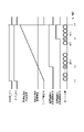
図1は本実施形態にかかる光電変換装置の構成を示した概略図である。本実施形態の光電変換装置は、画素部1と、読み出し回路2と、比較回路3と、列メモリ4と、水平走査回路5と、ランプ源6と、カウンタ回路7と、演算処理回路8と、ゲーティング部12と、バッファ部13とを含む。
(Overall configuration of photoelectric conversion device)
FIG. 1 is a schematic view showing the configuration of a photoelectric conversion device according to the present embodiment. The photoelectric conversion device of this embodiment includes a
画素部1には、複数行及び複数列に渡ってアレイ状に配された複数の画素が設けられている。画素部1の画素アレイの各行には、列方向(図1において縦方向)に延在して、読み出し回路2が配されている。読み出し回路2は、列方向に並ぶ画素のそれぞれに列ごとに接続され、これらの画素で生じる電荷をアナログ信号である画素信号として出力する共通の信号線をなしている。
The
画素部1を構成する画素の数は、特に限定されるものではない。例えば、一般的なデジタルカメラのように数千行×数千列の画素で画素部1を構成してもよく、1行又は1列に並べた複数の画素で画素部1を構成してもよい。
The number of pixels constituting the
カウンタ回路7より出力されるカウント値はゲーティング部12やバッファ部13を介して列メモリ4に入力される。ゲーティング部12とバッファ部13は、図に示したように複数列ごとに配置される。
The count value output from the
比較回路3は、画素アレイの列ごとに読み出し回路2に接続されている。比較回路3には読み出し回路2の出力信号と、ランプ源6で生成されるランプ信号とが入力され、入力される信号同士の電位の大きさを比較する。読み出し回路2より出力される信号とランプ信号との電位の大小関係の反転によって時、比較回路3の出力電位も反転する。比較回路3の出力電位の反転によってカウンタ回路7から出力されるカウント値が列メモリ4にデジタルデータとして記憶される。この出力信号とランプ信号との比較処理を画素のリセット信号である出力信号と画素信号である出力信号とで1回ずつ行い、それぞれのデジタルデータを取得する。
The
列メモリ4に記憶されたデジタルデータは、水平走査回路5から出力される信号によって、列ごとに演算処理回路8に順次転送される。演算処理回路8では、リセット信号に対応するデジタルデータと画素信号に対応するデジタルデータを減算する演算処理を行うことで、デジタルCDS(デジタル相関二重サンプリング)を実現する。なお、図1において各回路に必要なパルスとそのタイミングを制御する回路は省略している。
The digital data stored in the
(光電変換装置のAD変換)
光電変換装置のAD変換動作について図2のタイミングチャートを用いて詳細に説明する。
(AD conversion of photoelectric conversion device)
The AD conversion operation of the photoelectric conversion device will be described in detail with reference to the timing chart of FIG.
図2は、輝度によらずAD変換の分解能が一定な場合のタイミングチャートである。以下の説明では、入射される光の輝度が高くなると、読み出し回路2の処理により画素信号のレベルは高くなるものとする。読み出し回路2は例えば反転増幅アンプを含む。
FIG. 2 is a timing chart when the resolution of AD conversion is constant regardless of the luminance. In the following description, it is assumed that the level of the pixel signal increases due to the processing of the
時刻T1でランプ源6の制御信号RAMP_ENおよびカウンタ回路7の制御信号CNT_ENがHighになる。RAMP_ENがHighになると、ランプ源6は、時間の経過とともに電位が上昇するランプ信号を出力する。また、CNT_ENがHighになるとカウンタ回路7がカウント動作を開始し、ランプ信号の変化に並行してカウント動作が行われる。
At time T1, the control signal RAMP_EN of the
ここで、ランプ信号は時間経過に応じて連続的に電位が上昇するような信号でもよいし、ノコギリ状に電位が変化する信号でも構わない。前者の場合、電位の立ち上がりで電位変化が鈍る場合も許容される。 Here, the lamp signal may be a signal in which the potential continuously rises with the passage of time, or may be a signal in which the potential changes like a saw. In the former case, it is permissible that the potential change becomes dull due to the rise of the potential.
入射光が低輝度の時の画素信号は、入射光が高輝度の時の画素信号よりもレベルが低いので、時間の経過とともに電位が上昇するランプ信号では画素信号の電位とランプ信号の電位の大小関係が反転するタイミングは高輝度の時よりも低輝度の時の方が早い。 Since the pixel signal when the incident light has low brightness has a lower level than the pixel signal when the incident light has high brightness, the potential of the pixel signal and the potential of the lamp signal in the lamp signal whose potential rises with the passage of time. The timing at which the magnitude relationship is reversed is earlier when the brightness is low than when the brightness is high.
低輝度の光が入射した時、画素信号とランプ信号の両電位の大小関係が反転する時刻をT2とする。同時刻で比較回路出力はLowからHighに遷移する。比較回路出力がLowからHighに遷移すると、列メモリ4はこのときのカウント値M(Mは整数)を記憶する。
When low-luminance light is incident, the time at which the magnitude relationship between the two potentials of the pixel signal and the lamp signal is inverted is defined as T2. At the same time, the comparison circuit output transitions from Low to High. When the comparison circuit output changes from Low to High, the
高輝度の光が入射した時の画素信号は低輝度の光が入射したときの画素信号よりもレベルが高いので、画素信号の電位とランプ信号の電位の大小関係が反転するタイミングは時刻T2よりも遅くなる。高輝度の光が入射した時の両電位の大小関係が反転する時刻をT3とすると、時刻T3で比較回路出力がLowからHighに遷移し、列メモリはその時のカウント値N(Nは整数、N>M)を記憶する。 Since the pixel signal when high-intensity light is incident has a higher level than the pixel signal when low-intensity light is incident, the timing at which the magnitude relationship between the potential of the pixel signal and the potential of the lamp signal is inverted is from time T2. Will also be late. Assuming that the time at which the magnitude relationship between the two potentials when high-luminance light is incident is inverted is T3, the comparison circuit output transitions from Low to High at time T3, and the column memory has a count value N at that time (N is an integer, Memorize N> M).
時刻T4になるとRAMP_ENおよびCNT_ENがLowになり、ランプ源出力も電位の上昇を停止して基準電位に戻る。ここで基準電位とはランプ信号が電位の上昇を開始する時点の電位を指すものとする。カウンタ回路7はカウント動作を終了する。以上の動作を行うことでAD変換を実現する。上記AD変換に用いる回路を以降アナログデジタル変換回路(AD変換回路)と称する。
At time T4, RAMP_EN and CNT_EN become Low, and the lamp source output also stops rising in potential and returns to the reference potential. Here, the reference potential refers to the potential at the time when the lamp signal starts to rise in potential. The
上記のAD変換手法では、入射光の輝度が高くなるにつれて、比較回路がLowからHighに遷移するタイミングが遅くなる。つまり、入射光の輝度が高くなるにつれて、列メモリが記憶するカウント値は大きくなる。 In the above AD conversion method, as the brightness of the incident light increases, the timing at which the comparison circuit transitions from Low to High becomes delayed. That is, as the brightness of the incident light increases, the count value stored in the column memory increases.
なお、図2に示したタイミングチャートは一例であり、本実施形態を限定するものではない。 The timing chart shown in FIG. 2 is an example, and does not limit the present embodiment.
(本実施形態の駆動)
図3、図4を用いて本実施形態の駆動について説明する。
(Drive of this embodiment)
The driving of this embodiment will be described with reference to FIGS. 3 and 4.
図3(A)および(B)はカウンタ回路7をKビット(Kは整数)のグレイコードカウンタとした場合の、各列メモリに入力される各ビットの動作を示したタイミングチャートである。図3(A)は、輝度によらず、AD変換の分解能を一定とした場合のタイミングチャートである。図3(B)は本実施形態を適用し、高輝度領域で下位ビットの動作を止めた場合のタイミングチャートである。図3(B)では、カウンタ回路7のKビット目がLowからHighに遷移する時刻Tjより前の第1の期間に比較回路3出力が反転する場合の輝度を低輝度とし、時刻Tjより後の第2の期間に比較回路出力が反転する場合の輝度を高輝度としている。
3A and 3B are timing charts showing the operation of each bit input to each column memory when the
図4は図3(B)に示したタイミングチャートの動作を実現するカウンタ回路7とゲーティング部12の一例である。
FIG. 4 is an example of a
ゲーティング部12は、カウンタ回路7の各ビット出力に接続されるAND回路40と、AND回路40のそれぞれに接続されるバッファ回路41と、インバータ回路42とで構成される。図示した通り、バッファ回路41の出力が、ゲーティング部12の出力となる。3ビット目からKビット目までのAND回路40のもう一方の入力端子には、Highレベルの信号が入力され、1、2ビット目のAND回路40の入力端子にはカウンタ回路7のKビット目の出力がインバータ回路42によって反転された信号が入力される。よって、1、2ビット目のAND回路40出力は、カウンタ回路7のKビット目がHighになるとLowに固定され、1、2ビット目のAND回路40に接続されたバッファ回路41の出力もLowに固定される。AND回路40にHigh信号が入力されているその他のビットは、輝度によらず、カウンタ回路7の出力をバッファ回路を介して出力する。ここで、High信号には例えばゲーティング部12内で使用する電源電圧を接続すればよい。
The
以上のようにゲーティング部12を構成することによって、図3(B)のタイミングチャートに示した動作が実現可能である。図4に示したゲーティング部12により、高輝度側で1、2ビット目がゲーティングされるので、次段以降のバッファ部も1、2ビット目は動作しない。よって、ゲーティング部12およびバッファ部13が輝度によらず全ビット動作する図3(A)に示したタイミングチャートの動作より、本実施形態の図3(B)に示したタイミングチャートの動作の方が消費電力を低減できる。言い換えれば、カウント処理を高速に実行する第1の期間に対し、第2の期間ではカウント処理を低速に実行することで消費電力を低減することが可能である。
By configuring the
ここで、下位ビット側は上位ビット側と比較してゲーティング部12、バッファ部13内の動作回数が多いので、動作を停止した際の電力削減の効果が大きい。
Here, since the lower bit side has a larger number of operations in the
なお、ゲーティングを行うのは最下位ビット側の2ビットとしたが、遅延量をそろえるために全ビットにAND回路40を配置している。AND回路はその他の論理回路の組み合わせとしても構成可能である。
Although gating is performed on the 2 bits on the least significant bit side, the AND
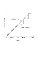
図5は、光電変換装置に入射される光の輝度とそれに対応するデジタルデータを説明する図面である。 FIG. 5 is a drawing illustrating the brightness of light incident on the photoelectric conversion device and the corresponding digital data.
図5において、輝度X以上の輝度を高輝度、輝度X以下の輝度を低輝度とする。高輝度の光が入射するときに本実施形態を適用した場合のデジタルデータの変化を実線で示し、従来技術の場合のデジタルデータの変化は点線で示している。本実施形態を適用した場合も従来技術の場合も、低輝度領域におけるAD変換の分解能は等しい。 In FIG. 5, the luminance of the luminance X or more is defined as the high luminance, and the luminance of the luminance X or less is defined as the low luminance. The change in digital data when the present embodiment is applied when high-luminance light is incident is shown by a solid line, and the change in digital data in the case of the prior art is shown by a dotted line. The resolution of the AD conversion in the low-luminance region is the same regardless of whether the present embodiment is applied or the prior art.
図5では図3(B)、図4と同様、高輝度領域でカウンタ回路の下位2ビットをゲーティングするものとする。カウンタ回路の下位2ビットをゲーティングするので、高輝度領域において、点線での4階調分の輝度の変化が実線の1階調分の輝度の変化になる。 In FIG. 5, as in FIGS. 3 (B) and 4, it is assumed that the lower two bits of the counter circuit are gated in the high luminance region. Since the lower two bits of the counter circuit are gated, the change in the luminance for four gradations on the dotted line becomes the change in the luminance for one gradation on the solid line in the high luminance region.
一般的に、撮影された画像において、高輝度よりも低輝度の方が輝度の変化に対する視認性が高い。したがって、分解能の変化を視認されにくい高輝度領域であれば分解能を小さくしても画質への影響は小さい。よって、本実施形態を適用すれば、画質に与える影響を抑えて消費電力低減を実現できる。 Generally, in a captured image, low brightness has higher visibility to change in brightness than high brightness. Therefore, in the high-luminance region where the change in resolution is difficult to see, even if the resolution is reduced, the effect on the image quality is small. Therefore, if this embodiment is applied, it is possible to reduce the power consumption by suppressing the influence on the image quality.
本実施形態は、輝度領域を2以上の任意の領域に細分化し、それぞれの輝度領域で異なる分解能を設定することも可能である。輝度領域の分け方や分解能は求められる画質によって設定することができる。 In the present embodiment, it is also possible to subdivide the luminance region into two or more arbitrary regions and set different resolutions in each luminance region. The method of dividing the luminance region and the resolution can be set according to the required image quality.
図5では輝度の領域を低輝度と高輝度の2種類に分けて分解能を切り替えたが、図6では輝度の領域を低輝度、中輝度、高輝度の3つにわけ、それぞれの領域で異なる分解能を設定している。 In FIG. 5, the brightness region is divided into two types, low brightness and high brightness, and the resolution is switched. However, in FIG. 6, the brightness region is divided into three types, low brightness, medium brightness, and high brightness, and each area is different. The resolution is set.
図6では、中輝度以上の輝度領域で、入射光が低輝度のときから分解能を変更しない場合のデジタルデータの変化を点線で示し、分解能を変更する場合のデジタルデータの変化を実線で記載している。この例では中輝度領域ではカウンタ回路の下位2ビット、高輝度の領域ではカウンタ回路の下位3ビットをゲーティングし、ゲーティングしたビットが動作しないようにしている。よって中輝度領域での1階調の変化は、低輝度領域での4階調分の変化に相当し、高輝度領域での1階調分の変化は低輝度領域での8階調分の変化に相当する。 In FIG. 6, in the luminance region of medium brightness or higher, the change in digital data when the resolution is not changed from the time when the incident light is low brightness is shown by a dotted line, and the change in digital data when the resolution is changed is shown by a solid line. ing. In this example, the lower 2 bits of the counter circuit are gated in the medium-luminance region, and the lower 3 bits of the counter circuit are gated in the high-luminance region so that the gated bits do not operate. Therefore, the change of one gradation in the medium-luminance region corresponds to the change of four gradations in the low-luminance region, and the change of one gradation in the high-luminance region is equivalent to the change of eight gradations in the low-luminance region. Corresponds to change.
これまで、カウンタ回路7に一般的なグレイコードカウンタを用いる場合について説明してきたが、図7に示すタイミングチャートのような動作をするカウンタにも本実施形態は適用可能である。
Although a case where a general Gray code counter is used for the
図7に示したタイミングチャートでは、1ビット目にあたる信号を位相の異なる2つの信号1ビットAと1ビットBとにおきかえている。2ビット目以降は一般的なグレイコードカウンタと同じ動作である。位相の異なる信号1ビットAと1ビットBとは、比較回路3の出力の反転に応じたレベルを列メモリにそのまま格納する。演算処理回路8の演算処理で、列メモリ4に記憶された1ビットAと1ビットBの排他的論理和(EXOR)を得る処理を行うことで、1ビット目の信号を生成することができる。図7に示したタイミングチャートのような動作は、例えばカウンタ回路の動作周波数が早く、回路動作が困難な場合などで好適に使用できる。
In the timing chart shown in FIG. 7, the signal corresponding to the first bit is replaced with two signals having different phases, 1 bit A and 1 bit B. The operation after the second bit is the same as that of a general Gray code counter. The
図7では最下位ビットである1ビット目のみを位相の異なる信号で代用する構成を説明したが、本実施形態はそれに限定されない。複数ビットを複数の位相の異なる信号でおきかえて、演算処理で該複数ビットを生成してもよい。 Although FIG. 7 has described a configuration in which only the first bit, which is the least significant bit, is substituted with a signal having a different phase, the present embodiment is not limited thereto. A plurality of bits may be replaced with a plurality of signals having different phases, and the plurality of bits may be generated by arithmetic processing.
また、これまで、カウンタ回路7の出力にゲーティング部12を接続し、ゲーティング部12で複数ビットの動作を停止していたが、本実施形態はそれに限定されない。例えば、カウンタ回路7内で、下位複数ビットのカウント動作を停止する構成であってもよい。その場合は、ゲーティング部12を配置する必要はない。
Further, until now, the
図8に示すタイミングチャートは、カウンタ回路7に周波数の高いクロックCLK1と周波数の低いクロックCLK2とを供給する例である。
The timing chart shown in FIG. 8 is an example of supplying the high frequency clock CLK1 and the low frequency clock CLK2 to the
図8のタイミングチャートでは、図3同様にカウンタ回路7のKビット目がLowからHighに遷移する時刻Tjを境に低輝度領域と高輝度領域とを分けている。カウンタ回路7は、低輝度領域ではCLK1に同期してカウント動作を行い、高輝度領域ではCLK2に同期してカウント動作を行っている。なお、図8の例ではCLK2の周波数はCLK1の周波数の1/2であり、カウンタ回路7はグレイコードカウンタである。
In the timing chart of FIG. 8, as in FIG. 3, the low-luminance region and the high-luminance region are separated at the time Tj at which the K-th bit of the
この構成では、時刻Tj以前にAD変換が終了した場合はそのまま演算処理を行い、得られたカウント値に対応するデジタルデータを得ることができる。 In this configuration, if the AD conversion is completed before the time Tj, the arithmetic processing can be performed as it is, and the digital data corresponding to the obtained count value can be obtained.
一方時刻Tj以後にAD変換が終了する場合は、1ビット目からK-1ビット目のカウント値に対応するデジタルデータを2倍にした値と、Kビット目の値2^(K-1)とを足すことで、分解能が小さくなったKビットのデジタルデータを得ることができる。
On the other hand, when the AD conversion ends after the time Tj, the value obtained by doubling the digital data corresponding to the count value from the first bit to the K-1 bit and the value of the
図8に示した例では、高輝度領域でカウンタ回路7の動作周波数が低くなり、カウンタ回路7の後段に接続されるバッファ部13の動作周波数も低くなるので、これまでと同様に消費電力の低減が可能である。
In the example shown in FIG. 8, the operating frequency of the
なお、図8のタイミングチャートの場合、カウンタ回路7の内部で分解能を小さくするので、ゲーティング部12を配する必要はない。
In the case of the timing chart of FIG. 8, since the resolution is reduced inside the
ここまでカウンタ回路7をグレイコードカウンタとして説明してきたが、カウンタ回路7はグレイコードカウンタに限定されず、例えば、適用できるならばバイナリカウンタであってもよい。全列の列メモリに対して、カウンタ回路7を一つとしたが、複数の列メモリごとにカウンタ回路7を配置してもよい。
Although the
また、高輝度側になると、下位ビットがLowに固定されるものとして説明したが、本実施形態はそれに限定されない。例えばHighに固定してもよいし、可能ならば中間電位に固定してもよい。 Further, although it has been described that the lower bits are fixed to Low on the high luminance side, the present embodiment is not limited thereto. For example, it may be fixed at High, or if possible, it may be fixed at an intermediate potential.
カウンタ回路7の出力のうち、ある1ビットの信号でゲーティングしたが、本実施形態はそれに限定されない。複数ビットの信号を用いて、ゲート信号を生成してもよい。
Of the outputs of the
本実施形態では、時刻Tj以前を第1の期間、時刻Tj以後を第2の期間とし、第1の期間と第2の期間とを連続した期間として説明したが、例えば第1の期間の経過後第2の期間の開始までの間にカウンタを休止させる第3の期間が存在してもかまわない。 In the present embodiment, the period before the time Tj is defined as the first period, the period after the time Tj is defined as the second period, and the first period and the second period are described as continuous periods. There may be a third period in which the counter is paused before the start of the second period.
[第二の実施形態]
本実施形態について図9から図12を用いて説明する。
[Second embodiment]
This embodiment will be described with reference to FIGS. 9 to 12.
図9は本実施形態における光電変換装置を説明する図面である。図9における各番号のうち図2と同一のものには同一符号を付してあるため説明を省略し、主として第一の実施形態と異なる部分を説明する。 FIG. 9 is a drawing illustrating a photoelectric conversion device according to the present embodiment. Of the numbers in FIG. 9, the same numbers as those in FIG. 2 are designated by the same reference numerals, and therefore the description thereof will be omitted, and the parts different from those of the first embodiment will be mainly described.
図9の光電変換装置では、図1のカウンタ回路7と列メモリ4が、CLK生成回路90と列カウンタ部91に変更されている。
In the photoelectric conversion device of FIG. 9, the
列カウンタ部91には高周波数のクロックが伝搬するCLK配線92と低周波数のクロックが伝搬するCLK配線93とが接続される。CLK配線92、93には複数列ごとにクロックバッファ回路94が配置されている。
The
図10に、本実施形態におけるAD変換動作のタイミングチャートを示す。 FIG. 10 shows a timing chart of the AD conversion operation in the present embodiment.
図2で説明した箇所については、詳細な説明を省略する。図2と同様に、入射光の輝度が高くなれば、読み出し回路2の処理により画素信号の電位も大きくなるものとする。また、比較回路3の出力はランプ信号の電位が画素信号より大きいとき、Lowになるものとする。
Detailed description of the parts described with reference to FIG. 2 will be omitted. Similar to FIG. 2, as the brightness of the incident light increases, the potential of the pixel signal also increases due to the processing of the
時刻T100で制御信号RAMP_ENおよび制御信号CNT_ENがLowからHighに遷移し、電位が時間によって変化するランプ信号の出力が開始されるとともに、列カウンタ部91はカウント動作を開始する。
At time T100, the control signal RAMP_EN and the control signal CNT_EN transition from Low to High, the output of the lamp signal whose potential changes with time is started, and the
時刻T101になると、比較回路3に入力されるランプ信号と画素信号との電位の大小関係が反転し、比較回路3の出力がHighからLowに遷移する。このタイミングで列カウンタ部91のカウント動作を終了し、その時のカウント値M(Mは整数)を保持することで、AD変換を実現する。その後、演算処理回路にデータを転送し、演算処理を行う。
At time T101, the magnitude relationship between the potentials of the lamp signal and the pixel signal input to the
図11は本実施形態における列カウンタ部91の動作を説明するタイミングチャートである。
FIG. 11 is a timing chart illustrating the operation of the
高周波数のクロックをCLK_F、低周波数のクロックをCLK_Sとし、列カウンタ部91をバイナリカウンタとしている。図11ではCLK_Sの周波数をCLK_Fの周波数の1/2としている。カウンタのKビット目がLowからHighに遷移する時刻Tjより前に比較回路3の出力が反転する場合の輝度低輝度、時刻Tjより後に比較回路3の出力が反転する場合の輝度は高輝度としている。
The high frequency clock is CLK_F, the low frequency clock is CLK_S, and the
列カウンタ部に入力される2つのクロックのうち、入射光が低輝度領域に属する輝度の場合はカウンタ部91をCLK_Fに同期してカウント動作がされる。高輝度領域に属する輝度の光が入射する場合はカウンタ部91をCLK_Sに同期してカウント動作がなされる。
Of the two clocks input to the column counter unit, when the incident light has a luminance belonging to the low luminance region, the
時刻Tjより前にAD変換が終了した場合は、保持されたカウント値がそのままデジタルデータとなる。時刻Tj後にAD変換が終了する場合は、1ビット目からK-1ビット目に対応するデジタルデータを2倍にした値と、Kビット目の値2^(K-1)とを足せば、分解能が小さくなったKビットのデジタルデータを得ることができる。
If the AD conversion is completed before the time Tj, the held count value becomes digital data as it is. When the AD conversion ends after the time Tj, the value obtained by doubling the digital data corresponding to the 1st bit to the K-1 bit and the
図12は図11に示したタイミングチャートの動作を実現する列カウンタ部91の一例である。
FIG. 12 is an example of the
列カウンタ部91は列カウンタ回路121と、クロックゲート回路122とで構成される。
The
クロックゲート回路122はマルチプレクサMUXと2入力のAND回路123、124とで構成される。
The
AND回路123には信号CNT_ENと比較回路出力が入力される。
The signal CNT_EN and the comparison circuit output are input to the AND
マルチプレクサMUXには高周波クロックCLK_Fと低周波クロックCLK_Sとが入力され、さらに制御入力として列カウンタ回路121のKビット目の出力が入力される。マルチプレクサMUXは列カウンタ回路121のKビット目がLowの時はCLK_Fを出力し、Highの時はCLK_Sを出力する。
The high frequency clock CLK_F and the low frequency clock CLK_S are input to the multiplexer MUX, and the output of the K bit of the
AND回路124の入力には、マルチプレクサMUXの出力とAND回路123の出力とが入力され、AND回路124を介して列カウンタ回路121に動作用クロックが供給される。
The output of the multiplexer MUX and the output of the AND
図12の回路より、比較回路出力がHighかつ、信号CNT_ENがHighで、列カウンタ回路121のKビット目がLowの時にCLK_Fが列カウンタ部91に供給される。
From the circuit of FIG. 12, CLK_F is supplied to the
一方、比較回路出力がHighかつ、信号CNT_ENがHighで、列カウンタ回路121のKビット目がHighの時にはCLK_Sが列カウンタ部91に供給される。
On the other hand, when the comparison circuit output is High, the signal CNT_EN is High, and the K bit of the
なお、図12に示した回路は列カウンタ部91の一例であり、構成を限定するものではない。
The circuit shown in FIG. 12 is an example of the
以上の説明より、列カウンタ部を有する光電変換装置においても、ある輝度以上の光について分解能を小さくすることで光電変換装置の消費電力低減が可能である。また、前述の通り、輝度の変化が視認されにくい高輝度領域で分解能を小さくするので、画質への影響は小さい。 From the above description, even in a photoelectric conversion device having a column counter unit, it is possible to reduce the power consumption of the photoelectric conversion device by reducing the resolution for light having a certain luminance or higher. Further, as described above, since the resolution is reduced in the high luminance region where the change in luminance is hard to be visually recognized, the influence on the image quality is small.
これまで、列カウンタ部に2種類のクロックが入力されるものとして説明したが、本実施形態はそれに限定されない。例えば、1種類のクロックのみを列カウンタ部に入力し、もう1種類のクロックを列カウンタ部内で生成してもよい。また、3種類以上のクロックを列カウンタ部に入力してもよい。例えば3種類のクロックを用いれば、図6に示したように輝度領域を低輝度領域、中輝度領域、高輝度領域にわけ、それぞれの領域で分解能を設定することが可能である。 So far, it has been described that two types of clocks are input to the column counter unit, but the present embodiment is not limited thereto. For example, only one type of clock may be input to the column counter unit, and another type of clock may be generated in the column counter unit. Further, three or more kinds of clocks may be input to the column counter unit. For example, if three types of clocks are used, as shown in FIG. 6, the luminance region is divided into a low-luminance region, a medium-luminance region, and a high-luminance region, and the resolution can be set in each region.
本実施例では列カウンタ回路121の出力のうちある1ビットの信号でゲーティングしたが、複数ビットの信号を用いて、ゲート信号を生成してもよい。
In this embodiment, gating is performed with a signal of one bit out of the output of the
[第三の実施形態]
本実施形態について図13~図15を用いて説明する。
[Third embodiment]
This embodiment will be described with reference to FIGS. 13 to 15.
図13は本実施形態における光電変換装置を示した図面である。これまでに説明した箇所については詳細な説明を省略し、主として第一及び第二の実施形態と異なる部分を説明する。 FIG. 13 is a drawing showing a photoelectric conversion device according to this embodiment. The detailed description of the parts described so far will be omitted, and the parts different from the first and second embodiments will be mainly described.
図13に示す光電変換装置は、画素アレイの列ごとに列メモリ131と列カウンタ部132を備える。列メモリ131には、バッファ回路133を介して、共通カウンタ部130で生成されるIビット(Iは整数)のカウント値CNT[I-1:0]を入力する。列カウンタ部132にはIビットのカウント値のうち最上位ビットの信号CNT[I-1]が入力される。
The photoelectric conversion device shown in FIG. 13 includes a
AD変換が開始されるとともに共通カウンタ部130が動作を開始する。列カウンタ部132は、共通カウンタ部130で生成される信号CNT[I-1]の入力されるパルス数をカウントする。ランプ信号と画素信号の電位の大小関係が反転し、比較回路3の出力が反転すると、列メモリ131はカウント値CNT[I-1:0]を記憶する。また、列カウンタ部132はカウント動作を停止し、自身でカウントしている値を保持する。
At the same time as the AD conversion is started, the
図13の例では、AD変換されたデジタルデータのうち、下位ビットは共通カウンタ部130のカウント値から生成され、上位ビットは列カウンタ部132のカウント値から生成される。AD変換が終了すると、列メモリ131に記憶された下位ビットのデータと、列カウンタ部132で保持されている上位ビットのデータとが演算処理回路8に伝搬され、演算処理がなされてデジタルデータが生成される。
In the example of FIG. 13, among the AD-converted digital data, the lower bits are generated from the count value of the
図14は図13の光電変換装置に本実施形態を適用した場合の、共通カウンタ部130および列カウンタ部132の動作を説明するタイミングチャートである。説明を簡単にするために、共通カウンタ部130はバイナリカウンタによってカウント値を生成するものとする。
FIG. 14 is a timing chart illustrating the operation of the
本実施形態では、デジタルデータの下位4ビットを共通カウンタ部130でカウントし、残りの上位ビットを列カウンタ部132でカウントする。列カウンタ部132に入力されるクロックは、共通カウンタ部130から出力される4ビット目の信号の反転信号である。よって、列カウンタ部132は共通カウンタ部130から出力される4ビット目の立下りエッジに同期して動作する。時刻TjでKビット目がHighになり、その信号で下位2ビットを固定する。時刻Tj以降ではAD変換終了まで下位2ビットはLowに固定されている。
In the present embodiment, the lower 4 bits of the digital data are counted by the
図15は図14に示したタイミングチャートの動作を実現する共通カウンタ部130の一例である。
FIG. 15 is an example of the
図15の例では、共通カウンタ部130はKビットのカウンタ回路150、インバータ回路151、4つのAND回路152で構成される。カウンタ回路150はKビットカウンタであるが、共通カウンタ部130からは下位4ビットのみが出力される。
In the example of FIG. 15, the
カウンタ回路150のKビット目がHighになると、インバータ回路151によりLowに反転された信号が、1、2ビット目のAND回路に入力される。よって、Kビット目がHighになった時刻Tj以降では1、2ビット目の出力はLowに固定される。3、4ビット目のAND回路152にはHighが入力されているため、3、4ビット目は時刻Tj以降もそのまま共通カウンタ部130から出力される。共通カウンタ部130からは下位4ビットのみが出力されるが、Kビット目の信号を下位2ビットのゲート信号として使用するため、カウンタ回路150をKビットカウンタとしている。なお、3、4ビット目をゲートする必要はないが、出力する4ビットすべてで遅延量をそろえるために、3、4ビット目にもAND回路152を配置している。
When the K-th bit of the
以上説明してきた通り、本実施形態では高輝度領域で共通カウンタ部130の下位ビットをLowに固定することで、ゲートされた下位ビットのバッファ回路133が動作しなくなり、その分の消費電力の低減が実現できる。前述の通り、分解能が小さくなるのは輝度の変化が視認されにくい高輝度領域なので、画質への影響は小さい。よって本実施形態を適用すれば、画質低下を抑制しつつ、消費電力の低減が可能となる。
As described above, in the present embodiment, by fixing the lower bits of the
本実施形態では共通カウンタ部130ではバイナリカウンタでカウント値を生成されるとしたが、本実施形態はそれに限定されない。例えば、グレイコードカウンタであってもよい。
In the present embodiment, the
カウンタ回路150をKビットとしたが、例えば、4ビットのカウンタとし、Kビット目の信号を列カウンタ部132から共通カウンタ部130に供給し、その信号をゲート信号として使用してもよい。
Although the
図15のタイミングチャートでは下位2ビットをゲートするものとして説明したが、下位1ビットでもよいし、3ビット以上であってもよい。また、図7のタイミングチャートで説明したように、複数の信号の位相をずらすことで、下位ビットの信号を生成してもよい。 In the timing chart of FIG. 15, the lower 2 bits are gated, but the lower 1 bit may be used, or 3 or more bits may be used. Further, as described in the timing chart of FIG. 7, the signals of the lower bits may be generated by shifting the phases of the plurality of signals.
本実施形態では、下位ビットをゲートする構成で説明したが、これまでにも説明したように、低輝度領域と高輝度領域でカウンタの動作周波数が異なる構成であってもよい。 In the present embodiment, the configuration in which the lower bits are gated has been described, but as described above, the counter may have different operating frequencies in the low-luminance region and the high-luminance region.
カウンタ回路150のある1ビットの信号でカウンタをゲーティングしたが、本実施形態はそれに限定されない。複数ビットの信号を用いて、ゲート信号を生成してもよい。また、列カウンタ部132の出力の複数ビットを用いてゲート信号を生成してもよい。
The counter is gated with a 1-bit signal of the
以上第一の実施形態から第三の実施形態までの説明では、読み出し回路から出力される画素信号は入射される光の輝度に応じて、電位が大きくなるものとして説明したが、本実施形態はそれに限定されない。輝度に応じて、電位が小さくなる構成であってもよい。読み出し回路に、入力信号にゲインをかけられるアンプを配置してもよい。その際アンプは反転アンプでも、非反転アンプでもよい。 In the above description from the first embodiment to the third embodiment, it has been described that the pixel signal output from the readout circuit has a higher potential according to the brightness of the incident light, but the present embodiment has been described. Not limited to that. The potential may be reduced depending on the brightness. An amplifier that can apply a gain to the input signal may be arranged in the read circuit. At that time, the amplifier may be an inverting amplifier or a non-inverting amplifier.
第一の実施形態から第三の実施形態までの説明では、下位ビットのゲートや、AD変換に用いるカウンタの動作周波数の変更に、該カウンタの出力信号を用いていたが、本実施形態はそれに限定されない。例えば、前記カウンタ以外に時間計測手段を持ち、該時間計測手段で生成される信号で、あるビットをゲートする、もしくは前記カウンタの動作周波数を変更する構成であってもよい。 In the description from the first embodiment to the third embodiment, the output signal of the counter is used for changing the gate of the lower bit and the operating frequency of the counter used for AD conversion, but this embodiment uses it. Not limited. For example, a time measuring means may be provided in addition to the counter, and a signal generated by the time measuring means may be configured to gate a certain bit or change the operating frequency of the counter.
なお、前述したデジタルCDSを行うために、画素のリセット信号と画素信号のそれぞれでAD変換を行うが、本実施形態は画素信号のAD変換時により好適に使用できる。 In order to perform the above-mentioned digital CDS, AD conversion is performed for each of the pixel reset signal and the pixel signal, but this embodiment can be more preferably used at the time of AD conversion of the pixel signal.
また、焦点距離検出機能を有する光電変換装置において、画素から焦点距離検出用の第1の信号と、画像情報用の第2の信号とをそれぞれ読み出す技術が知られている。本実施形態はそのような技術にも好適に適用できる。焦点距離検出用の第1の信号を読み出す第一の画素群と、画像情報用の第2の信号を読み出す第二の画素群を有する光電変換装置を例に挙げる。このような光電変換装置において、例えば画像情報である第2の信号の低輝度領域において分解能を大きく、高輝度領域において分解能を小さくすることが可能である。焦点距離検出用である第1の信号は、画像情報として使用しないことから第2の信号ほどの分解能は必要がない場合も考えられる。その場合は第1の信号の分解能を第2の信号の分解能よりも小さくすることが可能となる。 Further, in a photoelectric conversion device having a focal length detection function, there is known a technique of reading out a first signal for focal length detection and a second signal for image information from pixels. The present embodiment is also suitably applicable to such techniques. An example is a photoelectric conversion device having a first pixel group for reading a first signal for focal length detection and a second pixel group for reading a second signal for image information. In such a photoelectric conversion device, for example, it is possible to increase the resolution in the low-luminance region of the second signal which is image information and decrease the resolution in the high-luminance region. Since the first signal for detecting the focal length is not used as image information, it may be possible that the resolution as high as that of the second signal is not required. In that case, the resolution of the first signal can be made smaller than the resolution of the second signal.
以上のように、入射される光の輝度に応じて第1の信号、第2の信号のそれぞれの分解能を設定することで、焦点距離検出機能を有する光電変換装置においても消費電力の低減が可能である。 As described above, by setting the resolutions of the first signal and the second signal according to the brightness of the incident light, it is possible to reduce the power consumption even in the photoelectric conversion device having the focal length detection function. Is.
本実施形態は撮影モードごとに適用可否を設定できる。例えば高い画質が必要な静止画撮影モードにおいては輝度によらず分解能を一定とし、動画撮影モードにおいては、輝度によって分解能を設定することが可能である。また、各撮影モードにおいて、輝度領域とその領域における分解能をそれぞれで設定することも可能である。 Applicability of this embodiment can be set for each shooting mode. For example, in the still image shooting mode that requires high image quality, the resolution can be set to be constant regardless of the brightness, and in the moving image shooting mode, the resolution can be set by the brightness. It is also possible to set the luminance region and the resolution in the region in each shooting mode.
なお、各実施例における光電変換装置は図16に示すような積層型の構成をとっても構わない。 The photoelectric conversion device in each embodiment may have a laminated structure as shown in FIG.
図16に示した積層構造の光電変換装置は画素基板300と、回路基板310を有する。画素基板300には少なくとも画素部1が配される。回路基板には比較回路3、列メモリ4、ランプ源6、カウンタ回路7といった回路部が配されるが、回路の配置は回路基板上に限られず、例えば画素基板300にランプ源6やその他の回路を配してもよい。各回路はその一部を画素基板300に配し、他の一部を回路基板301に配してもよい。図16では2枚の基板からなる積層構造を示したが、例えばさらに回路を分割するか、回路や機能を追加するなどして3枚以上の基板からなる積層構造にしてもよい。
The photoelectric conversion device having a laminated structure shown in FIG. 16 has a
[第四の実施形態]
本実施形態による光電変換システムについて、図17を用いて説明する。図17は、本実施形態による光電変換システムの概略構成を示すブロック図である。
[Fourth Embodiment]
The photoelectric conversion system according to this embodiment will be described with reference to FIG. FIG. 17 is a block diagram showing a schematic configuration of a photoelectric conversion system according to the present embodiment.
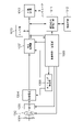
上記第1~第3実施形態で述べた光電変換装置(撮像装置)は、種々の光電変換システムに適用可能である。適用可能な光電変換システムの例としては、デジタルスチルカメラ、デジタルカムコーダ、監視カメラ、複写機、ファックス、携帯電話、車載カメラ、観測衛星などが挙げられる。また、レンズなどの光学系と撮像装置とを備えるカメラモジュールも、光電変換システムに含まれる。図17には、これらのうちの一例として、デジタルスチルカメラのブロック図を例示している。 The photoelectric conversion device (imaging device) described in the first to third embodiments is applicable to various photoelectric conversion systems. Examples of applicable photoelectric conversion systems include digital still cameras, digital camcorders, surveillance cameras, copiers, fax machines, mobile phones, in-vehicle cameras, observation satellites, and the like. A camera module including an optical system such as a lens and an image pickup device is also included in the photoelectric conversion system. FIG. 17 illustrates a block diagram of a digital still camera as an example of these.
図17に例示した光電変換システムは、光電変換装置の一例である撮像装置1004、被写体の光学像を撮像装置1004に結像させるレンズ1002を有する。さらに、レンズ1002を通過する光量を可変にするための絞り1003、レンズ1002の保護のためのバリア1001を有する。レンズ1002及び絞り1003は、撮像装置1004に光を集光する光学系である。撮像装置1004は、上記のいずれかの実施形態の光電変換装置(撮像装置)であって、レンズ1002により結像された光学像を電気信号に変換する。
The photoelectric conversion system illustrated in FIG. 17 includes an
光電変換システムは、また、撮像装置1004より出力される出力信号の処理を行うことで画像を生成する画像生成部である信号処理部1007を有する。信号処理部1007は、必要に応じて各種の補正、圧縮を行って画像データを出力する動作を行う。信号処理部1007は、撮像装置1004が設けられた半導体基板に形成されていてもよいし、撮像装置1004とは別の半導体基板に形成されていてもよい。
The photoelectric conversion system also has a
光電変換システムは、更に、画像データを一時的に記憶するためのメモリ部1010、外部コンピュータ等と通信するための外部インターフェース部(外部I/F部)1013を有する。更に光電変換システムは、撮像データの記録又は読み出しを行うための半導体メモリ等の記録媒体1012、記録媒体1012に記録又は読み出しを行うための記録媒体制御インターフェース部(記録媒体制御I/F部)1011を有する。なお、記録媒体1012は、光電変換システムに内蔵されていてもよく、着脱可能であってもよい。
The photoelectric conversion system further includes a
更に光電変換システムは、各種演算とデジタルスチルカメラ全体を制御する全体制御・演算部1009、撮像装置1004と信号処理部1007に各種タイミング信号を出力するタイミング発生部1008を有する。ここで、タイミング信号などは外部から入力されてもよく、光電変換システムは少なくとも撮像装置1004と、撮像装置1004から出力された出力信号を処理する信号処理部1007とを有すればよい。
Further, the photoelectric conversion system has a general control /
撮像装置1004は、撮像信号を信号処理部1007に出力する。信号処理部1007は、撮像装置1004から出力される撮像信号に対して所定の信号処理を実施し、画像データを出力する。光電変換システムは、この画像データを用いて、画像を生成する。
The
このように、本実施形態によれば、上記のいずれかの実施形態の光電変換装置(撮像装置)を適用した光電変換システムを実現することができる。 As described above, according to the present embodiment, it is possible to realize a photoelectric conversion system to which the photoelectric conversion device (imaging device) of any of the above embodiments is applied.
[第五の実施形態]
本実施形態の光電変換システム及び移動体について、図18を用いて説明する。図18は、本実施形態の光電変換システム及び移動体の構成を示す図である。
[Fifth Embodiment]
The photoelectric conversion system and the moving body of the present embodiment will be described with reference to FIG. FIG. 18 is a diagram showing a configuration of a photoelectric conversion system and a moving body of the present embodiment.
図18(a)は、車載カメラに関する光電変換システムの一例を示したものである。光電変換システム300は、撮像装置310を有する。撮像装置310は、上記のいずれかの実施形態に記載の光電変換装置(撮像装置)である。光電変換システム300は、撮像装置310により取得された複数の画像データに対し、画像処理を行う画像処理部312と、光電変換システム300により取得された複数の画像データから視差(視差画像の位相差)の算出を行う視差取得部314を有する。また、光電変換システム300は、算出された視差に基づいて対象物までの距離を算出する距離取得部316と、算出された距離に基づいて衝突可能性があるか否かを判定する衝突判定部318と、を有する。ここで、視差取得部314や距離取得部316は、対象物までの距離情報を取得する距離情報取得手段の一例である。すなわち、距離情報とは、視差、デフォーカス量、対象物までの距離等に関する情報である。衝突判定部318はこれらの距離情報のいずれかを用いて、衝突可能性を判定してもよい。距離情報取得手段は、専用に設計されたハードウェアによって実現されてもよいし、ソフトウェアモジュールによって実現されてもよい。また、FPGA(Field Programmable Gate Array)やASIC(Application Specific Integrated Circuit)等によって実現されてもよいし、これらの組合せによって実現されてもよい。
FIG. 18A shows an example of a photoelectric conversion system related to an in-vehicle camera. The
光電変換システム300は車両情報取得装置320と接続されており、車速、ヨーレート、舵角などの車両情報を取得することができる。また、光電変換システム300は、衝突判定部318での判定結果に基づいて、車両に対して制動力を発生させる制御信号を出力する制御装置である制御部ECU330が接続されている。また、光電変換システム300は、衝突判定部318での判定結果に基づいて、ドライバーへ警報を発する警報装置340とも接続されている。例えば、衝突判定部318の判定結果として衝突可能性が高い場合、制御部ECU330はブレーキをかける、アクセルを戻す、エンジン出力を抑制するなどして衝突を回避、被害を軽減する車両制御を行う。警報装置340は音等の警報を鳴らす、カーナビゲーションシステムなどの画面に警報情報を表示する、シートベルトやステアリングに振動を与えるなどしてユーザに警告を行う。
The
本実施形態では、車両の周囲、例えば前方又は後方を光電変換システム300で撮像する。図18(b)に、車両前方(撮像範囲350)を撮像する場合の光電変換システムを示した。車両情報取得装置320が、光電変換システム300ないしは撮像装置310に指示を送る。このような構成により、測距の精度をより向上させることができる。
In the present embodiment, the periphery of the vehicle, for example, the front or the rear, is imaged by the
上記では、他の車両と衝突しないように制御する例を説明したが、他の車両に追従して自動運転する制御や、車線からはみ出さないように自動運転する制御などにも適用可能である。更に、光電変換システムは、自車両等の車両に限らず、例えば、船舶、航空機あるいは産業用ロボットなどの移動体(移動装置)に適用することができる。加えて、移動体に限らず、高度道路交通システム(ITS)等、広く物体認識を利用する機器に適用することができる。 In the above, an example of controlling so as not to collide with another vehicle has been described, but it can also be applied to control for automatically driving following other vehicles and control for automatically driving so as not to go out of the lane. .. Further, the photoelectric conversion system can be applied not only to a vehicle such as an own vehicle but also to a moving body (moving device) such as a ship, an aircraft or an industrial robot. In addition, it can be applied not only to moving objects but also to devices that widely use object recognition, such as intelligent transportation systems (ITS).
1 画素部
3 比較回路
6 ランプ源
7 カウンタ回路
12 ゲーティング部
1
Claims (20)
前記比較回路での前記比較処理に並行してカウント処理を行うカウンタ部と、を有し、
前記比較処理に応じたカウント値であるデジタルデータを取得することによって前記アナログ信号のアナログデジタル変換を行うアナログデジタル変換回路であって、
1つの前記アナログ信号のアナログデジタル変換の開始から終了までの期間に第1の期間および前記第1の期間の後の第2の期間が含まれ、前記第1の期間では前記カウント処理が高速に実行され、前記第2の期間では前記カウント処理が低速に実行されることを特徴とするアナログデジタル変換回路。 A comparison circuit that compares and processes analog signals and lamp signals,
It has a counter unit that performs counting processing in parallel with the comparison processing in the comparison circuit.
An analog-to-digital conversion circuit that performs analog-to-digital conversion of the analog signal by acquiring digital data that is a count value according to the comparison process.
The period from the start to the end of the analog-to-digital conversion of one analog signal includes a first period and a second period after the first period, and the counting process is performed at high speed in the first period. An analog-to-digital conversion circuit that is executed and the count process is executed at a low speed in the second period.
前記比較回路での前記比較処理に並行してカウント処理を行うカウンタ部と、を有し、
前記比較処理に応じたカウント値であるデジタルデータを取得することによって前記アナログ信号のアナログデジタル変換を行うアナログデジタル変換回路であって、
1つの前記アナログ信号のアナログデジタル変換の開始から終了までの期間に第1の期間および前記第1の期間の後の第2の期間が含まれ、
前記第1の期間では、第一の分解能で前記アナログデジタル変換回路が前記アナログデジタル変換を行い、
前記第2の期間では、前記第一の分解能よりも低い第二の分解能で前記アナログデジタル変換回路が前記アナログデジタル変換を行うことを特徴とするアナログデジタル変換回路。 A comparison circuit that compares and processes analog signals and lamp signals,
It has a counter unit that performs counting processing in parallel with the comparison processing in the comparison circuit.
An analog-to-digital conversion circuit that performs analog-to-digital conversion of the analog signal by acquiring digital data that is a count value according to the comparison process.
The period from the start to the end of the analog-to-digital conversion of one analog signal includes a first period and a second period after the first period.
In the first period, the analog-to-digital conversion circuit performs the analog-to-digital conversion at the first resolution.
The analog-to-digital conversion circuit, characterized in that, in the second period, the analog-to-digital conversion circuit performs the analog-to-digital conversion with a second resolution lower than the first resolution.
前記カウンタ部は前記比較回路での前記比較処理に並行してカウント処理を行うことによって前記カウント値を出力し、
前記比較処理に応じたカウント値であるデジタルデータを取得してアナログデジタル変換を行うアナログデジタル変換回路であって、
1つの前記アナログ信号のアナログデジタル変換の開始から終了までの期間に第1の期間および前記第1の期間の後の第2の期間が含まれ、
前記第1の期間において信号が変化する、前記複数ビットの最下位ビット側から少なくとも1ビットが、前記第2の期間においては所定の電位に固定される
ことを特徴とするアナログデジタル変換回路。 It includes a comparison circuit for comparing an analog signal and a lamp signal, and a counter unit for outputting a count value having a plurality of bits.
The counter unit outputs the count value by performing a count process in parallel with the comparison process in the comparison circuit.
An analog-to-digital conversion circuit that acquires digital data that is a count value according to the comparison process and performs analog-to-digital conversion.
The period from the start to the end of the analog-to-digital conversion of one analog signal includes a first period and a second period after the first period.
An analog-to-digital conversion circuit characterized in that at least one bit from the least significant bit side of the plurality of bits whose signal changes in the first period is fixed to a predetermined potential in the second period.
前記カウンタ部は前記比較回路での前記比較処理に並行してカウント処理を行い、
前記比較処理に応じたカウント値であるデジタルデータを取得してアナログデジタル変換を行うアナログデジタル変換回路であって、
1つの前記アナログ信号のアナログデジタル変換の開始から終了までの期間に第1の期間および前記第1の期間の後の第2の期間が含まれ、
前記第2の期間における前記カウンタ部の動作周波数が前記第1の期間における前記カウンタ部の動作周波数よりも小さいことを特徴とするアナログデジタル変換回路。 It has a comparison circuit that compares and processes analog signals and lamp signals, and a counter unit.
The counter unit performs a count process in parallel with the comparison process in the comparison circuit.
An analog-to-digital conversion circuit that acquires digital data that is a count value according to the comparison process and performs analog-to-digital conversion.
The period from the start to the end of the analog-to-digital conversion of one analog signal includes a first period and a second period after the first period.
An analog-to-digital conversion circuit characterized in that the operating frequency of the counter unit in the second period is smaller than the operating frequency of the counter unit in the first period.
前記カウンタ部の最下位ビットの出力と、前記インバータ回路を介した前記最上位ビットの出力とが入力される論理回路とを含むゲーティング部を有することを特徴とする、請求項1乃至請求項5のいずれか一項に記載のアナログデジタル変換回路。 An inverter circuit that inverts the output of the most significant bit of the counter unit,
1. 5. The analog-to-digital conversion circuit according to any one of 5.
前記カウンタ部の最上位ビットの出力がHighのときに出力されるクロックの周波数と、
前記カウンタ部の最上位ビットの出力がLowのときに出力されるクロックの周波数と、が異なるマルチプレクサを含むゲーティング部を有することを特徴とする、請求項1乃至請求項5のいずれか一項に記載のアナログデジタル変換回路。 A multiplexer in which a plurality of clocks having different frequencies are input and controlled by the output of the counter unit.
The frequency of the clock output when the output of the most significant bit of the counter unit is High, and
One of claims 1 to 5, wherein the counter unit has a gating unit including a multiplexer that is different from the frequency of the clock output when the output of the most significant bit is Low. The analog-to-digital conversion circuit described in.
前記アナログ信号は前記画素で生じる電荷に基づく信号であることを特徴とする光電変換装置。 It has a plurality of pixels and the analog-to-digital conversion circuit according to any one of claims 1 to 8.
A photoelectric conversion device characterized in that the analog signal is a signal based on the electric charge generated in the pixel.
前記カウンタ部は複数の前記列メモリにカウント値を供給する共通カウンタを含むことを特徴とする請求項9記載の光電変換装置。 The plurality of pixels are arranged in an array, and each row of the array is connected to a row memory.
The photoelectric conversion device according to claim 9, wherein the counter unit includes a common counter that supplies count values to a plurality of the column memories.
前記共通カウンタは前記カウント値のうち下位ビットの値を生成し、
前記列カウンタは前記カウント値のうち上位ビットの値を生成することを特徴とする請求項11記載の光電変換装置。 The count value has a plurality of bits and has a plurality of bits.
The common counter generates the value of the lower bit of the count value,
The photoelectric conversion device according to claim 11, wherein the column counter generates a value of a high-order bit among the count values.
前記第一の画素群は前記複数の画素を含み、
前記第二の画素群は前記複数の画素とは異なる画素を含み、
前記第二の画素群に含まれる前記画素で生じる電荷に基づくアナログ信号は、第三の分解能でデジタルデータに変換されることを特徴とする、請求項9乃至請求項12のいずれか1項に記載の光電変換装置。 The photoelectric conversion device has a first pixel group and a second pixel group.
The first pixel group includes the plurality of pixels.
The second pixel group includes pixels different from the plurality of pixels.
The invention according to any one of claims 9 to 12, wherein the analog signal based on the electric charge generated in the pixel included in the second pixel group is converted into digital data with a third resolution. The photoelectric conversion device described.
請求項9乃至請求項14のいずれか一項に記載の光電変換装置として動作する撮影モードを有することを特徴とする光電変換装置。 The photoelectric conversion device operates in a plurality of shooting modes and operates in a plurality of shooting modes.
A photoelectric conversion device having a photographing mode that operates as the photoelectric conversion device according to any one of claims 9 to 14.
前記半導体基板を含む複数の半導体基板を積層して構成されることを特徴とする請求項9乃至請求項15のいずれか一項に記載の光電変換装置。 The plurality of pixels are formed on a semiconductor substrate, and the plurality of pixels are formed on the semiconductor substrate.
The photoelectric conversion device according to any one of claims 9 to 15, wherein a plurality of semiconductor substrates including the semiconductor substrate are laminated.
前記光電変換装置が出力する信号を用いて画像を生成する信号処理部とを有することを特徴とする光電変換システム。 The photoelectric conversion device according to any one of claims 9 to 16.
A photoelectric conversion system including a signal processing unit that generates an image using a signal output by the photoelectric conversion device.
前記光電変換装置が出力する信号を用いて前記移動体の移動を制御する制御部を有することを特徴とする移動体。 A moving body including the photoelectric conversion device according to any one of claims 9 to 16.
A moving body having a control unit that controls the movement of the moving body by using a signal output by the photoelectric conversion device.
アナログ信号と、ランプ信号とを比較処理する比較回路と、
前記比較回路での前記比較処理に並行してカウント処理を行うカウンタ部と、を有し、
前記比較処理に応じたカウント値を保持することでデジタルデータを取得することによって前記アナログ信号のアナログデジタル変換を行うアナログデジタル変換回路を有し、
前記アナログ信号のアナログデジタル変換の開始から終了までの期間に第1の期間および前記第1の期間の後の第2の期間が含まれ、前記第1の期間では前記カウント処理が高速に実行され、前記第2の期間では前記カウント処理が低速に実行されることを特徴とする半導体基板。 A semiconductor substrate for stacking on another semiconductor substrate,
A comparison circuit that compares and processes analog signals and lamp signals,
It has a counter unit that performs counting processing in parallel with the comparison processing in the comparison circuit.
It has an analog-to-digital conversion circuit that performs analog-to-digital conversion of the analog signal by acquiring digital data by holding a count value corresponding to the comparison process.
The period from the start to the end of the analog-to-digital conversion of the analog signal includes a first period and a second period after the first period, and the counting process is executed at high speed in the first period. A semiconductor substrate, characterized in that the counting process is executed at a low speed in the second period.
アナログ信号と、ランプ信号とを比較処理する比較回路と、
前記比較回路での前記比較処理に並行してカウント処理を行うカウンタ部と、を有し、
前記比較処理に応じたカウント値を保持することでデジタルデータを取得することによって前記アナログ信号のアナログデジタル変換を行うアナログデジタル変換回路を有し、
1つの前記アナログ信号のアナログデジタル変換の開始から終了までの期間に第1の期間および前記第1の期間の後の第2の期間が含まれ、
前記第1の期間では、前記アナログデジタル変換回路が第一の分解能で前記アナログデジタル変換を行い、
前記第2の期間では、前記第一の分解能よりも低い第二の分解能として前記アナログデジタル変換回路が前記アナログデジタル変換を行うことを特徴とする半導体基板。 A semiconductor substrate for stacking on another semiconductor substrate,
A comparison circuit that compares and processes analog signals and lamp signals,
It has a counter unit that performs counting processing in parallel with the comparison processing in the comparison circuit.
It has an analog-to-digital conversion circuit that performs analog-to-digital conversion of the analog signal by acquiring digital data by holding a count value corresponding to the comparison process.
The period from the start to the end of the analog-to-digital conversion of one analog signal includes a first period and a second period after the first period.
In the first period, the analog-to-digital conversion circuit performs the analog-to-digital conversion with the first resolution.
A semiconductor substrate characterized in that, in the second period, the analog-to-digital conversion circuit performs the analog-to-digital conversion as a second resolution lower than the first resolution.
Priority Applications (2)
| Application Number | Priority Date | Filing Date | Title |
|---|---|---|---|
| JP2020184492A JP2022074445A (en) | 2020-11-04 | 2020-11-04 | Analog-to-digital conversion circuit, photoelectric conversion apparatus, and photoelectric conversion system |
| US17/516,010 US11627269B2 (en) | 2020-11-04 | 2021-11-01 | Analog-to-digital conversion circuit using comparator and counter, photoelectric conversion apparatus using comparator and counter, and photoelectric conversion system using comparator and counter |
Applications Claiming Priority (1)
| Application Number | Priority Date | Filing Date | Title |
|---|---|---|---|
| JP2020184492A JP2022074445A (en) | 2020-11-04 | 2020-11-04 | Analog-to-digital conversion circuit, photoelectric conversion apparatus, and photoelectric conversion system |
Publications (2)
| Publication Number | Publication Date |
|---|---|
| JP2022074445A true JP2022074445A (en) | 2022-05-18 |
| JP2022074445A5 JP2022074445A5 (en) | 2023-10-31 |
Family
ID=81379351
Family Applications (1)
| Application Number | Title | Priority Date | Filing Date |
|---|---|---|---|
| JP2020184492A Pending JP2022074445A (en) | 2020-11-04 | 2020-11-04 | Analog-to-digital conversion circuit, photoelectric conversion apparatus, and photoelectric conversion system |
Country Status (2)
| Country | Link |
|---|---|
| US (1) | US11627269B2 (en) |
| JP (1) | JP2022074445A (en) |
Family Cites Families (9)
| Publication number | Priority date | Publication date | Assignee | Title |
|---|---|---|---|---|
| US6885331B2 (en) * | 2003-09-15 | 2005-04-26 | Micron Technology, Inc. | Ramp generation with capacitors |
| JP4281822B2 (en) * | 2007-05-11 | 2009-06-17 | ソニー株式会社 | Solid-state imaging device, imaging device |
| JP2009177797A (en) * | 2007-12-26 | 2009-08-06 | Panasonic Corp | Solid-state imaging device and method of driving the same |
| JP5362080B2 (en) | 2011-10-07 | 2013-12-11 | キヤノン株式会社 | Solid-state imaging device and imaging system |
| JP5449290B2 (en) * | 2011-10-07 | 2014-03-19 | キヤノン株式会社 | Ramp signal output circuit, analog-digital conversion circuit, imaging device, and driving method of ramp signal output circuit |
| JP5893550B2 (en) * | 2012-04-12 | 2016-03-23 | キヤノン株式会社 | Imaging apparatus and imaging system |
| JP6395425B2 (en) * | 2014-04-11 | 2018-09-26 | キヤノン株式会社 | Imaging apparatus and imaging system |
| US10112531B2 (en) * | 2016-04-29 | 2018-10-30 | Ford Global Technologies, Llc | Vehicle badge with improved resolution |
| JP7116599B2 (en) * | 2018-06-11 | 2022-08-10 | キヤノン株式会社 | Imaging device, semiconductor device and camera |
-
2020
- 2020-11-04 JP JP2020184492A patent/JP2022074445A/en active Pending
-
2021
- 2021-11-01 US US17/516,010 patent/US11627269B2/en active Active
Also Published As
| Publication number | Publication date |
|---|---|
| US11627269B2 (en) | 2023-04-11 |
| US20220141414A1 (en) | 2022-05-05 |
Similar Documents
| Publication | Publication Date | Title |
|---|---|---|
| JP6882910B2 (en) | Solid-state image sensor, control method of solid-state image sensor, image pickup system and moving object | |
| US10834354B2 (en) | Imaging device, imaging system, movable object, and signal processing device | |
| JP6806553B2 (en) | Imaging device, driving method of imaging device and imaging system | |
| JP2021029017A (en) | Photoelectric conversion device, imaging system, mobile body, and exposure control device | |
| CN110611777B (en) | Image pickup apparatus, image pickup system, and mobile device | |
| JP2019179980A (en) | Solid-state imaging apparatus and driving method of the same | |
| US11218654B2 (en) | Photoelectric conversion device, imaging system, and movable body | |
| US11102435B2 (en) | Imaging device and method of driving imaging device | |
| JP2019047267A (en) | Solid state image sensor, imaging system, and mobile | |
| JP2022074445A (en) | Analog-to-digital conversion circuit, photoelectric conversion apparatus, and photoelectric conversion system | |
| JP2022100947A (en) | Photoelectric conversion device, photoelectric conversion system, and movable body | |
| JP2020096259A (en) | Photoelectric conversion device and imaging system | |
| JP7370767B2 (en) | AD conversion circuit, photoelectric conversion device, photoelectric conversion system, mobile object | |
| US11575868B2 (en) | Photoelectric conversion apparatus, method of driving photoelectric conversion apparatus, photoelectric conversion system, and moving body | |
| JP2017200062A (en) | Imaging apparatus, imaging system, and mobile | |
| JP2019009672A (en) | Imaging apparatus and driving method thereof | |
| JP2021097382A (en) | Imaging apparatus and imaging system | |
| JP2021002727A (en) | Photoelectric conversion device, photoelectric conversion system, and mobile body | |
| JP7336199B2 (en) | IMAGING DEVICE, IMAGING SYSTEM AND SIGNAL PROCESSING DEVICE | |
| JP7254576B2 (en) | Photoelectric conversion device, signal processing circuit, imaging system, moving body | |
| US20230188868A1 (en) | Photoelectric conversion apparatus and equipment | |
| JP7299711B2 (en) | Photoelectric conversion device and driving method thereof | |
| US20230179881A1 (en) | Photoelectric conversion device | |
| JP2023096467A (en) | Signal processing device | |
| JP2022089013A (en) | Photoelectric conversion device, photoelectric conversion system, movable body, semiconductor substrate, and method for driving photoelectric conversion device |
Legal Events
| Date | Code | Title | Description |
|---|---|---|---|
| RD01 | Notification of change of attorney |
Free format text: JAPANESE INTERMEDIATE CODE: A7421 Effective date: 20201209 |
|
| A521 | Request for written amendment filed |
Free format text: JAPANESE INTERMEDIATE CODE: A523 Effective date: 20231023 |
|
| A621 | Written request for application examination |
Free format text: JAPANESE INTERMEDIATE CODE: A621 Effective date: 20231023 |
|
| RD01 | Notification of change of attorney |
Free format text: JAPANESE INTERMEDIATE CODE: A7421 Effective date: 20231213 |