JP2022040101A - Radio frequency chip, baseband chip, and wlan device - Google Patents
Radio frequency chip, baseband chip, and wlan device Download PDFInfo
- Publication number
- JP2022040101A JP2022040101A JP2021139041A JP2021139041A JP2022040101A JP 2022040101 A JP2022040101 A JP 2022040101A JP 2021139041 A JP2021139041 A JP 2021139041A JP 2021139041 A JP2021139041 A JP 2021139041A JP 2022040101 A JP2022040101 A JP 2022040101A
- Authority
- JP
- Japan
- Prior art keywords
- radio frequency
- signal
- chip
- circuit
- circuits
- Prior art date
- Legal status (The legal status is an assumption and is not a legal conclusion. Google has not performed a legal analysis and makes no representation as to the accuracy of the status listed.)
- Granted
Links
Images


Classifications
-
- H—ELECTRICITY
- H04—ELECTRIC COMMUNICATION TECHNIQUE
- H04B—TRANSMISSION
- H04B1/00—Details of transmission systems, not covered by a single one of groups H04B3/00 - H04B13/00; Details of transmission systems not characterised by the medium used for transmission
- H04B1/005—Details of transmission systems, not covered by a single one of groups H04B3/00 - H04B13/00; Details of transmission systems not characterised by the medium used for transmission adapting radio receivers, transmitters andtransceivers for operation on two or more bands, i.e. frequency ranges
- H04B1/0067—Details of transmission systems, not covered by a single one of groups H04B3/00 - H04B13/00; Details of transmission systems not characterised by the medium used for transmission adapting radio receivers, transmitters andtransceivers for operation on two or more bands, i.e. frequency ranges with one or more circuit blocks in common for different bands
- H04B1/0075—Details of transmission systems, not covered by a single one of groups H04B3/00 - H04B13/00; Details of transmission systems not characterised by the medium used for transmission adapting radio receivers, transmitters andtransceivers for operation on two or more bands, i.e. frequency ranges with one or more circuit blocks in common for different bands using different intermediate frequencied for the different bands
-
- H—ELECTRICITY
- H04—ELECTRIC COMMUNICATION TECHNIQUE
- H04B—TRANSMISSION
- H04B1/00—Details of transmission systems, not covered by a single one of groups H04B3/00 - H04B13/00; Details of transmission systems not characterised by the medium used for transmission
- H04B1/005—Details of transmission systems, not covered by a single one of groups H04B3/00 - H04B13/00; Details of transmission systems not characterised by the medium used for transmission adapting radio receivers, transmitters andtransceivers for operation on two or more bands, i.e. frequency ranges
- H04B1/0067—Details of transmission systems, not covered by a single one of groups H04B3/00 - H04B13/00; Details of transmission systems not characterised by the medium used for transmission adapting radio receivers, transmitters andtransceivers for operation on two or more bands, i.e. frequency ranges with one or more circuit blocks in common for different bands
- H04B1/0082—Details of transmission systems, not covered by a single one of groups H04B3/00 - H04B13/00; Details of transmission systems not characterised by the medium used for transmission adapting radio receivers, transmitters andtransceivers for operation on two or more bands, i.e. frequency ranges with one or more circuit blocks in common for different bands with a common local oscillator for more than one band
-
- H—ELECTRICITY
- H04—ELECTRIC COMMUNICATION TECHNIQUE
- H04B—TRANSMISSION
- H04B1/00—Details of transmission systems, not covered by a single one of groups H04B3/00 - H04B13/00; Details of transmission systems not characterised by the medium used for transmission
- H04B1/005—Details of transmission systems, not covered by a single one of groups H04B3/00 - H04B13/00; Details of transmission systems not characterised by the medium used for transmission adapting radio receivers, transmitters andtransceivers for operation on two or more bands, i.e. frequency ranges
- H04B1/0067—Details of transmission systems, not covered by a single one of groups H04B3/00 - H04B13/00; Details of transmission systems not characterised by the medium used for transmission adapting radio receivers, transmitters andtransceivers for operation on two or more bands, i.e. frequency ranges with one or more circuit blocks in common for different bands
-
- H—ELECTRICITY
- H04—ELECTRIC COMMUNICATION TECHNIQUE
- H04B—TRANSMISSION
- H04B1/00—Details of transmission systems, not covered by a single one of groups H04B3/00 - H04B13/00; Details of transmission systems not characterised by the medium used for transmission
-
- H—ELECTRICITY
- H04—ELECTRIC COMMUNICATION TECHNIQUE
- H04B—TRANSMISSION
- H04B1/00—Details of transmission systems, not covered by a single one of groups H04B3/00 - H04B13/00; Details of transmission systems not characterised by the medium used for transmission
- H04B1/005—Details of transmission systems, not covered by a single one of groups H04B3/00 - H04B13/00; Details of transmission systems not characterised by the medium used for transmission adapting radio receivers, transmitters andtransceivers for operation on two or more bands, i.e. frequency ranges
-
- H—ELECTRICITY
- H04—ELECTRIC COMMUNICATION TECHNIQUE
- H04B—TRANSMISSION
- H04B1/00—Details of transmission systems, not covered by a single one of groups H04B3/00 - H04B13/00; Details of transmission systems not characterised by the medium used for transmission
- H04B1/38—Transceivers, i.e. devices in which transmitter and receiver form a structural unit and in which at least one part is used for functions of transmitting and receiving
- H04B1/40—Circuits
- H04B1/403—Circuits using the same oscillator for generating both the transmitter frequency and the receiver local oscillator frequency
-
- H—ELECTRICITY
- H04—ELECTRIC COMMUNICATION TECHNIQUE
- H04W—WIRELESS COMMUNICATION NETWORKS
- H04W56/00—Synchronisation arrangements
-
- H—ELECTRICITY
- H04—ELECTRIC COMMUNICATION TECHNIQUE
- H04W—WIRELESS COMMUNICATION NETWORKS
- H04W84/00—Network topologies
- H04W84/02—Hierarchically pre-organised networks, e.g. paging networks, cellular networks, WLAN [Wireless Local Area Network] or WLL [Wireless Local Loop]
- H04W84/10—Small scale networks; Flat hierarchical networks
- H04W84/12—WLAN [Wireless Local Area Networks]
-
- H—ELECTRICITY
- H04—ELECTRIC COMMUNICATION TECHNIQUE
- H04W—WIRELESS COMMUNICATION NETWORKS
- H04W88/00—Devices specially adapted for wireless communication networks, e.g. terminals, base stations or access point devices
- H04W88/08—Access point devices
Landscapes
- Engineering & Computer Science (AREA)
- Computer Networks & Wireless Communication (AREA)
- Signal Processing (AREA)
- Transceivers (AREA)
Abstract
Description
本出願は無線技術分野に関し、特に、無線周波数チップ、ベースバンドチップ、およびWLANデバイスに関する。 This application relates to the field of wireless technology, in particular to radio frequency chips, baseband chips, and WLAN devices.
無線技術の発展にともない、無線ローカルエリアネットワーク(wireless local area network、WLAN)デバイスは複数の周波数帯域をサポートできる。 With the development of wireless technology, wireless local area network (WLAN) devices can support multiple frequency bands.
一般的に、複数の周波数帯域をサポートするWLANデバイスは、複数のアンテナと、複数の無線周波数チップと、1つのベースバンドチップなどを含む。ベースバンドチップは複数の無線周波数チップの各々に接続され、複数の無線周波数チップは無線周波数トレースを使用して複数のアンテナにそれぞれ接続される。 In general, WLAN devices that support multiple frequency bands include multiple antennas, multiple radio frequency chips, one baseband chip, and so on. The baseband chip is connected to each of the plurality of radio frequency chips, and the plurality of radio frequency chips are connected to each of the plurality of antennas using the radio frequency trace.
しかしながら現在、WLANデバイスの無線周波数トレース損失は比較的大きく、このため、WLANデバイスの性能に悪影響が及ぶ。 However, at present, the radio frequency trace loss of a WLAN device is relatively large, which adversely affects the performance of the WLAN device.
本出願は、WLANデバイスの無線周波数トレースの比較的大きい損失のためWLANデバイスの性能に悪影響が及ぶ問題を解決するため、無線周波数チップ、ベースバンドチップ、およびWLANデバイスを提供する。本出願で提供される技術的なソリューションは次の通りである。 The present application provides radio frequency chips, baseband chips, and WLAN devices to solve the problem that the performance of the WLAN device is adversely affected due to the relatively large loss of the radio frequency trace of the WLAN device. The technical solutions provided in this application are:
第1の態様によると、本出願は無線周波数チップを提供する。無線周波数チップは、少なくとも2つの信号生成回路と、少なくとも3つの無線周波数トランシーバ回路と、少なくとも3つの中間周波数トランシーバ回路とを含む。少なくとも2つの信号生成回路は、第1の信号生成回路と第2の信号生成回路とを含み、少なくとも3つの無線周波数トランシーバ回路は、少なくとも3つの中間周波数トランシーバ回路に1対1に対応する形で接続される。第1の信号生成回路は、第1の無線周波数局部発振器信号を生成するように構成され、第2の信号生成回路は、第2の無線周波数局部発振器信号を生成するように構成され、第1の無線周波数局部発振器信号が属する周波数帯域は、第2の無線周波数局部発振器信号が属する周波数帯域と異なる。第1の信号生成回路は、少なくとも3つの無線周波数トランシーバ回路のうちの少なくとも1つの無線周波数トランシーバ回路のために第1の無線周波数局部発振器信号を提供するように構成される。第2の信号生成回路は、少なくとも3つの無線周波数トランシーバ回路のうちの少なくとも1つの無線周波数トランシーバ回路のために第2の無線周波数局部発振器信号を提供するように構成される。少なくとも3つの無線周波数トランシーバ回路のうちのいずれかの無線周波数トランシーバ回路は、一度に少なくとも2つの信号生成回路のうちのいずれか1つからの無線周波数局部発振器信号のみ受信する。少なくとも3つの無線周波数トランシーバ回路の各々は、受信された無線周波数局部発振器信号に基づいて受信された無線周波数信号を中間周波数信号に変換し、得られた中間周波数信号を対応する中間周波数トランシーバ回路へ送信するように、または対応する中間周波数トランシーバ回路からの中間周波数信号を無線周波数信号に変換し、得られた無線周波数信号を出力するように、構成される。 According to the first aspect, the present application provides a radio frequency chip. The radio frequency chip includes at least two signal generation circuits, at least three radio frequency transceiver circuits, and at least three intermediate frequency transceiver circuits. At least two signal generation circuits include a first signal generation circuit and a second signal generation circuit, and at least three radio frequency transceiver circuits have a one-to-one correspondence with at least three intermediate frequency transceiver circuits. Be connected. The first signal generation circuit is configured to generate a first radio frequency local oscillator signal, the second signal generation circuit is configured to generate a second radio frequency local oscillator signal, and the first The frequency band to which the radio frequency local oscillator signal belongs is different from the frequency band to which the second radio frequency local oscillator signal belongs. The first signal generation circuit is configured to provide a first radio frequency local oscillator signal for at least one of the three radio frequency transceiver circuits. The second signal generation circuit is configured to provide a second radio frequency local oscillator signal for at least one of the three radio frequency transceiver circuits. The radio frequency transceiver circuit of at least three radio frequency transceiver circuits receives only the radio frequency local oscillator signal from any one of at least two signal generation circuits at a time. Each of the at least three radio frequency transceiver circuits converts the received radio frequency signal to an intermediate frequency signal based on the received radio frequency local oscillator signal and transfers the obtained intermediate frequency signal to the corresponding intermediate frequency transceiver circuit. It is configured to transmit or to convert the intermediate frequency signal from the corresponding intermediate frequency transceiver circuit into a radio frequency signal and output the resulting radio frequency signal.
無線周波数チップは少なくとも2つの周波数帯域をサポートできる。WLANデバイス内の無線周波数チップが本出願の本実施形態で提供される無線周波数チップである場合は、無線周波数チップが少なくとも2つの周波数帯域の無線周波数信号を送受できるため、少なくとも2つの周波数帯域の無線周波数信号を送受するように構成されたアンテナに無線周波数チップを接続できる。このように、少なくとも2つの周波数帯域の無線周波数信号を送受するように構成されたアンテナが、ただ1つの周波数帯域をサポートする少なくとも2つの無線周波数チップに別々に接続される必要はない。したがって、WLANデバイスでアンテナと無線周波数チップとの間の無線周波数トレースを配置する際は、アンテナと無線周波数チップの配備位置に基づいて、無線周波数トレースを柔軟に配置できる。これは、無線周波数チップとアンテナとの間の無線周波数トレースの長さを縮め、無線周波数トレースが交差する可能性を抑え、無線周波数トレース上での信号損失を減らし、したがって、無線周波数チップが配置されたWLANデバイスの性能を高めるのに役立つ。 The radio frequency chip can support at least two frequency bands. When the radio frequency chip in the WLAN device is the radio frequency chip provided in the present embodiment of the present application, the radio frequency chip can send and receive radio frequency signals in at least two frequency bands, so that the radio frequency chip has at least two frequency bands. A radio frequency chip can be connected to an antenna configured to send and receive radio frequency signals. Thus, antennas configured to send and receive radio frequency signals in at least two frequency bands need not be separately connected to at least two radio frequency chips that support only one frequency band. Therefore, when arranging the radio frequency trace between the antenna and the radio frequency chip in the WLAN device, the radio frequency trace can be flexibly arranged based on the deployment position of the antenna and the radio frequency chip. This shortens the length of the radio frequency trace between the radio frequency chip and the antenna, reduces the possibility of crossing radio frequency traces, reduces signal loss on the radio frequency trace, and therefore the radio frequency chip is placed. Helps improve the performance of wireless devices.
任意に選べることとして、無線周波数チップは少なくとも3つの無線周波数信号ピンを有し、無線周波数信号ピンによって出力される信号が属する周波数帯域は、実際の要件に基づいて調整できる。一実装において、無線周波数チップは第1の制御回路をさらに含み、第1の制御回路は、少なくとも2つの信号生成回路が少なくとも3つの無線周波数トランシーバ回路のために無線周波数局部発振器信号を提供するモードを制御するように構成される。このように、無線周波数信号ピンによって出力される無線周波数信号の周波数は、あるいは無線周波数信号ピンによって受信される無線周波数信号の周波数は、様々な応用シナリオの要件に基づいて調整できるため、無線周波数チップは様々な応用シナリオに応用できる。 Optionally, the radio frequency chip has at least three radio frequency signal pins, and the frequency band to which the signal output by the radio frequency signal pins belongs can be adjusted based on actual requirements. In one implementation, the radio frequency chip further comprises a first control circuit, the first control circuit mode in which at least two signal generation circuits provide radio frequency local oscillator signals for at least three radio frequency transceiver circuits. Is configured to control. Thus, the frequency of the radio frequency signal output by the radio frequency signal pin, or the frequency of the radio frequency signal received by the radio frequency signal pin, can be adjusted based on the requirements of various application scenarios, and thus the radio frequency. The chip can be applied to various application scenarios.
一実装においては、少なくとも2つの信号生成回路の各々と少なくとも3つの無線周波数トランシーバ回路の各々との間に第1のスイッチ回路が配置される。第1の制御回路は、具体的には、少なくとも2つの信号生成回路の各々によって出力される無線周波数局部発振器信号の行き先を変えるため、少なくとも2つの信号生成回路の各々と少なくとも3つの無線周波数トランシーバ回路の各々との間の第1のスイッチ回路を制御するように構成される。 In one implementation, a first switch circuit is placed between each of at least two signal generation circuits and each of at least three radio frequency transceiver circuits. Specifically, the first control circuit changes the destination of the radio frequency local oscillator signal output by each of at least two signal generation circuits, so that each of at least two signal generation circuits and at least three radio frequency transceivers are used. It is configured to control the first switch circuit between each of the circuits.
別の一実装において、少なくとも2つの信号生成回路はいずれもマルチチャネル出力回路であり、3つの無線周波数トランシーバ回路の各々は少なくとも2つの信号生成回路の各々の出力ポートに接続される。この場合、第1の制御回路は、具体的には、少なくとも2つの信号生成回路の各々によって出力される無線周波数局部発振器信号の行き先を変えるため、少なくとも2つの信号生成回路の各々の出力ポートの出力状態を制御するように構成される。 In another implementation, at least two signal generation circuits are all multi-channel output circuits, and each of the three radio frequency transceiver circuits is connected to each output port of at least two signal generation circuits. In this case, the first control circuit specifically changes the destination of the radio frequency local oscillator signal output by each of the at least two signal generation circuits, so that the output port of each of the at least two signal generation circuits is changed. It is configured to control the output state.
任意に選べることとして、無線周波数チップ内の1つ以上の信号生成回路によって生成される無線周波数局部発振器信号の周波数帯域も調整可能である。一実装において、無線周波数チップは第2の制御回路をさらに含み、第2の制御回路は、具体的には、少なくとも2つの信号生成回路の各々によって出力される無線周波数局部発振器信号の周波数帯域を制御するように構成される。 Optionally, the frequency band of the radio frequency local oscillator signal generated by one or more signal generation circuits in the radio frequency chip can also be adjusted. In one implementation, the radio frequency chip further comprises a second control circuit, which specifically covers the frequency band of the radio frequency local oscillator signal output by each of at least two signal generation circuits. Configured to control.
例えば、第2の制御回路は、具体的には、期間t1内に第1の信号生成回路によって生成される第1の無線周波数局部発振器信号を第1の周波数帯域に属するように制御し、第2の信号生成回路によって生成される第2の無線周波数局部発振器信号を第2の周波数帯域に属するように制御し、第1の信号生成回路と第2の信号生成回路のいずれか一方によって期間t2内に生成される無線周波数局部発振器信号を第3の周波数帯域に属するように少なくとも制御する、ように構成される。第1の周波数帯域と第2の周波数帯域と第3の周波数帯域は互いに異なり、期間t1は期間t2に重ならない。 For example, the second control circuit specifically controls the first radio frequency local oscillator signal generated by the first signal generation circuit within the period t1 so that it belongs to the first frequency band. The second radio frequency local oscillator signal generated by the second signal generation circuit is controlled to belong to the second frequency band, and the period t2 is controlled by either the first signal generation circuit or the second signal generation circuit. It is configured to at least control the radio frequency local oscillator signal generated within to belong to the third frequency band. The first frequency band, the second frequency band, and the third frequency band are different from each other, and the period t1 does not overlap with the period t2.
このように、それぞれの信号生成回路によって生成される無線周波数局部発振器信号の周波数帯域も具体的な要件に基づいて調整できるため、無線周波数チップの動作周波数帯域は柔軟に調整でき、無線周波数チップを様々な応用シナリオに応用できる。加えて、無線周波数チップを多数の応用シナリオに応用する必要がある場合は、信号生成回路によって生成される無線周波数局部発振器信号の周波数帯域を調整することによって、少数の信号生成回路が無線周波数チップに配置される。これは無線周波数チップのコストを削減し、無線周波数チップのサイズを縮小することができる。 In this way, since the frequency band of the radio frequency local oscillator signal generated by each signal generation circuit can also be adjusted based on specific requirements, the operating frequency band of the radio frequency chip can be flexibly adjusted, and the radio frequency chip can be adjusted. It can be applied to various application scenarios. In addition, if the radio frequency chip needs to be applied to many application scenarios, a small number of signal generation circuits can be added to the radio frequency chip by adjusting the frequency band of the radio frequency local oscillator signal generated by the signal generation circuit. Is placed in. This can reduce the cost of the radio frequency chip and reduce the size of the radio frequency chip.
任意に選べることとして、少なくとも2つの信号生成回路のうちのいずれか2つの信号生成回路は別々の周波数帯域で動作する。このように、別々の信号生成回路を使用して別々の周波数帯域の無線周波数局部発振器信号を生成でき、それぞれの信号生成回路を効果的に使用できる。これは無線周波数チップのコストを削減し、無線周波数チップのサイズを縮小する。 Optionally, any two of the at least two signal generation circuits operate in different frequency bands. In this way, different signal generation circuits can be used to generate radio frequency local oscillator signals in different frequency bands, and each signal generation circuit can be effectively used. This reduces the cost of the radio frequency chip and reduces the size of the radio frequency chip.
少なくとも3つの中間周波数トランシーバ回路の各々は、少なくとも2つの信号生成回路の各々の動作周波数帯域をサポートする。このように、中間周波数トランシーバ回路が無線周波数トランシーバ回路の動作状態をサポートできることを保証できる。 Each of the at least three intermediate frequency transceiver circuits supports each operating frequency band of at least two signal generation circuits. In this way, it can be guaranteed that the intermediate frequency transceiver circuit can support the operating state of the radio frequency transceiver circuit.
無線周波数チップは少なくとも3つの無線周波数信号ピンを有し、少なくとも3つの無線周波数トランシーバ回路の各々は、第2のスイッチ回路を使用して少なくとも3つの無線周波数信号ピンの各々に接続される。無線周波数チップが動作するときに、少なくとも3つの無線周波数トランシーバ回路は少なくとも3つの無線周波数信号ピンに1対1に対応する形で接続される。このように、様々な応用シナリオでは、無線周波数信号ピンと無線周波数トランシーバ回路との導通状態を調整するため、第2のスイッチ回路を応用要件に基づいて調整できる。 The radio frequency chip has at least three radio frequency signal pins, and each of the at least three radio frequency transceiver circuits is connected to each of the at least three radio frequency signal pins using a second switch circuit. When the radio frequency chip operates, at least three radio frequency transceiver circuits are connected to at least three radio frequency signal pins in a one-to-one correspondence. Thus, in various application scenarios, the second switch circuit can be adjusted based on the application requirements in order to adjust the continuity between the radio frequency signal pin and the radio frequency transceiver circuit.
無線周波数チップは少なくとも3つの無線周波数トランシーバ回路と少なくとも3つの中間周波数トランシーバ回路とを含み、無線周波数チップは少なくとも2つの動作周波数帯域をサポートし、WLANデバイスは動作中に同じ周波数帯域の信号の同期送受を実行する必要がある。したがって、信号を同期的に送受するため、無線周波数チップは、無線周波数チップ内の同じ動作周波数帯域を有するコンポーネントをさらに制御できる。 The radio frequency chip includes at least 3 radio frequency transceiver circuits and at least 3 intermediate frequency transceiver circuits, the radio frequency chip supports at least 2 operating frequency bands, and the WLAN device synchronizes signals in the same frequency band during operation. You need to send and receive. Therefore, because the signals are transmitted and received synchronously, the radio frequency chip can further control components having the same operating frequency band in the radio frequency chip.
一実装において、無線周波数チップは送受信制御回路をさらに含む。送受信制御回路は、信号を同期的に送受する形に、少なくとも3つの無線周波数トランシーバ回路のうちの少なくとも1つの無線周波数トランシーバ回路と中間周波数トランシーバ回路を制御し、少なくとも1つの無線周波数トランシーバ回路が同じ周波数帯域の無線周波数局部発振器信号を受信し、中間周波数トランシーバ回路が少なくとも1つの無線周波数トランシーバ回路に対応する、ように構成される。 In one implementation, the radio frequency chip further includes a transmit / receive control circuit. The transmit / receive control circuit controls at least one of the three radio frequency transceiver circuits and the intermediate frequency transceiver circuit in such a manner that signals are transmitted and received synchronously, and the at least one radio frequency transceiver circuit is the same. The frequency band radio frequency local oscillator signal is received and the intermediate frequency transceiver circuit is configured to correspond to at least one radio frequency transceiver circuit.
別の可能な一実装において、無線周波数チップは少なくとも2つの周波数帯域に対応する少なくとも2つの送受信制御回路をさらに含み、少なくとも2つの送受信制御回路の各々は、信号を同期的に送受する形に、少なくとも3つの無線周波数トランシーバ回路のうちの少なくとも1つの無線周波数トランシーバ回路と中間周波数トランシーバ回路を制御し、少なくとも1つの無線周波数トランシーバ回路が対応する周波数帯域の無線周波数局部発振器信号を受信し、中間周波数トランシーバ回路が少なくとも1つの無線周波数トランシーバ回路に対応する、ように構成される。 In another possible implementation, the radio frequency chip further comprises at least two transmit / receive control circuits corresponding to at least two frequency bands, each of which at least two transmit / receive control circuits transmit and receive signals synchronously. It controls at least one of the three radio frequency transceiver circuits and the intermediate frequency transceiver circuit, and at least one radio frequency transceiver circuit receives the radio frequency local oscillator signal in the corresponding frequency band and receives the intermediate frequency. The transceiver circuit is configured to correspond to at least one radio frequency transceiver circuit.
第2の態様によると、本出願はベースバンドチップを提供する。ベースバンドチップは、ベースバンド処理回路と複数の中間周波数処理回路とを含む。複数の中間周波数処理回路は、第1の中間周波数処理回路と第2の中間周波数処理回路とを含み、第1の中間周波数処理回路の動作周波数帯域は第2の中間周波数処理回路の動作周波数帯域と異なる。ベースバンド処理回路は、受信されたデータ信号に基づいて複数のベースバンド出力信号を生成し、なおかつ複数の中間周波数処理回路へ複数のベースバンド出力信号を分配するように、または、複数の中間周波数処理回路から受信されたベースバンド入力信号を処理することによってデータ信号を得、得られたデータ信号を出力するように、構成される。複数の中間周波数処理回路の各々は、受信されたベースバンド出力信号を中間周波数信号に変換し、時間領域にて得られた中間周波数信号に対して信号処理を行い、なおかつ処理された中間周波数信号をベースバンドチップピンを通じて出力するように、または、ベースバンドチップピンから受信された中間周波数信号に対して時間領域にて信号処理を行い、処理された中間周波数信号をベースバンド入力信号に変換し、なおかつ得られたベースバンド入力信号を出力するように、構成される。複数の中間周波数処理回路を通じてベースバンドチップのベースバンド処理回路と複数のベースバンドチップピンとの間で信号が提供されるモードは、調整可能である。 According to the second aspect, the present application provides a baseband chip. The baseband chip includes a baseband processing circuit and a plurality of intermediate frequency processing circuits. The plurality of intermediate frequency processing circuits includes a first intermediate frequency processing circuit and a second intermediate frequency processing circuit, and the operating frequency band of the first intermediate frequency processing circuit is the operating frequency band of the second intermediate frequency processing circuit. Different from. The baseband processing circuit generates a plurality of baseband output signals based on the received data signal, and distributes the plurality of baseband output signals to a plurality of intermediate frequency processing circuits, or a plurality of intermediate frequencies. It is configured to obtain a data signal by processing the baseband input signal received from the processing circuit and output the obtained data signal. Each of the plurality of intermediate frequency processing circuits converts the received baseband output signal into an intermediate frequency signal, performs signal processing on the intermediate frequency signal obtained in the time region, and processes the intermediate frequency signal. Is output through the baseband chip pin, or the intermediate frequency signal received from the baseband chip pin is processed in the time region, and the processed intermediate frequency signal is converted into a baseband input signal. Moreover, it is configured to output the obtained baseband input signal. The mode in which the signal is provided between the baseband processing circuit of the baseband chip and the plurality of baseband chip pins through the plurality of intermediate frequency processing circuits is adjustable.
複数の中間周波数処理回路を通じてベースバンドチップのベースバンド処理回路と複数のベースバンドチップピンとの間で信号が提供されるモードは調整可能であるため、ベースバンドチップピンによって出力される信号が属する周波数帯域も調整可能である。このように、WLANデバイス内のベースバンドチップが本出願の本実施形態で提供されるベースバンドチップである場合は、ベースバンドチップピンによって出力される信号が属する周波数帯域が調整可能であるという特性と、ベースバンドチップと無線周波数チップの配備モードとに基づいて、ベースバンドチップと無線周波数チップとの間の中間周波数トレースを柔軟に配置できる。これは、ベースバンドチップと無線周波数チップとの間の中間周波数トレースの長さを縮め、中間周波数トレースが交差する可能性を抑え、したがって、ベースバンドチップが配置されたWLANデバイスの性能を高めるのに役立つ。加えて、第1の中間周波数処理回路の動作周波数帯域は第2の中間周波数処理回路の動作周波数帯域と異なるように設定されるため、ベースバンドチップは少なくとも2つの周波数帯域をサポートできる。 The mode in which the signal is provided between the baseband processing circuit of the baseband chip and the multiple baseband chip pins through multiple intermediate frequency processing circuits is adjustable, so the frequency to which the signal output by the baseband chip pins belongs belongs. The band is also adjustable. As described above, when the baseband chip in the WLAN device is the baseband chip provided in the present embodiment of the present application, the characteristic that the frequency band to which the signal output by the baseband chip pin belongs can be adjusted. And, based on the deployment mode of the baseband chip and the radio frequency chip, the intermediate frequency trace between the baseband chip and the radio frequency chip can be flexibly arranged. This reduces the length of the intermediate frequency trace between the baseband chip and the radio frequency chip, reduces the possibility of the intermediate frequency traces crossing, and thus enhances the performance of the WLAN device on which the baseband chip is located. Useful for. In addition, the operating frequency band of the first intermediate frequency processing circuit is set to be different from the operating frequency band of the second intermediate frequency processing circuit, so that the baseband chip can support at least two frequency bands.
一実装においては、複数の中間周波数処理回路を通じてベースバンドチップのベースバンド処理回路と複数のベースバンドチップピンとの間で信号が提供されるモードを調整するため、ベースバンド処理回路と複数の中間周波数処理回路との間で信号が提供されるモードは調整可能である。 In one implementation, the baseband processing circuit and multiple intermediate frequencies are used to adjust the mode in which the signal is provided between the baseband processing circuit of the baseband chip and the multiple baseband chip pins through multiple intermediate frequency processing circuits. The mode in which the signal is provided to and from the processing circuit is adjustable.
ベースバンド処理回路と複数の中間周波数処理回路との間で信号が提供されるモードが調整可能である一実装では、ベースバンド処理回路が複数の信号ケーブルの各々に接続され、複数の中間周波数処理回路の各々は、第1のスイッチ回路を使用して複数の信号ケーブルの各々に接続される。 In one implementation where the mode in which the signal is provided between the baseband processing circuit and multiple intermediate frequency processing circuits is adjustable, the baseband processing circuit is connected to each of the multiple signal cables and multiple intermediate frequency processing. Each of the circuits is connected to each of the plurality of signal cables using a first switch circuit.
例えば、第1のスイッチ回路は複数の第1のサブスイッチ回路を含み、複数の中間周波数処理回路のうちのいずれかの中間周波数処理回路は、1つの第1のサブスイッチ回路を使用して複数の信号ケーブルのうちのいずれか1つの信号ケーブルに接続される。 For example, the first switch circuit includes a plurality of first sub-switch circuits, and one of the plurality of intermediate frequency processing circuits has a plurality of intermediate frequency processing circuits using one first sub-switch circuit. It is connected to one of the signal cables of.
ベースバンド処理回路と複数の中間周波数処理回路との間で信号が提供されるモードが調整可能である別の一実装では、複数の信号ケーブルを使用してベースバンド処理回路が複数の中間周波数処理回路に接続される。複数の信号ケーブルは複数の中間周波数処理回路に1対1に対応する形で接続され、複数の信号ケーブルの各々は複数の信号端を有し、ベースバンド処理回路の複数の信号端は、第2のスイッチ回路を使用して複数の信号ケーブルの各々の複数の信号端に1対1に対応する形で接続される。 In another implementation where the mode in which the signal is provided between the baseband processing circuit and multiple intermediate frequency processing circuits is adjustable, the baseband processing circuit uses multiple signal cables to process multiple intermediate frequencies. Connected to the circuit. The plurality of signal cables are connected to a plurality of intermediate frequency processing circuits in a one-to-one correspondence, each of the plurality of signal cables has a plurality of signal ends, and the plurality of signal ends of the baseband processing circuit are the first. Two switch circuits are used to connect to multiple signal ends of each of the multiple signal cables in a one-to-one correspondence.
例えば、第2のスイッチ回路は複数の第2のサブスイッチ回路を含み、ベースバンド処理回路の複数の信号端のうちのいずれかの信号端は、1つの第2のサブスイッチ回路を使用して複数の信号ケーブルのうちのいずれか1つのいずれかの信号端に接続される。 For example, the second switch circuit contains a plurality of second subswitch circuits, and the signal end of any of the plurality of signal ends of the baseband processing circuit uses one second subswitch circuit. Connected to the signal end of any one of multiple signal cables.
ベースバンド処理回路と複数の中間周波数処理回路との間で信号が提供されるモードが調整可能である場合は、ベースバンド処理回路によって分配されるベースバンド入力信号を中間周波数処理回路が処理できるようにするため、複数の中間周波数処理回路の各々がベースバンド処理回路の動作周波数帯域をサポートする。この場合は、調整の前後に動作周波数帯域をサポートできるデバイスがそれぞれの中間周波数処理回路内に構成されてよい。例えば、調整の前後に中間周波数処理回路によってサポートされる必要のある動作周波数帯域に従い、調整の前後に中間周波数処理回路によってサポートされる必要のある動作周波数帯域をサポートできる増幅器やフィルタなどのデバイスが、中間周波数処理回路内に構成されてよい。 If the mode in which the signal is provided between the baseband processing circuit and multiple intermediate frequency processing circuits is adjustable, the intermediate frequency processing circuit can process the baseband input signal distributed by the baseband processing circuit. Each of the plurality of intermediate frequency processing circuits supports the operating frequency band of the baseband processing circuit. In this case, devices capable of supporting the operating frequency band before and after the adjustment may be configured in each intermediate frequency processing circuit. For example, devices such as amplifiers and filters that can support the operating frequency band that needs to be supported by the intermediate frequency processing circuit before and after tuning, according to the operating frequency band that needs to be supported by the intermediate frequency processing circuit before and after tuning. , May be configured in an intermediate frequency processing circuit.
別の一実装においては、複数の中間周波数処理回路を通じてベースバンドチップのベースバンド処理回路と複数のベースバンドチップピンとの間で信号が提供されるモードを調整するため、複数のベースバンドチップピンと複数の中間周波数処理回路との間で信号が提供されるモードは調整可能である。 In another implementation, multiple baseband chip pins and multiple baseband chip pins to adjust the mode in which the signal is provided between the baseband processing circuit of the baseband chip and the multiple baseband chip pins through multiple intermediate frequency processing circuits. The mode in which the signal is provided to and from the intermediate frequency processing circuit of is adjustable.
一実装において、複数の中間周波数処理回路の各々は、第3のスイッチ回路を使用して複数のベースバンドチップピンの各々に接続される。 In one implementation, each of the plurality of intermediate frequency processing circuits is connected to each of the plurality of baseband chip pins using a third switch circuit.
例えば、第3のスイッチ回路は複数の第3のサブスイッチ回路を含み、複数の中間周波数処理回路のうちのいずれかの中間周波数処理回路は、1つの第3のサブスイッチ回路を使用して複数のベースバンドチップピンのうちのいずれかのベースバンドチップピンに接続される。 For example, the third switch circuit includes a plurality of third sub-switch circuits, and one of the plurality of intermediate frequency processing circuits has a plurality of intermediate frequency processing circuits using one third sub-switch circuit. It is connected to one of the baseband chip pins of.
任意に選べることとして、ベースバンド処理回路は、ベースバンド回路、媒体アクセス制御回路、および物理層回路を含む、および/または中間周波数処理回路は、アナログフロントエンド回路、およびデジタルフロントエンド回路を含む。 Optionally, the baseband processing circuit includes a baseband circuit, a medium access control circuit, and a physical layer circuit, and / or the intermediate frequency processing circuit includes an analog front-end circuit and a digital front-end circuit.
第3の態様によると、本出願はWLANデバイスを提供する。WLANデバイスは、ベースバンドチップと、少なくとも2つの無線周波数チップと、少なくとも4つのアンテナとを含む。ベースバンドチップと無線周波数チップとアンテナの構成は次の通りである。 According to the third aspect, the present application provides a WLAN device. The WLAN device includes a baseband chip, at least two radio frequency chips, and at least four antennas. The configuration of the baseband chip, radio frequency chip, and antenna is as follows.
少なくとも2つの無線周波数チップの各々は、少なくとも3つの無線周波数信号ピンと少なくとも3つの中間周波数信号ピンとを有し、同一無線周波数チップの少なくとも3つの無線周波数信号ピンと少なくとも3つの中間周波数信号ピンは1対1の対応関係にあり、少なくとも2つの無線周波数チップの各々は少なくとも4つのアンテナのうちの少なくとも2つのアンテナに接続される。 Each of the at least two radio frequency chips has at least three radio frequency signal pins and at least three intermediate frequency signal pins, and the same radio frequency chip has at least three radio frequency signal pins and at least three intermediate frequency signal pins in a pair. There is a correspondence of 1, and each of the at least two radio frequency chips is connected to at least two of the at least four antennas.
少なくとも2つの無線周波数チップのうちのいずれかの無線周波数チップは、少なくとも2つの周波数帯域に属する無線周波数局部発振器信号を生成するように構成され、いずれかの無線周波数チップの少なくとも3つの無線周波数信号ピンは、第1の無線周波数信号ピンと第2の無線周波数信号ピンとを含む。 The radio frequency chip of at least two radio frequency chips is configured to generate a radio frequency local oscillator signal belonging to at least two frequency bands, and at least three radio frequency signals of any radio frequency chip. The pin includes a first radio frequency signal pin and a second radio frequency signal pin.
いずれかの無線周波数チップは、少なくとも2つの周波数帯域のうちのいずれか1つの周波数帯域に属する無線周波数局部発振器信号に基づいて、第1の無線周波数信号ピンから受信された無線周波数信号を中間周波数信号に変換し、なおかつ変換によって得られた中間周波数信号を第1の無線周波数信号ピンに対応する中間周波数信号ピンから出力し、第1の無線周波数信号ピンに対応する中間周波数信号ピンから受信された中間周波数信号を無線周波数信号に変換し、なおかつ変換によって得られた無線周波数信号を第1の無線周波数信号ピンから出力するように構成される。 One of the radio frequency chips has an intermediate frequency of the radio frequency signal received from the first radio frequency signal pin based on the radio frequency local oscillator signal belonging to any one of at least two frequency bands. It is converted into a signal, and the intermediate frequency signal obtained by the conversion is output from the intermediate frequency signal pin corresponding to the first radio frequency signal pin, and received from the intermediate frequency signal pin corresponding to the first radio frequency signal pin. The intermediate frequency signal is converted into a radio frequency signal, and the radio frequency signal obtained by the conversion is output from the first radio frequency signal pin.
いずれかの無線周波数チップは、少なくとも2つの周波数帯域のうちの別の周波数帯域に属する無線周波数局部発振器信号に基づいて、第2の無線周波数信号ピンから受信された無線周波数信号を中間周波数信号に変換し、なおかつ変換によって得られた中間周波数信号を第2の無線周波数信号ピンに対応する中間周波数信号ピンから出力し、第2の無線周波数信号ピンに対応する中間周波数信号ピンから受信された中間周波数信号を無線周波数信号に変換し、なおかつ変換によって得られた無線周波数信号を第2の無線周波数信号ピンから出力する、ように構成される。 Either radio frequency chip converts the radio frequency signal received from the second radio frequency signal pin into an intermediate frequency signal based on the radio frequency local oscillator signal belonging to another frequency band of at least two frequency bands. The intermediate frequency signal that has been converted and obtained by the conversion is output from the intermediate frequency signal pin corresponding to the second radio frequency signal pin, and is received from the intermediate frequency signal pin corresponding to the second radio frequency signal pin. It is configured to convert the frequency signal into a radio frequency signal and output the radio frequency signal obtained by the conversion from the second radio frequency signal pin.
ベースバンドチップは複数のベースバンドチップピンを有し、少なくとも2つの無線周波数チップの各々の少なくとも3つの中間周波数信号ピンは、複数のベースバンドチップピンのうちの少なくとも3つのベースバンドチップピンに1対1に対応する形で接続される。 The baseband chip has multiple baseband chip pins, and at least three intermediate frequency signal pins in each of at least two radio frequency chips are one in at least three baseband chip pins out of multiple baseband chip pins. It is connected in a one-to-one correspondence.
ベースバンドチップは、受信されたデータ信号に基づいて中間周波数信号を得、なおかつ得られた中間周波数信号をベースバンドチップのベースバンドチップピンを通じて無線周波数チップに提供し、あるいは、複数のベースバンドチップピンのいずれか1つから受信された中間周波数信号に基づいてデータ信号を得、得られたデータ信号を出力し、複数のベースバンドチップピンに対応する動作周波数帯域が調整可能である、ように構成される。 The baseband chip obtains an intermediate frequency signal based on the received data signal, and provides the obtained intermediate frequency signal to the radio frequency chip through the baseband chip pin of the baseband chip, or a plurality of baseband chips. Obtain a data signal based on the intermediate frequency signal received from any one of the pins, output the obtained data signal, so that the operating frequency band corresponding to multiple baseband chip pins can be adjusted. It is composed.
WLANデバイス内の全ての無線周波数信号ピンと対応するアンテナとの間の接続線は交差せず、WLANデバイス内の全ての中間周波数信号ピンと対応するベースバンドチップピンとの間の接続線は交差せず、全ての無線周波数信号ピンのうちのいずれかの無線周波数信号ピンと対応するアンテナとの間の接続線は、全ての中間周波数信号ピンのうちのいずれかの中間周波数信号ピンと対応するベースバンドチップピンとの間の接続線に交差しない。 The connecting lines between all the radio frequency signal pins in the WLAN device and the corresponding antennas do not intersect, and the connecting lines between all the intermediate frequency signal pins in the WLAN device and the corresponding baseband chip pins do not intersect. The connecting line between any of the radio frequency signal pins of all radio frequency signal pins and the corresponding antenna is with the intermediate frequency signal pin of any of all intermediate frequency signal pins and the corresponding baseband chip pin. Do not cross the connecting line between them.
少なくとも2つの無線周波数チップの各々は少なくとも2つの周波数帯域をサポートできるため、アンテナと無線周波数チップとの間の無線周波数トレースは、アンテナと無線周波数チップの配備位置に基づいて柔軟に配置できる。これは無線周波数トレースの長さを縮め、無線周波数トレースの交差の可能性を抑える。ベースバンドチップは、ベースバンド処理回路と複数の中間周波数処理回路とを含む。複数の中間周波数処理回路を通じてベースバンドチップのベースバンド処理回路と複数のベースバンドチップピンとの間で信号が提供されるモードは調整可能であるため、ベースバンドチップと無線周波数チップとの間の中間周波数トレースは、実際の要件に基づいて柔軟に配置できる。これは中間周波数トレースの長さを縮め、中間周波数トレースの交差の可能性を抑える。加えて、WLANデバイスの中でトレースの交差を効果的に回避するため、WLANデバイスでは、いずれか2つの無線周波数トレースが、いずれか2つの中間周波数トレースが、またはいずれかの無線周波数トレースといずれかの中間周波数トレースが、交差しないように構成される。これは、WLANデバイスのコストとトレースの交差によって生じる信号に関わる問題を軽減し、WLANデバイスの性能を高め、WLANデバイスのコストを抑制するのに役立つ。 Since each of the at least two radio frequency chips can support at least two frequency bands, the radio frequency trace between the antenna and the radio frequency chip can be flexibly arranged based on the deployment position of the antenna and the radio frequency chip. This shortens the length of the radio frequency trace and reduces the possibility of crossing of the radio frequency trace. The baseband chip includes a baseband processing circuit and a plurality of intermediate frequency processing circuits. The mode in which the signal is provided between the baseband processing circuit of the baseband chip and the multiple baseband chip pins through multiple intermediate frequency processing circuits is adjustable, so that it is intermediate between the baseband chip and the radio frequency chip. Frequency traces can be flexibly arranged based on actual requirements. This shortens the length of the intermediate frequency traces and reduces the possibility of intersection of the intermediate frequency traces. In addition, to effectively avoid trace crossovers within a WLAN device, the WLAN device will either have one of the two radio frequency traces, one of the two intermediate frequency traces, or one of the radio frequency traces. The intermediate frequency traces are configured so that they do not intersect. This helps reduce the signal problems caused by the intersection of the cost of the WLAN device and the trace, improve the performance of the WLAN device, and reduce the cost of the WLAN device.
任意に選べることとして、少なくとも2つの無線周波数チップのうちのいずれかの無線周波数チップのいずれかの無線周波数信号ピンによって出力される信号が属する周波数帯域は、調整可能である。換言すると、いずれかの無線周波数チップは以下の条件を満たす:無線周波数チップのいずれかの無線周波数信号ピンによって受信された無線周波数信号を中間周波数信号に変換するために使用される無線周波数局部発振器信号が属する周波数帯域は、調整可能である、および/または少なくとも2つの無線周波数チップのうちのいずれかの無線周波数チップのいずれかの中間周波数信号ピンから受信された中間周波数信号を無線周波数信号に変換するために使用される無線周波数局部発振器信号が属する周波数帯域は、調整可能である。このように、無線周波数トレースと中間周波数トレースを配置する柔軟性がさらに高められ、配置される無線周波数トレースの交差を回避することがより簡単となる。 Optionally, the frequency band to which the signal output by any of the radio frequency signal pins of any of the at least two radio frequency chips belongs is adjustable. In other words, one of the radio frequency chips meets the following conditions: Radio frequency local oscillator used to convert the radio frequency signal received by any of the radio frequency signal pins of the radio frequency chip into an intermediate frequency signal. The frequency band to which the signal belongs is adjustable and / or the intermediate frequency signal received from the intermediate frequency signal pin of any of the radio frequency chips of at least two radio frequency chips becomes the radio frequency signal. The frequency band to which the radio frequency local oscillator signal used for conversion belongs is adjustable. In this way, the flexibility of arranging the radio frequency trace and the intermediate frequency trace is further increased, and it becomes easier to avoid the intersection of the arranged radio frequency traces.
アンテナと無線周波数信号ピンとの接続方法の一実装では、少なくとも4つのアンテナのうちの、第1の無線周波数チップに接続された少なくとも2つのアンテナと、第1の無線周波数チップに接続された該少なくとも2つのアンテナに接続された全ての無線周波数信号ピンが、同じ第1の配列方向に順次配列され、第1の無線周波数チップは少なくとも2つの無線周波数チップのうちのいずれか1つである。この場合、第1の無線周波数チップに接続された少なくとも2つのアンテナと、第1の無線周波数チップに接続された該少なくとも2つのアンテナに接続された全ての無線周波数信号ピンとの接続方法は、以下の条件を満たす:i0番目の無線周波数信号ピンがj0番目のアンテナに接続される場合は、i1番目の無線周波数信号ピンが配置されたj1番目のアンテナに接続され、i0番目の無線周波数信号ピンとi1番目の無線周波数信号ピンは、第1の無線周波数チップに接続された少なくとも2つのアンテナに接続され、第1の配列方向に配列された、全ての無線周波数信号ピンのものであり、j0番目のアンテナとj1番目のアンテナは、第1の無線周波数チップに接続され、第1の配列方向に配列された、少なくとも2つのアンテナのものである。i1はi0より大きく、j1はj0以上であり、i0、i1、j0、およびj1はいずれも正の整数である。 In one implementation of the method of connecting the antenna to the radio frequency signal pin, at least two of the four antennas connected to the first radio frequency chip and at least the at least two antennas connected to the first radio frequency chip. All radio frequency signal pins connected to the two antennas are sequentially arranged in the same first arrangement direction, and the first radio frequency chip is at least one of the two radio frequency chips. In this case, the connection method of at least two antennas connected to the first radio frequency chip and all the radio frequency signal pins connected to the at least two antennas connected to the first radio frequency chip is as follows. Satisfies: If the i0th radio frequency signal pin is connected to the j0th antenna, the i1st radio frequency signal pin is connected to the j1st antenna where the i1st radio frequency signal pin is located, and the i0th radio frequency signal pin and The i1st radio frequency signal pin is that of all radio frequency signal pins connected to at least two antennas connected to the 1st radio frequency chip and arranged in the 1st array direction, j0th. The antenna and the j1st antenna are those of at least two antennas connected to the first radio frequency chip and arranged in the first arrangement direction. i1 is greater than i0, j1 is greater than or equal to j0, and i0, i1, j0, and j1 are all positive integers.
アンテナと無線周波数信号ピンとの接続方法の別の一実装では、少なくとも4つのアンテナのうちの、第2の無線周波数チップに接続された少なくとも2つのアンテナの配列方向の順方向延長線および逆方向延長線のいずれか一方が、第2の無線周波数チップに接続された少なくとも2つのアンテナに接続された全ての無線周波数信号ピンの配列方向の順方向延長線および逆方向延長線のいずれか一方に、第1の交差点にて、交差し、第2の無線周波数チップは少なくとも2つの無線周波数チップのうちのいずれか1つである。この場合、第2の無線周波数チップに接続された少なくとも2つのアンテナと、第2の無線周波数チップに接続された少なくとも2つのアンテナに接続された全ての無線周波数信号ピンとの接続方法は、以下の条件を満たす:第1の交差点に最も近いi2番目の無線周波数信号ピンが、第1の交差点に最も近いj2番目のアンテナに接続される場合は、第1の交差点に最も近いi3番目の無線周波数信号ピンが、第1の交差点に最も近いj3番目のアンテナに接続され、i2番目の無線周波数信号ピンとi3番目の無線周波数信号ピンは、第2の無線周波数チップに接続された少なくとも2つのアンテナに接続された全ての無線周波数信号ピンのものであり、j2番目のアンテナとj3番目のアンテナは、第2の無線周波数チップに接続された少なくとも2つのアンテナのものである。i3はi2より大きく、j3はj2以上であり、i2、i3、j2、およびj3はいずれも正の整数である。 In another implementation of how antennas are connected to radio frequency signal pins, at least two antennas connected to a second radio frequency chip out of at least four antennas have forward and reverse extensions in the arrangement direction. One of the wires is either a forward extension or a reverse extension of the array of all radio frequency signal pins connected to at least two antennas connected to the second radio frequency chip. At the first intersection, the second radio frequency chip intersects and the second radio frequency chip is at least one of two radio frequency chips. In this case, the connection method of at least two antennas connected to the second radio frequency chip and all the radio frequency signal pins connected to at least two antennas connected to the second radio frequency chip is as follows. Satisfies: If the i2nd radio frequency signal pin closest to the 1st intersection is connected to the j2nd antenna closest to the 1st intersection, the i3rd radio frequency closest to the 1st intersection The signal pin is connected to the j3rd antenna closest to the 1st intersection, and the i2nd radio frequency signal pin and the i3rd radio frequency signal pin are connected to at least two antennas connected to the 2nd radio frequency chip. It belongs to all connected radio frequency signal pins, and the j2nd and j3rd antennas belong to at least two antennas connected to the second radio frequency chip. i3 is greater than i2, j3 is greater than or equal to j2, and i2, i3, j2, and j3 are all positive integers.
中間周波数信号ピンとベースバンドチップピンとの接続方法の一実装では、第3の無線周波数チップの全ての中間周波数信号ピンの配列方向の順方向延長線および逆方向延長線のいずれか一方が、第3の無線周波数チップの全ての中間周波数信号ピンに接続された少なくとも3つのベースバンドチップピンの配列方向の順方向延長線および逆方向延長線のいずれか一方に、第2の交差点にて、交差し、第3の無線周波数チップは、少なくとも2つの無線周波数チップのうちのいずれか1つである。この場合、第3の無線周波数チップの全ての中間周波数信号ピンと、第3の無線周波数チップの全ての中間周波数信号ピンに接続された少なくとも3つのベースバンドチップピンとの接続方法は、以下の条件を満たす:第2の交差点に最も近いi4番目の中間周波数信号ピンが第2の交差点に最も近いj4番目のベースバンドチップピンに接続される場合は、第2の交差点に最も近いi5番目の中間周波数信号ピンが第2の交差点に最も近いj5番目のベースバンドピンに接続され、i4番目の中間周波数信号ピンとi5番目の中間周波数信号ピンは、第3の無線周波数チップの全ての中間周波数信号ピンのものであり、j4番目のベースバンドチップピンとj5番目のベースバンドチップピンは、第3の無線周波数チップの全ての中間周波数信号ピンに接続された少なくとも3つのベースバンドチップピンのものである。i5はi4より大きく、j5はj4以上であり、i4、i5、j4、およびj5はいずれも正の整数である。 In one implementation of the connection method between the intermediate frequency signal pin and the baseband chip pin, either the forward extension line or the reverse extension line in the arrangement direction of all the intermediate frequency signal pins of the third radio frequency chip is the third. At the second intersection, intersect either the forward or reverse extension of the arrangement of at least three baseband chip pins connected to all intermediate frequency signal pins of the radio frequency chip. , The third radio frequency chip is at least one of two radio frequency chips. In this case, the connection method between all the intermediate frequency signal pins of the third radio frequency chip and at least three baseband chip pins connected to all the intermediate frequency signal pins of the third radio frequency chip shall have the following conditions. Meet: If the i4th intermediate frequency signal pin closest to the 2nd intersection is connected to the j4th baseband chip pin closest to the 2nd intersection, the i5th intermediate frequency closest to the 2nd intersection The signal pin is connected to the j5th baseband pin closest to the 2nd intersection, and the i4th intermediate frequency signal pin and the i5th intermediate frequency signal pin are of all the intermediate frequency signal pins of the 3rd radio frequency chip. The j4th baseband chip pin and the j5th baseband chip pin are those of at least three baseband chip pins connected to all the intermediate frequency signal pins of the third radio frequency chip. i5 is greater than i4, j5 is greater than or equal to j4, and i4, i5, j4, and j5 are all positive integers.
中間周波数信号ピンとベースバンドチップピンとの接続方法の別の一実装では、第4の無線周波数チップの全ての中間周波数信号ピンと、第4の無線周波数チップの全ての中間周波数信号ピンに接続された少なくとも3つのベースバンドチップピンが、同じ第2の配列方向に順次配列され、第4の無線周波数チップは、少なくとも2つの無線周波数チップのうちのいずれか1つである。この場合、第4の無線周波数チップの全ての中間周波数信号ピンと、第4の無線周波数チップの全ての中間周波数信号ピンに接続された少なくとも3つのベースバンドチップピンとの接続方法は、以下の条件を満たす:i6番目の中間周波数信号ピンがj6番目のベースバンドチップピンに接続される場合は、i7番目の中間周波数信号ピンがj7番目のベースバンドチップピンに接続され、i6番目の中間周波数信号ピンとi7番目の中間周波数信号ピンは、第2の配列方向に配列された第4の無線周波数チップの全ての中間周波数信号ピンのものであり、j6番目のベースバンドチップピンとj7番目のベースバンドチップピンは、第2の配列方向に配列された第4の無線周波数チップの全ての中間周波数信号ピンに接続された少なくとも3つのベースバンドチップピンのものである。i7はi6より大きく、j7はj6以上であり、i6、i7、j6、およびj7はいずれも正の整数である。 In another implementation of how to connect the intermediate frequency signal pins to the baseband chip pins, at least all the intermediate frequency signal pins of the fourth radio frequency chip and at least all the intermediate frequency signal pins of the fourth radio frequency chip are connected. The three baseband chip pins are sequentially arranged in the same second arrangement direction, and the fourth radio frequency chip is at least one of two radio frequency chips. In this case, the connection method of all the intermediate frequency signal pins of the fourth radio frequency chip and at least three baseband chip pins connected to all the intermediate frequency signal pins of the fourth radio frequency chip shall have the following conditions. Meet: If the i6th intermediate frequency signal pin is connected to the j6th baseband chip pin, the i7th intermediate frequency signal pin is connected to the j7th baseband chip pin and with the i6th intermediate frequency signal pin. The i7th intermediate frequency signal pin is that of all the intermediate frequency signal pins of the 4th radio frequency chip arranged in the 2nd arrangement direction, and the j6th baseband chip pin and the j7th baseband chip pin. Is for at least three baseband chip pins connected to all intermediate frequency signal pins of the fourth radio frequency chip arranged in the second arrangement direction. i7 is greater than i6, j7 is greater than or equal to j6, and i6, i7, j6, and j7 are all positive integers.
任意に選べることとして、少なくとも4つのアンテナの各々はシングルバンドアンテナであり、少なくとも4つのアンテナの各々はただ1つの無線周波数信号ピンに接続される。このように、各アンテナの動作周波数帯域が決定されるため、アンテナのコストは比較的低く、WLANデバイスのコストは削減できる。 Optionally, each of the at least four antennas is a single band antenna, and each of the at least four antennas is connected to only one radio frequency signal pin. In this way, since the operating frequency band of each antenna is determined, the cost of the antenna is relatively low, and the cost of the WLAN device can be reduced.
あるいは、少なくとも4つのアンテナは1つ以上のマルチバンドアンテナを含み、1つ以上のマルチバンドアンテナの各々は、別々の周波数帯域の無線周波数信号を伝送する少なくとも2つの無線周波数信号ピンに接続するように構成される。このように、WLANデバイス上のアンテナの総数を減らすことができるため、WLANデバイス全体のサイズを縮小でき、WLANデバイスのレイアウトスペースを最適化できる。 Alternatively, at least four antennas may include one or more multiband antennas, each of which should be connected to at least two radio frequency signal pins carrying radio frequency signals in different frequency bands. It is composed of. In this way, the total number of antennas on the WLAN device can be reduced, so that the size of the entire WLAN device can be reduced and the layout space of the WLAN device can be optimized.
任意に選べることとして、少なくとも2つの無線周波数チップ内の少なくとも2つの信号生成回路は、同じクロックソースによって生成されるクロック信号に基づいて、同じ周波数帯域に属する無線周波数局部発振器信号を生成する。このように、多重入出力モードのWLANデバイス内の少なくとも2つの無線周波数チップが同じクロックソースを有することを保証できるため、少なくとも2つの無線周波数チップのクロック遅延と位相差は基本的に均一にできる。このように、少なくとも2つの無線周波数チップが同じ周波数の信号の同期送受を実行することを保証できる。 Optionally, at least two signal generators in at least two radio frequency chips generate radio frequency local oscillator signals belonging to the same frequency band based on the clock signals generated by the same clock source. In this way, it is possible to ensure that at least two radio frequency chips in a WLAN device in multiple I / O mode have the same clock source, so that the clock delay and phase difference of at least two radio frequency chips can be basically uniform. .. In this way, it can be ensured that at least two radio frequency chips perform synchronous transmission and reception of signals of the same frequency.
加えて、少なくとも2つの無線周波数チップ内の全ての信号生成回路は、同じクロックソースによって生成されるクロック信号に基づいて無線周波数局部発振器信号を生成する。このように、少なくとも2つの無線周波数チップ内の全ての信号生成回路は、同じクロックソースによって生成されるクロック信号に基づいて無線周波数局部発振器信号を生成するので、クロック遅延と、それぞれの無線周波数チップによって送受される信号の位相差をさらに低減させることができ、WLANデバイスの性能がさらに保証される。 In addition, all signal generation circuits in at least two radio frequency chips generate radio frequency local oscillator signals based on the clock signals generated by the same clock source. Thus, all signal generation circuits in at least two radio frequency chips generate a radio frequency local oscillator signal based on the clock signal generated by the same clock source, thus resulting in clock delay and each radio frequency chip. The phase difference of the signals sent and received by can be further reduced, and the performance of the WLAN device is further guaranteed.
同じクロックソース効果を保証するため、同じクロックソースが同じクロックソースによって生成されるクロック信号を少なくとも2つの信号生成回路の各々へ伝送するときに通過される回路は、同じクロックソースによって生成されるクロック信号に同じ影響を及ぼす。任意に選べることとして、クロックソースから少なくとも2つの信号生成回路へ信号が伝送される少なくとも2つの経路上の回路の数は、等しくなるように設定されてよく、少なくとも2つの経路上で同じ機能を有する回路の回路パラメータは相応に同じである。 To guarantee the same clock source effect, the circuit passed when the same clock source transmits a clock signal produced by the same clock source to each of at least two signal generation circuits is the clock produced by the same clock source. It has the same effect on the signal. Optionally, the number of circuits on at least two paths in which the signal is transmitted from the clock source to at least two signal generation circuits may be set to be equal and have the same function on at least two paths. The circuit parameters of the circuit it has are correspondingly the same.
あるいは、同じクロックソースが同じクロックソースによって生成されるクロック信号を少なくとも2つの信号生成回路の各々へ伝送するときに通過される無線周波数トレースは、同じ長さである。このように、無線周波数トレース上の信号損失が同じになることを最大限保証できる。 Alternatively, the radio frequency traces passed when the same clock source transmits a clock signal generated by the same clock source to each of at least two signal generation circuits are of the same length. In this way, it is possible to guarantee that the signal loss on the radio frequency trace is the same.
WLANデバイスは少なくとも2つの無線周波数チップを含み、それぞれの無線周波数チップは少なくとも2つの動作周波数帯域をサポートし、WLANデバイスは動作中に同じ周波数の信号の同期送受を実行する必要がある。したがって、WLANデバイスは、信号を同期的に送受する形に、WLANデバイス内にあって同じ周波数帯域の信号を処理するコンポーネントをさらに制御できる。加えて、WLANデバイスは少なくとも2つの無線周波数チップを含むので、少なくとも2つの無線周波数チップの同期送受は、ベースバンドチップによって集中的にスケジュールできる。 WLAN devices include at least two radio frequency chips, each radio frequency chip supports at least two operating frequency bands, and WLAN devices must perform synchronous transmission and reception of signals of the same frequency during operation. Therefore, the WLAN device can further control the components within the WLAN device that process signals in the same frequency band, in a manner that sends and receives signals synchronously. In addition, since the WLAN device contains at least two radio frequency chips, the synchronous transmission and reception of at least two radio frequency chips can be centrally scheduled by the baseband chip.
一実装において、少なくとも2つの無線周波数チップの各々は送受信制御回路をさらに含み、少なくとも2つの無線周波数チップのうちのいずれかの無線周波数チップ内の送受信制御回路は、信号を同期的に送受する形に、該いずれかの無線周波数チップ内の中間周波数トランシーバ回路と少なくとも3つの無線周波数トランシーバ回路のうちの少なくとも1つの無線周波数トランシーバ回路を制御し、該少なくとも1つの無線周波数トランシーバ回路が同じ周波数帯域の無線周波数局部発振器信号を受信し、中間周波数トランシーバ回路が該少なくとも1つの無線周波数トランシーバ回路に対応する、ように構成される。相応に、ベースバンドチップは送受信スケジューリング回路を含み、送受信スケジューリング回路は、少なくとも2つの無線周波数チップ内の送受信制御回路を集中的にスケジュールするように構成される。 In one implementation, each of at least two radio frequency chips further comprises a transmit / receive control circuit, and the transmit / receive control circuit in any of the at least two radio frequency chips transmits and receives signals synchronously. To control the intermediate frequency transceiver circuit in any of the radio frequency chips and at least one radio frequency transceiver circuit of at least three radio frequency transceiver circuits, the at least one radio frequency transceiver circuit having the same frequency band. The radio frequency local oscillator signal is received and the intermediate frequency transceiver circuit is configured to correspond to the at least one radio frequency transceiver circuit. Correspondingly, the baseband chip includes a transmit / receive scheduling circuit, which is configured to centrally schedule the transmit / receive control circuits in at least two radio frequency chips.
別の可能な一実装において、少なくとも2つの無線周波数チップの各々は、少なくとも2つの周波数帯域に対応する少なくとも2つの送受信制御回路をさらに含み、少なくとも2つの無線周波数チップのうちのいずれかの無線周波数チップ内の少なくとも2つの送受信制御回路の各々は、信号を同期的に送受する形に、該いずれかの無線周波数チップ内の中間周波数トランシーバ回路と少なくとも3つの無線周波数トランシーバ回路のうちの少なくともいずれか1つの無線周波数トランシーバ回路を制御し、少なくとも1つの無線周波数トランシーバ回路が対応する周波数帯域の無線周波数局部発振器信号を受信し、中間周波数トランシーバ回路が少なくとも1つの無線周波数トランシーバ回路に対応する、ように構成される。相応に、ベースバンドチップは、少なくとも2つの周波数帯域に対応する少なくとも2つの送受信スケジューリング回路を含み、少なくとも2つの送受信スケジューリング回路のうちのいずれかの送受信スケジューリング回路は、少なくとも2つの無線周波数チップ内にあり、該いずれかの送受信スケジューリング回路と同じ周波数帯域に対応する送受信制御回路を、集中的にスケジュールするように構成される。 In another possible implementation, each of the at least two radio frequency chips further comprises at least two transmit / receive control circuits corresponding to at least two frequency bands and the radio frequency of any of the at least two radio frequency chips. Each of at least two transmit / receive control circuits in the chip, in a manner that transmits and receives signals synchronously, is an intermediate frequency transceiver circuit in any of the radio frequency chips and at least one of at least three radio frequency transceiver circuits. So that one radio frequency transceiver circuit is controlled, at least one radio frequency transceiver circuit receives a radio frequency local oscillator signal in the corresponding frequency band, and the intermediate frequency transceiver circuit corresponds to at least one radio frequency transceiver circuit. It is composed. Correspondingly, the baseband chip contains at least two transmit / receive scheduling circuits corresponding to at least two frequency bands, and any transmit / receive scheduling circuit of at least two transmit / receive scheduling circuits is in at least two radio frequency chips. There is, and the transmission / reception control circuit corresponding to the same frequency band as any one of the transmission / reception scheduling circuits is configured to be intensively scheduled.
加えて、少なくとも2つの送受信スケジューリング回路の各々に対応する周波数帯域は調整可能であり、少なくとも2つの送受信スケジューリング回路の各々は、少なくとも2つの無線周波数チップの各々の中にある全ての送受信制御回路と通信できる。このように、スケジューリング信号と無線周波数チャネルとの減結合を実現でき、WLANデバイス内の各コンポーネントの動作様態は応用要件に基づいて柔軟に調整できる。 In addition, the frequency band corresponding to each of the at least two transmit and receive scheduling circuits is adjustable, and each of the at least two transmit and receive scheduling circuits is with all transmit and receive control circuits within each of the at least two radio frequency chips. You can communicate. In this way, decoupling of the scheduling signal and the radio frequency channel can be realized, and the operation mode of each component in the WLAN device can be flexibly adjusted based on the application requirements.
一実装において、WLANデバイスはAPデバイスであってよい。 In one implementation, the WLAN device may be an AP device.
本出願の目的と技術的なソリューションと利点を明確にするため、これ以降は、添付の図面を参照しながら本出願の実装をさらに詳述する。 In order to clarify the purpose, technical solution and advantages of this application, the implementation of this application will be described in more detail with reference to the accompanying drawings.
本出願の本実施形態において、WLANデバイスは、無線アクセスポイント(wireless access point、WAP)などのエアインターフェイスアクセスデバイス、無線アクセスポイントの一部分、または小さいセルであってよい。無線アクセスポイントは、WLANチップを有するステーションデバイス、ネットワークデバイスなどであってよい。 In this embodiment of the present application, the WLAN device may be an air interface access device such as a wireless access point (WAP), a portion of the wireless access point, or a small cell. The wireless access point may be a station device having a WLAN chip, a network device, or the like.
加えて、本出願の本実施形態におけるWLANデバイスは集中型デバイスであってよく、あるいは分散型デバイスであってよい。これは本出願の本実施形態で具体的に限定されない。集中型のWLANデバイスは、WLANデバイス内のアンテナと、フロントエンドモジュールと、無線周波数チップと、ベースバンドチップとが、いずれも同じプリント回路基板(printed circuit board、PCB)上に配置されることを意味する。分散型のWLANデバイスは、WLANデバイス内のアンテナと、フロントエンドモジュールと、無線周波数チップと、ベースバンドチップとが、同じPCB上に配置されないことを意味する。例えば、分散型WLANデバイスはリモート中間周波数技術を使用する分散型デバイスであってよい。換言すると、分散型WLANデバイス内のアンテナと、フロントエンドモジュールと、無線周波数チップとは同じPCB上に配置され、ベースバンドチップは別のPCB上に配置される。別の一例として、分散型WLANデバイスは、リモート無線周波数技術を使用する分散型デバイスであってよい。換言すると、分散型WLANデバイス内のアンテナとフロントエンドモジュールは同じPCB上に配置され、無線周波数チップとベースバンドチップは別のPCB上に配置される。 In addition, the WLAN device in this embodiment of the present application may be a centralized device or a decentralized device. This is not specifically limited in this embodiment of the present application. A centralized WLAN device means that the antenna, front-end module, radio frequency chip, and baseband chip inside the WLAN device are all placed on the same printed circuit board (PCB). means. A distributed WLAN device means that the antenna, front-end module, radio frequency chip, and baseband chip in the WLAN device are not located on the same PCB. For example, a distributed WLAN device may be a distributed device that uses remote intermediate frequency technology. In other words, the antenna in the distributed WLAN device, the front-end module, and the radio frequency chip are located on the same PCB, and the baseband chip is located on another PCB. As another example, the distributed WLAN device may be a distributed device that uses remote radio frequency technology. In other words, the antenna and front-end module in the distributed WLAN device are located on the same PCB, and the radio frequency chip and baseband chip are located on different PCBs.
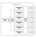
図1に示されているように、WLANデバイス1は、アンテナ11、無線周波数チップ(無線周波数集積回路、radio frequency integrated circuit、すなわちRFICとも呼ばれる)12、およびベースバンド(base band、BB)チップ13などのコンポーネントを含む。無線周波数チップはベースバンドチップとアンテナの両方に接続される。本出願の本実施形態において、ベースバンドチップは、ベースバンド処理回路と中間周波数処理回路とを含む。ベースバンド処理回路は、ベースバンド回路、媒体アクセス制御(media access control、MAC)回路、および物理層(physical layer、PHY)回路などを含む。中間周波数処理回路は、アナログフロントエンド(analog front end、AFE)回路とデジタルフロントエンド(digital front end、DFE)回路などを含む。アナログフロントエンド回路は、アナログ信号を処理するように構成される。デジタルフロントエンド回路は、デジタル信号を処理するように構成される。したがって、本出願の本実施形態におけるベースバンドチップはシステム・オン・チップ(system on chip、SOC)とも呼ばれ、中間周波数処理回路はデジタル中間周波数回路とも呼ばれる。加えて、ベースバンドチップは集積回路(integrated circuit、IC)であってよい。無線周波数チップは無線周波数集積回路(radio frequency integrated circuit、RFIC)と呼ばれることもある。
As shown in FIG. 1, the WLAN device 1 includes an antenna 11, a radio frequency integrated circuit (also called an RFIC) 12, and a base band (BB)
WLANデバイスは信号を送受できる。WLANデバイスが信号を受信する過程では、WLANデバイス内のコンポーネントが次のように協働する。アンテナは電波を受信し、電波を無線周波数信号に変換し、変換によって得られた無線周波数信号を無線周波数チップへ送信する。無線周波数チップは無線周波数信号を中間周波数信号に変換し、変換によって得られた中間周波数信号に対して信号処理を行い、処理された中間周波数信号をベースバンドチップへ送信する。ベースバンドチップは中間周波数信号に基づいてデータ信号を得、得られたデータ信号を出力する。データ信号は、WLANデバイスによって受信される信号に対して行われる必要のある実際の作業を指示し、例えば、ウェブサイトにアクセスするため端末によって送信されるアクセス要求のために行われるべき作業を指示する。 WLAN devices can send and receive signals. As the WLAN device receives the signal, the components within the WLAN device work together as follows: The antenna receives the radio wave, converts the radio wave into a radio frequency signal, and transmits the radio frequency signal obtained by the conversion to the radio frequency chip. The radio frequency chip converts the radio frequency signal into an intermediate frequency signal, performs signal processing on the intermediate frequency signal obtained by the conversion, and transmits the processed intermediate frequency signal to the baseband chip. The baseband chip obtains a data signal based on the intermediate frequency signal and outputs the obtained data signal. The data signal dictates the actual work that needs to be done on the signal received by the WLAN device, for example, the work that should be done for the access request sent by the terminal to access the website. do.
WLANデバイスが信号を送信する過程では、WLANデバイス内のコンポーネントが次のように協働する。ベースバンドチップは受信されたデータ信号に基づいて中間周波数信号を生成し、得られた中間周波数信号に対して信号処理を行い、処理された中間周波数信号を無線周波数チップへ送信する。無線周波数チップは中間周波数信号に対して信号処理を行い、処理された中間周波数信号を無線周波数信号に変換し、変換によって得られた無線周波数信号をアンテナへ送信する。アンテナは無線周波数信号を電波に変換し、電波を伝送する。 As the WLAN device sends the signal, the components in the WLAN device work together as follows: The baseband chip generates an intermediate frequency signal based on the received data signal, performs signal processing on the obtained intermediate frequency signal, and transmits the processed intermediate frequency signal to the radio frequency chip. The radio frequency chip performs signal processing on the intermediate frequency signal, converts the processed intermediate frequency signal into a radio frequency signal, and transmits the radio frequency signal obtained by the conversion to the antenna. The antenna converts the radio frequency signal into radio waves and transmits the radio waves.
WLAN技術では、周波数帯域が1つの2.4 GHz周波数帯域から5 GHz周波数帯域に拡大される。加えて、多重入出力(multi-input multi-output、MIMO)技術も成熟し、初期の2アンテナ技術から4アンテナ技術または8アンテナ技術に進化する。したがって、複数のマルチバンドアンテナでWLANデバイスが構成されることは必然のトレンドである。しかし、MIMO技術では、複数のアンテナが同じ周波数帯域に属する信号を同時に送信し受信する必要があり、WLANデバイス内の別々のアンテナは互いに完全には単離されていないため、WLANデバイスのいずれかのアンテナによって伝送される信号は、空間的結合によってWLANデバイスの別のアンテナに漏れる。しかし、WLANデバイス内のアンテナで伝送される信号は異なる。したがって、別のアンテナに漏れる信号は別のアンテナの干渉信号になる。 With WLAN technology, the frequency band is expanded from one 2.4 GHz frequency band to the 5 GHz frequency band. In addition, multi-input multi-output (MIMO) technology has matured and evolved from the early two-antenna technology to four-antenna or eight-antenna technology. Therefore, it is an inevitable trend to configure a WLAN device with multiple multi-band antennas. However, MIMO technology requires multiple antennas to simultaneously transmit and receive signals belonging to the same frequency band, and the separate antennas within a WLAN device are not completely isolated from each other, so any of the WLAN devices. The signal transmitted by one of the antennas leaks to another antenna of the WLAN device due to spatial coupling. However, the signals transmitted by the antenna in the WLAN device are different. Therefore, the signal leaking to another antenna becomes the interference signal of another antenna.
一実装においては、アンテナ間の干渉信号の信号強度を軽減するため、WLANデバイス上のアンテナ間の間隔はできるだけ大きく設定できる。加えて、アンテナ間の間隔をできるだけ大きく設定するため、WLANデバイス内のアンテナは通常ならばマルチバンドアンテナである。WLANデバイスが複数の周波数帯域をサポートするときに、それぞれの無線周波数チップがただ1つの周波数帯域をサポートする場合は、WLANデバイス内に複数の無線周波数チップが存在し、複数の無線周波数チップのうちの少なくとも2つの無線周波数チップに同一のアンテナを接続する必要があり、WLANデバイス上で同じ動作周波数帯域を有する全てのアンテナを同一の無線周波数チップに接続する必要がある。この接続方法では、無線周波数チップといずれかのアンテナとの間の無線周波数トレースは比較的長く、無線周波数トレース上で比較的大きい信号損失が生じる。加えて、無線周波数チップと各アンテナとの間で無線周波数トレースの交差を回避するためにいくつかの措置が講じられ、これらの措置によって無線周波数トレース上の信号損失はさらに増大し、WLANデバイスの性能に悪影響を及ぼす。 In one implementation, the spacing between the antennas on the WLAN device can be set as large as possible in order to reduce the signal strength of the interference signal between the antennas. In addition, the antennas in the WLAN device are usually multi-band antennas in order to set the spacing between the antennas as large as possible. If a WLAN device supports multiple frequency bands and each radio frequency chip supports only one frequency band, then there are multiple radio frequency chips within the WLAN device and of the multiple radio frequency chips. It is necessary to connect the same antenna to at least two radio frequency chips of, and all antennas with the same operating frequency band on the WLAN device need to be connected to the same radio frequency chip. With this connection method, the radio frequency trace between the radio frequency chip and either antenna is relatively long, resulting in a relatively large signal loss on the radio frequency trace. In addition, some measures have been taken to avoid crossing the radio frequency trace between the radio frequency chip and each antenna, which will further increase the signal loss on the radio frequency trace and of the WLAN device. It adversely affects performance.
本出願の一実施形態は無線周波数チップを提供する。無線周波数チップは少なくとも2つの周波数帯域をサポートできる。換言すると、無線周波数チップは少なくとも2つの周波数帯域の無線周波数信号を送受できる。WLANデバイス内の無線周波数チップが本出願の本実施形態で提供される無線周波数チップである場合は、無線周波数チップが少なくとも2つの周波数帯域の無線周波数信号を送受できるため、少なくとも2つの周波数帯域の無線周波数信号を送受するように構成されたアンテナに無線周波数チップを接続できる。このように、少なくとも2つの周波数帯域の無線周波数信号を送受するように構成されたアンテナが、ただ1つの周波数帯域をサポートする少なくとも2つの無線周波数チップに別々に接続される必要はない。したがって、WLANデバイスでアンテナと無線周波数チップとの間の無線周波数トレースを配置する際は、アンテナと無線周波数チップの配備位置に基づいて、無線周波数トレースを柔軟に配置できる。これは、無線周波数チップとアンテナとの間の無線周波数トレースの長さを縮め、無線周波数トレースが交差する可能性を抑え、無線周波数トレース上での信号損失を減らし、したがって、無線周波数チップが配置されたWLANデバイスの性能を高めるのに役立つ。 One embodiment of the present application provides a radio frequency chip. The radio frequency chip can support at least two frequency bands. In other words, the radio frequency chip can send and receive radio frequency signals in at least two frequency bands. When the radio frequency chip in the WLAN device is the radio frequency chip provided in the present embodiment of the present application, the radio frequency chip can send and receive radio frequency signals in at least two frequency bands, so that the radio frequency chip has at least two frequency bands. A radio frequency chip can be connected to an antenna configured to send and receive radio frequency signals. Thus, antennas configured to send and receive radio frequency signals in at least two frequency bands need not be separately connected to at least two radio frequency chips that support only one frequency band. Therefore, when arranging the radio frequency trace between the antenna and the radio frequency chip in the WLAN device, the radio frequency trace can be flexibly arranged based on the deployment position of the antenna and the radio frequency chip. This shortens the length of the radio frequency trace between the radio frequency chip and the antenna, reduces the possibility of crossing radio frequency traces, reduces signal loss on the radio frequency trace, and therefore the radio frequency chip is placed. Helps improve the performance of wireless devices.
図2は、本出願の一実施形態による無線周波数チップ12の概略構造図である。図2に示されているように、無線周波数チップ12は、少なくとも2つの信号生成回路121、少なくとも3つの無線周波数トランシーバ回路122、および少なくとも3つの中間周波数トランシーバ回路123などのコンポーネントを含む。少なくとも2つの信号生成回路121は、第1の信号生成回路121と第2の信号生成回路121とを含む。少なくとも3つの無線周波数トランシーバ回路122は、少なくとも3つの中間周波数トランシーバ回路123に1対1に対応する形で接続される。加えて、それぞれの無線周波数トランシーバ回路122は、WLANデバイス1内のアンテナ11に接続するようにさらに構成され、それぞれの中間周波数トランシーバ回路123は、WLANデバイス1内のベースバンドチップ13に接続するようにさらに構成される。図2は、2つの信号生成回路121と、3つの無線周波数トランシーバ回路122と、3つの中間周波数トランシーバ回路123とを含む無線周波数チップ12の概略構造図である。無線周波数チップ12内のコンポーネントの働きは次の通りである。
FIG. 2 is a schematic structural diagram of a
第1の信号生成回路121は、第1の無線周波数局部発振器信号を生成するように構成される。第2の信号生成回路121は、第2の無線周波数局部発振器信号を生成するように構成される。第1の無線周波数局部発振器信号が属する周波数帯域は、第2の無線周波数局部発振器信号が属する周波数帯域と異なる。例えば、第1の無線周波数局部発振器信号と第2の無線周波数局部発振器信号のいずれか一方は2.4 GHz周波数帯域に属し、他方は5 GHz周波数帯域に属する。別の一例として、第1の無線周波数局部発振器信号と第2の無線周波数局部発振器信号のいずれか一方は5 GHz周波数帯域の低帯域(low band)に属し、他方は5 GHz周波数帯域の高帯域(high band)に属する。
The first
第1の信号生成回路121は、少なくとも3つの無線周波数トランシーバ回路122のうちの少なくとも1つの無線周波数トランシーバ回路122のために第1の無線周波数局部発振器信号を提供するように構成される。第2の信号生成回路121は、少なくとも3つの無線周波数トランシーバ回路122のうちの少なくとも1つの無線周波数トランシーバ回路122のために第2の無線周波数局部発振器信号を提供するように構成される。少なくとも3つの無線周波数トランシーバ回路122のうちのいずれかの無線周波数トランシーバ回路122は、一度に少なくとも2つの信号生成回路121のうちのいずれか1つからの無線周波数局部発振器信号のみ受信する。
The first
少なくとも3つの無線周波数トランシーバ回路122の各々は、受信された無線周波数局部発振器信号に基づいて受信された無線周波数信号を中間周波数信号に変換し、得られた中間周波数信号を対応する中間周波数トランシーバ回路123へ送信するように、または対応する中間周波数トランシーバ回路123からの中間周波数信号を無線周波数信号に変換し、得られた無線周波数信号を出力するように、構成される。例えば、信号送信プロセスでは、無線周波数チップ12の中間周波数信号ピンから中間周波数信号を受信した後に、中間周波数トランシーバ回路123が中間周波数信号に対して信号処理を行い、処理された中間周波数信号を対応する無線周波数トランシーバ回路122へ送信することができる。その後、無線周波数トランシーバ回路122は無線周波数局部発振器信号に基づいて中間周波数信号を無線周波数信号に変換し、変換によって得られた無線周波数信号を無線周波数チップ12の無線周波数信号ピンを使用して出力する。信号受信プロセスでは、無線周波数信号ピンから無線周波数信号を受信した後に、無線周波数トランシーバ回路122が無線周波数局部発振器信号に基づいて無線周波数信号を中間周波数信号に変換し、変換によって得られた中間周波数信号を対応する中間周波数トランシーバ回路123へ送信することができる。その後、中間周波数トランシーバ回路123は中間周波数信号に対して信号処理を行い、変換によって得られた中間周波数信号を中間周波数信号ピンを使用して出力する。無線周波数信号ピンは、無線周波数チップ12と、無線周波数信号ピンを使用して無線周波数チップ12に接続された別のデバイスとの間で、無線周波数信号を伝送するように構成される。中間周波数信号ピンは、無線周波数チップ12と、中間周波数信号ピンを使用して無線周波数チップ12に接続された別のデバイスとの間で、中間周波数信号を伝送するように構成される。
Each of the at least three radio frequency transceiver circuits 122 converts the received radio frequency signal to an intermediate frequency signal based on the received radio frequency local oscillator signal, and the obtained intermediate frequency signal is the corresponding intermediate frequency transceiver circuit. It is configured to transmit to 123 or to convert the intermediate frequency signal from the corresponding intermediate frequency transceiver circuit 123 into a radio frequency signal and output the resulting radio frequency signal. For example, in the signal transmission process, after receiving an intermediate frequency signal from the intermediate frequency signal pin of the
少なくとも3つの無線周波数トランシーバ回路122のうちの2つの無線周波数トランシーバ回路122は、受信された中間周波数信号を無線周波数信号に変換でき、あるいは第1の無線周波数局部発振器信号と第2の無線周波数局部発振器信号とにそれぞれ基づいて受信された無線周波数信号を中間周波数信号に変換でき、第1の無線周波数局部発振器信号が属する周波数帯域は第2の無線周波数局部発振器信号が属する周波数帯域と異なる。したがって、無線周波数チップ12は少なくとも2つの周波数帯域をサポートでき、すなわち、無線周波数チップは少なくとも2つの周波数帯域の無線周波数信号を送受できる。WLANデバイス内の無線周波数チップが本出願の本実施形態で提供される無線周波数チップである場合は、無線周波数チップが少なくとも2つの周波数帯域の無線周波数信号を送受できるため、少なくとも2つの周波数帯域の無線周波数信号を送受するように構成されたアンテナに無線周波数チップを接続できる。このように、少なくとも2つの周波数帯域の無線周波数信号を送受するように構成されたアンテナが、ただ1つの周波数帯域をサポートする少なくとも2つの無線周波数チップに別々に接続される必要はない。したがって、WLANデバイスでアンテナと無線周波数チップとの間の無線周波数トレースを配置する際は、アンテナ11と無線周波数チップ12の配備位置に基づいて、無線周波数トレースを柔軟に配置できる。これは無線周波数チップ12とアンテナ11との間の無線周波数トレースの長さを縮め、無線周波数トレースが交差する可能性を抑えるのに役立つ。
Two of the at least three radio frequency transceiver circuits 122 can convert the received intermediate frequency signal into a radio frequency signal, or the first radio frequency local oscillator signal and the second radio frequency local. The radio frequency signal received based on the oscillator signal can be converted into an intermediate frequency signal, and the frequency band to which the first radio frequency local oscillator signal belongs is different from the frequency band to which the second radio frequency local oscillator signal belongs. Therefore, the
例えば、図9、図10、図12、および図13を参照し、無線周波数チップ122aが2つの周波数帯域をサポートし、アンテナ111が2つの周波数帯域をサポートするデュアルバンドアンテナである場合、アンテナ111は無線周波数チップ122aのみに接続されればよく、別々の周波数帯域をサポートする2つの無線周波数チップに別々に接続する必要はない。別の一例として、図9、図10、図12、および図13を引き続き参照し、無線周波数チップ122aが2つの周波数帯域をサポートし、アンテナ111とアンテナ112が2つの周波数帯域でそれぞれ動作する場合、アンテナ111とアンテナ112はいずれも無線周波数チップ122aに接続できる。換言すると、アンテナ111とアンテナ112はいずれも、動作周波数帯域が2つの周波数帯域である2つの無線周波数チップに1対1に対応する形で接続される必要はない。したがって、WLANデバイス内の無線周波数チップが本出願の本実施形態で提供される無線周波数チップである場合は、無線周波数トレースを配置する方法を最適化でき、無線周波数トレースの長さを縮めることができ、無線周波数トレースが交差する可能性を抑えることができる。
For example, see FIGS. 9, 10, 12, and 13 if the
無線周波数トランシーバ回路122(TRX)は、内部低雑音増幅器(internal low-noise amplifier、iLNA)、ミキサー(Mixer)、トランスインピーダンス増幅器(trans-impedance amplifier、TIA)、アップリンクパワーコントロール(uplink power control、UPC)、およびパルスパワー増幅器(pulsed power amplifier、PPA)などの無線周波数回路を含む。中間周波数トランシーバ回路123は、可変利得増幅器(variable gain amplifier、VGA)、ローパスフィルタ(low pass filter、LPF)、および送信バッファ(transmit buffer)などのアナログベースバンド回路を含む。無線周波数トランシーバ回路122が受信された無線周波数局部発振器信号に基づいて受信された無線周波数信号を中間周波数信号に変換するプロセスは、受信された無線周波数信号に対するダウンコンバージョンと呼ばれることがある。無線周波数トランシーバ回路122が対応する中間周波数トランシーバ回路123からの中間周波数信号を無線周波数信号に変換するプロセスは、受信された中間周波数信号に対するアップコンバージョンと呼ばれることがある。 The radio frequency transceiver circuit 122 (TRX) is an internal low-noise amplifier (iLNA), mixer (Mixer), trans-impedance amplifier (TIA), uplink power control, Includes UPC), and radio frequency circuits such as pulsed power amplifiers (PPAs). The intermediate frequency transceiver circuit 123 includes analog baseband circuits such as a variable gain amplifier (VGA), a low pass filter (LPF), and a transmit buffer. The process by which the radio frequency transceiver circuit 122 converts a received radio frequency signal to an intermediate frequency signal based on the received radio frequency local oscillator signal is sometimes referred to as down conversion to the received radio frequency signal. The process by which the radio frequency transceiver circuit 122 converts the intermediate frequency signal from the corresponding intermediate frequency transceiver circuit 123 into a radio frequency signal is sometimes referred to as upconversion to the received intermediate frequency signal.
一実装において、信号生成回路121は位相ロックループ(phase lock loop、PLL)であってよい。
In one implementation, the
加えて、少なくとも2つの信号生成回路121のうちの信号生成回路121は、互いに影響を与えない。具体的に述べると、少なくとも2つの信号生成回路121によって生成される無線周波数局部発振器信号の周波数は互いにまったく異なってよく、あるいは、第1の信号生成回路121によって生成される第1の無線周波数局部発振器信号が属する周波数帯域が、第2の信号生成回路121によって生成される第2の無線周波数局部発振器信号が属する周波数帯域と異なることが最低でも保証されるのであるならば、一部の周波数は同じであり、他の周波数は異なる。これは本出願の本実施形態で具体的に限定されない。少なくとも2つの信号生成回路121によって生成される無線周波数局部発振器信号の周波数帯域が完全に異なる場合は、すなわち、少なくとも2つの信号生成回路のうちのいずれか2つの信号生成回路が別々の周波数帯域で動作する場合は、別々の信号生成回路121を使用して別々の周波数帯域の無線周波数局部発振器信号を生成することができる。したがって、それぞれの信号生成回路121を効果的に使用でき、無線周波数チップ12のコストを削減でき、無線周波数チップ12のサイズを縮小できる。
In addition, the
任意に選べることとして、無線周波数チップ12は少なくとも3つの無線周波数信号ピンを有し、本出願の本実施形態において、無線周波数信号ピンによって出力される信号が属する周波数帯域は、実際の要件に基づいて調整できる。このように、無線周波数信号ピンによって出力される無線周波数信号の周波数は様々な応用シナリオの要件に基づいて調整できるため、無線周波数チップ12は様々な応用シナリオに応用できる。
Optionally, the
無線周波数信号ピンによって出力される信号が属する周波数帯域を調整する一実装においては、無線周波数トランシーバ回路122の動作周波数帯域が調整されるため、無線周波数信号ピンによって出力される信号が属する周波数帯域は調整される。 Adjusting the frequency band to which the signal output by the radio frequency signal pin belongs In one implementation, the operating frequency band of the radio frequency transceiver circuit 122 is adjusted, so that the frequency band to which the signal output by the radio frequency signal pin belongs is It will be adjusted.
無線周波数チップ12は第1の制御回路(図3に図示せず)をさらに含む。第1の制御回路は、少なくとも2つの信号生成回路121が少なくとも3つの無線周波数トランシーバ回路122のために無線周波数局部発振器信号を提供するモードを制御するように構成される。換言すると、第1の制御回路は、生成された無線周波数局部発振器信号を特定の無線周波数トランシーバ回路122に提供する形にそれぞれの信号生成回路121を制御するように構成される。図3に示されているように、無線周波数チップ12の少なくとも3つの無線周波数信号ピンRは、少なくとも3つの無線周波数トランシーバ回路122に1対1に対応する形で接続される。このように、無線周波数信号ピンRによって出力される信号が属する周波数帯域は、無線周波数トランシーバ回路122の動作周波数帯域と同じである。無線周波数トランシーバ回路122によって受信される無線周波数局部発振器信号の周波数帯域が異なる場合は、無線周波数トランシーバ回路122の動作周波数帯域は異なり、無線周波数信号ピンRによって出力される信号が属する周波数帯域は相応に変わる。
The
一実装においては、図3に示されているように、少なくとも2つの信号生成回路121の各々と少なくとも3つの無線周波数トランシーバ回路122の各々との間に第1のスイッチ回路S11が配置される。この場合、第1の制御回路は、具体的には、少なくとも2つの信号生成回路121の各々によって出力される無線周波数局部発振器信号の行き先を変えるため、第1のスイッチ回路S11の動作状態を制御するように構成される。
In one implementation, as shown in FIG. 3, a first switch circuit S11 is placed between each of at least two
任意に選べることとして、第1の制御回路は、第1のスイッチ回路S11のために制御信号を提供することで、この制御信号を使用して第1のスイッチ回路S11内のスイッチをオンまたはオフになるように制御することができる。例えば、第1のスイッチ回路S11がトランジスタ回路である場合、第1の制御回路はこのトランジスタ回路の駆動回路であってよい。第1の制御回路は、第1のスイッチ回路S11を動作するように駆動するための制御信号を第1のスイッチ回路S11に提供でき、これにより第1のスイッチ回路S11内のスイッチのオン/オフ状態が制御される。 Optionally, the first control circuit provides a control signal for the first switch circuit S11 and uses this control signal to turn the switch in the first switch circuit S11 on or off. Can be controlled to be. For example, when the first switch circuit S11 is a transistor circuit, the first control circuit may be a drive circuit of this transistor circuit. The first control circuit can provide the first switch circuit S11 with a control signal for driving the first switch circuit S11 to operate, thereby turning on / off the switch in the first switch circuit S11. The state is controlled.
第1の制御回路は無線周波数チップ12の外に配置されてもよく、第1の制御回路が無線周波数チップ12上に配置されることが本出願で限定されないことに注意されたい。例えば、第1の制御回路はWLANデバイス上に配置されてもよい。
Note that the first control circuit may be located outside the
任意に選べることとして、第1のスイッチ回路S11の具体的な形態は実際の要件に基づいて設定できる。例えば、スイッチ回路は信号生成回路121と無線周波数トランシーバ回路122との間に配置されてよく、信号生成回路121と無線周波数トランシーバ回路122との間で導通状態を制御するように構成される。この場合、第1のスイッチ回路S11は、少なくとも2つの信号生成回路121と少なくとも3つの無線周波数トランシーバ回路122との間の全てのスイッチ回路を含む。一実装においては、図4に示されているように、信号生成回路121と無線周波数トランシーバ回路122との間に単極単投スイッチS111が配置されてよい。単極単投スイッチS111の静止接点と可動接点のいずれか一方は信号生成回路121に接続され、単極単投スイッチS111の静止接点と可動接点の他方は無線周波数トランシーバ回路122に接続される。図4では、各単極単投スイッチS111の可動接点が信号生成回路121に接続され、各単極単投スイッチS111の静止接点が無線周波数トランシーバ回路122に接続されている。この場合、図4の第1のスイッチ回路S11は、少なくとも2つの信号生成回路121と少なくとも3つの無線周波数トランシーバ回路との間に6つの単極単投スイッチS111を含んでいる。
As an arbitrary choice, the specific form of the first switch circuit S11 can be set based on actual requirements. For example, the switch circuit may be arranged between the
あるいは、スイッチ回路は信号生成回路121と全ての無線周波数トランシーバ回路122との間に配置されてもよく、信号生成回路121と全ての無線周波数トランシーバ回路122との間で導通状態を制御するように構成される。換言すると、無線周波数チップにおいて、少なくとも2つの信号生成回路121は、少なくとも2つの信号生成回路121と1対1の対応関係にある少なくとも2つのスイッチ回路を使用して少なくとも3つの無線周波数トランシーバ回路122に接続される。この場合、第1のスイッチ回路S11は少なくとも2つのスイッチ回路を含む。一実装においては、図5に示されているように、信号生成回路121と全ての無線周波数トランシーバ回路122との間に単極多投スイッチS112が配置されてよい。単極多投スイッチS112の静止接点は信号生成回路121に接続され、単極多投スイッチS112の各可動接点は1つの無線周波数トランシーバ回路122に接続され、単極多投スイッチS112の1つの静止接点は一度に1つ以上の可動接点に接続されてよい。この場合、図5の第1のスイッチ回路S11は、2つの信号生成回路121と1対1の対応関係にある2つの単極多投スイッチS112を含んでいる。図5は、2つの単極多投スイッチS112のうちの一方の単極多投スイッチS112の1つの静止接点が1つの可動接点に接続され、2つの単極多投スイッチS112のうちの他方の単極多投スイッチS112の1つの静止接点が2つの可動接点に接続されている概略図である。
Alternatively, the switch circuit may be located between the
あるいは、スイッチ回路は1つの無線周波数トランシーバ回路122と全ての信号生成回路121との間に配置されてもよく、無線周波数トランシーバ回路122と全ての信号生成回路121の導通状態を制御するように構成される。換言すると、無線周波数チップ12内の少なくとも3つの無線周波数トランシーバ回路122は、少なくとも3つの無線周波数トランシーバ回路122と1対1の対応関係にある少なくとも3つのスイッチ回路を使用して少なくとも2つの信号生成回路121に接続される。この場合、第1のスイッチ回路S11は少なくとも3つのスイッチ回路を含む。一実装においては、無線周波数トランシーバ回路122と全ての信号生成回路121との間に単極多投スイッチが配置されてよい。この単極多投スイッチの静止接点は無線周波数トランシーバ回路122に接続され、単極多投スイッチの各可動接点は1つの信号生成回路121に接続され、単極多投スイッチの1つの静止接点は一度にただ1つの可動接点に接続される。この場合、第1のスイッチ回路S11は少なくとも3つの単極多投スイッチを含む。
Alternatively, the switch circuit may be located between one radio frequency transceiver circuit 122 and all
あるいは、第1のスイッチ回路S11は、複数の第1の末端と複数の第2の末端とを有するスイッチ回路であってよい。複数の第1の末端は全ての無線周波数トランシーバ回路122に1対1に対応する形で接続され、複数の第2の末端は全ての信号生成回路121に1対1に対応する形で接続される。このスイッチ回路は、第1の末端と第2の末端との間で導通状態を個別に制御できる。
Alternatively, the first switch circuit S11 may be a switch circuit having a plurality of first ends and a plurality of second ends. The plurality of first ends are connected to all radio frequency transceiver circuits 122 in a one-to-one correspondence, and the plurality of second ends are connected to all
前述した第1のスイッチ回路S11の数通りの実装において、2つの別々の回路が共通の部分を持たない2つの回路であってよいこと、あるいは様々な分割原理による分割で得られる回路であってよいことに注意されたい。加えて、前述した第1のスイッチ回路S11の数通りの実装は第1のスイッチ回路S11の実装例に過ぎず、第1のスイッチ回路S11の具体的な実装を制限するために使用されない。当業者なら、本出願の本実施形態で提供される無線周波数チップを実装する際に、実際の要件に基づいて第1のスイッチ回路S11の具体的な実装を調整できる。これは本出願の本実施形態で具体的に限定されない。 In several implementations of the first switch circuit S11 described above, two separate circuits may be two circuits having no common part, or a circuit obtained by division according to various division principles. Please note that it is good. In addition, the several implementations of the first switch circuit S11 described above are merely implementation examples of the first switch circuit S11 and are not used to limit the specific implementation of the first switch circuit S11. One of ordinary skill in the art can adjust the specific implementation of the first switch circuit S11 based on actual requirements when mounting the radio frequency chip provided in this embodiment of the present application. This is not specifically limited in this embodiment of the present application.
加えて、第1のスイッチ回路S11はアナログスイッチ回路であってよく、例えば、切り替え機能を有し、電界効果トランジスタを使用して実装される回路であってよい。あるいは、第1のスイッチ回路S11はデジタルスイッチ回路であってもよく、例えば、切り替え機能を有し、ゲート回路を使用して実装される回路であってもよい。あるいは、第1のスイッチ回路S11は、切り替え機能を有し、特定用途向け集積回路(application-specific integrated circuit、ASIC)またはプログラマブルロジックデバイス(programmable logic device、PLD)を使用して実装される回路であってもよい。これは本出願の本実施形態で具体的に限定されない。PLDは、複合プログラマブルロジックデバイス(complex programmable logic device、CPLD)、フィールドプログラマブルゲートアレイ(field-programmable gate array、FPGA)、ジェネリックアレイロジック(generic array logic、GAL)、またはこれらの任意の組み合わせであってよい。 In addition, the first switch circuit S11 may be an analog switch circuit, for example, a circuit having a switching function and mounted using a field effect transistor. Alternatively, the first switch circuit S11 may be a digital switch circuit, for example, a circuit having a switching function and mounted using a gate circuit. Alternatively, the first switch circuit S11 is a circuit that has a switching function and is implemented using an application-specific integrated circuit (ASIC) or a programmable logic device (PLD). There may be. This is not specifically limited in this embodiment of the present application. A PLD can be a complex programmable logic device (CPLD), a field-programmable gate array (FPGA), a generic array logic (GAL), or any combination thereof. good.
別の可能な一実装において、少なくとも2つの信号生成回路121はいずれもマルチチャネル出力回路であってよく、3つの無線周波数トランシーバ回路122の各々は少なくとも2つの信号生成回路121の各々の出力ポートに接続される。この場合、第1の制御回路は、具体的には、少なくとも2つの信号生成回路121の各々によって出力される無線周波数局部発振器信号の行き先を変えるため、少なくとも2つの信号生成回路121の各々の出力ポートの出力状態を制御するように構成される。
In another possible implementation, at least two
例えば、無線周波数チップ12が2つの信号生成回路121と4つの無線周波数トランシーバ回路122を含むと仮定する。2つの信号生成回路121はそれぞれ第1の信号生成回路121と第2の信号生成回路121である。第1の信号生成回路121と第2の信号生成回路121は4つの出力ポートを各々有し、4つの無線周波数トランシーバ回路122は第1の信号生成回路121の4つの出力ポートに1対1に対応する形で接続され、4つの無線周波数トランシーバ回路122は第2の信号生成回路121の4つの出力ポートに1対1に対応する形で接続される。第1の制御回路は、第1の信号生成回路121が、4つの出力ポートのいずれか1つを使用して、第1の信号生成回路121によって生成される第1の無線周波数局部発振器信号を、4つの出力ポートのいずれか1つに接続された信号生成回路121へ出力するか否かを制御するため、第1の信号生成回路121の各出力ポートの出力状態を制御できる。同様に、第1の制御回路はまた、第2の信号生成回路121によって生成される第2の無線周波数局部発振器信号の出力先を制御するため、この方法で、第2の信号生成回路121の出力ポートの出力状態を制御できる。
For example, suppose the
無線周波数信号ピンによって出力される信号が属する周波数帯域を調整する別の一実装においては、無線周波数チップ12の少なくとも3つの無線周波数信号ピンの各々が少なくとも2つの無線周波数トランシーバ回路122の各々に接続される。このように、無線周波数チップ12の複数の無線周波数トランシーバ回路122が無線周波数信号ピンに信号を提供するモードは調整でき、すなわち、無線周波数信号ピンによって出力される信号が属する周波数帯域の調整を実施するため、無線周波数トランシーバ回路122と無線周波数信号ピンとの接続方法は調整できる。
In another implementation that adjusts the frequency band to which the signal output by the radio frequency signal pin belongs, each of the at least three radio frequency signal pins of the
無線周波数チップ12は第3の制御回路(図6に図示せず)をさらに含む。第3の制御回路は、無線周波数チップ12内の複数の無線周波数トランシーバ回路122と無線周波数信号ピンの接続状態を制御するように構成される。具体的に述べると、第3の制御回路は、特定の無線周波数信号ピンに接続する形にそれぞれの無線周波数トランシーバ回路122を制御するように構成され、無線周波数信号ピンによって出力される信号が属する周波数帯域は、無線周波数信号ピンに接続された無線周波数トランシーバ回路122の動作周波数帯域と同じになる。
The
一実装においては、図6に示されているように、少なくとも3つの無線周波数トランシーバ回路122の各々は、第2のスイッチ回路S12を使用して少なくとも3つの無線周波数信号ピンRの各々に接続されてよい。無線周波数チップ12が動作するときに、少なくとも3つの無線周波数トランシーバ回路122は少なくとも3つの無線周波数信号ピンRに1対1に対応する形で接続される。この場合、第3の制御回路は、具体的には、無線周波数トランシーバ回路122と無線周波数信号ピンRとの接続方法を変えるため、第2のスイッチ回路S12の動作状態を制御するように構成される。様々な応用シナリオでは、無線周波数信号ピンRと無線周波数トランシーバ回路122との導通状態を調整するため、第3の制御回路は応用要件に基づいて第2のスイッチ回路S12の動作状態を調整できる。
In one implementation, each of at least three radio frequency transceiver circuits 122 is connected to each of at least three radio frequency signal pins R using a second switch circuit S12, as shown in FIG. It's okay. When the
任意に選べることとして、第3の制御回路は第2のスイッチ回路S12のために制御信号を提供することで、この制御信号を使用して第2のスイッチ回路S12内のスイッチをオンまたはオフになるように制御することができる。例えば、第2のスイッチ回路S12がトランジスタ回路である場合、第3の制御回路はこのトランジスタ回路の駆動回路であってよく、第3の制御回路は、第2のスイッチ回路S12を動作するように駆動するための制御信号を第2のスイッチ回路S12に提供でき、これにより第2のスイッチ回路S12内のスイッチのオン/オフ状態が制御される。 Optionally, the third control circuit provides a control signal for the second switch circuit S12 and uses this control signal to turn the switch in the second switch circuit S12 on or off. Can be controlled to be. For example, if the second switch circuit S12 is a transistor circuit, the third control circuit may be the drive circuit of this transistor circuit, and the third control circuit may operate the second switch circuit S12. A control signal for driving can be provided to the second switch circuit S12, which controls the on / off state of the switch in the second switch circuit S12.
第3の制御回路は無線周波数チップ12の外に配置されてもよく、第1の制御回路が無線周波数チップ12上に配置されることが本出願で限定されないことに注意されたい。例えば、第3の制御回路はWLANデバイス上に配置されてもよい。加えて、第1の制御回路と第3の制御回路は同一回路の別々の部分であってよく、あるいは互いに独立した2つの回路であってもよい。第1の制御回路と第3の制御回路の具体的な配備モードは、本出願の本実施形態で限定されない。
Note that the third control circuit may be located outside the
任意に選べることとして、第2のスイッチ回路S12の具体的な形態は実際の要件に基づいて設定できる。例えば、スイッチ回路は無線周波数信号ピンRと無線周波数トランシーバ回路122との間に配置されてよく、無線周波数信号ピンRと無線周波数トランシーバ回路122との間で導通状態を制御するように構成される。この場合、第2のスイッチ回路S12は、少なくとも3つの無線周波数信号ピンRと少なくとも3つの無線周波数トランシーバ回路122との間の全てのスイッチ回路を含む。一実装においては、図7に示されているように、無線周波数信号ピンRと無線周波数トランシーバ回路122との間に単極単投スイッチS121が配置されてよい。単極単投スイッチS121の静止接点と可動接点のいずれか一方は無線周波数信号ピンRに接続され、単極単投スイッチS121の静止接点と可動接点の他方は無線周波数トランシーバ回路122に接続される。図7では、各単極単投スイッチS121の静止接点が無線周波数信号ピンRに接続され、各単極単投スイッチS121の可動接点が無線周波数トランシーバ回路122に接続されている。この場合、図7の第2のスイッチ回路S12は、少なくとも3つの無線周波数信号ピンRと少なくとも3つの無線周波数トランシーバ回路122との間に9つの単極単投スイッチS121を含んでいる。 As an option, the specific form of the second switch circuit S12 can be set based on actual requirements. For example, the switch circuit may be located between the radio frequency signal pin R and the radio frequency transceiver circuit 122 and is configured to control the conduction state between the radio frequency signal pin R and the radio frequency transceiver circuit 122. .. In this case, the second switch circuit S12 includes all switch circuits between at least three radio frequency signal pins R and at least three radio frequency transceiver circuits 122. In one implementation, the unipolar single throw switch S121 may be located between the radio frequency signal pin R and the radio frequency transceiver circuit 122, as shown in FIG. One of the quiescent and movable contacts of the unipolar single throw switch S121 is connected to the radio frequency signal pin R, and the other of the quiescent and movable contacts of the unipolar single throw switch S121 is connected to the radio frequency transceiver circuit 122. .. In FIG. 7, the quiescent contact of each unipolar single throw switch S121 is connected to the radio frequency signal pin R, and the movable contact of each unipolar single throw switch S121 is connected to the radio frequency transceiver circuit 122. In this case, the second switch circuit S12 in FIG. 7 includes nine unipolar single throw switches S121 between at least three radio frequency signal pins R and at least three radio frequency transceiver circuits 122.
あるいは、スイッチ回路は無線周波数信号ピンRと全ての無線周波数トランシーバ回路122との間に配置されてもよく、無線周波数信号ピンRと全ての無線周波数トランシーバ回路122との間で導通状態を制御するように構成される。換言すると、無線周波数チップにおいて、少なくとも3つの無線周波数信号ピンRは、少なくとも3つの無線周波数信号ピンRと1対1の対応関係にある少なくとも3つのスイッチ回路を使用して少なくとも3つの無線周波数トランシーバ回路122に接続される。この場合、第2のスイッチ回路S12は少なくとも3つのスイッチ回路を含む。一実装においては、図8に示されているように、無線周波数信号ピンRと全ての無線周波数トランシーバ回路122との間に単極多投スイッチS122が配置されてよい。単極多投スイッチS122の静止接点は無線周波数信号ピンRに接続され、単極多投スイッチS122の各可動接点は1つの無線周波数トランシーバ回路122に接続され、単極多投スイッチS122の静止接点は一度にただ1つの可動接点に接続される。この場合、図8の第2のスイッチ回路S12は、少なくとも3つの単極多投スイッチS122を含んでいる。 Alternatively, the switch circuit may be located between the radio frequency signal pin R and all radio frequency transceiver circuits 122 to control the conduction state between the radio frequency signal pin R and all radio frequency transceiver circuits 122. It is configured as follows. In other words, in a radio frequency chip, at least three radio frequency signal pins R have at least three radio frequency transceivers using at least three switch circuits in a one-to-one correspondence with at least three radio frequency signal pins R. Connected to circuit 122. In this case, the second switch circuit S12 includes at least three switch circuits. In one implementation, as shown in FIG. 8, a unipolar multi-throw switch S122 may be placed between the radio frequency signal pin R and all radio frequency transceiver circuits 122. The quiescent contact of the unipolar multi-throw switch S122 is connected to the radio frequency signal pin R, each movable contact of the unipolar multi-throw switch S122 is connected to one radio frequency transceiver circuit 122, and the quiescent contact of the unipolar multi-throw switch S122. Is connected to only one movable contact at a time. In this case, the second switch circuit S12 in FIG. 8 includes at least three unipolar multi-throw switches S122.
あるいは、スイッチ回路は無線周波数トランシーバ回路122と全ての無線周波数信号ピンRとの間に配置されてもよく、無線周波数トランシーバ回路122と全ての無線周波数信号ピンRとの間で導通状態を制御するように構成される。換言すると、無線周波数チップ12において、少なくとも3つの無線周波数トランシーバ回路122は、少なくとも3つの無線周波数トランシーバ回路122と1対1の対応関係にある少なくとも3つのスイッチ回路を使用して少なくとも3つの無線周波数信号ピンRに接続される。この場合、第2のスイッチ回路S12は少なくとも3つのスイッチ回路を含む。一実装においては、無線周波数トランシーバ回路122と全ての無線周波数信号ピンRとの間に単極多投スイッチが配置されてよい。この単極多投スイッチの静止接点は無線周波数トランシーバ回路122に接続され、単極多投スイッチの各可動接点は1つの無線周波数信号ピンRに接続され、単極多投スイッチの静止接点は一度にただ1つの可動接点に接続される。この場合、第2のスイッチ回路S12は少なくとも3つの単極多投スイッチを含む。
Alternatively, the switch circuit may be located between the radio frequency transceiver circuit 122 and all radio frequency signal pins R to control the conduction state between the radio frequency transceiver circuit 122 and all radio frequency signal pins R. It is configured as follows. In other words, in the
あるいは、第2のスイッチ回路S12は、複数の第1の末端と複数の第2の末端とを有するスイッチ回路であってよい。複数の第1の末端は全ての無線周波数トランシーバ回路122に1対1に対応する形で接続され、複数の第2の末端は全ての無線周波数信号ピンRに1対1に対応する形で接続される。このスイッチ回路は、第1の末端と第2の末端との間で導通状態を個別に制御できる。 Alternatively, the second switch circuit S12 may be a switch circuit having a plurality of first ends and a plurality of second ends. The plurality of first ends are connected to all radio frequency transceiver circuits 122 in a one-to-one correspondence, and the plurality of second ends are connected to all radio frequency signal pins R in a one-to-one correspondence. Will be done. This switch circuit can individually control the conduction state between the first end and the second end.
前述した第2のスイッチ回路S12の数通りの実装において、2つの別々の回路が共通の部分を持たない2つの回路であってよいこと、あるいは様々な分割原理による分割で得られる回路であってよいことに注意されたい。加えて、前述した第2のスイッチ回路S12の数通りの実装は第2のスイッチ回路S12の実装例に過ぎず、第2のスイッチ回路S12の具体的な実装を制限するために使用されない。当業者なら、本出願の本実施形態で提供される無線周波数チップを実装する際に、実際の要件に基づいて第2のスイッチ回路S12の具体的な実装を調整できる。これは本出願の本実施形態で具体的に限定されない。 In several implementations of the second switch circuit S12 described above, two separate circuits may be two circuits that do not have a common part, or a circuit obtained by division according to various division principles. Please note that it is good. In addition, the several implementations of the second switch circuit S12 described above are merely implementation examples of the second switch circuit S12 and are not used to limit the specific implementation of the second switch circuit S12. One of ordinary skill in the art can adjust the specific implementation of the second switch circuit S12 based on actual requirements when implementing the radio frequency chip provided in this embodiment of the present application. This is not specifically limited in this embodiment of the present application.
加えて、第2のスイッチ回路S12はアナログスイッチ回路であってよく、例えば、切り替え機能を有し、電界効果トランジスタを使用して実装される回路であってよい。あるいは、第2のスイッチ回路S12はデジタルスイッチ回路であってもよく、例えば、切り替え機能を有し、ゲート回路を使用して実装される回路であってもよい。あるいは、第2のスイッチ回路S12は、切り替え機能を有し、特定用途向け集積回路またはプログラマブルロジックデバイスを使用して実装される回路であってもよい。これは本出願の本実施形態で具体的に限定されない。プログラマブルロジックデバイスは、複合プログラマブルロジックデバイス、フィールドプログラマブルゲートアレイ、ジェネリックアレイロジック、またはこれらの任意の組み合わせであってよい。 In addition, the second switch circuit S12 may be an analog switch circuit, for example, a circuit having a switching function and mounted using a field effect transistor. Alternatively, the second switch circuit S12 may be a digital switch circuit, for example, a circuit having a switching function and mounted using a gate circuit. Alternatively, the second switch circuit S12 may be a circuit having a switching function and implemented using an integrated circuit for a specific application or a programmable logic device. This is not specifically limited in this embodiment of the present application. The programmable logic device may be a composite programmable logic device, a field programmable gate array, generic array logic, or any combination thereof.
任意に選べることとして、無線周波数チップ12内の1つ以上の信号生成回路121によって生成される無線周波数局部発振器信号の周波数帯域も調整可能である。無線周波数チップ12は第2の制御回路をさらに含む。第2の制御回路は、具体的には、少なくとも2つの信号生成回路121の各々によって出力される無線周波数局部発振器信号の周波数帯域を制御するように構成される。
Optionally, the frequency band of the radio frequency local oscillator signal generated by one or more
例えば、第2の制御回路は、具体的には、期間t1内に第1の信号生成回路121によって生成される第1の無線周波数局部発振器信号を第1の周波数帯域に属するように制御し、第2の信号生成回路121によって生成される第2の無線周波数局部発振器信号を第2の周波数帯域に属するように制御し、少なくとも第1の信号生成回路と第2の信号生成回路のいずれか一方によって期間t2内に生成される無線周波数局部発振器信号を第3の周波数帯域に属するように制御するように構成される。第1の周波数帯域と第2の周波数帯域と第3の周波数帯域は互いに異なり、期間t1は期間t2に重ならない。
For example, the second control circuit specifically controls the first radio frequency local oscillator signal generated by the first
一例において、第2の制御回路は、具体的には、第1の応用シナリオにおいて、第1の5 GHz無線周波数局部発振器信号を生成する形に第1の信号生成回路を制御し、第2の2.4 GHz無線周波数局部発振器信号を生成する形に第2の信号生成回路を制御し、第2の応用シナリオにおいて、第1の5 GHz無線周波数局部発振器信号を生成する形に第1の信号生成回路を制御し、第2の6 GHz無線周波数局部発振器信号を生成する形に第2の信号生成回路を制御するように構成される。 In one example, the second control circuit specifically controls the first signal generation circuit in the form of generating the first 5 GHz radio frequency local oscillator signal in the first application scenario, and the second. 2.4 The second signal generation circuit is controlled to generate the 4 GHz radio frequency local oscillator signal, and in the second application scenario, the first signal is generated to generate the first 5 GHz radio frequency local oscillator signal. It is configured to control the generation circuit and control the second signal generation circuit in the form of generating a second 6 GHz radio frequency local oscillator signal.
一実装において、少なくとも2つの信号生成回路121はそれぞれ、クロック信号に基づいて無線周波数局部発振器信号を生成できる。相応に、無線周波数局部発振器信号を得るため、少なくとも2つの信号生成回路121の各々は、具体的には、所定の周波数分割比に基づいてクロック信号に対して周波数分割処理を行うように構成される。この場合は、周波数分割比を使用して、少なくとも2つの信号生成回路121の各々によって生成される無線周波数局部発振器信号の周波数帯域を制御するため、第2の制御回路は、具体的には、少なくとも2つの信号生成回路121へ周波数分割比を送信するように構成される。
In one implementation, each of at least two
このように、それぞれの信号生成回路121によって生成される無線周波数局部発振器信号の周波数帯域も具体的な要件に基づいて調整でき、無線周波数チップ12の動作周波数帯域を柔軟に調整できるため、無線周波数チップ12の動作周波数帯域は2.4 GHzと5 GHzを含む複数の周波数帯域の帯域幅をカバーでき、無線周波数チップ12を様々な応用シナリオに応用できる。加えて、無線周波数チップ12を多数の応用シナリオに応用する必要がある場合は、信号生成回路121によって生成される無線周波数局部発振器信号の周波数帯域を調整することによって、少数の信号生成回路121が無線周波数チップ12に配置される。これは無線周波数チップ12のコストを削減し、無線周波数チップ12のサイズを縮小することができる。
In this way, the frequency band of the radio frequency local oscillator signal generated by each
相応に、中間周波数トランシーバ回路123が無線周波数トランシーバ回路122の動作状態をサポートできることを保証するため、中間周波数トランシーバ回路123は、少なくとも3つの中間周波数トランシーバ回路123の各々が少なくとも2つの信号生成回路121の各々の動作周波数帯域をサポートする形に、さらに設定されてよい。
Correspondingly, to ensure that the intermediate frequency transceiver circuit 123 can support the operational state of the radio frequency transceiver circuit 122, the intermediate frequency transceiver circuit 123 is such that each of the at least three intermediate frequency transceiver circuits 123 has at least two
第1の制御回路と第2の制御回路と第3の制御回路が同一回路の別々の部分であってよく、あるいは互いに独立した3つの回路であってもよいことに注意されたい。あるいは、第1の制御回路と第2の制御回路と第3の制御回路のいずれか2つは同一回路に属する。第1の制御回路と第2の制御回路と第3の制御回路の具体的な配備モードは、本出願の本実施形態で限定されない。加えて、第1の制御回路と第2の制御回路と第3の制御回路の制御機能はソフトウェアを使用して実装されてよい。加えて、第2の制御回路は無線周波数チップ12の外に配置されてもよく、例えば、WLANデバイス上に配置されてもよい。
Note that the first control circuit, the second control circuit, and the third control circuit may be separate parts of the same circuit, or they may be three circuits that are independent of each other. Alternatively, any two of the first control circuit, the second control circuit, and the third control circuit belong to the same circuit. The specific deployment modes of the first control circuit, the second control circuit, and the third control circuit are not limited to the present embodiment of the present application. In addition, the control functions of the first control circuit, the second control circuit and the third control circuit may be implemented using software. In addition, the second control circuit may be located outside the
無線周波数チップ12は少なくとも3つの無線周波数トランシーバ回路122と少なくとも3つの中間周波数トランシーバ回路123とを含み、無線周波数チップ12は少なくとも2つの動作周波数帯域をサポートし、WLANデバイス1は動作中に同じ周波数帯域の信号の同期送受を実行する必要がある。したがって、信号を同期的に送受するため、無線周波数チップ12は、無線周波数チップ12内の同じ動作周波数帯域を有するコンポーネントをさらに制御できる。
The
一実装においては、図9に示されているように、無線周波数チップ12は送受信制御回路124をさらに含む。送受信制御回路124は、信号を同期的に送受する形に、少なくとも3つの無線周波数トランシーバ回路122のうちの少なくとも1つの無線周波数トランシーバ回路122と中間周波数トランシーバ回路123を制御し、少なくとも1つの無線周波数トランシーバ回路122が同じ周波数帯域の無線周波数局部発振器信号を受信し、中間周波数トランシーバ回路123が少なくとも1つの無線周波数トランシーバ回路122に対応する、ように構成される。
In one implementation, as shown in FIG. 9, the
例えば、無線周波数チップ12には、1つの送受信制御回路124と、4つの無線周波数トランシーバ回路122と、該4つの無線周波数トランシーバ回路122と1対1の対応関係にある4つの中間周波数トランシーバ回路123が配置される。2つの無線周波数トランシーバ回路122と該2つの無線周波数トランシーバ回路122に対応する2つの対応する中間周波数トランシーバ回路123の動作周波数帯域はいずれも2.4 GHzであり、他の2つの無線周波数トランシーバ回路122と該他の2つの無線周波数トランシーバ回路122に対応する2つの対応する中間周波数トランシーバ回路123の動作周波数帯域はいずれも5 GHzである。この場合、送受信制御回路124は、信号を同期的に送受する形に、動作周波数帯域が2.4 GHzである2つの無線周波数トランシーバ回路122と2つの対応する中間周波数トランシーバ回路123を制御し、信号を同期的に送受する形に、動作周波数帯域が5 GHzである他の2つの無線周波数トランシーバ回路122と2つの対応する中間周波数トランシーバ回路123を制御することができる。
For example, the
別の一実装においては、図10に示されているように、無線周波数チップ12が少なくとも2つの周波数帯域をサポートする場合は、無線周波数チップ12は該少なくとも2つの周波数帯域に対応する少なくとも2つの送受信制御回路124を含む。少なくとも2つの送受信制御回路124のうちのいずれかの送受信制御回路は、信号を同期的に送受する形に、少なくとも3つの無線周波数トランシーバ回路122のうちの少なくとも1つの無線周波数トランシーバ回路122と中間周波数トランシーバ回路123を制御し、該少なくとも1つの無線周波数トランシーバ回路122が該送受信制御回路124に対応する周波数帯域の無線周波数局部発振器信号を受信し、該中間周波数トランシーバ回路123が該少なくとも1つの無線周波数トランシーバ回路122に対応する、ように構成される。図10は、無線周波数チップ12が2つの周波数帯域に対応する2つの送受信制御回路124を含む概略図である。
In another implementation, as shown in FIG. 10, if the
例えば、無線周波数チップ12が2つの周波数帯域を、すなわち2.4 GHzと5 GHzを、サポートすると仮定する。無線周波数チップ12には2つの送受信制御回路124が配置される。一方の送受信制御回路124は2.4 GHz信号の同期送受を制御し、他方の送受信制御回路124は5 GHz信号の同期送受を制御する。無線周波数チップ12には、4つの無線周波数トランシーバ回路122と該4つの無線周波数トランシーバ回路122と1対1の対応関係にある4つの中間周波数トランシーバ回路123が配置される。2つの無線周波数トランシーバ回路122と2つの対応する中間周波数トランシーバ回路123の動作周波数帯域はいずれも2.4 GHzであり、他の2つの無線周波数トランシーバ回路122と2つの対応する中間周波数トランシーバ回路123の動作周波数帯域はいずれも5 GHzである。この場合、2.4 GHz信号の同期送受を制御するように構成された送受信制御回路124は、信号を同期的に送受する形に、動作周波数帯域が2.4 GHzである2つの無線周波数トランシーバ回路122と2つの対応する中間周波数トランシーバ回路123を制御する。5 GHz信号の同期送受を制御するように構成された送受信制御回路124は、信号を同期的に送受する形に、動作周波数帯域が5 GHzである他の2つの無線周波数トランシーバ回路122と2つの対応する中間周波数トランシーバ回路123を制御する。
For example, assume that the
信号生成回路121によって生成される無線周波数局部発振器信号が属する周波数帯域が調整されることによって、無線周波数チップ12を様々な応用シナリオに応用できることは、前述の説明から分かる。これ以降は2つの典型的なシナリオを例に挙げて、無線周波数チップ12が該2つの典型的なシナリオに応用される場合の動作原理を説明する。
It can be seen from the above description that the
第1の応用シナリオでは、図11に示されているように、無線周波数チップ12は、2つの信号生成回路1211および1212と、4つの無線周波数トランシーバ回路1221~1224と、該4つの無線周波数トランシーバ回路122と1対1の対応関係にある4つの中間周波数トランシーバ回路1231~1234と、4つの無線周波数信号ピン(図11に図示せず)と、1つの送受信制御回路124とを含む(見やすくするため、送受信制御回路124と他のコンポーネントとの接続は図示されていない)。無線周波数トランシーバ回路122と対応する中間周波数トランシーバ回路123の動作周波数帯域は同じであり、4つの無線周波数トランシーバ回路122は4つの無線周波数信号ピンに1対1に対応する形で接続される。信号生成回路1211によって生成される無線周波数局部発振器信号は2.4 GHz周波数帯域に属し、信号生成回路1211は無線周波数トランシーバ回路1221および1223のために2.4 GHz周波数帯域に属する無線周波数局部発振器信号を提供するように構成される。信号生成回路1212によって生成される無線周波数局部発振器信号は5 GHz周波数帯域に属し、信号生成回路1212は無線周波数トランシーバ回路1222および1224のために5 GHz周波数帯域に属する無線周波数局部発振器信号を提供するように構成される。このように、無線周波数チップ12内の2つの無線周波数チャネルは2.4 GHz信号の送受をサポートし、2つの無線周波数チャネルは5 GHz信号の送受をサポートする。換言すると、無線周波数トランシーバ回路1221と対応する中間周波数トランシーバ回路1231とを含む無線周波数チャネルと、無線周波数トランシーバ回路1223と対応する中間周波数トランシーバ回路1231とを含む別の無線周波数チャネルは、2.4 GHz信号の送受をサポートする。無線周波数トランシーバ回路1222と対応する中間周波数トランシーバ回路1232とを含む無線周波数チャネルと、無線周波数トランシーバ回路1224と対応する中間周波数トランシーバ回路1234とを含む別の無線周波数チャネルは、5 GHz信号の送受をサポートする。加えて、送受信制御回路124は、信号を同期的に送受する形に、2.4 GHz信号の送受をサポートする無線周波数チャネルを制御し、なおかつ信号を同期的に送受する形に、5 GHz信号の送受をサポートする無線周波数チャネルを制御するように構成される。無線周波数チャネルは、無線周波数信号を送受するために使用されるチャネルである。無線周波数チップ12において、無線周波数チャネルは、無線周波数トランシーバ回路122、中間周波数トランシーバ回路123、および無線周波数トランシーバ回路122と中間周波数トランシーバ回路123との間の信号ケーブルなどのコンポーネントを含む。見やすくするため、無線周波数信号ピン、第1のスイッチ回路、および第2のスイッチ回路などのコンポーネントは図11に図示されていない。
In the first application scenario, as shown in FIG. 11, the
第2の応用シナリオでは、図12に示されているように、無線周波数チップ12は、2つの信号生成回路1211および1212と、4つの無線周波数トランシーバ回路1221~1224と、該4つの無線周波数トランシーバ回路122と1対1の対応関係にある4つの中間周波数トランシーバ回路1231~1234と、4つの無線周波数信号ピン(図12に図示せず)と、1つの送受信制御回路124とを含む(見やすくするため、送受信制御回路124と他のコンポーネントとの接続は図示されていない)。無線周波数トランシーバ回路122と対応する中間周波数トランシーバ回路123の動作周波数帯域は同じであり、4つの無線周波数トランシーバ回路122は4つの無線周波数信号ピンに1対1に対応する形で接続される。信号生成回路1211によって生成される無線周波数局部発振器信号は2.4 GHz周波数帯域に属し、信号生成回路1211は無線周波数トランシーバ回路1221のために2.4 GHz周波数帯域に属する無線周波数局部発振器信号を提供するように構成される。信号生成回路1212によって生成される無線周波数局部発振器信号は5 GHz周波数帯域に属し、信号生成回路1212は無線周波数トランシーバ回路1222、1223、および1224のために5 GHz周波数帯域に属する無線周波数局部発振器信号を提供するように構成される。このように、無線周波数チップ12内の1つの無線周波数チャネルは2.4 GHz信号の送受をサポートし、3つの無線周波数チャネルは5 GHz信号の送受をサポートする。換言すると、無線周波数トランシーバ回路1221と対応する中間周波数トランシーバ回路1231とを含む無線周波数チャネルは、2.4 GHz信号の送受をサポートする。無線周波数トランシーバ回路1222と対応する中間周波数トランシーバ回路1232とを含む無線周波数チャネルと、無線周波数トランシーバ回路1223と対応する中間周波数トランシーバ回路1232とを含む別の無線周波数チャネルと、無線周波数トランシーバ回路1224と対応する中間周波数トランシーバ回路1234とを含むさらに別の無線周波数チャネルは、5 GHz信号の送受をサポートする。加えて、送受信制御回路124は、信号を同期的に送受する形に、2.4 GHz信号の送受をサポートする無線周波数チャネルを制御し、なおかつ信号を同期的に送受する形に、5 GHz信号の送受をサポートする無線周波数チャネルを制御するように構成される。見やすくするため、無線周波数信号ピン、第1のスイッチ回路、および第2のスイッチ回路などのコンポーネントは図12に図示されていない。
In the second application scenario, as shown in FIG. 12, the
5 GHz周波数帯域での信号の送受と比べて、2.4 GHz周波数帯域での信号の送受は大いに干渉される。したがって、第1の応用シナリオと比べて、第2の応用シナリオはより多くの5G送受チャネルを提供する。これは送受される信号の信号品質を高め、無線周波数チップ12のスループットを向上させ、ユーザーのネットワーキング要件をより良く満たす。
The transmission and reception of signals in the 2.4 GHz frequency band is much more disturbed than the transmission and reception of signals in the 5 GHz frequency band. Therefore, compared to the first application scenario, the second application scenario provides more 5G transmit / receive channels. This improves the signal quality of the signals sent and received, improves the throughput of the
本出願の本実施形態において、信号生成回路121によって生成される無線周波数局部発振器信号が属する周波数帯域を調整するモードと、少なくとも2つの信号生成回路121が少なくとも3つの無線周波数トランシーバ回路122に無線周波数局部発振器信号を提供するモードのうち、少なくともいずれか一方が使用されてよいことは、前述の説明から分かる。したがって、無線周波数トランシーバ回路122の動作周波数帯域は調整できる。調整作業が、デバイスが出荷される前にデバイス提供者によって行われてよいこと、あるいは応用要件に基づいてユーザーによって行われてよいことに注意されたい。これは本出願の本実施形態で具体的に限定されない。
In this embodiment of the present application, there is a mode for adjusting the frequency band to which the radio frequency local oscillator signal generated by the
要するに、本出願の本実施形態で提供される無線周波数チップは、少なくとも2つの信号生成回路を含む。少なくとも2つの信号生成回路によって生成される無線周波数局部発振器信号は別々の周波数帯域に属し、別々の周波数帯域に属する無線周波数局部発振器信号が別々の無線周波数トランシーバ回路のために別々に提供される。このように、無線周波数チップは少なくとも2つの周波数帯域をサポートできる。 In short, the radio frequency chip provided in this embodiment of the present application includes at least two signal generation circuits. The radio frequency local oscillator signals generated by at least two signal generation circuits belong to different frequency bands, and the radio frequency local oscillator signals belonging to different frequency bands are provided separately for different radio frequency transceiver circuits. Thus, the radio frequency chip can support at least two frequency bands.
WLANデバイス内の無線周波数チップが本出願の本実施形態で提供される無線周波数チップである場合は、無線周波数チップが少なくとも2つの周波数帯域の無線周波数信号を送受できるため、少なくとも2つの周波数帯域の無線周波数信号を送受するように構成されたアンテナに無線周波数チップを接続できる。このように、少なくとも2つの周波数帯域の無線周波数信号を送受するように構成されたアンテナが、ただ1つの周波数帯域をサポートする少なくとも2つの無線周波数チップに別々に接続される必要はない。したがって、WLANデバイスでアンテナと無線周波数チップとの間の無線周波数トレースを配置する際は、アンテナと無線周波数チップの配備位置に基づいて、アンテナと無線周波数チップとの間の無線周波数トレースを柔軟に配置できる。これは、無線周波数チップとアンテナとの間の無線周波数トレースの長さを縮め、無線周波数トレースが交差する可能性を抑え、無線周波数トレース上での信号損失を減らし、したがって、無線周波数チップが配置されたWLANデバイスの性能を高めるのに役立つ。 When the radio frequency chip in the WLAN device is the radio frequency chip provided in the present embodiment of the present application, the radio frequency chip can send and receive radio frequency signals in at least two frequency bands, so that the radio frequency chip has at least two frequency bands. A radio frequency chip can be connected to an antenna configured to send and receive radio frequency signals. Thus, antennas configured to send and receive radio frequency signals in at least two frequency bands need not be separately connected to at least two radio frequency chips that support only one frequency band. Therefore, when placing a radio frequency trace between the antenna and the radio frequency chip in a WLAN device, the radio frequency trace between the antenna and the radio frequency chip is flexible based on the deployment position of the antenna and the radio frequency chip. Can be placed. This shortens the length of the radio frequency trace between the radio frequency chip and the antenna, reduces the possibility of crossing radio frequency traces, reduces signal loss on the radio frequency trace, and therefore the radio frequency chip is placed. Helps improve the performance of wireless devices.
本出願の一実施形態はベースバンドチップをさらに提供する。このベースバンドチップは、ベースバンド処理回路131と複数の中間周波数処理回路132とを含む。複数の中間周波数処理回路132を通じてベースバンドチップのベースバンド処理回路131と複数のベースバンドチップピンとの間で信号が提供されるモードは調整可能であるため、ベースバンドチップピンによって出力される信号が属する周波数帯域は調整可能である。このように、WLANデバイス内のベースバンドチップが本出願の本実施形態で提供されるベースバンドチップである場合は、ベースバンドチップピンによって出力される信号が属する周波数帯域が調整可能であるという特性と、ベースバンドチップと無線周波数チップの配備モードとに基づいて、ベースバンドチップと無線周波数チップとの間の中間周波数トレースを柔軟に配置できる。これは、ベースバンドチップと無線周波数チップとの間の中間周波数トレースの長さを縮め、中間周波数トレースが交差する可能性を抑え、したがって、ベースバンドチップが配置されたWLANデバイスの性能を高めるのに役立つ。ベースバンドチップピンは、ベースバンドチップと、ベースバンドチップピンを使用してベースバンドチップに接続された別のデバイス(例えば、無線周波数チップ)との間で、中間周波数信号を伝送するように構成される。
One embodiment of the present application further provides a baseband chip. The baseband chip includes a
図13は、本出願の一実施形態によるベースバンドチップの概略構造図である。図13に示されているように、ベースバンドチップ13は、ベースバンド処理回路131と複数の中間周波数処理回路132とを含む。複数の中間周波数処理回路132は、第1の中間周波数処理回路132と第2の中間周波数処理回路132とを含む。第1の中間周波数処理回路132の動作周波数帯域は第2の中間周波数処理回路132の動作周波数帯域と異なる。図13は、1つのベースバンド処理回路131と6つの中間周波数処理回路132とを含むベースバンドチップ13の概略構造図である。ベースバンドチップ13内のコンポーネントの働きは次の通りである。
FIG. 13 is a schematic structural diagram of a baseband chip according to an embodiment of the present application. As shown in FIG. 13, the
ベースバンド処理回路131は、受信されたデータ信号に基づいて複数のベースバンド出力信号を生成し、なおかつ複数の中間周波数処理回路132へ複数のベースバンド出力信号を分配するように、または、複数の中間周波数処理回路132から受信されたベースバンド入力信号を処理することによってデータ信号を得、得られたデータ信号を出力するように、構成される。
The
複数の中間周波数処理回路132の各々は、受信されたベースバンド出力信号を中間周波数信号に変換し、時間領域にて得られた中間周波数信号に対して信号処理を行い、なおかつ処理された中間周波数信号をベースバンドチップピンJを通じて出力するように、または、ベースバンドチップピンJから受信された中間周波数信号に対して時間領域にて信号処理を行い、処理された中間周波数信号をベースバンド入力信号に変換し、なおかつ得られたベースバンド入力信号を出力するように、構成される。 Each of the plurality of intermediate frequency processing circuits 132 converts the received baseband output signal into an intermediate frequency signal, performs signal processing on the intermediate frequency signal obtained in the time region, and processes the intermediate frequency. The signal is output through the baseband chip pin J, or the intermediate frequency signal received from the baseband chip pin J is processed in the time region, and the processed intermediate frequency signal is used as the baseband input signal. It is configured to be converted to and output the obtained baseband input signal.
複数の中間周波数処理回路132を通じてベースバンドチップ13のベースバンド処理回路131と複数のベースバンドチップピンJとの間で信号が提供されるモードは、調整可能である。
The mode in which the signal is provided between the
例えば、信号送信プロセスにおいて、ベースバンド処理回路131は受信されたデータ信号に基づいて複数のベースバンド出力信号を生成し、複数の中間周波数処理回路132へ複数のベースバンド出力信号を分配することができる。中間周波数処理回路132は受信されたベースバンド出力信号を中間周波数信号に変換し、変換によって得られた中間周波数信号に対して時間領域にて信号処理を行い、処理された中間周波数信号をベースバンドチップピンJを通じて出力する。信号受信プロセスにおいて、中間周波数処理回路132は、ベースバンドチップピンJから中間周波数信号を受信した後に、時間領域にて中間周波数信号に対して信号処理を行い、処理された中間周波数信号をベースバンド入力信号に変換し、変換によって得られたベースバンド入力信号をベースバンド処理回路131へ送信することができる。その後、ベースバンド処理回路131は、中間周波数処理回路132によってベースバンド処理回路131へ送信されたベースバンド入力信号を処理することでデータ信号を得、得られたデータ信号を出力する。
For example, in the signal transmission process, the
ベースバンドチップ13と無線周波数チップ12は協働して無線周波数信号を送受する必要があるため、無線周波数チップ12が少なくとも2つの周波数帯域をサポートする場合は、ベースバンドチップ13も少なくとも2つの周波数帯域をサポートする必要がある。本出願の本実施形態においては、第1の中間周波数処理回路132の動作周波数帯域が第2の中間周波数処理回路132の動作周波数帯域と異なるように設定されるため、ベースバンドチップ13は少なくとも2つの周波数帯域をサポートできる。
Since the
WLANデバイスでは、中間周波数信号ピンを使用することによってベースバンドチップのベースバンドチップピンJに無線周波数チップが接続される。無線周波数トランシーバ回路の動作周波数帯域が実際の要件に基づいて調整される際は、無線周波数チップ12上の無線周波数トランシーバ回路に対応する中間周波数トランシーバ回路の動作周波数帯域と、中間周波数トランシーバ回路に接続された中間周波数信号ピンによって出力される信号が属する周波数帯域とが、相応に調整される。この場合は、ベースバンドチップピンJが対応する中間周波数信号ピンのために適切な中間周波数信号を提供できることを保証し、なおかつベースバンドチップの動作モードが無線周波数チップの動作モードに適合することをさらに保証するため、ベースバンドチップピンJと中間周波数信号ピンとの接続方法は調整できる、および/またはベースバンドチップピンJによって出力される信号が属する周波数帯域は調整できる。
In WLAN devices, the radio frequency chip is connected to the baseband chip pin J of the baseband chip by using the intermediate frequency signal pin. When the operating frequency band of the radio frequency transceiver circuit is adjusted based on the actual requirements, connect to the operating frequency band of the intermediate frequency transceiver circuit corresponding to the radio frequency transceiver circuit on the
一実装において、ベースバンドチップピンJと中間周波数信号ピンとの間の接続方法を調整する実装は、無線周波数チップ12の少なくとも3つの中間周波数信号ピンの各々を、第4のスイッチ回路を使用して少なくとも3つのベースバンドチップピンJの各々に接続されるように設定し、中間周波数信号ピンとベースバンドチップピンJとの間の導通状態を調整するため、第4の制御回路を使用して第4のスイッチ回路の開閉状態を制御することであってよい。第4のスイッチ回路の実装については、無線周波数信号ピンと無線周波数トランシーバ回路との間の第2のスイッチ回路の実装を参照されたい。加えて、第4の制御回路が第4のスイッチ回路を制御する実装については、第3の制御回路が無線周波数信号ピンと無線周波数トランシーバ回路との間の第2のスイッチ回路を制御する実装を参照されたい。
In one implementation, the implementation that adjusts the connection method between the baseband chip pin J and the intermediate frequency signal pin uses a fourth switch circuit for each of at least three intermediate frequency signal pins of the
別の可能な一実装において、ベースバンドチップピンJによって出力される信号が属する周波数帯域を調整する実装は、複数の中間周波数処理回路132を通じてベースバンドチップ13のベースバンド処理回路131と複数のベースバンドチップピンJとの間で信号が提供されるモードを調整することであってよい。このように、ベースバンドチップピンJによって出力される信号が属する周波数帯域は、応用要件に基づいて調整できる。加えて、中間周波数信号ピンによって出力される信号が属する周波数帯域は調整でき、ベースバンドチップピンJによって出力される信号が属する周波数帯域は調整できるため、ベースバンドチップの動作モードは無線周波数チップの動作モードに適合し、ベースバンドチップピンJと中間周波数信号ピンとの接続関係は、対応するピンによって出力される信号の周波数帯域が調整された後でも変わらない。例えば、対応するピンによって出力される信号の周波数帯域が調整された後に、複数のベースバンドチップピンJと複数の中間周波数信号ピンとの接続関係は引き続き次の通りである。複数のベースバンドチップピンJは、複数の中間周波数トレースを使用して複数の中間周波数信号ピンに1対1に対応する形で接続され、いずれか2つの中間周波数トレースは交差しない。
In another possible implementation, the implementation that adjusts the frequency band to which the signal output by the baseband chip pin J belongs is the
複数の中間周波数処理回路132を通じてベースバンドチップ13のベースバンド処理回路131と複数のベースバンドチップピンJとの間で信号が提供されるモードを調整する一実装として、ベースバンド処理回路131と複数の中間周波数処理回路132との間で信号が提供されるモードは調整可能である。
A plurality of
例えば、図14に示されているように、ベースバンドチップ13は第1のスイッチ回路134をさらに含んでよい。ベースバンド処理回路131は複数の信号ケーブルの各々に接続され、複数の中間周波数処理回路132の各々は、第1のスイッチ回路134を使用して複数の信号ケーブルの各々に接続される。一実装において、第1のスイッチ回路134は複数の第1のサブスイッチ回路を含んでよく、1つの第1のサブスイッチ回路を使用していずれかの中間周波数処理回路132が信号ケーブルに接続される。中間周波数処理回路132とベースバンド処理回路131に接続された信号ケーブルの間の第1のサブスイッチ回路の開閉状態は制御できるため、ベースバンド処理回路131と中間周波数処理回路132との接続状態は制御される。
For example, as shown in FIG. 14, the
このように、ベースバンド処理回路131と複数の中間周波数処理回路132との間で信号が提供されるモードを調整するため、中間周波数処理回路132と信号ケーブルとの接続状態は、第1のスイッチ回路の開閉状態を制御することによって調整できる。
In this way, in order to adjust the mode in which the signal is provided between the
別の一例として、ベースバンド処理回路131は複数の信号ケーブルを使用して複数の中間周波数処理回路132に接続され、該複数の信号ケーブルは複数の中間周波数処理回路132に1対1に対応する形で接続される。複数の信号ケーブルの各々は複数の信号端を有し、ベースバンド処理回路131の複数の信号端は、第2のスイッチ回路を使用して複数の信号ケーブルの各々の複数の信号端に1対1に対応する形で接続される。一実装において、第2のスイッチ回路は複数の第2のサブスイッチ回路を含んでよく、ベースバンド処理回路131の複数の信号端のうちのいずれかの信号端は、1つの第2のサブスイッチ回路を使用して複数の信号ケーブルのうちのいずれか1つのいずれかの信号端に接続される。ベースバンド処理回路131の信号端と中間周波数処理回路132に接続された信号ケーブルの信号端との間の第2のサブスイッチ回路、ベースバンド処理回路131と中間周波数処理回路132との接続状態は制御される。
As another example, the
このように、ベースバンド処理回路131と複数の中間周波数処理回路132との間で信号が提供されるモードを調整するため、ベースバンド処理回路131の信号端と信号ケーブルの信号端との接続状態は、第2のスイッチ回路の開閉状態を制御することによって調整できる。
In this way, in order to adjust the mode in which the signal is provided between the
ベースバンド処理回路131と複数の中間周波数処理回路132との間で信号が提供されるモードが調整可能である場合は、ベースバンド処理回路131によって分配されるベースバンド入力信号を中間周波数処理回路132が処理できるようにするため、複数の中間周波数処理回路132の各々がベースバンド処理回路131の動作周波数帯域をサポートする必要があることに注意されたい。この場合は、調整の前後に動作周波数帯域をサポートできるデバイスがそれぞれの中間周波数処理回路132内に構成されてよい。例えば、調整の前後に中間周波数処理回路132によってサポートされる必要のある動作周波数帯域に従い、調整の前後に中間周波数処理回路132によってサポートされる必要のある動作周波数帯域をサポートできる増幅器やフィルタなどのデバイスが、中間周波数処理回路132内に構成されてよい。
If the mode in which the signal is provided between the
複数の中間周波数処理回路132を通じてベースバンドチップ13のベースバンド処理回路131と複数のベースバンドチップピンJとの間で信号が提供されるモードを調整する別の一実装として、複数のベースバンドチップピンJと複数の中間周波数処理回路132との間で信号が提供されるモードは調整可能である。
Multiple baseband chips as another implementation to adjust the mode in which the signal is provided between the
例えば、図15に示されているように、ベースバンドチップ13は第3のスイッチ回路135をさらに含んでよく、複数の中間周波数処理回路132の各々は、第3のスイッチ回路135を使用して複数のベースバンドチップピンJの各々に接続される。一実装において、第3のスイッチ回路135は複数の第3のサブスイッチ回路を含んでよく、複数の中間周波数処理回路132のうちのいずれかの中間周波数処理回路132は、1つの第3のサブスイッチ回路を使用して複数のベースバンドチップピンJのうちのいずれかのベースバンドチップピンJに接続される。中間周波数処理回路132とベースバンドチップピンJとの間の第3のサブスイッチ回路は制御できるため、中間周波数処理回路132とベースバンドチップピンJとの接続状態は制御される。このように、ベースバンドチップピンJと中間周波数処理回路132との接続状態を調整するため、第3のスイッチ回路135の開閉状態は制御される。
For example, as shown in FIG. 15, the
ベースバンドチップ13内の第1のスイッチ回路134と第2のスイッチ回路と第3のスイッチ回路135の具体的な実装については、無線周波数チップ内のスイッチ回路の実装を参照されたい。加えて、ベースバンドチップ13内の第1のスイッチ回路134と第2のスイッチ回路と第3のスイッチ回路135の具体的な形態については、無線周波数チップ内のスイッチ回路の具体的な形態を参照されたい。ここでは詳細を再度説明しない。
For specific implementations of the
ベースバンド処理回路131と複数の中間周波数処理回路132との間で信号が提供されるモードが調整可能である場合は、複数のベースバンドチップピンJと複数の中間周波数処理回路132との間で信号が提供されるモードが調整可能であることに注意されたい。加えて、この場合、ベースバンド処理回路131と複数の中間周波数処理回路132との間で信号が提供されるモードを調整する具体的な実装と、複数のベースバンドチップピンJと複数の中間周波数処理回路132との間で信号が提供されるモードを調整する実装は、実際の要件に基づいて選ぶことができる。例えば、ベースバンド処理回路131と複数の中間周波数処理回路132との間で信号が提供されるモードの調整を実施するため、複数の中間周波数処理回路132の各々とベースバンド処理回路131の複数の信号ケーブルの各々との接続状態を、第1のスイッチ回路を使用して制御する際は、ベースバンド処理回路131の複数の信号端と複数の信号ケーブルの各々の複数の信号端との接続状態を、第2のスイッチ回路を使用して制御できる。加えて、複数のベースバンドチップピンJと複数の中間周波数処理回路132との間で信号が提供されるモードの調整を実施するため、複数の中間周波数処理回路132の各々と複数のベースバンドチップピンJの各々との接続状態を、第3のスイッチ回路を使用して制御できる。これは本出願の本実施形態で具体的に限定されない。
If the mode in which the signal is provided between the
複数の中間周波数処理回路132を通じてベースバンドチップ13のベースバンド処理回路131と複数のベースバンドチップピンJとの間で信号が提供されるモードを調整することによって、ベースバンドチップ13でリソースの復調が実現されることは、前述の説明から分かる。したがって、ベースバンドチップ13内の複数の中間周波数処理回路132の動作周波数帯域は具体的な応用シナリオに基づいて調整でき、ベースバンドチップ13は様々な数のチャネルでMIMO動作モードをサポートできる。
Demodulation of resources on the
本出願の本実施形態で、ベースバンドチップ13が1つ以上のベースバンド処理回路131を含んでよいことに注意されたい。ベースバンドチップ13が1つのベースバンド処理回路131を含む場合、ベースバンドチップ13はシングルベースバンドチップと呼ばれることがある。例えば、機種がBCM43694であるベースバンドチップはシングルベースバンドチップである。ベースバンドチップ13が少なくとも2つの(すなわち、2つ以上の)ベースバンド処理回路131を含む場合、ベースバンドチップ13はマルチベースバンドチップと呼ばれることがある。例えば、機種がQCA8074であるベースバンドチップ13はマルチベースバンドチップである。
Note that in this embodiment of the present application, the
要するに、本出願の一実施形態はベースバンドチップをさらに提供する。ベースバンドチップは、ベースバンド処理回路と複数の中間周波数処理回路とを含む。複数の中間周波数処理回路を通じてベースバンドチップのベースバンド処理回路と複数のベースバンドチップピンとの間で信号が提供されるモードは調整可能であるため、ベースバンドチップピンによって出力される信号が属する周波数帯域は調整可能である。このように、WLANデバイス内のベースバンドチップが本出願の本実施形態で提供されるベースバンドチップである場合は、ベースバンドチップピンによって出力される信号が属する周波数帯域が調整可能であるという特性と、ベースバンドチップと無線周波数チップの配備モードとに基づいて、ベースバンドチップと無線周波数チップとの間の中間周波数トレースを柔軟に配置できる。これは、ベースバンドチップと無線周波数チップとの間の中間周波数トレースの長さを縮め、中間周波数トレースが交差する可能性を抑え、したがって、ベースバンドチップが配置されたWLANデバイスの性能を高めるのに役立つ。 In short, one embodiment of the present application further provides a baseband chip. The baseband chip includes a baseband processing circuit and a plurality of intermediate frequency processing circuits. The mode in which the signal is provided between the baseband processing circuit of the baseband chip and the multiple baseband chip pins through multiple intermediate frequency processing circuits is adjustable, so the frequency to which the signal output by the baseband chip pins belongs belongs. The band is adjustable. As described above, when the baseband chip in the WLAN device is the baseband chip provided in the present embodiment of the present application, the characteristic that the frequency band to which the signal output by the baseband chip pin belongs can be adjusted. And, based on the deployment mode of the baseband chip and the radio frequency chip, the intermediate frequency trace between the baseband chip and the radio frequency chip can be flexibly arranged. This reduces the length of the intermediate frequency trace between the baseband chip and the radio frequency chip, reduces the possibility of the intermediate frequency traces crossing, and thus enhances the performance of the WLAN device on which the baseband chip is located. Useful for.
本出願の一実施形態はWLANデバイスをさらに提供する。WLANデバイスは、ベースバンドチップと、少なくとも2つの無線周波数チップと、少なくとも4つのアンテナとを含む。少なくとも2つの無線周波数チップの各々は少なくとも2つの周波数帯域をサポートできるため、アンテナと無線周波数チップとの間の無線周波数トレースは、アンテナと無線周波数チップの配備位置に基づいて柔軟に配置できる。これは無線周波数トレースの長さを縮め、無線周波数トレースの交差の可能性を抑える。ベースバンドチップは、ベースバンド処理回路と複数の中間周波数処理回路とを含む。複数の中間周波数処理回路を通じてベースバンドチップのベースバンド処理回路と複数のベースバンドチップピンとの間で信号が提供されるモードは調整可能であるため、ベースバンドチップと無線周波数チップとの間の中間周波数トレースは、実際の要件に基づいて柔軟に配置できる。これは中間周波数トレースの長さを縮め、中間周波数トレースの交差の可能性を抑える。加えて、WLANデバイスの中でトレースの交差を効果的に回避するため、WLANデバイスでは、いずれか2つの無線周波数トレースが、いずれか2つの中間周波数トレースが、またはいずれかの無線周波数トレースといずれかの中間周波数トレースが、交差しないように構成される。これは、WLANデバイスのコストとトレースの交差によって生じる信号に関わる問題を軽減し、WLANデバイスの性能を高め、WLANデバイスのコストを抑制するのに役立つ。 One embodiment of the present application further provides a WLAN device. The WLAN device includes a baseband chip, at least two radio frequency chips, and at least four antennas. Since each of the at least two radio frequency chips can support at least two frequency bands, the radio frequency trace between the antenna and the radio frequency chip can be flexibly arranged based on the deployment position of the antenna and the radio frequency chip. This shortens the length of the radio frequency trace and reduces the possibility of crossing of the radio frequency trace. The baseband chip includes a baseband processing circuit and a plurality of intermediate frequency processing circuits. The mode in which the signal is provided between the baseband processing circuit of the baseband chip and the multiple baseband chip pins through multiple intermediate frequency processing circuits is adjustable, so that it is intermediate between the baseband chip and the radio frequency chip. Frequency traces can be flexibly arranged based on actual requirements. This shortens the length of the intermediate frequency traces and reduces the possibility of intersection of the intermediate frequency traces. In addition, to effectively avoid trace crossovers within a WLAN device, the WLAN device will either have one of the two radio frequency traces, one of the two intermediate frequency traces, or one of the radio frequency traces. The intermediate frequency traces are configured so that they do not intersect. This helps reduce the signal problems caused by the intersection of the cost of the WLAN device and the trace, improve the performance of the WLAN device, and reduce the cost of the WLAN device.
本出願の本実施形態において、WLANデバイスは、無線アクセスポイントなどのエアインターフェイスアクセスデバイス、無線アクセスポイントの一部分、または小さいセルであってよい。加えて、本出願の本実施形態におけるWLANデバイスは集中型デバイスであってよく、あるいは分散型デバイスであってよい。これは本出願の本実施形態で具体的に限定されない。 In this embodiment of the present application, the WLAN device may be an air interface access device such as a wireless access point, a portion of the wireless access point, or a small cell. In addition, the WLAN device in this embodiment of the present application may be a centralized device or a decentralized device. This is not specifically limited in this embodiment of the present application.
図16は、本出願の一実施形態によるWLANデバイスの概略構造図である。図16に示されているように、WLANデバイス1は、ベースバンドチップ13、少なくとも2つの無線周波数チップ12、および少なくとも4つのアンテナ11などのコンポーネントを含む。図16は、1つのベースバンドチップ13と2つの無線周波数チップ12と4つのアンテナ11とを含むWLANデバイス1の概略構造図であり、ベースバンドチップ13は、1つのベースバンド処理回路131と6つの中間周波数処理回路132とを含み、無線周波数チップ12は、2つの信号生成回路121と、3つの無線周波数トランシーバ回路122と、3つの中間周波数トランシーバ回路123とを含んでいる。加えて、見やすくするため、無線周波数チップ内のスイッチ回路と送受信制御回路、ならびにベースバンドチップ内のスイッチ回路などのコンポーネントは、図16に図示されていない。WLANデバイス1内のコンポーネントの働きと、種々コンポーネント間の接続関係は次の通りである。
FIG. 16 is a schematic structural diagram of a WLAN device according to an embodiment of the present application. As shown in FIG. 16, the WLAN device 1 includes components such as a
少なくとも2つの無線周波数チップ12の各々は、少なくとも3つの無線周波数信号ピンと少なくとも3つの中間周波数信号ピンとを有し、同一無線周波数チップ12の少なくとも3つの無線周波数信号ピンと少なくとも3つの中間周波数信号ピンは1対1の対応関係にあり、少なくとも2つの無線周波数チップ12の各々は少なくとも4つのアンテナ11のうちの少なくとも2つのアンテナ11に接続される。
Each of the at least two radio frequency chips 12 has at least three radio frequency signal pins and at least three intermediate frequency signal pins, and the same
少なくとも2つの無線周波数チップ12のうちのいずれかの無線周波数チップ12は、少なくとも2つの周波数帯域に属する無線周波数局部発振器信号を生成するように構成され、該いずれかの無線周波数チップ12の少なくとも3つの無線周波数信号ピンは、第1の無線周波数信号ピンと第2の無線周波数信号ピンとを含む。
The
該いずれかの無線周波数チップ12は、少なくとも2つの周波数帯域のうちのいずれか1つの周波数帯域に属する無線周波数局部発振器信号に基づいて、第1の無線周波数信号ピンから受信された無線周波数信号を中間周波数信号に変換し、なおかつ変換によって得られた中間周波数信号を第1の無線周波数信号ピンに対応する中間周波数信号ピンから出力し、第1の無線周波数信号ピンに対応する中間周波数信号ピンから受信された中間周波数信号を無線周波数信号に変換し、なおかつ変換によって得られた無線周波数信号を第1の無線周波数信号ピンから出力するように構成される。 The one of the radio frequency chips 12 receives a radio frequency signal received from the first radio frequency signal pin based on the radio frequency local oscillator signal belonging to any one of at least two frequency bands. Converted to an intermediate frequency signal, and the intermediate frequency signal obtained by the conversion is output from the intermediate frequency signal pin corresponding to the first radio frequency signal pin, and from the intermediate frequency signal pin corresponding to the first radio frequency signal pin. It is configured to convert the received intermediate frequency signal into a radio frequency signal and output the radio frequency signal obtained by the conversion from the first radio frequency signal pin.
いずれかの無線周波数チップ12は、少なくとも2つの周波数帯域のうちの別の周波数帯域に属する無線周波数局部発振器信号に基づいて、第2の無線周波数信号ピンから受信された無線周波数信号を中間周波数信号に変換し、なおかつ変換によって得られた中間周波数信号を第2の無線周波数信号ピンに対応する中間周波数信号ピンから出力し、第2の無線周波数信号ピンに対応する中間周波数信号ピンから受信された中間周波数信号を無線周波数信号に変換し、なおかつ変換によって得られた無線周波数信号を第2の無線周波数信号ピンから出力するように構成される。 One of the radio frequency chips 12 obtains a radio frequency signal received from the second radio frequency signal pin as an intermediate frequency signal based on a radio frequency local oscillator signal belonging to another frequency band of at least two frequency bands. And the intermediate frequency signal obtained by the conversion was output from the intermediate frequency signal pin corresponding to the second radio frequency signal pin and received from the intermediate frequency signal pin corresponding to the second radio frequency signal pin. It is configured to convert the intermediate frequency signal into a radio frequency signal and output the radio frequency signal obtained by the conversion from the second radio frequency signal pin.
ベースバンドチップ13は複数のベースバンドチップピンを有し、少なくとも2つの無線周波数チップ12の各々の少なくとも3つの中間周波数信号ピンは、複数のベースバンドチップピンのうちの少なくとも3つのベースバンドチップピンに1対1に対応する形で接続される。
The
ベースバンドチップ13は、受信されたデータ信号に基づいて中間周波数信号を得、なおかつ得られた中間周波数信号を、ベースバンドチップ13のベースバンドチップピンを使用して無線周波数チップ12に提供するように、あるいは、複数のベースバンドチップピンのいずれか1つから受信された中間周波数信号に基づいてデータ信号を得、得られたデータ信号を出力するように、構成される。複数のベースバンドチップピンに対応する動作周波数帯域は調整可能である。
The
WLANデバイス1内の全ての無線周波数信号ピンと対応するアンテナ11との間の接続線は交差せず、WLANデバイス1内の全ての中間周波数信号ピンと対応するベースバンドチップピンとの間の接続線は交差せず、全ての無線周波数信号ピンのうちのいずれかの無線周波数信号ピンと対応するアンテナ11との間の接続線は、全ての中間周波数信号ピンのうちのいずれかの中間周波数信号ピンと対応するベースバンドチップピンとの間の接続線に交差しない。 The connection lines between all the radio frequency signal pins in WLAN device 1 and the corresponding antenna 11 do not intersect, and the connection lines between all intermediate frequency signal pins in WLAN device 1 and the corresponding baseband chip pins intersect. Instead, the connection line between the radio frequency signal pin of any of the radio frequency signal pins and the corresponding antenna 11 is the base corresponding to the intermediate frequency signal pin of any of the intermediate frequency signal pins. Do not cross the connecting line to the band tip pin.
WLANデバイス1において、無線周波数チップ12が配置される方法は、それぞれの無線周波数チップ12が少なくとも2つの周波数帯域をサポートすることを可能にするため、無線周波数チップ12とアンテナ11との間の無線周波数トレースが交差する可能性は抑えることができる。このように、ベースバンドチップ13の複数のベースバンドチップピンに対応する動作周波数帯域は調整可能であるため、ベースバンドチップ13と無線周波数チップ12との間の中間周波数トレースが交差する可能性は抑えることができる。加えて、WLANデバイス1内の全ての無線周波数信号ピンと対応するアンテナ11との間の接続線は交差せず、WLANデバイス1内の全ての中間周波数信号ピンと対応するベースバンドチップピンとの間の接続線は交差せず、全ての無線周波数信号ピンのうちのいずれかの無線周波数信号ピンと対応するアンテナ11との間の接続線は、全ての中間周波数信号ピンのうちのいずれかの中間周波数信号ピンと対応するベースバンドチップピンとの間の接続線に交差しないように構成される。これはWLANデバイス内のケーブルの交差を効果的に回避し、WLANデバイス1のコストとトレースの交差によって生じる信号に関わる問題を軽減し、WLANデバイス1の性能を高め、WLANデバイス1のコストを抑制するのに役立つ。
In WLAN device 1, the method by which the
一実装において、WLANデバイス1内の無線周波数チップ12は本出願の本実施形態で提供される無線周波数チップ12であってよく、WLANデバイス1内のベースバンドチップ13は本出願の本実施形態で提供されるベースバンドチップ13であってよい。
In one implementation, the
任意に選べることとして、WLANデバイス1において、無線周波数チップ12の無線周波数信号ピンによって出力される信号が属する周波数帯域は調整可能である。換言すると、いずれかの無線周波数チップ12は以下の条件を満たす:無線周波数チップ12の無線周波数信号ピンによって受信された無線周波数信号を中間周波数信号に変換するために使用される無線周波数局部発振器信号が属する周波数帯域は、調整可能である、および/または少なくとも2つの無線周波数チップ12のうちのいずれかの無線周波数チップ12のいずれかの中間周波数信号ピンから受信された中間周波数信号を無線周波数信号に変換するために使用される無線周波数局部発振器信号が属する周波数帯域は、調整可能である。このように、無線周波数トレースと中間周波数トレースを配置する柔軟性がさらに高められ、配置される無線周波数トレースの交差を回避することがより簡単となる。無線周波数信号ピンによって出力される信号が属する周波数帯域を調整する実装については、無線周波数チップ12を説明する前述の実施形態で無線周波数チップ12の動作周波数を調整する実装を参照されたい。ここでは詳細を再度説明しない。
Optionally, in the WLAN device 1, the frequency band to which the signal output by the radio frequency signal pin of the
任意に選べることとして、少なくとも4つのアンテナ11の各々はシングルバンドアンテナである。換言すると、少なくとも4つのアンテナ11の各々はただ1つの無線周波数信号ピンに接続される。このように、各アンテナ11の動作周波数帯域が決定されるため、アンテナ11のコストは比較的低く、WLANデバイス1のコストは削減できる。 Optionally, each of the at least four antennas 11 is a single band antenna. In other words, each of at least four antennas 11 is connected to only one radio frequency signal pin. Since the operating frequency band of each antenna 11 is determined in this way, the cost of the antenna 11 is relatively low, and the cost of the WLAN device 1 can be reduced.
あるいは、少なくとも4つのアンテナ11は1つ以上のマルチバンドアンテナを含み、1つ以上のマルチバンドアンテナの各々は、別々の周波数帯域の無線周波数信号を伝送する少なくとも2つの無線周波数信号ピンに接続するように構成される。このように、WLANデバイス1上のアンテナ11の総数を減らすことができるため、デバイス全体のサイズを縮小でき、WLANデバイス1のレイアウトスペースを最適化できる。 Alternatively, at least four antennas 11 include one or more multiband antennas, each of which is connected to at least two radio frequency signal pins carrying radio frequency signals in different frequency bands. It is configured as follows. In this way, since the total number of antennas 11 on the WLAN device 1 can be reduced, the size of the entire device can be reduced and the layout space of the WLAN device 1 can be optimized.
無線周波数信号ピンは、無線周波数フロントエンドを使用してアンテナ11に接続される必要がある。無線周波数フロントエンドの動作周波数帯域は一般的に狭いため、アンテナ11がマルチバンドアンテナ11である場合は、動作周波数帯域が異なる複数の無線周波数フロントエンドに同一のアンテナ11が接続される必要があり、動作周波数帯域が異なる複数の無線周波数フロントエンドは、結合器を使用して同一のアンテナ11に接続されてよい。信号送信プロセスにおいて、結合器は、動作周波数帯域が異なる複数の無線周波数フロントエンドからの信号を結合し、なおかつその後、結合によって得られた信号をアンテナ11へ送信するように構成される。信号受信プロセスにおいて、結合器は、アンテナ11からの複数の信号を複数の周波数帯域の信号に分割し、なおかつ、複数の周波数帯域のうちの各周波数帯域の信号を対応する周波数帯域の無線周波数フロントエンドへ送信するように構成される。無線周波数フロントエンドは、PPAと低雑音増幅器(low noise amplifier、LNA)と伝送/受信スイッチが一体化されており、伝送されるべき信号と受信された信号の増幅を実行でき、伝送/受信切り替え機能を実行できる。 Radio frequency signal pins need to be connected to antenna 11 using a radio frequency front end. Since the operating frequency band of the radio frequency frontend is generally narrow, if the antenna 11 is a multiband antenna 11, the same antenna 11 must be connected to multiple radio frequency frontends with different operating frequency bands. , Multiple radio frequency frontends with different operating frequency bands may be connected to the same antenna 11 using a coupler. In the signal transmission process, the combiner is configured to combine signals from a plurality of radio frequency frontends with different operating frequency bands and then transmit the signal obtained by the coupling to the antenna 11. In the signal reception process, the combiner divides the plurality of signals from the antenna 11 into signals of a plurality of frequency bands, and yet the signal of each frequency band among the plurality of frequency bands is the radio frequency front of the corresponding frequency band. It is configured to send to the end. The radio frequency front end integrates a PPA, a low noise amplifier (LNA) and a transmit / receive switch, and can perform amplification of the signal to be transmitted and the received signal, and can switch between transmission and reception. Can perform functions.
WLANデバイス1のレイアウトでは、アンテナ11と無線周波数チップ12とベースバンドチップ13を含む全てのコンポーネントの配備位置を検討する必要がある。アンテナ11、無線周波数チップ12、およびベースバンドチップ13を含む全てのコンポーネントのうちの少なくともいずれか1つの配備位置が異なる場合は、アンテナ11、無線周波数チップ12、およびベースバンドチップ13のうちの該少なくとも1つのコンポーネント以外のコンポーネントの位置が相応に変わり得る。したがって、本出願の本実施形態では、WLANデバイス1におけるアンテナ11と無線周波数チップ12とベースバンドチップ13の配備位置の限界に到達できる多数の配備モードがある。しかし、本出願の本実施形態で配備モードを1つずつ列挙するのは面倒である。これ以降は、数通りの典型的な配備モードを説明のための例として使用する。
In the layout of WLAN device 1, it is necessary to consider the deployment position of all components including the antenna 11, the
第1の配備モードでは、少なくとも4つのアンテナ11のうちの、第1の無線周波数チップ12に接続された少なくとも2つのアンテナ11と、第1の無線周波数チップ12に接続された該少なくとも2つのアンテナ11に接続された全ての無線周波数信号ピンが、同じ第1の配列方向に順次配列され、第1の無線周波数チップ12は少なくとも2つの無線周波数チップ12のうちのいずれか1つである。第1の無線周波数チップ12に接続された少なくとも2つのアンテナ11と、第1の無線周波数チップ12に接続された該少なくとも2つのアンテナ11に接続された全ての無線周波数信号ピンとの接続方法は、以下の条件を満たす:i0番目の無線周波数信号ピンがj0番目のアンテナ11に接続される場合は、i1番目の無線周波数信号ピンがj1番目のアンテナ11に接続され、i0番目の無線周波数信号ピンとi1番目の無線周波数信号ピンは、第1の無線周波数チップ12に接続された少なくとも2つのアンテナ11に接続され、第1の配列方向に配列された、全ての無線周波数信号ピンのものであり、j0番目のアンテナとj1番目のアンテナは、第1の無線周波数チップ12に接続され、第1の配列方向に配列された、少なくとも2つのアンテナ11のものである。i1はi0より大きく、j1はj0以上であり、i0、i1、j0、およびj1はいずれも正の整数である。
In the first deployment mode, of at least four antennas 11, at least two antennas 11 connected to the first
例えば、図17に示されているように、WLANデバイス1には4つのアンテナ111~114と2つの無線周波数チップ122aおよび122bが配置されている。アンテナ111~114はいずれもデュアルバンドアンテナであり、アンテナ111および112は無線周波数チップ122aに接続され、アンテナ113および114は無線周波数チップ122bに接続されている。アンテナ111および112はWLANデバイス上で図17に示されたX方向に順次配列され、アンテナ111および112に接続された無線周波数信号ピンR11~R14もX方向に順次配列され、アンテナ113および114はWLANデバイス1上でX方向に順次配列され、アンテナ113および114に接続された無線周波数信号ピンR21~R24もX方向に順次配列されている。
For example, as shown in FIG. 17, WLAN device 1 has four antennas 111-114 and two
アンテナ111が無線周波数信号ピンR11およびR12に個別に接続され、アンテナ112が無線周波数信号ピンR13およびR14に個別に接続されていることは、図17から見て取れる。換言すると、アンテナ111および112と無線周波数信号ピンR11~R14との接続方法は、以下の条件を満たす:無線周波数信号ピンR11~R14のうちの、X方向に配列されたi0番目の無線周波数信号ピンが、アンテナ111および112のうちの、X方向に配列されたj0番目のアンテナに接続される場合は、無線周波数信号ピンR11~R14のうちの、X方向に配列されたi1番目の無線周波数信号ピンが、アンテナ111および112のうちの、X方向に配列されたj1番目のアンテナに接続される。
It can be seen from FIG. 17 that the
加えて、アンテナ113は無線周波数信号ピンR21およびR22に個別に接続され、アンテナ114は無線周波数信号ピンR23およびR24に個別に接続されている。換言すると、アンテナ113および114と無線周波数信号ピンR21~R24との接続方法は、以下の条件を満たす:無線周波数信号ピンR21~R24のうちの、X方向に配列されたi0番目の無線周波数信号ピンが、アンテナ113および114のうちの、X方向に配列されたj0番目のアンテナに接続される場合は、無線周波数信号ピンR21~R24のうちの、X方向に配列されたi1番目の無線周波数信号ピンが、アンテナ113および114のうちの、X方向に配列されたj1番目のアンテナに接続される。
In addition, the
i1はi0より大きく、j1はj0以上であり、i0とi1はいずれも5未満の正の整数であり、j0とj1はいずれも3未満の正の整数である。 i1 is greater than i0, j1 is greater than or equal to j0, i0 and i1 are both positive integers less than 5, and j0 and j1 are both positive integers less than 3.
WLANデバイス1上のアンテナと無線周波数信号ピンが第1の配備モードで配備される場合は、WLANデバイス1上のいずれか2つの無線周波数トレースが交差しないことを保証できる。 If the antenna and radio frequency signal pin on WLAN device 1 are deployed in the first deployment mode, it can be guaranteed that any two radio frequency traces on WLAN device 1 do not intersect.
第2の配備モードでは、少なくとも4つのアンテナ11のうちの、第2の無線周波数チップ12に接続された少なくとも2つのアンテナ11の配列方向の順方向延長線および逆方向延長線のいずれか一方が、第2の無線周波数チップ12に接続された少なくとも2つのアンテナ11に接続された全ての無線周波数信号ピンの配列方向の順方向延長線および逆方向延長線のいずれか一方に、第1の交差点にて、交差し、第2の無線周波数チップ12は少なくとも2つの無線周波数チップ12のうちのいずれか1つである。この場合、第2の無線周波数チップ12に接続された少なくとも2つのアンテナ11と、第2の無線周波数チップ12に接続された少なくとも2つのアンテナ11に接続された全ての無線周波数信号ピンとの接続方法は、以下の条件を満たす:第1の交差点に最も近いi2番目の無線周波数信号ピンが、第1の交差点に至るj2番目のアンテナ11に接続される場合は、第1の交差点に最も近いi3番目の無線周波数信号ピンが、第1の交差点に至るj3番目のアンテナ11に接続され、i2番目の無線周波数信号ピンとi3番目の無線周波数信号ピンは、第2の無線周波数チップ12に接続された少なくとも2つのアンテナ11に接続された全ての無線周波数信号ピンのものであり、j2番目のアンテナ11とj3番目のアンテナ11は、第2の無線周波数チップ12に接続された少なくとも2つのアンテナ11のものである。i3はi2より大きく、j3はj2以上であり、i2、i3、j2、およびj3はいずれも正の整数である。
In the second deployment mode, one of the forward and reverse extensions of the arrangement of at least two antennas 11 connected to the second
例えば、図18に示されているように、WLANデバイス1には4つのアンテナ111~114と2つの無線周波数チップ122aおよび122bが配置されている。アンテナ111~114はいずれもデュアルバンドアンテナであり、アンテナ111および112は無線周波数チップ122aに接続され、アンテナ113および114は無線周波数チップ122bに接続されている。アンテナ111および112はWLANデバイス1上で図18に示されたX1方向に順次配列され、アンテナ111および112に接続された無線周波数信号ピンR11~R14もY1方向に順次配列され、アンテナ113および114はWLANデバイス1上で図18に示されたX2方向に順次配列され、アンテナ113および114に接続された無線周波数信号ピンR21~R24もY2方向に順次配列されている。X1方向の逆方向延長線とY1方向の逆方向延長線との間には第1の交差点P1が存在し、アンテナ111および112と無線周波数信号ピンR11~R14はいずれも第1の交差点P1の片側に位置する。X2方向の逆方向延長線とY2方向の逆方向延長線との間には第1の交差点P2が存在し、アンテナ113および114と無線周波数信号ピンR21~R24はいずれも第1の交差点P2の片側に位置する。
For example, as shown in FIG. 18, WLAN device 1 has four antennas 111-114 and two
アンテナ111が無線周波数信号ピンR11およびR12に個別に接続され、アンテナ112が無線周波数信号ピンR13およびR14に個別に接続されていることは、図18から見て取れる。換言すると、アンテナ111および112と無線周波数信号ピンR11~R14との接続方法は、以下の条件を満たす:無線周波数信号ピンR11~R14のうちの、第1の交差点P1に最も近いi2番目の無線周波数信号ピンが、アンテナ111および112のうちの、第1の交差点P1に最も近いj2番目のアンテナに接続される場合は、無線周波数信号ピンR11~R14のうちの、第1の交差点P1に最も近いi3番目の無線周波数信号ピンが、アンテナ111および112のうちの、第1の交差点P1に最も近いj3番目のアンテナに接続される。
It can be seen from FIG. 18 that the
加えて、アンテナ113は無線周波数信号ピンR21およびR22に個別に接続され、アンテナ114は無線周波数信号ピンR23およびR24に個別に接続されている。換言すると、アンテナ113および114と無線周波数信号ピンR21~R24との接続方法は、以下の条件を満たす:無線周波数信号ピンR21~R24のうちの、第1の交差点P2に最も近いi2番目の無線周波数信号ピンが、アンテナ113および114のうちの、第1の交差点P2に最も近いj2番目のアンテナに接続される場合は、無線周波数信号ピンR21~R24のうちの、第1の交差点P2に最も近いi3番目の無線周波数信号ピンが、アンテナ113および114のうちの、第1の交差点P2に最も近いj3番目のアンテナに接続される。
In addition, the
i3はi2より大きく、j3はj2以上であり、i2とi3はいずれも5未満の正の整数であり、j2とj3はいずれも3未満の正の整数である。 i3 is greater than i2, j3 is greater than or equal to j2, i2 and i3 are both positive integers less than 5, and j2 and j3 are both positive integers less than 3.
WLANデバイス1上のアンテナと無線周波数信号ピンとの接続方法がいずれも条件を満たす場合は、WLANデバイス1上のいずれか2つの無線周波数トレースが交差しないことを保証できる。 If the connection method of the antenna on the WLAN device 1 and the radio frequency signal pin both meet the conditions, it can be guaranteed that any two radio frequency traces on the WLAN device 1 do not intersect.
第3の配備モードでは、第3の無線周波数チップ12の全ての中間周波数信号ピンの配列方向の順方向延長線および逆方向延長線のいずれか一方が、第3の無線周波数チップ12の全ての中間周波数信号ピンに接続された少なくとも3つのベースバンドチップピンの配列方向の順方向延長線および逆方向延長線のいずれか一方に、第2の交差点にて、交差し、第3の無線周波数チップ12は、少なくとも2つの無線周波数チップ12のうちのいずれか1つである。この場合、第3の無線周波数チップ12の全ての中間周波数信号ピンと、第3の無線周波数チップ12の全ての中間周波数信号ピンに接続された少なくとも3つのベースバンドチップピンとの接続方法は、以下の条件を満たす:第2の交差点に最も近いi4番目の中間周波数信号ピンが第2の交差点に最も近いj4番目のベースバンドチップピンに接続される場合は、第2の交差点に最も近いi5番目の中間周波数信号ピンが第2の交差点に最も近いj5番目のベースバンドピンに接続され、i4番目の中間周波数信号ピンとi5番目の中間周波数信号ピンは、第3の無線周波数チップ12の全ての中間周波数信号ピンのものであり、j4番目のベースバンドチップピンとj5番目のベースバンドチップピンは、第3の無線周波数チップ12の全ての中間周波数信号ピンに接続された少なくとも3つのベースバンドチップピンのものである。i5はi4より大きく、j5はj4以上であり、i4、i5、j4、およびj5はいずれも正の整数である。
In the third deployment mode, either the forward extension line or the reverse extension line in the arrangement direction of all the intermediate frequency signal pins of the third
例えば、図17に示されているように、WLANデバイス1には2つの無線周波数チップ122aおよび122bと1つのベースバンドチップ13が配置されており、無線周波数チップ122aおよび122bはそれぞれベースバンドチップ13に接続されている。無線周波数チップ122aの中間周波数信号ピンZ11~Z14はWLANデバイス1上で図17に示されたX方向に順次配列され、ベースバンドチップ13のベースバンドチップピンJ1~J4はWLANデバイス1上で図17に示されたY1方向に順次配列されている。無線周波数チップ122bの中間周波数信号ピンZ21~Z24はWLANデバイス1上で図17に示されたX方向に順次配列され、ベースバンドチップ13のベースバンドチップピンJ5~J8はWLANデバイス1上で図17に示されたY2方向に順次配列されている。X方向の逆方向延長線は第2の交差点P3にてY1方向の逆方向延長線と交差し、中間周波数信号ピンZ11~Z14とベースバンドチップピンJ1~J4はいずれも第2の交差点P3の片側に位置する。X方向の逆方向延長線は第2の交差点P4にてY2方向の逆方向延長線と交差し、中間周波数信号ピンZ21~Z24とベースバンドチップピンJ5~J8はいずれも第2の交差点P4の片側に位置する。
For example, as shown in FIG. 17, WLAN device 1 has two
無線周波数チップ122aの中間周波数信号ピンZ11~Z14がベースバンドチップ13のベースバンドチップピンJ1~J4に1対1に対応する形で接続され、無線周波数チップ122bの中間周波数信号ピンZ21~Z24がベースバンドチップ13のベースバンドチップピンJ5~J8に1対1に対応する形で接続されていることは、図17から分かる。換言すると、無線周波数チップ122aの中間周波数信号ピンZ11~Z14とベースバンドチップ13のベースバンドチップピンJ1~J4との接続方法は、以下の条件を満たす:中間周波数信号ピンZ11~Z14のうちの、第2の交差点P3に最も近いi2番目の中間周波数信号ピンが、ベースバンドチップピンJ1~J4のうちの、第2の交差点P3に最も近いj2番目のベースバンドチップピンに接続される場合は、中間周波数信号ピンZ11~Z14のうちの、第2の交差点P3に最も近いi3番目の中間周波数信号ピンが、ベースバンドチップピンJ1~J4のうちの、第2の交差点P3に最も近いj3番目のベースバンドチップピンに接続される。
The intermediate frequency signal pins Z11 to Z14 of the
加えて、中間周波数信号ピンZ21~Z24とベースバンドチップピンJ5~J8との接続方法は、以下の条件を満たす:中間周波数信号ピンZ21~Z24のうちの、第2の交差点P4に最も近いi2番目の中間周波数信号ピンが、ベースバンドチップピンJ5~J8のうちの、第2の交差点P4に最も近いj2番目のベースバンドチップピンに接続される場合は、中間周波数信号ピンZ21~Z24のうちの、第2の交差点P4に最も近いi3番目の中間周波数信号ピンが、ベースバンドチップピンJ5~J8のうちの、第2の交差点P4に最も近いj3番目のベースバンドチップピンに接続される。 In addition, the connection method between the intermediate frequency signal pins Z21 to Z24 and the baseband chip pins J5 to J8 meets the following conditions: i2 of the intermediate frequency signal pins Z21 to Z24 closest to the second intersection P4. Of the intermediate frequency signal pins Z21 to Z24, if the second intermediate frequency signal pin is connected to the j second baseband chip pin of the baseband chip pins J5 to J8, which is the closest to the second intersection P4. The i3rd intermediate frequency signal pin closest to the 2nd intersection P4 is connected to the j3rd baseband chip pin closest to the 2nd intersection P4 among the baseband chip pins J5 to J8.
i5はi4より大きく、j5はj4以上であり、i4とi5はいずれも5未満の正の整数であり、j4とj5はいずれも3未満の正の整数である。 i5 is greater than i4, j5 is greater than or equal to j4, i4 and i5 are both positive integers less than 5, and j4 and j5 are both positive integers less than 3.
WLANデバイス1上のベースバンドチップピン間の接続方法と無線周波数信号ピン間の接続方法がいずれも条件を満たす場合は、WLANデバイス1上のいずれか2つの中間周波数トレースが交差しないことを保証できる。 If both the connection method between the baseband chip pins on the WLAN device 1 and the connection method between the radio frequency signal pins meet the conditions, it can be guaranteed that any two intermediate frequency traces on the WLAN device 1 do not intersect. ..
第4の配備モードでは、第4の無線周波数チップ12の全ての中間周波数信号ピンと、第4の無線周波数チップ12の全ての中間周波数信号ピンに接続された少なくとも3つのベースバンドチップピンが、同じ第2の配列方向に順次配列され、第4の無線周波数チップ12は、少なくとも2つの無線周波数チップ12のうちのいずれか1つである。第4の無線周波数チップ12の全ての中間周波数信号ピンと、第4の無線周波数チップ12の全ての中間周波数信号ピンに接続された少なくとも3つのベースバンドチップピンとの接続方法は、以下の条件を満たす:i6番目の中間周波数信号ピンがj6番目のベースバンドチップピンに接続される場合は、i7番目の中間周波数信号ピンがj7番目のベースバンドチップピンに接続され、i6番目の中間周波数信号ピンとi7番目の中間周波数信号ピンは、第2の配列方向に配列された第4の無線周波数チップ12の全ての中間周波数信号ピンのものであり、j6番目のベースバンドチップピンとj7番目のベースバンドチップピンは、第2の配列方向に配列された第4の無線周波数チップ12の全ての中間周波数信号ピンに接続された少なくとも3つのベースバンドチップピンのものである。i7はi6より大きく、j7はj6以上であり、i6、i7、j6、およびj7はいずれも正の整数である。
In the fourth deployment mode, all intermediate frequency signal pins of the fourth
例えば、図18に示されているように、WLANデバイス1には2つの無線周波数チップ122aおよび122bと1つのベースバンドチップ13が配置されており、無線周波数チップ122aおよび122bはそれぞれベースバンドチップ13に接続されている。無線周波数チップ122aの中間周波数信号ピンZ11~Z14とベースバンドチップ13のベースバンドチップピンJ1~J4は、WLANデバイス1上で図18に示されたY1方向に従って順次配列されている。無線周波数チップ122bの中間周波数信号ピンZ21~Z24とベースバンドチップ13のベースバンドチップピンJ5~J8は、WLANデバイス1上で図18に示されたY2方向に従って順次配列されている。
For example, as shown in FIG. 18, WLAN device 1 has two
無線周波数チップ122aの中間周波数信号ピンZ11~Z14がベースバンドチップ13のベースバンドチップピンJ1~J4に1対1に対応する形で接続され、無線周波数チップ122bの中間周波数信号ピンZ21~Z24がベースバンドチップ13のベースバンドチップピンJ5~J8に1対1に対応する形で接続されていることは、図18から分かる。換言すると、無線周波数チップ122aの中間周波数信号ピンZ11~Z14とベースバンドチップ13のベースバンドチップピンJ1~J4との接続方法は、以下の条件を満たす:Y方向に配列された無線周波数チップ122aの中間周波数信号ピンZ11~Z14のうちのi6番目の中間周波数信号ピンが、Y方向に配列されたベースバンドチップ13のベースバンドチップピンJ1~J4のうちのj6番目のベースバンドチップピンに接続される場合は、Y方向に配列された無線周波数チップ122aの中間周波数信号ピンZ11~Z14のうちのi7番目の中間周波数信号ピンが、Y方向に配列されたベースバンドチップ13のベースバンドチップピンJ1~J4のうちのj7番目のベースバンドチップピンに接続される。
The intermediate frequency signal pins Z11 to Z14 of the
加えて、無線周波数チップ122bの中間周波数信号ピンZ21~Z24とベースバンドチップ13のベースバンドチップピンJ5~J8との接続方法は、以下の条件を満たす:Y方向に配列された無線周波数チップ122bの中間周波数信号ピンZ21~Z24のうちのi6番目の中間周波数信号ピンが、Y方向に配列されたベースバンドチップ13のベースバンドチップピンJ5~J8のうちのj6番目のベースバンドチップピンに接続される場合は、Y方向に配列された無線周波数チップ122bの中間周波数信号ピンZ21~Z24のうちのi7番目の中間周波数信号ピンが、Y方向に配列されたベースバンドチップ13のベースバンドチップピンJ5~J8のうちのj7番目のベースバンドチップピンに接続される。
In addition, the connection method between the intermediate frequency signal pins Z21 to Z24 of the
WLANデバイス1上のベースバンドチップピン間の接続方法と無線周波数信号ピン間の接続方法がいずれも条件を満たす場合は、WLANデバイス1上のいずれか2つの中間周波数トレースが交差しないことを保証できる。 If both the connection method between the baseband chip pins on the WLAN device 1 and the connection method between the radio frequency signal pins meet the conditions, it can be guaranteed that any two intermediate frequency traces on the WLAN device 1 do not intersect. ..
第1の配備モードと第2の配備モードが無線周波数信号ピンとアンテナとの接続方法を説明していること、また第3の配備モードと第4の配備モードが中間周波数信号ピンとベースバンドチップピンとの接続方法を説明していることは、前述の説明から分かる。無線周波数信号ピンとアンテナとの接続方法が第1の配備モードまたは第2の配備モードである場合に、中間周波数信号ピンとベースバンドチップピンとの接続方法が、第3の配備モードおよび第4の配備モードのいずれか一方であってよいこと、または別の配備モードであってもよいことに注意されたい。これは本出願の本実施形態で具体的に限定されない。同様に、中間周波数信号ピンとベースバンドチップピンとの接続方法が第3の配備モードまたは第4の配備モードである場合、無線周波数信号ピンとアンテナとの接続方法は、第1の配備モードおよび第2の配備モードのいずれか一方であってよく、または別の配備モードであってもよい。これは本出願の本実施形態で具体的に限定されない。 The first deployment mode and the second deployment mode explain how to connect the radio frequency signal pin to the antenna, and the third deployment mode and the fourth deployment mode are the intermediate frequency signal pin and the baseband chip pin. It can be seen from the above description that the connection method is explained. When the connection method between the radio frequency signal pin and the antenna is the first deployment mode or the second deployment mode, the connection method between the intermediate frequency signal pin and the baseband chip pin is the third deployment mode and the fourth deployment mode. Note that it may be either one or another deployment mode. This is not specifically limited in this embodiment of the present application. Similarly, when the connection method between the intermediate frequency signal pin and the baseband chip pin is the third deployment mode or the fourth deployment mode, the connection method between the radio frequency signal pin and the antenna is the first deployment mode and the second deployment mode. It may be in one of the deployment modes, or it may be in another deployment mode. This is not specifically limited in this embodiment of the present application.
加えて、WLANデバイス1内の少なくとも2つの信号生成回路121は、同じソースからのクロック信号に基づいて同じ周波数帯域の無線周波数局部発振器信号を生成できる。換言すると、同じ周波数帯域の無線周波数局部発振器信号を生成する少なくとも2つの信号生成回路121は、同じクロックソースを有する。このように、多重入出力モードのWLANデバイス1内の少なくとも2つの無線周波数チップ12が同じクロックソースを有することを保証できるため、少なくとも2つの無線周波数チップ12のクロック遅延と位相差は基本的に均一にできる。このように、少なくとも2つの無線周波数チップ12が同じ周波数の信号の同期送受を実行することを保証できる。
In addition, at least two
一実装において、少なくとも2つの無線周波数チップ12内の少なくとも2つの信号生成回路121は、同じクロックソースによって生成されるクロック信号に基づいて、同じ周波数帯域に属する無線周波数局部発振器信号を生成するので、少なくとも2つの無線周波数チップ12内にあって、同じ周波数帯域に属する無線周波数局部発振器信号を生成する、少なくとも2つの信号生成回路121が、同じクロックソースを有することが保証される。
In one implementation, at least two
任意に選べることとして、クロックソースはクロック回路であってよい。WLANデバイス1はクロック回路をさらに含んでよい。このクロック回路は、クロック信号を生成し、なおかつ無線周波数チップ12内の信号生成回路121のためにクロック信号を提供するように構成され、信号生成回路121はクロック信号に基づいて無線周波数局部発振器信号を生成する。クロック回路は無線周波数チップ12内に配置されてよく、あるいは無線周波数チップの外に配置されてもよい。加えて、無線周波数チップ12内のクロック回路によって生成されるクロック信号は、無線周波数チップ12内の別の回路によって使用されてよく、あるいはWLANデバイス1内の別のチップ内の回路によって使用されてもよい。これは本出願の本実施形態で具体的に限定されない。例えば、WLANデバイス1のPCB上にクロック回路が配置され、このクロック回路によって生成されるクロック信号は、無線周波数チップ122aおよび無線周波数チップ122b内の信号生成回路121に個別に提供されて使用される。
The clock source may be a clock circuit, which can be arbitrarily selected. The WLAN device 1 may further include a clock circuit. This clock circuit is configured to generate a clock signal and still provide a clock signal for the
一実装において、クロック回路は水晶発振器を、例えば水晶発振器XOを、含む。水晶発振器は振動によってクロック信号を生成できる。加えて、水晶発振器は発振器または水晶であってよい。水晶発振器が水晶である場合は、WLANデバイス1が駆動回路125をさらに含んでよく、駆動回路125は、水晶を振動する形に駆動するように構成される。水晶発振器は無線周波数チップ12上に配置されてもよい。同様に、無線周波数チップ12上には駆動回路が配置されてもよい。これは本出願の本実施形態で具体的に限定されない。
In one implementation, the clock circuit comprises a crystal oscillator, eg, a crystal oscillator XO. A crystal oscillator can generate a clock signal by vibration. In addition, the crystal oscillator may be an oscillator or a crystal. If the crystal oscillator is a crystal, the WLAN device 1 may further include a
加えて、信号生成回路121に提供されるクロック信号の信号品質を保証するため、信号生成回路121にクロック信号を提供する過程では、クロック信号を処理するために信号増幅回路がさらに使用されてよい。
In addition, in order to guarantee the signal quality of the clock signal provided to the
加えて、それぞれの無線周波数チップ12が少なくとも2つの周波数帯域をサポートする場合は、WLANデバイス1が該少なくとも2つの周波数帯域に対応する少なくとも2つのクロック回路を含んでよく、それぞれのクロック回路は、対応する周波数帯域の無線周波数局部発振器信号に必要なクロック信号を生成するように構成される。あるいは、WLANデバイス1はクロック回路を含んでよく、このクロック回路は、少なくとも2つの無線周波数チップ12内の全ての信号生成回路121のために生成されたクロック信号を提供できる。このように、少なくとも2つの無線周波数チップ12内の全ての信号生成回路121は、同じクロックソースによって生成されるクロック信号に基づいて無線周波数局部発振器信号を生成するので、クロック遅延と、それぞれの無線周波数チップ12によって送受される信号の位相差をさらに低減させることができ、WLANデバイス1の性能がさらに保証される。
In addition, if each
さらに、同じクロックソース効果を保証するため、WLANデバイス1内の少なくとも2つの信号生成回路121が同じ周波数帯域に属する無線周波数局部発振器信号を生成するための基礎となるクロック信号の遅延は、クロック信号を対応する信号生成回路121へ伝送する経路上で均一に保つことができ、クロック遅延と、それぞれの無線周波数チップ12によって送受される信号の位相差はさらに低減される。
In addition, to ensure the same clock source effect, the delay of the underlying clock signal for at least two
一実装において、少なくとも2つの信号生成回路121が同じ周波数帯域に属する無線周波数局部発振器信号を生成するための基礎となるクロック信号が同じクロックソースを有する場合、同じクロックソースが同じクロックソースによって生成されるクロック信号を少なくとも2つの信号生成回路121の各々へ伝送するときに通過される回路は、同じクロックソースによって生成されるクロック信号に同じ影響を及ぼす。任意に選べることとして、クロックソースから少なくとも2つの信号生成回路121へ信号が伝送される少なくとも2つの経路上の回路の数は、等しくなるように設定されてよく、少なくとも2つの経路上で同じ機能を有する回路の回路パラメータは相応に同じである。例えば、クロックソースが信号生成回路121へクロック信号を伝送するときに通過される回路が、1つの信号駆動回路とN個の信号増幅回路とを含む場合は、クロック信号が少なくとも2つの経路上の信号駆動回路を通過し、少なくとも2つの経路がいずれもN個の信号増幅回路を通過する形に構成されてよい。加えて、少なくとも2つの経路によって通過されるN個の信号増幅回路の回路パラメータは、相応に同じである(例えば、信号増幅回路の増幅段は同じであり、段の増幅倍数は相応に同じである)。
In one implementation, if at least two
別の一実装において、同じクロックソースが同じクロックソースによって生成されるクロック信号を少なくとも2つの信号生成回路121の各々へ伝送するときに通過される無線周波数トレースは、同じ長さである。このように、無線周波数トレース上の信号損失が同じになることを最大限保証できる。
In another implementation, the radio frequency traces passed when the same clock source transmits a clock signal generated by the same clock source to each of at least two
WLANデバイス1は少なくとも2つの無線周波数チップ12を含み、それぞれの無線周波数チップ12は少なくとも2つの動作周波数帯域をサポートし、WLANデバイス1は動作中に同じ周波数の信号の同期送受を実行する必要がある。したがって、WLANデバイス1は、信号を同期的に送受する形に、WLANデバイス1内にあって同じ周波数帯域の信号を処理するコンポーネントをさらに制御できる。加えて、WLANデバイス1は少なくとも2つの無線周波数チップ12を含むので、少なくとも2つの無線周波数チップ12の同期送受は、ベースバンドチップ13によって集中的にスケジュールできる。
WLAN device 1 contains at least two radio frequency chips 12, each
一実装においては、図19に示されているように、少なくとも2つの無線周波数チップ12のうちの各無線周波数チップ12は送受信制御回路124をさらに含む。少なくとも2つの無線周波数チップ12のうちの各無線周波数チップ内の送受信制御回路124は、信号を同期的に送受する形に、いずれかの無線周波数チップ12内の中間周波数トランシーバ回路123と少なくとも3つの無線周波数トランシーバ回路122のうちの少なくとも1つの無線周波数トランシーバ回路122を制御し、該少なくとも1つの無線周波数トランシーバ回路122が同じ周波数帯域の無線周波数局部発振器信号を受信し、該中間周波数トランシーバ回路123が該少なくとも1つの無線周波数トランシーバ回路122に対応する、ように構成される。加えて、図19に示されているように、ベースバンドチップ13は送受信スケジューリング回路133を含む。送受信スケジューリング回路133は、少なくとも2つの無線周波数チップ12内の送受信制御回路124を集中的にスケジュールするように構成される。
In one implementation, as shown in FIG. 19, each
送受信スケジューリング回路133と各無線周波数チップ12内の送受信制御回路124は互いに通信でき、例えば、バスを通じて互いに通信できる。送受信スケジューリング回路133は、各無線周波数チップ12内の送受信制御回路124へスケジューリング信号を送信できる。各無線周波数チップ12内の送受信制御回路124は、スケジューリング信号に基づいて、同期送受を遂行する形に、無線周波数チップ12内の同じ動作周波数帯域の回路を制御するように構成される。
The transmit / receive
別の可能な一実装において、少なくとも2つの無線周波数チップ12の各々は、少なくとも2つの周波数帯域に対応する少なくとも2つの送受信制御回路124をさらに含み、少なくとも2つの無線周波数チップ12のうちのいずれかの無線周波数チップ12内の少なくとも2つの送受信制御回路124の各々は、信号を同期的に送受する形に、いずれかの無線周波数チップ12内の中間周波数トランシーバ回路123と少なくとも3つの無線周波数トランシーバ回路122のうちの少なくともいずれか1つの無線周波数トランシーバ回路122を制御し、該少なくとも1つの無線周波数トランシーバ回路122が対応する周波数帯域の無線周波数局部発振器信号を受信し、該中間周波数トランシーバ回路123が該少なくとも1つの無線周波数トランシーバ回路122に対応する、ように構成される。加えて、ベースバンドチップ13は、少なくとも2つの周波数帯域に対応する少なくとも2つの送受信スケジューリング回路133を含み、少なくとも2つの送受信スケジューリング回路133のうちのいずれかの送受信スケジューリング回路133は、少なくとも2つの無線周波数チップ12内にあり、該いずれかの送受信スケジューリング回路133と同じ周波数帯域に対応する送受信制御回路124を、集中的にスケジュールするように構成される。
In another possible implementation, each of at least two
いずれかの周波数に対応する送受信スケジューリング回路133と、各無線周波数チップ12内にある該いずれかの周波数に対応する送受信制御回路124は、互いに通信でき、例えば、バスを通じて互いに通信できる。該いずれかの周波数に対応する送受信スケジューリング回路133は、各無線周波数チップ12内にある該いずれかの周波数に対応する送受信制御回路124へスケジューリング信号を送信できる。各無線周波数チップ12内にある該いずれかの周波数に対応する送受信制御回路124は、スケジューリング信号に基づいて、同期送受を遂行する形に、無線周波数チップ12内にあって動作周波数帯域が該いずれかの周波数である回路を制御するように構成される。
The transmission /
送受信制御回路124が前述の2つの実装で同期送受を制御する実行プロセスについては、無線周波数チップ12の関連する説明を参照されたい。ここでは詳細を再度説明しない。
For the execution process in which the transmit / receive
加えて、別の可能な一実装においては、少なくとも2つの送受信スケジューリング回路133の各々に対応する周波数帯域も調整でき、少なくとも2つの送受信スケジューリング回路133の各々は、少なくとも2つの無線周波数チップ12の各々にある全ての送受信制御回路124と通信できる。このように、スケジューリング信号と無線周波数チャネルとの減結合を実現でき、WLANデバイス1内の各コンポーネントの動作様態は応用要件に基づいて柔軟に調整できる。
In addition, in another possible implementation, the frequency band corresponding to each of at least two transmit / receive
WLANデバイス1内の少なくとも2つの無線周波数チップ12の構造が同じであってよく、あるいは異なってもよいことに注意されたい。少なくとも2つの無線周波数チップ12の構造が同じである場合は、無線周波数チップ12は一括生産されるチップであってよく、その場合は、WLANデバイス1の製造工程を簡素化できる。
Note that the structure of at least two
信号生成回路121によって生成される無線周波数局部発振器信号が属する周波数帯域が調整され、無線周波数チップ12を様々な応用シナリオに応用できることは、前述の説明から分かる。相応に、WLANデバイス1は様々な応用シナリオに応用できる。これ以降は、2通りの典型的なシナリオを例に挙げてWLANデバイス1の動作原理を説明する。
It can be seen from the above description that the frequency band to which the radio frequency local oscillator signal generated by the
第1の応用シナリオでは、図20に示されているように、WLANデバイス1は、4つのデュアルバンドアンテナ111~114と、2つの無線周波数チップ122aおよび122bと、1つのベースバンドチップ13とを含む。デュアルバンドアンテナ111~114はWLANデバイス1のPCBの4隅に位置し、無線周波数チップ122aと無線周波数チップ122bはWLANデバイス1の中心軸の左側と右側にそれぞれ配置され、ベースバンドチップ13はWLANデバイス1の中心軸上に配置されている。
In the first application scenario, as shown in FIG. 20, WLAN device 1 has four dual-band antennas 111-114, two
無線周波数チップ122aは、2つの信号生成回路1211および1212と、4つの無線周波数トランシーバ回路1221~1224と、4つの無線周波数トランシーバ回路と1対1に対応する形で接続された4つの中間周波数トランシーバ回路1231~1234と、4つの無線周波数信号ピン(図20に図示せず)と、4つの無線周波数信号ピンと1対1の対応関係にある4つの中間周波数信号ピンと、1つの送受信制御回路1241とを含む。無線周波数チップ122bは、2つの信号生成回路1213および1214と、4つの無線周波数トランシーバ回路1225~1228と、4つの無線周波数トランシーバ回路と1対1に対応する形で接続された4つの中間周波数トランシーバ回路1235~1238と、4つの無線周波数信号ピン(図20に図示せず)と、4つの無線周波数信号ピンと1対1の対応関係にある4つの中間周波数信号ピンと、1つの送受信制御回路1242とを含む。無線周波数トランシーバ回路と対応する中間周波数トランシーバ回路は同じ動作周波数帯域を有し、無線周波数信号ピンと対応する中間周波数信号ピンによって出力される信号は同じ周波数帯域に属する。無線周波数チップ122aの4つの無線周波数トランシーバ回路は無線周波数チップ122aの4つの無線周波数信号ピンに1対1に対応する形で接続され、無線周波数チップ122aの4つの中間周波数トランシーバ回路は無線周波数チップ122aの4つの中間周波数信号ピンに1対1に対応する形で接続される。無線周波数チップ122bの4つの無線周波数トランシーバ回路は無線周波数チップ122bの4つの無線周波数信号ピンに1対1に対応する形で接続され、無線周波数チップ122bの4つの中間周波数トランシーバ回路は無線周波数チップ122bの4つの中間周波数信号ピンに1対1に対応する形で接続される。
The
信号生成回路1211によって生成される無線周波数局部発振器信号は2.4 GHz周波数帯域に属し、信号生成回路1211は、無線周波数トランシーバ回路1221および1223のために2.4 GHz周波数帯域に属する無線周波数局部発振器信号を提供するように構成される。信号生成回路1212によって生成される無線周波数局部発振器信号は5 GHz周波数帯域に属し、信号生成回路1212は、無線周波数トランシーバ回路1222および1224のために5 GHz周波数帯域に属する無線周波数局部発振器信号を提供するように構成される。このように、無線周波数チップ122a内の2つの無線周波数チャネルは2.4 GHz信号の送受をサポートし、2つの無線周波数チャネルは5 GHz信号の送受をサポートする。
The radio frequency local oscillator signal generated by the
同様に、信号生成回路1213によって生成される無線周波数局部発振器信号は2.4 GHz周波数帯域に属し、信号生成回路1213は、無線周波数トランシーバ回路1225および1227のために2.4 GHz周波数帯域に属する無線周波数局部発振器信号を提供するように構成される。信号生成回路1214によって生成される無線周波数局部発振器信号は5 GHz周波数帯域に属し、信号生成回路1214は、無線周波数トランシーバ回路1226および1228のために5 GHz周波数帯域に属する無線周波数局部発振器信号を提供するように構成される。このように、無線周波数チップ122b内の2つの無線周波数チャネルは2.4 GHz信号の送受をサポートし、2つの無線周波数チャネルは5 GHz信号の送受をサポートする。
Similarly, the radio frequency local oscillator signal generated by the
加えて、無線周波数チップ122a内の送受信制御回路1241は、信号を同期的に送受する形に、無線周波数チップ122a内にあって2.4 GHz信号の送受をサポートする無線周波数チャネルを制御し、なおかつ、信号を同期的に送受する形に、無線周波数チップ122a内にあって5 GHz信号の送受をサポートする無線周波数チャネルを制御するように構成される。加えて、無線周波数チップ122b内の送受信制御回路1242は、信号を同期的に送受する形に、無線周波数チップ122b内にあって2.4 GHz信号の送受をサポートする無線周波数チャネルを制御し、なおかつ、信号を同期的に送受する形に、無線周波数チップ122b内にあって5 GHz信号の送受をサポートする無線周波数チャネルを制御するように構成される。
In addition, the transmit / receive
ベースバンドチップ13は、1つのベースバンド処理回路131と、8つの中間周波数処理回路1321~1328と、8つの中間周波数処理回路と1対1に対応する形で接続された8つのベースバンドチップピン(図20に図示せず)と、1つの送受信スケジューリング回路133とを含む。8つの中間周波数処理回路1321~1328の各々はベースバンド処理回路131に接続される。加えて、ベースバンド処理回路131のリソースは、131aと131bとに関係する2つの部分に合同される。中間周波数処理回路1321、1323、1326、および1328は131aに接続され、中間周波数処理回路1322、1324、1325、および1327は131bに接続される。中間周波数処理回路1321、1323、1326、および1328と対応するベースバンドチップピンとによって出力される信号は2.4 GHz周波数帯域に属し、中間周波数処理回路1322、1324、1325、および1327と対応するベースバンドチップピンとによって出力される信号は5 GHz周波数帯域に属する。送受信スケジューリング回路133はベースバンド処理回路131の131aおよび131bに個別に接続され、無線周波数チップ122a内の送受信制御回路1241は無線周波数チップ122b内の送受信制御回路1242に接続される(見やすくするため、これらの接続方法は図示されていない)。送受信スケジューリング回路133は、信号を同期的に送受する形に、無線周波数チップ122a内にあって2.4 GHz信号の送受をサポートする無線周波数チャネルと、無線周波数チップ122b内にあって2.4 GHz信号の送受をサポートする無線周波数チャネルを制御するため、なおかつ、信号を同期的に送受する形に、無線周波数チップ122a内にあって5 GHz信号の送受をサポートする無線周波数チャネルと、無線周波数チップ122b内にあって5 GHz信号の送受をサポートする無線周波数チャネルを制御するため、送受信制御回路1241と送受信制御回路1242の各々にスケジューリング信号を送信するように構成される。加えて、送受信スケジューリング回路133はベースバンド処理回路131によって制御される。
The
図20に示されているように、デュアルバンドアンテナ111は、動作周波数帯域が2.4 GHzである無線周波数フロントエンド14を使用して、無線周波数トランシーバ回路1221に接続された無線周波数信号ピンに接続され、デュアルバンドアンテナ111は、動作周波数帯域が5 GHzである無線周波数フロントエンド14を使用して、無線周波数トランシーバ回路1222に接続された無線周波数信号ピンに接続される。デュアルバンドアンテナ112は、動作周波数帯域が2.4 GHzである無線周波数フロントエンド14を使用して、無線周波数トランシーバ回路1223に接続された無線周波数信号ピンに接続され、デュアルバンドアンテナ112は、動作周波数帯域が5 GHzである無線周波数フロントエンド14を使用して、無線周波数トランシーバ回路1224に接続された無線周波数信号ピンに接続される。デュアルバンドアンテナ113は、動作周波数帯域が2.4 GHzである無線周波数フロントエンド14を使用して、無線周波数トランシーバ回路1225に接続された無線周波数信号ピンに接続され、デュアルバンドアンテナ113は、動作周波数帯域が5 GHzである無線周波数フロントエンド14を使用して、無線周波数トランシーバ回路1226に接続された無線周波数信号ピンに接続される。デュアルバンドアンテナ114は、動作周波数帯域が2.4 GHzである無線周波数フロントエンド14を使用して、無線周波数トランシーバ回路1227に接続された無線周波数信号ピンに接続され、デュアルバンドアンテナ114は、動作周波数帯域が5 GHzである無線周波数フロントエンド14を使用して、無線周波数トランシーバ回路1228に接続された無線周波数信号ピンに接続される。加えて、それぞれのデュアルバンドアンテナは、結合器15を使用して2つの無線周波数フロントエンド14に接続される。無線周波数フロントエンド14とアンテナとの間で信号損失を減らすため、それぞれのデュアルバンドアンテナに接続された無線周波数フロントエンド14は、無線周波数フロントエンド14に接続されたデュアルバンドアンテナの近くに配置される。加えて、無線周波数フロントエンド14がアンテナにどれくらい近いかは、製造過程で規定される最小距離とみなすことができる。
As shown in FIG. 20, the
加えて、図20に示されているように、WLANデバイス1のPCB上にはパッシブ水晶XOがさらに配置される。無線周波数チップ122aは、駆動回路125と増幅回路126とをさらに含む。駆動回路125は、水晶XOを振動する形に駆動するように構成される。増幅回路126は、水晶によって信号生成回路1212と信号生成回路1214へ伝送されるクロック信号を増幅するように構成される。加えて、無線周波数チップ122bも駆動回路125と増幅回路126を含んでいることは、図20から分かる。しかし、信号生成回路1211と信号生成回路1213へ伝送されるクロック信号の差と、信号生成回路1212と信号生成回路1214へ送信されるクロック信号の差を減らすため、無線周波数チップ122b内の駆動回路125と増幅回路126は使用されない。
In addition, as shown in FIG. 20, a passive crystal XO is further placed on the PCB of WLAN device 1. The
第1の応用シナリオにおいて、それぞれの無線周波数チップが2つの2.4 GHz無線周波数チャネルと2つの5 GHz無線周波数チャネルとを含み、ベースバンドチップ13が無線周波数チップ122aと無線周波数チップ122bの動作をサポートすることは、前述の説明から分かる。このような構成は、WLANデバイス1の多重入出力MIMO送受機能を実現する。加えて、図20に示された接続方法によると、WLANデバイス1では、いずれか2つの無線周波数トレースが、いずれか2つの中間周波数トレースが、またはいずれかの無線周波数トレースといずれかの中間周波数トレースが、交差しないように構成される。これは、無線周波数トレースの長さを縮め、WLANデバイス1におけるトレースの交差を効果的に回避する。
In the first application scenario, each radio frequency chip contains two 2.4 GHz radio frequency channels and two 5 GHz radio frequency channels, with
第2の応用シナリオでは、図21に示されているように、WLANデバイス1は、4つのデュアルバンドアンテナ111~114と、2つのシングルバンドアンテナ115~116と、2つのスイッチS1およびS2と、2つの無線周波数チップ122aおよび122bと、1つのベースバンドチップ13とを含む。デュアルバンドアンテナ111~114はWLANデバイスのPCBの4隅にそれぞれ位置し、シングルバンドアンテナ115はデュアルバンドアンテナ111とデュアルバンドアンテナ112との間に位置し、シングルバンドアンテナ116はデュアルバンドアンテナ113とデュアルバンドアンテナ114との間に位置し、スイッチS1はデュアルバンドアンテナ112とシングルバンドアンテナ115との間に位置し、スイッチS2はデュアルバンドアンテナ114とシングルバンドアンテナ116との間に位置する。無線周波数チップ122aと無線周波数チップ122bはWLANデバイス1の中心軸の左側と右側にそれぞれ配置され、ベースバンドチップ1313はWLANデバイス1の中心軸上に配置されている。
In the second application scenario, as shown in FIG. 21, WLAN device 1 has four dual-band antennas 111-114, two single-band antennas 115-116, and two switches S1 and S2. Includes two
第2の応用シナリオの第1の実装で、無線周波数チップ122aおよび無線周波数チップ122b内のコンポーネント間の機能および接続方法は、第1の応用シナリオの対応するコンポーネント間の機能および接続方法と基本的に同じであり、違いは、信号生成回路1211が、2.4 GHz周波数帯域に属する無線周波数局部発振器信号を無線周波数トランシーバ回路1221に提供するように構成され、信号生成回路1212が、5 GHz周波数帯域に属する無線周波数局部発振器信号を無線周波数トランシーバ回路1222、1223、および1224に提供するように構成され、信号生成回路1213が、2.4 GHz周波数帯域に属する無線周波数局部発振器信号を無線周波数トランシーバ回路1225に提供するように構成される点にある。信号生成回路1214は、5 GHz周波数帯域に属する無線周波数局部発振器信号を無線周波数トランシーバ回路1226、1227、および1228に提供するように構成される。このように、無線周波数チップ122aと無線周波数チップ122bの各々の中の1つの無線周波数チャネルは2.4 GHz信号の送受をサポートし、無線周波数チップ122aと無線周波数チップ122bの各々の中の3つの無線周波数チャネルは5 GHz信号の送受をサポートする。
In the first implementation of the second application scenario, the function and connection method between the components in the
第2の応用シナリオの第2の実装で、信号生成回路1211~1214が無線周波数トランシーバ回路に無線周波数局部発振器信号を提供するモードは、第1の応用シナリオのモードと同じである。この場合、無線周波数チップ122aと無線周波数チップ122bの各々の中の2つの無線周波数チャネルは2.4 GHz信号の送受をサポートし、無線周波数チップ122aと無線周波数チップ122bの各々の中の2つの無線周波数チャネルは5 GHz信号の送受をサポートする。
In the second implementation of the second application scenario, the mode in which the signal generation circuits 1211-1214 provide the radio frequency local oscillator signal to the radio frequency transceiver circuit is the same as the mode in the first application scenario. In this case, the two radio frequency channels in each of the
第2の応用シナリオの第1の実装で、ベースバンドチップ13は、1つのベースバンド処理回路131と、8つの中間周波数処理回路1321~1328と、8つの中間周波数処理回路と1対1に対応する形で接続された8つのベースバンドチップピン(図21に図示せず)と、1つの送受信スケジューリング回路133とを含む。ベースバンドチップ13内のコンポーネント間の機能および接続方法は、第1の応用シナリオの対応するコンポーネント間の機能および接続方法と基本的に同じであり、違いは、中間周波数処理回路1321および1328と対応するベースバンドチップピンとによって出力される信号が2.4 GHz周波数帯域に属し、中間周波数処理回路1322、1323、1324、1325、1326、および1327と対応するベースバンドチップピンとによって出力される信号が5 GHz周波数帯域に属する点にある。加えて、ベースバンド処理回路131のリソースは、131aと131bとに関係する2つの部分に合同される。中間周波数処理回路1321および1328は131aに接続され、中間周波数処理回路1322、1323、1324、1325、1326、および1327は131bに接続される。
In the first implementation of the second application scenario, the
第2の応用シナリオの第2の実装で、ベースバンドチップ内のコンポーネント間の機能および接続方法は、第1の応用シナリオの対応するコンポーネント間の機能および接続方法とまったく同じである。ここでは詳細を再度説明しない。 In the second implementation of the second application scenario, the functionality and connection method between the components in the baseband chip is exactly the same as the functionality and connection method between the corresponding components in the first application scenario. The details will not be explained again here.
図21に示されているように、デュアルバンドアンテナ111とデュアルバンドアンテナ113との接続方法については、第1の応用シナリオの接続方法を相応に参照されたい。デュアルバンドアンテナ112は、動作周波数帯域が2.4 GHzである無線周波数フロントエンド14を使用してスイッチS1に接続され、シングルバンドアンテナ115は、動作周波数帯域が5 GHzである無線周波数フロントエンド14を使用してスイッチS1に接続され、スイッチS1は、無線周波数トランシーバ回路1223に接続された無線周波数信号ピンに接続され、デュアルバンドアンテナ112は、動作周波数帯域が5 GHzである無線周波数フロントエンド14を使用して無線周波数トランシーバ回路1224に接続された無線周波数信号ピンに接続される。デュアルバンドアンテナ114は、動作周波数帯域が2.4 GHzである無線周波数フロントエンド14を使用してスイッチS2に接続され、シングルバンドアンテナ116は、動作周波数帯域が5 GHzである無線周波数フロントエンド14を使用してスイッチS2に接続され、スイッチS2は、無線周波数トランシーバ回路1227に接続された無線周波数信号ピンに接続され、デュアルバンドアンテナ114は、動作周波数帯域が5 GHzである無線周波数フロントエンド14を使用して無線周波数トランシーバ回路1228に接続された無線周波数信号ピンに接続される。無線周波数フロントエンド14とアンテナとの間で信号損失を減らすため、それぞれのアンテナに接続された無線周波数フロントエンド14は、無線周波数フロントエンド14に接続されたアンテナの近くに配置される。加えて、配置された無線周波数フロントエンド14のアンテナまでの距離は、製造工程条件における最小距離であってよい。
As shown in FIG. 21, for the connection method between the
第2の応用シナリオの第1の実装で、スイッチS1は、無線周波数トランシーバ回路1223に接続された無線周波数信号ピンを、シングルバンドアンテナ115に接続された動作周波数帯域が5 GHzである無線周波数フロントエンド14に接続されるように制御する。スイッチS2は、無線周波数トランシーバ回路1227に接続された無線周波数信号ピンを、シングルバンドアンテナ116に接続された動作周波数帯域が5 GHzである無線周波数フロントエンド14に接続されるように制御する。
In the first implementation of the second application scenario, switch S1 has a radio frequency signal pin connected to the radio
第2の応用シナリオの第2の実装で、スイッチS1は、無線周波数トランシーバ回路1223に接続された無線周波数信号ピンを、デュアルバンドアンテナ112に接続された動作周波数帯域が2.4 GHzである無線周波数フロントエンド14に接続されるように制御する。スイッチS2は、無線周波数トランシーバ回路1227に接続された無線周波数信号ピンを、デュアルバンドアンテナ114に接続された動作周波数帯域が2.4 GHzである無線周波数フロントエンド14に接続されるように制御する。
In the second implementation of the second application scenario, switch S1 has a radio frequency signal pin connected to the radio
加えて、図21に示されているように、第2の応用シナリオの水晶と駆動回路と増幅回路の設定方法については、第1の応用シナリオの対応する説明を参照されたい。 In addition, as shown in FIG. 21, for the setting method of the crystal, the drive circuit, and the amplifier circuit of the second application scenario, refer to the corresponding description of the first application scenario.
第2の応用シナリオの第1の実装で、それぞれの無線周波数チップが1つの2.4 GHz無線周波数チャネルと5つの5 GHz無線周波数チャネルとを含み、ベースバンドチップ13が無線周波数チップ122aと無線周波数チップ122bの動作をサポートすることは、前述の説明から分かる。このような構成は、WLANデバイス1のマルチバンド・マルチチャネルMIMO送受機能を実現する。第2の応用シナリオの第2の実装で、それぞれの無線周波数チップは2つの2.4 GHz無線周波数チャネルと2つの5 GHz無線周波数チャネルとを含み、ベースバンドチップ13は無線周波数チップ122aと無線周波数チップ122bの動作をサポートする。このような構成は、WLANデバイス1のマルチバンド・マルチチャネルMIMO送受機能を実現する。加えて、第2の応用シナリオの構成方法はより柔軟であり、様々な応用シナリオに応用でき、ユーザーのネットワーキング要件をより良く満たす。加えて、図21に示された接続方法によると、WLANデバイス1では、いずれか2つの無線周波数トレースが、いずれか2つの中間周波数トレースが、またはいずれかの無線周波数トレースといずれかの中間周波数トレースが、交差しないように構成される。これは、無線周波数トレースの長さを縮め、WLANデバイス1におけるトレースの交差を効果的に回避する。
In the first implementation of the second application scenario, each radio frequency chip contains one 2.4 GHz radio frequency channel and five 5 GHz radio frequency channels, and the
5 GHz周波数帯域での信号の送受と比べて、2.4 GHz周波数帯域での信号の送受は大いに干渉される。したがって、第1の応用シナリオと比べて、第2の応用シナリオはより多くの5G送受チャネルを提供する。これは送受される信号の信号品質を高め、無線周波数チップ12のスループットを向上させ、ユーザーのネットワーキング要件をより良く満たす。
The transmission and reception of signals in the 2.4 GHz frequency band is much more disturbed than the transmission and reception of signals in the 5 GHz frequency band. Therefore, compared to the first application scenario, the second application scenario provides more 5G transmit / receive channels. This improves the signal quality of the signals sent and received, improves the throughput of the
要するに、本出願の本実施形態で提供されるWLANデバイスは、ベースバンドチップと、少なくとも2つの無線周波数チップと、少なくとも4つのアンテナとを含む。少なくとも2つの無線周波数チップの各々は少なくとも2つの周波数帯域をサポートできるため、アンテナと無線周波数チップとの間の無線周波数トレースは、アンテナと無線周波数チップの配備位置に基づいて柔軟に配置できる。これは無線周波数トレースの長さを縮め、無線周波数トレースの交差の可能性を抑える。ベースバンドチップは、ベースバンド処理回路と複数の中間周波数処理回路とを含む。複数の中間周波数処理回路を通じてベースバンドチップのベースバンド処理回路と複数のベースバンドチップピンとの間で信号が提供されるモードは調整可能であるため、ベースバンドチップと無線周波数チップとの間の中間周波数トレースは、実際の要件に基づいて柔軟に配置できる。これは中間周波数トレースの長さを縮め、中間周波数トレースの交差の可能性を抑える。加えて、WLANデバイスの中でトレースの交差を効果的に回避するため、WLANデバイスでは、いずれか2つの無線周波数トレースが、いずれか2つの中間周波数トレースが、またはいずれかの無線周波数トレースといずれかの中間周波数トレースが、交差しないように構成される。これは、WLANデバイスのコストとトレースの交差によって生じる信号に関わる問題を軽減し、WLANデバイスの性能を高め、WLANデバイスのコストを抑制するのに役立つ。 In short, the WLAN device provided in this embodiment of the present application includes a baseband chip, at least two radio frequency chips, and at least four antennas. Since each of the at least two radio frequency chips can support at least two frequency bands, the radio frequency trace between the antenna and the radio frequency chip can be flexibly arranged based on the deployment position of the antenna and the radio frequency chip. This shortens the length of the radio frequency trace and reduces the possibility of crossing of the radio frequency trace. The baseband chip includes a baseband processing circuit and a plurality of intermediate frequency processing circuits. The mode in which the signal is provided between the baseband processing circuit of the baseband chip and the multiple baseband chip pins through multiple intermediate frequency processing circuits is adjustable, so that it is intermediate between the baseband chip and the radio frequency chip. Frequency traces can be flexibly arranged based on actual requirements. This shortens the length of the intermediate frequency traces and reduces the possibility of intersection of the intermediate frequency traces. In addition, to effectively avoid trace crossovers within a WLAN device, the WLAN device will either have one of the two radio frequency traces, one of the two intermediate frequency traces, or one of the radio frequency traces. The intermediate frequency traces are configured so that they do not intersect. This helps reduce the signal problems caused by the intersection of the cost of the WLAN device and the trace, improve the performance of the WLAN device, and reduce the cost of the WLAN device.
簡便な説明のため、WLANデバイスの実施形態で説明されている無線周波数チップとベースバンドチップの具体的な実装については、前述した無線周波数チップの実装とベースバンドチップの実装の対応するプロセスを参照するべきであり、ここで詳細が再度説明しないことは、当業者によって明確に理解され得る。 For a brief description, for the specific mounting of the radio frequency chip and the baseband chip described in the embodiment of the WLAN device, refer to the corresponding processes of mounting the radio frequency chip and mounting the baseband chip described above. It should be clearly understood by those skilled in the art that details should not be given here again.
本出願で、用語「第1」、「第2」、「第3」、および「第4」は説明の目的に使われているに過ぎず、相対的な重要性の指示または示唆として理解することはできない。 In this application, the terms "1st", "2nd", "3rd", and "4th" are used for explanatory purposes only and are understood as indications or suggestions of relative importance. It is not possible.
以上の説明は、本出願の任意の実施態様に過ぎず、本出願を限定するものではない。本願の原理から逸脱せずに行われる変更、等価の置換、改良などはいずれも、本出願の保護範囲内に入るものとする。 The above description is merely an arbitrary embodiment of the present application and does not limit the present application. Any changes, equivalent substitutions, improvements, etc. made without departing from the principles of the present application shall fall within the scope of protection of this application.
1 無線ローカルエリアネットワーク(WLAN)デバイス
11 アンテナ
12 無線周波数チップ
13 ベースバンドチップ
14 無線周波数フロントエンド
15 結合器
111 デュアルバンドアンテナ
112 デュアルバンドアンテナ
113 デュアルバンドアンテナ
114 デュアルバンドアンテナ
115 シングルバンドアンテナ
116 シングルバンドアンテナ
121 信号生成回路
122 無線周波数トランシーバ回路
122a 無線周波数チップ
122b 無線周波数チップ
123 中間周波数トランシーバ回路
124 送受信制御回路
125 駆動回路
126 増幅回路
131 ベースバンド処理回路
132 中間周波数処理回路
133 送受信スケジューリング回路
134 第1のスイッチ回路
135 第3のスイッチ回路
1211 信号生成回路
1212 信号生成回路
1213 信号生成回路
1214 信号生成回路
1221 無線周波数トランシーバ回路
1222 無線周波数トランシーバ回路
1223 無線周波数トランシーバ回路
1224 無線周波数トランシーバ回路
1225 無線周波数トランシーバ回路
1226 無線周波数トランシーバ回路
1227 無線周波数トランシーバ回路
1228 無線周波数トランシーバ回路
1231 中間周波数トランシーバ回路
1232 中間周波数トランシーバ回路
1233 中間周波数トランシーバ回路
1234 中間周波数トランシーバ回路
1235 中間周波数トランシーバ回路
1236 中間周波数トランシーバ回路
1237 中間周波数トランシーバ回路
1238 中間周波数トランシーバ回路
1241 送受信制御回路
1242 送受信制御回路
1321 中間周波数処理回路
1322 中間周波数処理回路
1323 中間周波数処理回路
1324 中間周波数処理回路
1325 中間周波数処理回路
1326 中間周波数処理回路
1327 中間周波数処理回路
1328 中間周波数処理回路
J ベースバンドチップピン
J1 ベースバンドチップピン
J2 ベースバンドチップピン
J3 ベースバンドチップピン
J4 ベースバンドチップピン
J5 ベースバンドチップピン
J6 ベースバンドチップピン
J7 ベースバンドチップピン
J8 ベースバンドチップピン
P1 第1の交差点
P2 第1の交差点
P3 第2の交差点
P4 第2の交差点
R 無線周波数信号ピン
R11 無線周波数信号ピン
R12 無線周波数信号ピン
R13 無線周波数信号ピン
R14 無線周波数信号ピン
R21 無線周波数信号ピン
R22 無線周波数信号ピン
R23 無線周波数信号ピン
R24 無線周波数信号ピン
S1 スイッチ
S11 第1のスイッチ回路
S111 単極単投スイッチ
S112 単極多投スイッチ
S12 第2のスイッチ回路
S121 単極単投スイッチ
S122 単極多投スイッチ
S2 スイッチ
t1 期間
t2 期間
XO 水晶発振器
Z11 中間周波数信号ピン
Z12 中間周波数信号ピン
Z13 中間周波数信号ピン
Z14 中間周波数信号ピン
Z21 中間周波数信号ピン
Z22 中間周波数信号ピン
Z23 中間周波数信号ピン
Z24 中間周波数信号ピン
1 Wireless local area network (WLAN) device
11 antenna
12 radio frequency chips
13 Baseband chip
14 Radio frequency front end
15 Coupler
111 Dual band antenna
112 Dual band antenna
113 Dual band antenna
114 dual band antenna
115 single band antenna
116 Single band antenna
121 Signal generation circuit
122 Radio frequency transceiver circuit
122a radio frequency chip
122b radio frequency chip
123 Intermediate frequency transceiver circuit
124 Transmission / reception control circuit
125 drive circuit
126 Amplifier circuit
131 Baseband processing circuit
132 Intermediate frequency processing circuit
133 Transmission / reception scheduling circuit
134 1st switch circuit
135 Third switch circuit
1211 Signal generation circuit
1212 Signal generation circuit
1213 Signal generation circuit
1214 Signal generation circuit
1221 Radio frequency transceiver circuit
1222 Radio frequency transceiver circuit
1223 Radio frequency transceiver circuit
1224 Radio frequency transceiver circuit
1225 radio frequency transceiver circuit
1226 Radio frequency transceiver circuit
1227 Radio frequency transceiver circuit
1228 Radio frequency transceiver circuit
1231 Intermediate frequency transceiver circuit
1232 Intermediate frequency transceiver circuit
1233 Intermediate frequency transceiver circuit
1234 Intermediate frequency transceiver circuit
1235 Intermediate frequency transceiver circuit
1236 Intermediate frequency transceiver circuit
1237 Intermediate frequency transceiver circuit
1238 Intermediate frequency transceiver circuit
1241 Transmission / reception control circuit
1242 transmission / reception control circuit
1321 Intermediate frequency processing circuit
1322 Intermediate frequency processing circuit
1323 Intermediate frequency processing circuit
1324 Intermediate frequency processing circuit
1325 Intermediate frequency processing circuit
1326 Intermediate frequency processing circuit
1327 Intermediate frequency processing circuit
1328 Intermediate frequency processing circuit
J Baseband Tip Pin
J1 baseband tip pin
J2 baseband tip pin
J3 baseband tip pin
J4 baseband tip pin
J5 baseband tip pin
J6 baseband tip pin
J7 baseband tip pin
J8 baseband tip pin
P1 first intersection
P2 1st intersection
P3 2nd intersection
P4 2nd intersection
R radio frequency signal pin
R11 radio frequency signal pin
R12 radio frequency signal pin
R13 radio frequency signal pin
R14 radio frequency signal pin
R21 radio frequency signal pin
R22 radio frequency signal pin
R23 radio frequency signal pin
R24 radio frequency signal pin
S1 switch
S11 1st switch circuit
S111 Single pole single throw switch
S112 Single pole multi-throw switch
S12 2nd switch circuit
S121 Single pole single throw switch
S122 Single pole multi-throw switch
S2 switch
t1 period
t2 period
XO crystal oscillator
Z11 intermediate frequency signal pin
Z12 intermediate frequency signal pin
Z13 intermediate frequency signal pin
Z14 intermediate frequency signal pin
Z21 intermediate frequency signal pin
Z22 intermediate frequency signal pin
Z23 Intermediate Frequency Signal Pin
Z24 Intermediate Frequency Signal Pin
Claims (38)
前記第1の信号生成回路は、第1の無線周波数局部発振器信号を生成するように構成され、
前記第2の信号生成回路は、第2の無線周波数局部発振器信号を生成し、前記第1の無線周波数局部発振器信号が属する周波数帯域が、前記第2の無線周波数局部発振器信号が属する周波数帯域と異なる、ように構成され、
前記第1の信号生成回路は、前記少なくとも3つの無線周波数トランシーバ回路のうちの少なくとも1つの無線周波数トランシーバ回路のために前記第1の無線周波数局部発振器信号を提供するように構成され、
前記第2の信号生成回路は、前記少なくとも3つの無線周波数トランシーバ回路のうちの少なくとも1つの無線周波数トランシーバ回路のために前記第2の無線周波数局部発振器信号を提供し、前記少なくとも3つの無線周波数トランシーバ回路のうちのいずれかの無線周波数トランシーバ回路が、一度に前記少なくとも2つの信号生成回路のうちのいずれか1つからの無線周波数局部発振器信号のみ受信する、ように構成され、
前記少なくとも3つの無線周波数トランシーバ回路の各々は、前記受信された無線周波数局部発振器信号に基づいて受信された無線周波数信号を中間周波数信号に変換し、前記得られた中間周波数信号を対応する中間周波数トランシーバ回路へ送信するように、または対応する中間周波数トランシーバ回路からの中間周波数信号を無線周波数信号に変換し、前記得られた無線周波数信号を出力するように、構成される、無線周波数チップ。 A radio frequency chip, wherein the radio frequency chip includes at least two signal generation circuits, at least three radio frequency transceiver circuits, and at least three intermediate frequency transceiver circuits, wherein the at least two signal generation circuits include. The at least three radio frequency transceiver circuits, including a first signal generation circuit and a second signal generation circuit, are connected to the at least three intermediate frequency transceiver circuits in a one-to-one correspondence.
The first signal generation circuit is configured to generate a first radio frequency local oscillator signal.
The second signal generation circuit generates a second radio frequency local oscillator signal, and the frequency band to which the first radio frequency local oscillator signal belongs is the frequency band to which the second radio frequency local oscillator signal belongs. Different, configured to
The first signal generation circuit is configured to provide the first radio frequency local oscillator signal for at least one of the at least three radio frequency transceiver circuits.
The second signal generation circuit provides the second radio frequency local oscillator signal for at least one radio frequency transceiver circuit of the at least three radio frequency transceiver circuits and the at least three radio frequency transceivers. The radio frequency oscillator circuit of any of the circuits is configured to receive only the radio frequency local oscillator signal from any one of the at least two signal generation circuits at a time.
Each of the at least three radio frequency transceiver circuits converts the received radio frequency signal based on the received radio frequency local oscillator signal into an intermediate frequency signal and converts the obtained intermediate frequency signal into the corresponding intermediate frequency. A radio frequency chip configured to transmit to a transceiver circuit or to convert an intermediate frequency signal from a corresponding intermediate frequency transceiver circuit into a radio frequency signal and output the obtained radio frequency signal.
前記ベースバンド処理回路は、受信されたデータ信号に基づいて複数のベースバンド出力信号を生成し、なおかつ前記複数の中間周波数処理回路へ前記複数のベースバンド出力信号を分配するように、または、前記複数の中間周波数処理回路から受信されたベースバンド入力信号を処理することによってデータ信号を得、前記得られたデータ信号を出力するように、構成され、
前記複数の中間周波数処理回路の各々は、前記受信されたベースバンド出力信号を中間周波数信号に変換し、時間領域にて前記得られた中間周波数信号に対して信号処理を行い、なおかつ処理された中間周波数信号をベースバンドチップピンを通じて出力するように、または、ベースバンドチップピンから受信された中間周波数信号に対して時間領域にて信号処理を行い、処理された中間周波数信号をベースバンド入力信号に変換し、なおかつ前記得られたベースバンド入力信号を出力するように、構成され、
前記複数の中間周波数処理回路を通じて前記ベースバンドチップの前記ベースバンド処理回路と複数のベースバンドチップピンとの間で信号が提供されるモードは、調整可能である、ベースバンドチップ。 A baseband chip, wherein the baseband chip includes a baseband processing circuit and a plurality of intermediate frequency processing circuits, and the plurality of intermediate frequency processing circuits are a first intermediate frequency processing circuit and a second intermediate frequency. The operating frequency band of the first intermediate frequency processing circuit, including the processing circuit, is different from the operating frequency band of the second intermediate frequency processing circuit.
The baseband processing circuit generates a plurality of baseband output signals based on the received data signal, and distributes the plurality of baseband output signals to the plurality of intermediate frequency processing circuits, or said. It is configured to obtain a data signal by processing the baseband input signal received from a plurality of intermediate frequency processing circuits and output the obtained data signal.
Each of the plurality of intermediate frequency processing circuits converts the received baseband output signal into an intermediate frequency signal, performs signal processing on the obtained intermediate frequency signal in the time region, and is processed. The intermediate frequency signal is output through the baseband chip pin, or the intermediate frequency signal received from the baseband chip pin is processed in the time region, and the processed intermediate frequency signal is used as the baseband input signal. And is configured to output the obtained baseband input signal.
The mode in which the signal is provided between the baseband processing circuit of the baseband chip and the plurality of baseband chip pins through the plurality of intermediate frequency processing circuits is adjustable, the baseband chip.
前記少なくとも2つの無線周波数チップの各々は、少なくとも3つの無線周波数信号ピンと少なくとも3つの中間周波数信号ピンとを有し、同一無線周波数チップの少なくとも3つの無線周波数信号ピンと少なくとも3つの中間周波数信号ピンは1対1の対応関係にあり、前記少なくとも2つの無線周波数チップの各々は前記少なくとも4つのアンテナのうちの少なくとも2つのアンテナに接続され、
前記少なくとも2つの無線周波数チップのうちのいずれかの無線周波数チップは、少なくとも2つの周波数帯域に属する無線周波数局部発振器信号を生成するように構成され、前記いずれかの無線周波数チップの前記少なくとも3つの無線周波数信号ピンは、第1の無線周波数信号ピンと第2の無線周波数信号ピンとを含み、
前記いずれかの無線周波数チップは、前記少なくとも2つの周波数帯域のうちのいずれか1つの周波数帯域に属する無線周波数局部発振器信号に基づいて、前記第1の無線周波数信号ピンから受信された無線周波数信号を中間周波数信号に変換し、なおかつ変換によって得られた前記中間周波数信号を前記第1の無線周波数信号ピンに対応する中間周波数信号ピンから出力し、前記第1の無線周波数信号ピンに対応する前記中間周波数信号ピンから受信された中間周波数信号を無線周波数信号に変換し、なおかつ変換によって得られた前記無線周波数信号を前記第1の無線周波数信号ピンから出力する、ように構成され、
前記いずれかの無線周波数チップは、前記少なくとも2つの周波数帯域のうちの別の周波数帯域に属する無線周波数局部発振器信号に基づいて、前記第2の無線周波数信号ピンから受信された無線周波数信号を中間周波数信号に変換し、なおかつ変換によって得られた前記中間周波数信号を前記第2の無線周波数信号ピンに対応する中間周波数信号ピンから出力し、前記第2の無線周波数信号ピンに対応する前記中間周波数信号ピンから受信された中間周波数信号を無線周波数信号に変換し、なおかつ変換によって得られた前記無線周波数信号を前記第2の無線周波数信号ピンから出力する、ように構成され、
前記ベースバンドチップは複数のベースバンドチップピンを有し、前記少なくとも2つの無線周波数チップの各々の少なくとも3つの中間周波数信号ピンは、前記複数のベースバンドチップピンのうちの少なくとも3つのベースバンドチップピンに1対1に対応する形で接続され、
前記ベースバンドチップは、受信されたデータ信号に基づいて中間周波数信号を得、なおかつ前記得られた中間周波数信号を前記ベースバンドチップの前記ベースバンドチップピンを通じて前記無線周波数チップに提供し、あるいは、前記複数のベースバンドチップピンのいずれか1つから受信された中間周波数信号に基づいてデータ信号を得、前記得られたデータ信号を出力し、前記複数のベースバンドチップピンに対応する動作周波数帯域が調整可能である、ように構成され、
前記WLANデバイス内の全ての無線周波数信号ピンと対応するアンテナとの間の接続線は交差せず、前記WLANデバイス内の全ての中間周波数信号ピンと対応するベースバンドチップピンとの間の接続線は交差せず、前記全ての無線周波数信号ピンのうちのいずれかの無線周波数信号ピンと対応するアンテナとの間の接続線は、前記全ての中間周波数信号ピンのうちのいずれかの中間周波数信号ピンと対応するベースバンドチップピンとの間の接続線に交差しない、WLANデバイス。 A WLAN device, the WLAN device comprising a baseband chip, at least two radio frequency chips, and at least four antennas.
Each of the at least two radio frequency chips has at least three radio frequency signal pins and at least three intermediate frequency signal pins, and at least three radio frequency signal pins and at least three intermediate frequency signal pins of the same radio frequency chip are one. There is a one-to-one correspondence, and each of the at least two radio frequency chips is connected to at least two of the at least four antennas.
The radio frequency chip of any of the at least two radio frequency chips is configured to generate a radio frequency local oscillator signal belonging to at least two frequency bands, and the at least three of the radio frequency chips said. The radio frequency signal pin includes a first radio frequency signal pin and a second radio frequency signal pin.
The radio frequency chip is a radio frequency signal received from the first radio frequency signal pin based on a radio frequency local oscillator signal belonging to any one of the at least two frequency bands. Is converted into an intermediate frequency signal, and the intermediate frequency signal obtained by the conversion is output from the intermediate frequency signal pin corresponding to the first radio frequency signal pin, and the intermediate frequency signal pin corresponding to the first radio frequency signal pin is output. The intermediate frequency signal received from the intermediate frequency signal pin is converted into a radio frequency signal, and the radio frequency signal obtained by the conversion is output from the first radio frequency signal pin.
The radio frequency chip intermediates the radio frequency signal received from the second radio frequency signal pin based on the radio frequency local oscillator signal belonging to another frequency band of the at least two frequency bands. The intermediate frequency signal converted into a frequency signal and obtained by the conversion is output from the intermediate frequency signal pin corresponding to the second radio frequency signal pin, and the intermediate frequency corresponding to the second radio frequency signal pin is output. The intermediate frequency signal received from the signal pin is converted into a radio frequency signal, and the radio frequency signal obtained by the conversion is output from the second radio frequency signal pin.
The baseband chip has a plurality of baseband chip pins, and at least three intermediate frequency signal pins of each of the at least two radio frequency chips are at least three baseband chips among the plurality of baseband chip pins. Connected to the pins in a one-to-one correspondence,
The baseband chip obtains an intermediate frequency signal based on the received data signal, and provides the obtained intermediate frequency signal to the radio frequency chip through the baseband chip pin of the baseband chip, or A data signal is obtained based on an intermediate frequency signal received from any one of the plurality of baseband chip pins, the obtained data signal is output, and an operating frequency band corresponding to the plurality of baseband chip pins is output. Is configured to be adjustable,
The connection lines between all the radio frequency signal pins in the WLAN device and the corresponding antennas do not intersect, and the connection lines between all the intermediate frequency signal pins in the WLAN device and the corresponding baseband chip pins intersect. The connection line between the radio frequency signal pin of any of the all radio frequency signal pins and the corresponding antenna is the base corresponding to the intermediate frequency signal pin of any of the intermediate frequency signal pins. A WLAN device that does not cross the connecting line to the band tip pin.
前記第1の無線周波数チップに接続された前記少なくとも2つのアンテナと、前記第1の無線周波数チップに接続された前記少なくとも2つのアンテナに接続された前記全ての無線周波数信号ピンとの接続方法は、以下の条件を満たす:i0番目の無線周波数信号がj0番目のアンテナに接続される場合は、i1番目の無線周波数信号ピンがj1番目のアンテナに接続され、前記i0番目の無線周波数信号ピンと前記i1番目の無線周波数信号ピンは、前記第1の無線周波数チップに接続された前記少なくとも2つのアンテナに接続され、前記第1の配列方向に配列された、前記全ての無線周波数信号ピンのものであり、前記j0番目のアンテナと前記j1番目のアンテナは、前記第1の無線周波数チップに接続され、前記第1の配列方向に配列された、前記少なくとも2つのアンテナのものであり、i1はi0より大きく、j1はj0以上であり、i0、i1、j0、およびj1はいずれも正の整数である、請求項23または24に記載のWLANデバイス。 Of the at least four antennas, at least two antennas connected to the first radio frequency chip and all radio frequency signals connected to the at least two antennas connected to the first radio frequency chip. The pins are sequentially arranged in the same first arrangement direction, and the first radio frequency chip is any one of the at least two radio frequency chips.
The method of connecting the at least two antennas connected to the first radio frequency chip and all the radio frequency signal pins connected to the at least two antennas connected to the first radio frequency chip is as follows. The following conditions are met: When the i0th radio frequency signal is connected to the j0th antenna, the i1st radio frequency signal pin is connected to the j1st antenna, and the i0th radio frequency signal pin and the i1 are connected. The second radio frequency signal pin is that of all the radio frequency signal pins connected to the at least two antennas connected to the first radio frequency chip and arranged in the first arrangement direction. , The j0th antenna and the j1st antenna are those of the at least two antennas connected to the first radio frequency chip and arranged in the first arrangement direction, i1 from i0. The WLAN device of claim 23 or 24, wherein j1 is greater than or equal to j0 and i0, i1, j0, and j1 are all positive integers.
前記第2の無線周波数チップに接続された前記少なくとも2つのアンテナと、前記第2の無線周波数チップに接続された前記少なくとも2つのアンテナに接続された前記全ての無線周波数信号ピンとの接続方法は、以下の条件を満たす:前記第1の交差点に最も近いi2番目の無線周波数信号ピンが、前記第1の交差点に最も近いj2番目のアンテナに接続される場合は、前記第1の交差点に最も近いi3番目の無線周波数信号ピンが、前記第1の交差点に最も近いj3番目のアンテナに接続され、前記i2番目の無線周波数信号ピンと前記i3番目の無線周波数信号ピンは、前記第2の無線周波数チップに接続された前記少なくとも2つのアンテナに接続された前記全ての無線周波数信号ピンのものであり、前記j2番目のアンテナと前記j3番目のアンテナは、前記第2の無線周波数チップに接続された前記少なくとも2つのアンテナのものであり、i3はi2より大きく、j3はj2以上であり、i2、i3、j2、およびj3はいずれも正の整数である、請求項23または24に記載のWLANデバイス。 Of the at least four antennas, one of the forward extension line and the reverse extension line in the arrangement direction of at least two antennas connected to the second radio frequency chip is connected to the second radio frequency chip. At the first intersection, one of the forward and reverse extension lines in the arrangement direction of all the radio frequency signal pins connected to the at least two connected antennas is crossed, and the second The radio frequency chip of is one of at least one of the above two radio frequency chips.
The method of connecting the at least two antennas connected to the second radio frequency chip and all the radio frequency signal pins connected to the at least two antennas connected to the second radio frequency chip is as follows. The following conditions are met: If the i2nd radio frequency signal pin closest to the 1st intersection is connected to the j2nd antenna closest to the 1st intersection, it is closest to the 1st intersection. The i3rd radio frequency signal pin is connected to the j3rd antenna closest to the first intersection, and the i2nd radio frequency signal pin and the i3rd radio frequency signal pin are the second radio frequency chip. All of the radio frequency signal pins connected to the at least two antennas connected to the j2 antenna and the j3 antenna connected to the second radio frequency chip. The WLAN device of claim 23 or 24, which is of at least two antennas, i3 is greater than i2, j3 is greater than or equal to j2, and i2, i3, j2, and j3 are all positive integers.
前記第3の無線周波数チップの前記全ての中間周波数信号ピンと、前記第3の無線周波数チップの前記全ての中間周波数信号ピンに接続された前記少なくとも3つのベースバンドチップピンとの接続方法は、以下の条件を満たす:前記第2の交差点に最も近いi4番目の中間周波数信号ピンが前記第2の交差点に最も近いj4番目のベースバンドチップピンに接続される場合は、前記第2の交差点に最も近いi5番目の中間周波数信号ピンが前記第2の交差点に最も近いj5番目のベースバンドピンに接続され、前記i4番目の中間周波数信号ピンと前記i5番目の中間周波数信号ピンは、前記第3の無線周波数チップの前記全ての中間周波数信号ピンのものであり、前記j4番目のベースバンドチップピンと前記j5番目のベースバンドチップピンは、前記第3の無線周波数チップの前記全ての中間周波数信号ピンに接続された前記少なくとも3つのベースバンドチップピンのものであり、i5はi4より大きく、j5はj4以上であり、i4、i5、j4、およびj5はいずれも正の整数である、請求項23から26のいずれか一項に記載のWLANデバイス。 One of the forward extension line and the reverse extension line in the arrangement direction of all the intermediate frequency signal pins of the third radio frequency chip is connected to all the intermediate frequency signal pins of the third radio frequency chip. At the second intersection, the third radio frequency chip intersects with either the forward extension line or the reverse extension line in the arrangement direction of at least three baseband chip pins, and the third radio frequency chip is the at least two. One of the radio frequency chips,
The connection method between all the intermediate frequency signal pins of the third radio frequency chip and the at least three baseband chip pins connected to all the intermediate frequency signal pins of the third radio frequency chip is as follows. Satisfies: If the i4th intermediate frequency signal pin closest to the 2nd intersection is connected to the j4th baseband chip pin closest to the 2nd intersection, it is closest to the 2nd intersection. The i5th intermediate frequency signal pin is connected to the j5th baseband pin closest to the second intersection, and the i4th intermediate frequency signal pin and the i5th intermediate frequency signal pin are the third radio frequency. It belongs to all the intermediate frequency signal pins of the chip, and the j4th baseband chip pin and the j5th baseband chip pin are connected to all the intermediate frequency signal pins of the third radio frequency chip. 23 to 26, wherein i5 is greater than i4, j5 is greater than or equal to j4, and i4, i5, j4, and j5 are all positive integers. The WLAN device described in any one of the items.
前記第4の無線周波数チップの前記全ての中間周波数信号ピンと、前記第4の無線周波数チップの前記全ての中間周波数信号ピンに接続された前記少なくとも3つのベースバンドチップピンとの接続方法は、以下の条件を満たす:i6番目の中間周波数信号ピンがj6番目のベースバンドチップピンに接続される場合は、i7番目の中間周波数信号ピンがj7番目のベースバンドチップピンに接続され、前記i6番目の中間周波数信号ピンと前記i7番目の中間周波数信号ピンは、前記第2の配列方向に配列された前記第4の無線周波数チップの前記全ての中間周波数信号ピンのものであり、前記j6番目のベースバンドチップピンと前記j7番目のベースバンドチップピンは、前記第2の配列方向に配列された前記第4の無線周波数チップの前記全ての中間周波数信号ピンに接続された前記少なくとも3つのベースバンドチップピンのものであり、i7はi6より大きく、j7はj6以上であり、i6、i7、j6、およびj7はいずれも正の整数である、請求項23から26のいずれか一項に記載のWLANデバイス。 All intermediate frequency signal pins of the fourth radio frequency chip and at least three baseband chip pins connected to all the intermediate frequency signal pins of the fourth radio frequency chip are sequentially arranged in the same second arrangement direction. Arranged, the fourth radio frequency chip is any one of the at least two radio frequency chips.
The connection method between all the intermediate frequency signal pins of the fourth radio frequency chip and the at least three baseband chip pins connected to all the intermediate frequency signal pins of the fourth radio frequency chip is as follows. Satisfaction: If the i6th intermediate frequency signal pin is connected to the j6th baseband chip pin, the i7th intermediate frequency signal pin is connected to the j7th baseband chip pin, and the i6th intermediate frequency signal pin is connected. The frequency signal pin and the i7th intermediate frequency signal pin are those of all the intermediate frequency signal pins of the fourth radio frequency chip arranged in the second arrangement direction, and the j6th baseband chip. The pin and the j7th baseband chip pin are those of the at least three baseband chip pins connected to all the intermediate frequency signal pins of the fourth radio frequency chip arranged in the second arrangement direction. The WLAN device of any one of claims 23-26, wherein i7 is greater than i6, j7 is greater than or equal to j6, and i6, i7, j6, and j7 are all positive integers.
前記ベースバンドチップは送受信スケジューリング回路を含み、前記送受信スケジューリング回路は、前記少なくとも2つの無線周波数チップ内の前記送受信制御回路を集中的にスケジュールするように構成される、請求項23から34のいずれか一項に記載のWLANデバイス。 Each of the at least two radio frequency chips further includes a transmission / reception control circuit, and the transmission / reception control circuit in the radio frequency chip of any of the at least two radio frequency chips transmits and receives signals synchronously. The intermediate frequency transceiver circuit in any of the radio frequency chips and the radio frequency transceiver circuit of at least one of the at least three radio frequency transceiver circuits are controlled, and the at least one radio frequency transceiver circuit controls the radio frequency in the same frequency band. The intermediate frequency transceiver circuit is configured to receive the local oscillator signal and correspond to the at least one radio frequency transceiver circuit.
One of claims 23 to 34, wherein the baseband chip includes a transmit / receive scheduling circuit, wherein the transmit / receive scheduling circuit is configured to centrally schedule the transmit / receive control circuits in the at least two radio frequency chips. The WLAN device described in item 1.
前記ベースバンドチップは、前記少なくとも2つの周波数帯域に対応する少なくとも2つの送受信スケジューリング回路を含み、前記少なくとも2つの送受信スケジューリング回路のうちのいずれかの送受信スケジューリング回路は、前記少なくとも2つの無線周波数チップ内にあり、前記いずれかの送受信スケジューリング回路と同じ周波数帯域に対応する送受信制御回路を、集中的にスケジュールするように構成される、請求項23から34のいずれか一項に記載のWLANデバイス。 Each of the at least two radio frequency chips further comprises at least two transmit / receive control circuits corresponding to at least two frequency bands, and at least two in the radio frequency chip of any of the at least two radio frequency chips. Each of the transmission / reception control circuits transmits and receives signals synchronously to and from the intermediate frequency transceiver circuit in any of the radio frequency chips and the radio frequency transceiver circuit of at least one of the at least three radio frequency transceiver circuits. The circuit is controlled so that the at least one radio frequency transceiver circuit receives a radio frequency local oscillator signal in the corresponding frequency band, and the intermediate frequency transceiver circuit corresponds to the at least one radio frequency transceiver circuit. ,
The baseband chip includes at least two transmit / receive scheduling circuits corresponding to the at least two frequency bands, and the transmit / receive scheduling circuit of any one of the at least two transmit / receive scheduling circuits is in the at least two radio frequency chips. The WLAN device according to any one of claims 23 to 34, wherein the transmission / reception control circuit corresponding to the same frequency band as any of the transmission / reception scheduling circuits is centrally scheduled.
Applications Claiming Priority (2)
| Application Number | Priority Date | Filing Date | Title |
|---|---|---|---|
| CN202010889734.5A CN114124113A (en) | 2020-08-28 | 2020-08-28 | Radio frequency chip, baseband chip and WLAN equipment |
| CN202010889734.5 | 2020-08-28 |
Publications (2)
| Publication Number | Publication Date |
|---|---|
| JP2022040101A true JP2022040101A (en) | 2022-03-10 |
| JP7254862B2 JP7254862B2 (en) | 2023-04-10 |
Family
ID=77626914
Family Applications (1)
| Application Number | Title | Priority Date | Filing Date |
|---|---|---|---|
| JP2021139041A Active JP7254862B2 (en) | 2020-08-28 | 2021-08-27 | Radio frequency chips, baseband chips and WLAN devices |
Country Status (5)
| Country | Link |
|---|---|
| US (1) | US20220069848A1 (en) |
| EP (1) | EP3961931A3 (en) |
| JP (1) | JP7254862B2 (en) |
| CN (1) | CN114124113A (en) |
| BR (1) | BR102021015666A2 (en) |
Families Citing this family (3)
| Publication number | Priority date | Publication date | Assignee | Title |
|---|---|---|---|---|
| CN117941270A (en) * | 2022-08-24 | 2024-04-26 | 北京京东方技术开发有限公司 | Data processing apparatus, office method, device, medium, and product |
| WO2024058358A1 (en) * | 2022-09-16 | 2024-03-21 | 삼성전자주식회사 | Electronic device comprising frontend module for communicating through wireless lan |
| CN116936562B (en) * | 2023-09-14 | 2023-12-05 | 成都爱旗科技有限公司 | Chip packaging structure, wiFi6 chip and Internet of things equipment |
Citations (10)
| Publication number | Priority date | Publication date | Assignee | Title |
|---|---|---|---|---|
| JP2004129066A (en) * | 2002-10-04 | 2004-04-22 | Samsung Electronics Co Ltd | Multiband radio |
| JP2007019939A (en) * | 2005-07-08 | 2007-01-25 | Renesas Technology Corp | Radio communications equipment and portable telephone terminal using the same |
| JP2016536818A (en) * | 2013-09-23 | 2016-11-24 | クゥアルコム・インコーポレイテッドQualcomm Incorporated | Fully integrated modular millimeter wave radio frequency system |
| JP2017525174A (en) * | 2014-05-16 | 2017-08-31 | クゥアルコム・インコーポレイテッドQualcomm Incorporated | Radio frequency (RF) front end with multiple low noise amplifier modules |
| US20170310520A1 (en) * | 2016-04-26 | 2017-10-26 | Analog Devices, Inc. | Apparatus and methods for wideband receivers |
| JP2018509828A (en) * | 2015-02-23 | 2018-04-05 | クアルコム,インコーポレイテッド | Transceiver configuration for millimeter-wave wireless communication |
| US20190098699A1 (en) * | 2017-09-27 | 2019-03-28 | Apple Inc. | Rf radiohead with optical interconnection to baseband processor |
| WO2020092123A1 (en) * | 2018-11-01 | 2020-05-07 | Qualcomm Incorporated | Multi-band millimeter-wave (mmw) antenna array and radio-frequency integrated circuit (rfic) module |
| US20200235902A1 (en) * | 2019-01-17 | 2020-07-23 | Analog Devices International Unlimited Company | Single local oscillator in a multi-band frequency division duplex transceiver |
| US20200236618A1 (en) * | 2019-01-18 | 2020-07-23 | Samsung Electronics Co., Ltd. | Method and apparatus for guaranteeing stability and performance of wireless communication |
Family Cites Families (15)
| Publication number | Priority date | Publication date | Assignee | Title |
|---|---|---|---|---|
| US7233774B2 (en) * | 2003-01-30 | 2007-06-19 | Broadcom Corporation | RF transceiver with compact stacked mixer design for multiple frequency conversion |
| US7058379B2 (en) * | 2003-05-19 | 2006-06-06 | Agere Systems, Inc. | Orthogonal frequency division multiplexing transceiver and method of operating the same |
| US7266352B2 (en) * | 2004-05-28 | 2007-09-04 | Wionics Research | Multiple band RF transmitters and receivers having independently variable RF and IF local oscillators and independent high-side and low-side RF local oscillators |
| CN100466774C (en) * | 2007-05-18 | 2009-03-04 | 华为技术有限公司 | Fan zoning base station |
| CN101202556B (en) * | 2007-06-06 | 2011-05-04 | 安徽四创电子股份有限公司 | Wimax wideband wireless communication radio frequency system |
| CN101572939B (en) * | 2009-05-27 | 2011-12-21 | 上海华为技术有限公司 | Radio-frequency module, transceiver and method for switching control of transceiver |
| CN201966902U (en) * | 2011-03-10 | 2011-09-07 | 山东泉清通信有限责任公司 | Multi-channel radio frequency circuit with high consistency |
| US8437290B2 (en) * | 2011-06-29 | 2013-05-07 | Kyocera Corporation | Mobile wireless communication device with multiple transceivers |
| US8902796B2 (en) * | 2011-11-04 | 2014-12-02 | Broadcom Corporation | Power-efficient multi-mode transceiver synthesizer configurations |
| US9374121B2 (en) * | 2012-08-30 | 2016-06-21 | Qualcomm Incorporated | Transceiver with super-heterodyne and zero intermediate frequency (ZIF) topologies |
| US9467195B2 (en) * | 2014-07-28 | 2016-10-11 | Celeno Communications (Israel) Ltd. | Concurrent dual-band WLAN device using MCM |
| US9565566B1 (en) * | 2015-08-21 | 2017-02-07 | Qualcomm Incorporated | 5 GHz sub-band operations |
| CN107015206B (en) * | 2017-03-20 | 2020-04-07 | 南京理工大学 | Adaptive antenna interference detection system and method |
| EP3847849A4 (en) * | 2018-09-03 | 2022-06-01 | Celeno Communications (Israel) Ltd. | Dynamically configurable wireless device supporting multiple concurrent frequency bands |
| US11258470B2 (en) * | 2019-07-23 | 2022-02-22 | Semiconductor Components Industries, Llc | Wireless transceiver |
-
2020
- 2020-08-28 CN CN202010889734.5A patent/CN114124113A/en active Pending
-
2021
- 2021-08-09 BR BR102021015666-0A patent/BR102021015666A2/en unknown
- 2021-08-12 EP EP21190947.8A patent/EP3961931A3/en active Pending
- 2021-08-26 US US17/412,867 patent/US20220069848A1/en not_active Abandoned
- 2021-08-27 JP JP2021139041A patent/JP7254862B2/en active Active
Patent Citations (10)
| Publication number | Priority date | Publication date | Assignee | Title |
|---|---|---|---|---|
| JP2004129066A (en) * | 2002-10-04 | 2004-04-22 | Samsung Electronics Co Ltd | Multiband radio |
| JP2007019939A (en) * | 2005-07-08 | 2007-01-25 | Renesas Technology Corp | Radio communications equipment and portable telephone terminal using the same |
| JP2016536818A (en) * | 2013-09-23 | 2016-11-24 | クゥアルコム・インコーポレイテッドQualcomm Incorporated | Fully integrated modular millimeter wave radio frequency system |
| JP2017525174A (en) * | 2014-05-16 | 2017-08-31 | クゥアルコム・インコーポレイテッドQualcomm Incorporated | Radio frequency (RF) front end with multiple low noise amplifier modules |
| JP2018509828A (en) * | 2015-02-23 | 2018-04-05 | クアルコム,インコーポレイテッド | Transceiver configuration for millimeter-wave wireless communication |
| US20170310520A1 (en) * | 2016-04-26 | 2017-10-26 | Analog Devices, Inc. | Apparatus and methods for wideband receivers |
| US20190098699A1 (en) * | 2017-09-27 | 2019-03-28 | Apple Inc. | Rf radiohead with optical interconnection to baseband processor |
| WO2020092123A1 (en) * | 2018-11-01 | 2020-05-07 | Qualcomm Incorporated | Multi-band millimeter-wave (mmw) antenna array and radio-frequency integrated circuit (rfic) module |
| US20200235902A1 (en) * | 2019-01-17 | 2020-07-23 | Analog Devices International Unlimited Company | Single local oscillator in a multi-band frequency division duplex transceiver |
| US20200236618A1 (en) * | 2019-01-18 | 2020-07-23 | Samsung Electronics Co., Ltd. | Method and apparatus for guaranteeing stability and performance of wireless communication |
Also Published As
| Publication number | Publication date |
|---|---|
| US20220069848A1 (en) | 2022-03-03 |
| JP7254862B2 (en) | 2023-04-10 |
| CN114124113A (en) | 2022-03-01 |
| BR102021015666A2 (en) | 2022-06-07 |
| EP3961931A3 (en) | 2022-07-27 |
| EP3961931A2 (en) | 2022-03-02 |
Similar Documents
| Publication | Publication Date | Title |
|---|---|---|
| JP7038214B2 (en) | Multi-way switch, radio frequency system and wireless communication device | |
| JP7065961B2 (en) | Multi-way switch, radio frequency system and wireless communication device | |
| JP2022040101A (en) | Radio frequency chip, baseband chip, and wlan device | |
| JP7038216B2 (en) | Multi-way switch, radio frequency system and wireless communication device | |
| US11855663B2 (en) | Broadband architectures for radio frequency front-ends | |
| CN112272044B (en) | Radio frequency circuit and electronic equipment | |
| EP2110956A2 (en) | Single-chip wireless transceiver | |
| US20230344452A1 (en) | Filter reuse in radio frequency front-ends | |
| CN109039345B (en) | Multi-way selector switch and related products | |
| US11949389B2 (en) | Dual connectivity power amplifier system | |
| CN108964675B (en) | Multi-way selector switch and related products | |
| US11863217B2 (en) | Module arranged to bidirectionally pass coupled power signal | |
| TW202316819A (en) | Radio frequency front end module including common filter | |
| CN109525263B (en) | Dual-band multi-channel radio frequency interference cancellation device | |
| US20220271908A1 (en) | Tdd (time division duplex) radio configuration for reduction in transmit and receive path resources | |
| US20230107261A1 (en) | Diversity receiver product architectures for high band, ultra-high band and e-utran new radio | |
| JP2016100676A (en) | Radio communication device and antenna sharing method | |
| CN113489503B (en) | Radio frequency architecture and electronic device | |
| US20240305320A1 (en) | WiFi-CELLULAR CONSOLIDATION ARCHITECTURE | |
| US20230105554A1 (en) | Radio frequency front end with differential paths | |
| US20220271907A1 (en) | Multiband fdd (frequency division duplex) radio configuration for reduction in transmit and receive path resources | |
| US20230421126A1 (en) | Single filter with two passbands | |
| KR20240113392A (en) | Multi-path filter with acoustic wave resonators |
Legal Events
| Date | Code | Title | Description |
|---|---|---|---|
| A621 | Written request for application examination |
Free format text: JAPANESE INTERMEDIATE CODE: A621 Effective date: 20211001 |
|
| A977 | Report on retrieval |
Free format text: JAPANESE INTERMEDIATE CODE: A971007 Effective date: 20220909 |
|
| A131 | Notification of reasons for refusal |
Free format text: JAPANESE INTERMEDIATE CODE: A131 Effective date: 20221003 |
|
| A521 | Request for written amendment filed |
Free format text: JAPANESE INTERMEDIATE CODE: A523 Effective date: 20230104 |
|
| TRDD | Decision of grant or rejection written | ||
| A01 | Written decision to grant a patent or to grant a registration (utility model) |
Free format text: JAPANESE INTERMEDIATE CODE: A01 Effective date: 20230227 |
|
| A61 | First payment of annual fees (during grant procedure) |
Free format text: JAPANESE INTERMEDIATE CODE: A61 Effective date: 20230329 |
|
| R150 | Certificate of patent or registration of utility model |
Ref document number: 7254862 Country of ref document: JP Free format text: JAPANESE INTERMEDIATE CODE: R150 |