JP2022028362A - Wafer, wafer manufacturing method, and device chip manufacturing method - Google Patents
Wafer, wafer manufacturing method, and device chip manufacturing method Download PDFInfo
- Publication number
- JP2022028362A JP2022028362A JP2020131713A JP2020131713A JP2022028362A JP 2022028362 A JP2022028362 A JP 2022028362A JP 2020131713 A JP2020131713 A JP 2020131713A JP 2020131713 A JP2020131713 A JP 2020131713A JP 2022028362 A JP2022028362 A JP 2022028362A
- Authority
- JP
- Japan
- Prior art keywords
- wafer
- ingot
- resistivity
- laser beam
- manufacturing
- Prior art date
- Legal status (The legal status is an assumption and is not a legal conclusion. Google has not performed a legal analysis and makes no representation as to the accuracy of the status listed.)
- Granted
Links
Images


Classifications
-
- H—ELECTRICITY
- H10—SEMICONDUCTOR DEVICES; ELECTRIC SOLID-STATE DEVICES NOT OTHERWISE PROVIDED FOR
- H10P—GENERIC PROCESSES OR APPARATUS FOR THE MANUFACTURE OR TREATMENT OF DEVICES COVERED BY CLASS H10
- H10P90/00—Preparation of wafers not covered by a single main group of this subclass, e.g. wafer reinforcement
- H10P90/12—Preparing bulk and homogeneous wafers
-
- B—PERFORMING OPERATIONS; TRANSPORTING
- B23—MACHINE TOOLS; METAL-WORKING NOT OTHERWISE PROVIDED FOR
- B23K—SOLDERING OR UNSOLDERING; WELDING; CLADDING OR PLATING BY SOLDERING OR WELDING; CUTTING BY APPLYING HEAT LOCALLY, e.g. FLAME CUTTING; WORKING BY LASER BEAM
- B23K26/00—Working by laser beam, e.g. welding, cutting or boring
- B23K26/0006—Working by laser beam, e.g. welding, cutting or boring taking account of the properties of the material involved
-
- B—PERFORMING OPERATIONS; TRANSPORTING
- B23—MACHINE TOOLS; METAL-WORKING NOT OTHERWISE PROVIDED FOR
- B23K—SOLDERING OR UNSOLDERING; WELDING; CLADDING OR PLATING BY SOLDERING OR WELDING; CUTTING BY APPLYING HEAT LOCALLY, e.g. FLAME CUTTING; WORKING BY LASER BEAM
- B23K26/00—Working by laser beam, e.g. welding, cutting or boring
- B23K26/02—Positioning or observing the workpiece, e.g. with respect to the point of impact; Aligning, aiming or focusing the laser beam
- B23K26/03—Observing, e.g. monitoring, the workpiece
-
- B—PERFORMING OPERATIONS; TRANSPORTING
- B23—MACHINE TOOLS; METAL-WORKING NOT OTHERWISE PROVIDED FOR
- B23K—SOLDERING OR UNSOLDERING; WELDING; CLADDING OR PLATING BY SOLDERING OR WELDING; CUTTING BY APPLYING HEAT LOCALLY, e.g. FLAME CUTTING; WORKING BY LASER BEAM
- B23K26/00—Working by laser beam, e.g. welding, cutting or boring
- B23K26/36—Removing material
- B23K26/40—Removing material taking account of the properties of the material involved
-
- B—PERFORMING OPERATIONS; TRANSPORTING
- B23—MACHINE TOOLS; METAL-WORKING NOT OTHERWISE PROVIDED FOR
- B23K—SOLDERING OR UNSOLDERING; WELDING; CLADDING OR PLATING BY SOLDERING OR WELDING; CUTTING BY APPLYING HEAT LOCALLY, e.g. FLAME CUTTING; WORKING BY LASER BEAM
- B23K26/00—Working by laser beam, e.g. welding, cutting or boring
- B23K26/50—Working by transmitting the laser beam through or within the workpiece
- B23K26/53—Working by transmitting the laser beam through or within the workpiece for modifying or reforming the material inside the workpiece, e.g. for producing break initiation cracks
-
- H—ELECTRICITY
- H10—SEMICONDUCTOR DEVICES; ELECTRIC SOLID-STATE DEVICES NOT OTHERWISE PROVIDED FOR
- H10P—GENERIC PROCESSES OR APPARATUS FOR THE MANUFACTURE OR TREATMENT OF DEVICES COVERED BY CLASS H10
- H10P54/00—Cutting or separating of wafers, substrates or parts of devices
-
- H—ELECTRICITY
- H10—SEMICONDUCTOR DEVICES; ELECTRIC SOLID-STATE DEVICES NOT OTHERWISE PROVIDED FOR
- H10P—GENERIC PROCESSES OR APPARATUS FOR THE MANUFACTURE OR TREATMENT OF DEVICES COVERED BY CLASS H10
- H10P90/00—Preparation of wafers not covered by a single main group of this subclass, e.g. wafer reinforcement
- H10P90/12—Preparing bulk and homogeneous wafers
- H10P90/123—Preparing bulk and homogeneous wafers by grinding or lapping
-
- H—ELECTRICITY
- H10—SEMICONDUCTOR DEVICES; ELECTRIC SOLID-STATE DEVICES NOT OTHERWISE PROVIDED FOR
- H10P—GENERIC PROCESSES OR APPARATUS FOR THE MANUFACTURE OR TREATMENT OF DEVICES COVERED BY CLASS H10
- H10P90/00—Preparation of wafers not covered by a single main group of this subclass, e.g. wafer reinforcement
- H10P90/12—Preparing bulk and homogeneous wafers
- H10P90/14—Preparing bulk and homogeneous wafers by setting crystal orientation
-
- H—ELECTRICITY
- H10—SEMICONDUCTOR DEVICES; ELECTRIC SOLID-STATE DEVICES NOT OTHERWISE PROVIDED FOR
- H10W—GENERIC PACKAGES, INTERCONNECTIONS, CONNECTORS OR OTHER CONSTRUCTIONAL DETAILS OF DEVICES COVERED BY CLASS H10
- H10W46/00—Marks applied to devices, e.g. for alignment or identification
-
- B—PERFORMING OPERATIONS; TRANSPORTING
- B23—MACHINE TOOLS; METAL-WORKING NOT OTHERWISE PROVIDED FOR
- B23K—SOLDERING OR UNSOLDERING; WELDING; CLADDING OR PLATING BY SOLDERING OR WELDING; CUTTING BY APPLYING HEAT LOCALLY, e.g. FLAME CUTTING; WORKING BY LASER BEAM
- B23K2103/00—Materials to be soldered, welded or cut
- B23K2103/50—Inorganic materials other than metals or composite materials
- B23K2103/56—Inorganic materials other than metals or composite materials being semiconducting
-
- H—ELECTRICITY
- H10—SEMICONDUCTOR DEVICES; ELECTRIC SOLID-STATE DEVICES NOT OTHERWISE PROVIDED FOR
- H10W—GENERIC PACKAGES, INTERCONNECTIONS, CONNECTORS OR OTHER CONSTRUCTIONAL DETAILS OF DEVICES COVERED BY CLASS H10
- H10W46/00—Marks applied to devices, e.g. for alignment or identification
- H10W46/101—Marks applied to devices, e.g. for alignment or identification characterised by the type of information, e.g. logos or symbols
- H10W46/103—Marks applied to devices, e.g. for alignment or identification characterised by the type of information, e.g. logos or symbols alphanumeric information, e.g. words, letters or serial numbers
-
- H—ELECTRICITY
- H10—SEMICONDUCTOR DEVICES; ELECTRIC SOLID-STATE DEVICES NOT OTHERWISE PROVIDED FOR
- H10W—GENERIC PACKAGES, INTERCONNECTIONS, CONNECTORS OR OTHER CONSTRUCTIONAL DETAILS OF DEVICES COVERED BY CLASS H10
- H10W46/00—Marks applied to devices, e.g. for alignment or identification
- H10W46/401—Marks applied to devices, e.g. for alignment or identification for identification or tracking
Landscapes
- Engineering & Computer Science (AREA)
- Physics & Mathematics (AREA)
- Optics & Photonics (AREA)
- Plasma & Fusion (AREA)
- Mechanical Engineering (AREA)
- Chemical & Material Sciences (AREA)
- Chemical Kinetics & Catalysis (AREA)
- General Chemical & Material Sciences (AREA)
- Oil, Petroleum & Natural Gas (AREA)
- Mechanical Treatment Of Semiconductor (AREA)
- Laser Beam Processing (AREA)
- Dicing (AREA)
Abstract
Description
本発明は、円板状のウェーハと、円柱状のインゴットからウェーハを製造するウェーハの製造方法と、ウェーハを分割してデバイスチップを製造するデバイスチップの製造方法に関する。 The present invention relates to a method for manufacturing a disc-shaped wafer, a wafer for manufacturing a wafer from a columnar ingot, and a method for manufacturing a device chip for manufacturing a device chip by dividing the wafer.
半導体材料でなる円板状のウェーハの表面に複数のデバイスを形成し、ウェーハをデバイス毎に分断すると、電子機器に搭載されるデバイスチップを形成できる。IC(Integrated Circuit)、LSI(Large Scale Integration)、LED(Light Emitting Diode)等のデバイスが形成されるウェーハは、円柱状のインゴットを分断することにより形成される。インゴットを分断してウェーハを製造する方法として、例えば、レーザビームを用いる方法が知られている(特許文献1参照)。 By forming a plurality of devices on the surface of a disk-shaped wafer made of a semiconductor material and dividing the wafer into each device, a device chip to be mounted on an electronic device can be formed. Wafers on which devices such as ICs (Integrated Circuits), LSIs (Large Scale Integration), and LEDs (Light Emitting Diodes) are formed are formed by dividing a columnar ingot. As a method for manufacturing a wafer by dividing an ingot, for example, a method using a laser beam is known (see Patent Document 1).
この方法では、インゴットを構成する材料に対して透過性を有する波長(インゴットを透過する波長)のレーザビームを該インゴットの表面から所定の深さ位置に集光し、所定の分離面に沿って走査する。すると、改質層と、該改質層から伸長するクラックと、を含む剥離層が該分離面に沿ってインゴットの内部に形成される。そして、該剥離層を分離起点としてインゴットを分断してウェーハを形成する。 In this method, a laser beam having a wavelength that is transparent to the material constituting the ingot (wavelength that passes through the ingot) is focused from the surface of the ingot to a predetermined depth position and along a predetermined separation surface. Scan. Then, a release layer containing the modified layer and cracks extending from the modified layer is formed inside the ingot along the separation surface. Then, the ingot is divided using the peeling layer as a separation starting point to form a wafer.
また、複数のデバイスが形成されたウェーハを分割してデバイスチップを製造する際にも、レーザビームを使用できる。ウェーハを分割する際、複数のデバイスを区画するようにウェーハの表面に設定される分割予定ラインに沿って該ウェーハを透過する波長のレーザビームを該ウェーハの内部に集光し、該分割予定ラインに沿って改質層を形成する。そして、該改質層を分割起点としてウェーハを分割する。 Further, the laser beam can also be used when manufacturing a device chip by dividing a wafer in which a plurality of devices are formed. When dividing a wafer, a laser beam having a wavelength transmitted through the wafer is focused inside the wafer along a planned division line set on the surface of the wafer so as to partition a plurality of devices, and the planned division line is collected. A modified layer is formed along the line. Then, the wafer is divided using the reforming layer as a division starting point.
ところで、インゴットから製造されたウェーハから形成されたデバイスチップ(半導体素子)の歩留まりが該インゴットにおける該ウェーハの位置に依存しているとの知見があり、該ウェーハの該インゴット内における位置を後から特定したいとの要望があった。そして、インゴットから切り出されたウェーハの該インゴットにおける位置の情報を含む識別マークが表面または裏面に設けられたウェーハが知られている(特許文献2参照)。 By the way, there is a finding that the yield of a device chip (semiconductor element) formed from a wafer manufactured from an ingot depends on the position of the wafer in the ingot, and the position of the wafer in the ingot is later determined. There was a request to identify. Then, there is known a wafer in which an identification mark including information on the position of the wafer cut out from the ingot in the ingot is provided on the front surface or the back surface (see Patent Document 2).
ウェーハの内部に改質層を形成する際のレーザビームのエネルギー等の照射条件は、該レーザビームの波長のウェーハに対する透過率を考慮して調整することが考えられる。そして、該透過率は、ウェーハの厚みや不純物濃度等に左右されることが知られており(例えば、特許文献3参照)、加工前のウェーハに対してレーザビームを照射し、透過率を算出する方法が知られている(例えば、特許文献4参照)。 It is conceivable to adjust the irradiation conditions such as the energy of the laser beam when forming the modified layer inside the wafer in consideration of the transmittance of the laser beam with respect to the wafer. It is known that the transmittance depends on the thickness of the wafer, the concentration of impurities, etc. (see, for example, Patent Document 3), and the wafer before processing is irradiated with a laser beam to calculate the transmittance. A method is known (see, for example, Patent Document 4).
しかしながら、ウェーハをデバイス毎に分割する際のレーザビームの照射条件を決定する際に、各ウェーハについてレーザビームの透過率を測定するのは、時間と手間がかかり、デバイスチップの生産性を低下させる。また、複数のウェーハを次々にレーザ加工する際、新たなウェーハの該レーザビームの透過率の測定が完了するまでレーザ発振器を稼働状態のまま待機させねばならず、レーザ発振器の劣化が進む要因にもなる。 However, it takes time and effort to measure the transmittance of the laser beam for each wafer when determining the irradiation conditions of the laser beam when dividing the wafer into each device, which reduces the productivity of the device chip. .. In addition, when laser processing a plurality of wafers one after another, the laser oscillator must be kept in an operating state until the measurement of the transmittance of the laser beam of the new wafer is completed, which causes deterioration of the laser oscillator. It also becomes.
本発明はかかる問題点に鑑みてなされたものであり、その目的とするところは、ウェーハのレーザビームの透過率を測定することなく該ウェーハの加工条件を迅速に決定できるウェーハ、ウェーハの製造方法及びデバイスチップの製造方法を提供することである。 The present invention has been made in view of the above problems, and an object of the present invention is a method for manufacturing a wafer or a wafer, which can quickly determine the processing conditions of the wafer without measuring the transmittance of the laser beam of the wafer. And to provide a method of manufacturing a device chip.
本発明の一態様によると、抵抗率に関する情報を示す文字、数字、又はマークが形成されていることを特徴とするウェーハが提供される。 According to one aspect of the invention, there is provided a wafer characterized by the formation of letters, numbers, or marks indicating information about resistivity.
好ましくは、該抵抗率に関する情報を示す文字、数字、又はマークは、内部に形成されている。 Preferably, letters, numbers, or marks indicating information about the resistivity are formed inside.
また、本発明の他の一態様によると、インゴットからウェーハを製造するウェーハの製造方法であって、該インゴットをスライスして複数の該ウェーハを生成するスライスステップと、該スライスステップで生成された該ウェーハを所定の厚みに研削加工する研削ステップと、該研削ステップで研削された該ウェーハの表面または裏面の一方または両方を研磨する研磨ステップと、該ウェーハの抵抗率を測定する抵抗率測定ステップと、該抵抗率測定ステップ後に、該ウェーハの該表面、該裏面、又は内部のいずれか一つ以上に該抵抗率に関する情報を示す文字、数字、又はマークを形成する情報印字ステップと、を備えることを特徴とするウェーハの製造方法が提供される。 Further, according to another aspect of the present invention, it is a method of manufacturing a wafer for manufacturing a wafer from an ingot, which is a slicing step of slicing the ingot to generate a plurality of the wafers, and the slicing step. A grinding step for grinding the wafer to a predetermined thickness, a polishing step for polishing one or both of the front surface and the back surface of the wafer ground in the grinding step, and a resistance measurement step for measuring the resistance of the wafer. And, after the resistance measurement step, an information printing step of forming letters, numbers, or marks indicating information on the resistance on any one or more of the front surface, the back surface, or the inside of the wafer is provided. A method for manufacturing a wafer is provided.
また、本発明のさらに他の一態様によると、インゴットからウェーハを製造するウェーハの製造方法であって、該インゴットの端面を平坦化する平坦化ステップと、平坦化された該端面で該インゴットの抵抗率を測定する抵抗率測定ステップと、該端面から該インゴットに対して透過性を有する波長の第1のレーザビームの集光点を生成すべき該ウェーハの厚みに相当する深さに位置づけて該第1のレーザビームを該インゴットに照射し、該インゴットの内部に剥離層を形成する剥離層形成ステップと、生成すべき該ウェーハのデバイスが形成されない領域に第2のレーザビームの集光点を位置づけて該第2のレーザビームを該インゴットに照射し、該抵抗率測定ステップで測定された該抵抗率に関する情報を示す文字、数字、又はマークを該インゴットの平坦化された該端面、又は内部の一方、又は両方に形成する情報印字ステップと、該インゴットを該剥離層を起点として分割し、生成された該ウェーハを剥離して該ウェーハを生成するウェーハ生成ステップを備えることを特徴とするウェーハの製造方法が提供される。 Further, according to still another aspect of the present invention, there is a method for manufacturing a wafer from which a wafer is manufactured from an ingot, in which a flattening step for flattening an end face of the ingot and a flattened end face of the ingot are used. Positioned at a depth corresponding to the thickness of the wafer to generate the focusing point of the first laser beam with a wavelength that is transparent to the ingot from the end face and the resistance measuring step for measuring the resistance. A peeling layer forming step of irradiating the ingot with the first laser beam to form a peeling layer inside the ingot, and a focusing point of the second laser beam in a region where a device of the wafer to be generated is not formed. Is positioned to irradiate the ingot with the second laser beam, and letters, numbers, or marks indicating information about the resistance measured in the resistance measuring step are placed on the flattened end face of the ingot, or. It is characterized by comprising an information printing step formed on one or both of the insides, and a wafer generation step of dividing the ingot from the peeling layer as a starting point and peeling the generated wafer to generate the wafer. Wafer manufacturing methods are provided.
好ましくは、該インゴットは、該端面と、該端面と反対側の対向端面と、該端面から該対向端面に至るc軸と、該c軸に直交するc面と、を有する単結晶SiCインゴットであり、該c軸は、該端面の法線に対して傾いており、該c面は、該端面に対してオフ角で傾いており、該剥離層形成ステップでは、該インゴットと、該第1のレーザビームの該集光点と、を該オフ角が形成される方向と直交する方向かつ該端面に平行な第1の方向に相対的に移動させ直線状の改質層を形成する加工送りステップと、該オフ角が形成される該方向かつ該端面に平行な第2の方向に該インゴットと、該集光点と、を相対的に移動させる割り出し送りステップと、を繰り返して該改質層を含む該剥離層を形成する。 Preferably, the ingot is a single crystal SiC ingot having the end face, an opposite end face opposite to the end face, a c-axis extending from the end face to the opposite end face, and a c-plane orthogonal to the c-axis. There, the c-axis is tilted with respect to the normal of the end face, the c-plane is tilted at an off angle with respect to the end face, and in the peeling layer forming step, the ingot and the first. The condensing point of the laser beam is relatively moved in the direction orthogonal to the direction in which the off-angle is formed and in the first direction parallel to the end face to form a linear modified layer. The modification is repeated by repeating the step and the indexing feed step of relatively moving the ingot and the condensing point in the direction in which the off angle is formed and in the second direction parallel to the end face. The peeling layer including the layer is formed.
また、好ましくは、該情報印字ステップでは、該抵抗率に関する情報として、該抵抗率を表す該数字が形成される。 Further, preferably, in the information printing step, the number representing the resistivity is formed as information regarding the resistivity.
さらに、本発明の別の一態様によると、表面に互いに交差する複数の分割予定ラインが設定され、該表面の該分割予定ラインで区画された各領域にデバイスが形成されたウェーハをレーザ加工して分割し、複数のデバイスチップを製造するデバイスチップの製造方法であって、該ウェーハをレーザ加工装置に搬入する搬入ステップと、該ウェーハを透過する波長のレーザビームの集光点を該ウェーハの内部に位置付け、該表面に平行な方向に該集光点及び該ウェーハを相対的に移動させながら該レーザビームを該集光点に照射し、該ウェーハの内部に該分割予定ラインに沿った改質層を形成するレーザ加工ステップと、該改質層を起点に該ウェーハを分割することで複数の該デバイスチップを製造する分割ステップと、を有し、該ウェーハには、該ウェーハの抵抗率に関する情報を示す文字、数字、又はマークが形成されており、該レーザ加工ステップでは、該ウェーハの抵抗率に関する情報を示す文字、数字、又はマークから取得できる該ウェーハの抵抗率に基づいて決定された照射条件で該レーザビームが該ウェーハに照射されることを特徴とするデバイスチップの製造方法が提供される。 Further, according to another aspect of the present invention, a wafer in which a plurality of scheduled division lines intersecting each other are set on the surface and a device is formed in each region partitioned by the planned division lines on the surface is laser-processed. This is a method for manufacturing a device chip in which a plurality of device chips are manufactured by dividing the wafer into pieces. Positioned inside, the laser beam is applied to the condensing point while relatively moving the condensing point and the wafer in a direction parallel to the surface, and the inside of the wafer is modified along the planned division line. It has a laser processing step for forming a quality layer and a dividing step for manufacturing a plurality of the device chips by dividing the wafer from the modified layer as a starting point, and the wafer has the resistance of the wafer. A letter, number, or mark indicating information about the wafer is formed, and the laser processing step is determined based on the resistance of the wafer that can be obtained from the letter, number, or mark indicating information about the resistance of the wafer. Provided is a method for manufacturing a device chip, which comprises irradiating the wafer with the laser beam under the irradiation conditions.
特定の波長の光のウェーハの透過率は、ウェーハの不純物濃度等に左右されることが知られている。また、ウェーハの不純物濃度により該ウェーハの抵抗率が決まることが知られている。すなわち、ウェーハに照射するレーザビームの照射条件は、該ウェーハの抵抗率に基づいて決定できる。 It is known that the transmittance of a wafer of light having a specific wavelength depends on the impurity concentration of the wafer and the like. Further, it is known that the resistivity of the wafer is determined by the impurity concentration of the wafer. That is, the irradiation conditions of the laser beam irradiating the wafer can be determined based on the resistivity of the wafer.
そして、本発明の一態様に係るウェーハ、ウェーハの製造方法、及びデバイスチップの製造方法では、ウェーハの抵抗率に関する情報を示す文字、数字、又はマークが該ウェーハに形成されている。例えば、インゴットからウェーハを切り出す際に、インゴット(ウェーハ)の抵抗率が測定され、該抵抗率の測定値に基づいてインゴットの分断条件が決定される。このとき、得られた測定値を示す数字をウェーハの内部に印字しておく。 In the wafer, wafer manufacturing method, and device chip manufacturing method according to one aspect of the present invention, characters, numbers, or marks indicating information regarding the resistivity of the wafer are formed on the wafer. For example, when cutting out a wafer from an ingot, the resistivity of the ingot (wafer) is measured, and the ingot division condition is determined based on the measured value of the resistivity. At this time, a numerical value indicating the obtained measured value is printed on the inside of the wafer.
この場合、その後に該ウェーハにレーザビームを照射して該ウェーハの内部に分割起点となる改質層等を形成する際、ウェーハに形成されたウェーハの抵抗率に関する情報を示す文字、数字、又はマークを読み取ることで該ウェーハの抵抗率を得られる。そのため、レーザビームの照射条件を決定する際に、該ウェーハの抵抗率を再度測定する必要はなく、該照射条件を迅速に決定できる。 In this case, when the wafer is subsequently irradiated with a laser beam to form a reforming layer or the like as a split starting point inside the wafer, characters, numbers, or characters indicating information on the resistivity of the wafer formed on the wafer are shown. The resistivity of the wafer can be obtained by reading the mark. Therefore, when determining the irradiation conditions of the laser beam, it is not necessary to measure the resistivity of the wafer again, and the irradiation conditions can be determined quickly.
したがって、本発明により、ウェーハのレーザビームの透過率を測定することなく該ウェーハの加工条件を迅速に決定できるウェーハ、ウェーハの製造方法及びデバイスチップの製造方法が提供される。 Therefore, the present invention provides a wafer, a wafer manufacturing method, and a device chip manufacturing method that can quickly determine the processing conditions of the wafer without measuring the transmittance of the laser beam of the wafer.
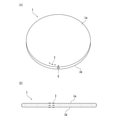
添付図面を参照して、本発明の実施形態について説明する。まず、本実施形態に係るウェーハについて説明する。図1(A)は、本実施形態に係るウェーハ1を模式的に示す斜視図であり、図1(B)は、本実施形態に係るウェーハ1を模式的に示す断面図である。
An embodiment of the present invention will be described with reference to the accompanying drawings. First, the wafer according to this embodiment will be described. FIG. 1A is a perspective view schematically showing the
ウェーハ1は、例えば、シリコン(Si)、シリコンカーバイド(SiC)、ガリウムナイトライド(GaN)、または、その他の半導体材料で形成された円板状の基板である。または、ウェーハ1は、タンタル酸リチウム(LT)及びニオブ酸リチウム(LN)等の複酸化物やサファイア(Al2O3)等の材料で形成される。
The
ウェーハ1の表面1aには、互いに交差する複数の分割予定ラインが設定され、該分割予定ラインによって区画された各領域にIC、LSI、LED等のデバイスが形成される。そして、該ウェーハを分割予定ラインに沿って分割すると個々のデバイスチップを形成できる。例えば、ウェーハ1がSiCインゴットである場合、ウェーハ1は、インバータやコンバータに代表されるパワーデバイス等の製造に用いられる。
A plurality of scheduled division lines intersecting each other are set on the surface 1a of the
本実施形態に係るウェーハ1には、抵抗率に関する情報を示す文字、数字、又はマーク3が表面1a、裏面1b、又は内部に形成される。抵抗率に関する情報を示す文字、数字、又はマーク3は、例えば、ウェーハ1にレーザビームを照射して該ウェーハ1を分割する際の該レーザビームの照射条件等の加工条件を決定する際に参照される。
On the
該文字、数字、又はマーク3がウェーハ1の内部に形成されている場合においても、ウェーハ1が透明であれば該文字、数字、又はマーク3を読み取ることができる。また、ウェーハ1が不透明である場合においても、ウェーハ1を透過する波長の光を使用することで該文字、数字、又はマーク3を読み取ることができる。該文字、数字、又はマーク3がウェーハ1の内部に形成されていると、ウェーハ1を加工しても該文字、数字、又はマーク3が失われにくい。
Even when the letters, numbers, or marks 3 are formed inside the
以下、抵抗率に関する情報を示す文字、数字、又はマーク3が形成されたウェーハ1を製造する過程と、該ウェーハ1を使用してデバイスチップを製造する過程と、を説明することで該ウェーハ1についてさらに説明する。
Hereinafter, the process of manufacturing a
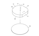
図2は、ウェーハ1の原料となるインゴット7を模式的に示す斜視図である。インゴット7は、例えば、溶融した部材に種結晶を接触させ該種結晶を引き上げるチョクラルスキー法により形成される。例えば、シリコン等の半導体材料でなる単結晶インゴットを製造する場合、溶融した部材にドーパントとしてホウ素またはリンを混入させてもよい。ただし、インゴット7の製造方法はこれに限定されない。
FIG. 2 is a perspective view schematically showing an
インゴット7が単結晶インゴットである場合、インゴット7の結晶方位を測定し、該結晶方位を示すノッチ5やオリエンテーションフラットと呼ばれる切り欠き部をインゴット7に形成する。この場合、インゴット7から切り出されたウェーハ1にもノッチ5等が残るため、該ノッチ5等を参照して該ウェーハ1の結晶方位を確認できる。
When the
次に、インゴット7からウェーハ1を製造する本実施形態に係るウェーハ1の製造方法について説明する。図12(A)は、本実施形態に係るウェーハ1の製造方法の各ステップのフローを説明するフローチャートである。
Next, a method for manufacturing the
本実施形態に係るウェーハ1の製造方法では、まず、インゴット7をスライスして複数のウェーハ1を生成するスライスステップS10を実施する。スライスステップS10では、例えば、ワイヤー状の鋸刃を有するワイヤーソー(不図示)を用いてインゴット7を切断する。円柱状のインゴット7を、所定の間隔でその伸長方向に垂直な面に沿ってワイヤーソーで切断すると、ウェーハ1が切り出される。
In the method for manufacturing a
ここで、ワイヤーソーで切り出された直後のウェーハ1の表面1a及び裏面1bには、ワイヤーソーに起因する加工歪層が形成されている。そこで、ウェーハ1の表面1a及び裏面1bを研削して所定の厚さに薄化し、その後にウェーハ1の表面1a及び裏面1bを研磨して鏡面といえる程度の平坦面に仕上げる。すると、デバイスを形成するのに適した状態の所定の厚さのウェーハ1が得られる。
Here, a processing strain layer due to the wire saw is formed on the front surface 1a and the
すなわち、スライスステップS10を実施した後、該スライスステップS10で生成されたウェーハ1を所定の厚みに研削加工する研削ステップS20と、研削されたウェーハ1を研磨する研磨ステップS30と、を実施する。図3は、研削ステップS20を模式的に示す斜視図である。
That is, after performing the slice step S10, a grinding step S20 for grinding the
研削ステップS20では、研削装置2が使用される。研削装置2は、被加工物となるウェーハ1を吸引保持するチャックテーブル4と、該チャックテーブル4に保持された被加工物を研削する研削ユニット6と、を備える。チャックテーブル4は、ウェーハ1と同等の径の多孔質部材(不図示)を上面に備え、該上面はウェーハ1が載せられる保持面4aとなる。該多孔質部材は図示しない吸引源に接続されており、チャックテーブル4は保持面4aに載せられたウェーハ1を吸引保持できる。
In the grinding step S20, the grinding
研削ユニット6は、保持面4aに略垂直な方向に沿ったスピンドル8と、スピンドル8の上端に接続されたモータ等の回転駆動源(不図示)と、を備える。スピンドル8の下端にはウェーハ1と同程度の径の円板状のホイールマウント10が設けられており、ホイールマウント10の下面には円環状の研削ホイール14がボルト等の固定具12により固定される。研削ホイール14の下面には、円環状に並ぶ研削砥石16が装着されている。研削砥石16は、ダイヤモンド等の砥粒と、該砥粒を分散固定する結合材と、を有する。
The grinding unit 6 includes a
研削ステップS20では、まず、チャックテーブル4の保持面4a上にウェーハ1を載せる。そして、吸引源を作動させ、チャックテーブル4でウェーハ1を吸引保持する。このとき、ウェーハ1の被研削面を上方に露出させ、反対側の面を保持面4aに対面させる。また、このとき、研削されるウェーハ1の研削されない面を保護するために、予め該面に保護部材9が貼着されてもよい。
In the grinding step S20, first, the
そして、チャックテーブル4を保持面4aに略垂直な軸の周りに回転させるとともに、スピンドル8を回転させる。その後、チャックテーブル4と、研削ユニット6と、を互いに近づくように相対的に移動させ、円環軌道上を移動する研削砥石16をウェーハ1の被研削面に接触させる。すると、ウェーハ1が研削されて薄化される。
Then, the chuck table 4 is rotated around an axis substantially perpendicular to the holding
ウェーハ1の一方の面の研削が完了した後、同様にウェーハ1の他方の面を研削し、該ウェーハ1の両面の研削を完了させる。すると、ワイヤーソーによるインゴット11の切断に起因してウェーハ1の表面1a及び裏面1bに形成されていた加工歪層が薄くなるとともに、ウェーハ1が所定の厚さに薄化される。
After the grinding of one surface of the
研削ステップS20を実施した後、該研削ステップS20で研削されたウェーハ1の表面1aまたは裏面1bの一方または両方を研磨する研磨ステップS30を実施する。図4は、研磨ステップS30を模式的に示す斜視図である。研磨ステップS30では、研磨装置18が使用される。研磨装置18は、研削装置2と同様に構成されており、ウェーハ1を吸引保持するチャックテーブル20と、ウェーハ1を研磨する研磨ユニット22と、を備える。
After performing the grinding step S20, a polishing step S30 for polishing one or both of the front surface 1a and the
チャックテーブル4の上面は、保持面20aとなる。研磨ユニット22は、スピンドル24と、スピンドル24の上端に接続されたモータ等の回転駆動源(不図示)と、を備える。スピンドル24の下端にはホイールマウント26が設けられており、ホイールマウント26の下面には研磨ホイール30が固定具28により固定される。研磨ホイール30の下面には、研磨パッド32が固定されている。
The upper surface of the chuck table 4 is a holding
研磨ステップS30では、研削ステップS20と同様に、チャックテーブル20及びスピンドル24を回転させながら、研磨パッド32をウェーハ1の被研磨面に接触させる。なお、研磨ステップS30では、ウェーハ1の被研磨面とは反対側の面に予め保護部材9aが貼着されてもよい。
In the polishing step S30, similarly to the grinding step S20, the
研磨ステップS30では、ウェーハ1の表面1a及び裏面1bのうち少なくともデバイスが形成される一方の面が研磨されることが好ましく、両面が研磨されることがさらに好ましい。研磨ステップS30を実施すると、被研磨面に形成されていた加工歪層が除去され、ウェーハ1が鏡面に加工される。
In the polishing step S30, it is preferable that at least one of the front surface 1a and the
本実施形態に係るウェーハの製造方法では、さらに、ウェーハ1の抵抗率を測定する抵抗率測定ステップS40と、測定された抵抗率に関する情報を示す文字、数字、又はマーク3を形成する情報印字ステップS50と、を実施する。抵抗率測定ステップS40及び情報印字ステップS50は、スライスステップS10が実施された後に実施される。例えば、研削ステップS20の前、又は研磨ステップS30の次に実施されるとよい。
In the method for manufacturing a wafer according to the present embodiment, a resistivity measurement step S40 for measuring the resistivity of the
抵抗率測定ステップS40では、既知の方法でウェーハ1の抵抗率が測定される。例えば、渦電流法でウェーハ1の抵抗率を測定するナプソン株式会社製の抵抗測定器“EC-80C”を使用してウェーハ1の抵抗率を測定できる。または、4端子法等の接触式の抵抗測定器でウェーハ1の抵抗率を測定してもよい。ウェーハ1の抵抗率の測定方法に特に限定はないが、非接触式の抵抗測定器を使用するとウェーハ1に損傷等が生じにくいため、非接触式の抵抗測定器の使用が好ましい。
In the resistivity measurement step S40, the resistivity of the
情報印字ステップS50では、抵抗率測定ステップS40で測定され得られたウェーハ1の抵抗率に関する情報を示す文字、数字、又はマーク3をウェーハ1に形成する。図5は、情報印字ステップS50の一例を模式的に示す斜視図である。情報印字ステップS50は、例えば、レーザ加工装置34で実施される。
In the information printing step S50, characters, numbers, or marks 3 indicating information regarding the resistivity of the
レーザ加工装置34は、上面がウェーハ1を吸引保持する保持面36aとなるチャックテーブル36と、チャックテーブル36で保持されたウェーハ1にレーザビームを照射してウェーハ1をレーザ加工するレーザ加工ユニット38と、を備える。チャックテーブル36は、研削装置2のチャックテーブル4と同様に構成される。レーザ加工ユニット38は、レーザビームを発するレーザ発振器(不図示)と、レーザ発振器で発せられたレーザビームを集光する集光レンズ(不図示)と、を備える。
The
レーザ加工ユニット38は、例えば、ウェーハ1を透過する波長のレーザビーム38aをウェーハ1の内部の所定の高さ位置に集光し、集光点の近傍に改質層を形成できる。例えば、ウェーハ1がSiCウェーハである場合、表面1aから100μm程度下方の高さ位置に集光させるように下記の条件でレーザビーム38aを照射する。
波長 :1064nm
繰り返し周波数:140kHz
平均出力 :1.0W
The
Wavelength: 1064 nm
Repeat frequency: 140kHz
Average output: 1.0W
チャックテーブル36と、レーザ加工ユニット38と、は保持面36aに平行な方向に相対的に移動できる。ウェーハ1にレーザビーム38aを照射しながらチャックテーブル36と、レーザ加工ユニット38と、を相対的に移動させると集光点の位置を制御でき、改質層を所望の位置に形成できる。そして、情報印字ステップS50では、例えば、所定の平面形状の改質層をウェーハ1の内部に形成することで、ウェーハ1の抵抗率に関する情報を示す文字、数字、又は記号3を形成する。
The chuck table 36 and the
なお、ウェーハ1の抵抗率に関する情報を示す文字、数字、又は記号3は、ウェーハ1の内部ではなく、表面1a、又は裏面1bに形成されてもよい。この場合、例えば、レーザ加工装置34でウェーハ1が吸収する波長のレーザビーム38aをウェーハ1の表面1a、又は裏面1bに集光させ、アブレーションによりウェーハ1の表面1aに加工痕を形成する。すなわち、所定の形状の加工痕を形成することで表面1a、又は裏面1bに文字、数字、又は記号3を刻印する。
The characters, numbers, or
ここで、抵抗率に関する情報を示す文字、数字、又は記号3は、例えば、抵抗率測定ステップS40で得られたウェーハ1の抵抗率の測定値そのものを示す数字と、該測定値の単位を示す文字と、の組み合わせである。または、抵抗率を複数の所定の階級で分級したときの該抵抗率が所属する階級を示す文字等である。または、該抵抗率の測定値、又は該抵抗率が所属する階級の情報が格納されたバーコードや2次元コード等の記号でもよい。
Here, the characters, numbers, or
以上に説明する通り、本実施形態に係るウェーハの製造方法によると、抵抗率に関する情報を示す文字、数字、又は記号3が表面1a、裏面1b、又は内部のうち少なくとも一つに形成されたウェーハ1を製造できる。
As described above, according to the wafer manufacturing method according to the present embodiment, a wafer in which characters, numbers, or
製造されたウェーハ1の表面1aにはその後に複数のデバイスが形成され、その後に該ウェーハ1をデバイス毎に分割すると、個々のデバイスチップが得られる。ウェーハ1に形成された抵抗率に関する情報を示す文字、数字、又は記号3は、ウェーハ1を分割する際に読み出されてウェーハ1を分割する際のレーザビームの照射条件等の加工条件を決定する際に参照される。
A plurality of devices are subsequently formed on the surface 1a of the manufactured
なお、ウェーハ1は他の方法によりインゴットから切り出されて製造されてもよい。次に、他の実施形態に係るウェーハの製造方法について説明する。該他の実施形態に係るウェーハの製造方法では、円柱状のインゴット11の内部の所定の深さに分離面を設定し、該分離面に沿って剥離層となる改質層を形成し、該インゴット11を該剥離層で分断してウェーハ1を製造する。
The
図6には、インゴット11を模式的に示す斜視図が含まれている。図8(B)は、剥離層23を構成する改質層25及びクラック27が形成されたインゴット11を拡大して模式的に示す断面図である。インゴット11は、表面11aと、該表面11aの反対側の裏面11bと、を有する。表面11a及び裏面11bは、互いに平行である。
FIG. 6 includes a perspective view schematically showing the
例えば、インゴット11が単結晶SiCインゴットである場合、図6に示す通り、第1のオリエンテーションフラット13と、第1のオリエンテーションフラット13に直交する第2のオリエンテーションフラット15と、が形成される。第1のオリエンテーションフラット13の長さは、第2のオリエンテーションフラット15の長さより長く形成される。
For example, when the
単結晶SiCインゴットであるインゴット11は、端面(表面11a)の法線17に対して第2のオリエンテーションフラット15方向にオフ角α傾斜したc軸19と、c軸19に直交するc面21と、を有している。該c軸19は、例えば、端面(表面11a)から該端面と反対側の対向端面(裏面11b)に至る。c面21は、インゴット11の表面11aに対してオフ角αで傾いている。一般的に、SiCインゴットでは、短い第2のオリエンテーションフラット15の伸長方向に直交する方向がc軸19の傾斜方向となる。
The
c面21は、SiCインゴット中に分子レベルで無数に設定される。オフ角αは、例えば、4°に設定される。しかし、オフ角αは4°に限定されるものではなく、例えば、1°~6°の範囲で自由に設定してSiCインゴットを製造することができる。ただし、インゴット11はSiCインゴットに限定されない。
The c-
該他の実施形態に係るウェーハの製造方法の各ステップについて説明する。図12(B)は、該他の実施形態に係るウェーハの製造方法の各ステップの流れを説明するフローチャートである。該ウェーハの製造方法では、まず、インゴット11の端面(表面11aまたは裏面11b)を平坦化する平坦化ステップS60を実施する。なお、図6に示す通り、平坦化ステップS60を実施する前に、インゴット11の研磨される該端面とは反対側の面に保護部材9bを貼着してもよい。
Each step of the wafer manufacturing method according to the other embodiment will be described. FIG. 12B is a flowchart illustrating the flow of each step of the wafer manufacturing method according to the other embodiment. In the method for manufacturing the wafer, first, a flattening step S60 for flattening the end face (
平坦化ステップS60では、後述の通りレーザビームの被照射面となるインゴット11の該端面を研磨して平坦化する。該端面を平坦化すると、レーザビームが該端面からインゴット11の内部に整然と入射し、該レーザビームを所定の位置に適切に集光できる。平坦化ステップS60では、例えば、図4で説明した研磨装置18を使用してインゴット11の該端面を研磨する。
In the flattening step S60, the end surface of the
そして、平坦化ステップS60を実施した後、平坦化された該端面でインゴット11の抵抗率を測定する抵抗率測定ステップS70を実施する。なお、抵抗率測定ステップS70は、上述の抵抗率測定ステップS40と同様に実施される。
Then, after carrying out the flattening step S60, the resistivity measuring step S70 for measuring the resistivity of the
次に、剥離層形成ステップS80が実施される。図7(A)は、剥離層形成ステップS80を模式的に示す斜視図であり、図7(B)は、剥離層形成ステップS80において剥離層23を構成する改質層25の形成途上にあるインゴット11を模式的に示す断面図である。そして、図8(A)は、改質層25が形成されたインゴット11を模式的に平面図であり、図8(B)は、剥離層23を構成する改質層25及びクラック27が形成されたインゴット11を拡大して模式的に示す断面図である。なお、図8(B)に示す断面図では、付されるべきハッチングが省略されている。
Next, the release layer forming step S80 is carried out. FIG. 7A is a perspective view schematically showing the release layer forming step S80, and FIG. 7B is in the process of forming the modified
剥離層形成ステップS80は、図5で説明したレーザ加工装置34と同様に構成されるレーザ加工装置40で実施される。レーザ加工装置40は、上面が保持面42aとなるチャックテーブル42と、チャックテーブル42で保持されたウェーハ1をレーザ加工できるレーザ加工ユニット44と、を備える。
The release layer forming step S80 is carried out by the
剥離層形成ステップS80では、まず、インゴット11をレーザ加工装置40のチャックテーブル42の上に載せ、チャックテーブル42の吸引保持機構を作動させ、チャックテーブル42にインゴット11を吸引保持させる。次に、レーザ加工ユニット44をインゴット11の上方に移動させ、レーザ加工ユニット44の光学系を調整し、または、レーザ加工ユニット44の高さを調整し、レーザ加工ユニット44から発せられる第1のレーザビーム44aの集光点44bを所定の高さ位置に位置付ける。
In the release layer forming step S80, first, the
ここで、第1のレーザビーム44aの集光点44bが位置付けられる所定の高さとは、予めインゴット11の表面11aから所定の深さに設定される分離面の高さ位置である。分離面は、インゴット11の内部に表面11aに平行に設定される面であり、インゴット11の分断が予定された面である。分離面は、インゴット11から製造されるウェーハ1の厚さに相当する深さでインゴット11の表面11aから離間した面とされる。
Here, the predetermined height at which the
剥離層形成ステップS80では、インゴット11に対して透過性を有する波長の第1のレーザビーム44aの集光点44bを該分離面に位置付ける。そして、集光点44b及びチャックテーブル42を該分離面に沿って相対的に移動させながら第1のレーザビーム44aを表面11a側からインゴット11に照射する。
In the release layer forming step S80, the focusing
より詳細には、剥離層形成ステップS80では、インゴット11と、集光点44bと、を第1の方向に相対的に移動させ直線状の改質層25を形成する加工送りステップS81と、第2の方向に相対的に移動させる割り出し送りステップS82と、を繰り返す。
More specifically, in the peeling layer forming step S80, the processing feed step S81 for forming the linear modified
ここで、該第1の方向とは、オフ角αが形成される方向と直交する方向かつ該端面(表面11a)に平行な方向であり、オリエンテーションフラット15に平行な方向である。また、該第2の方向とは、オフ角αが形成される方向かつ該端面(表面11a)に平行な方向であり、オリエンテーションフラット13に平行な方向である。
Here, the first direction is a direction orthogonal to the direction in which the off-angle α is formed, a direction parallel to the end surface (
インゴット11の内部にレーザビーム44aを集光させると、集光点44bの近傍に改質層25が形成される。さらに、形成された改質層25からはクラック27が伸長する。例えば、インゴット11がSiCインゴットである場合、第2のオリエンテーションフラット15に沿って改質層25を形成すると、インゴット11のc面21(図8(B)等参照)に沿ってクラック27が伸長しやすい傾向にある。
When the
そして、分離面に沿って複数の直線状の改質層25を形成し、それぞれの改質層25からクラック27を伸長させると、分離面の全域に改質層25またはクラック27が形成された状態となる。なお、図7(A)、図7(B)、及び図8(A)では、説明の便宜のために、インゴット11の内部に形成される改質層25を破線で示しており、クラック27を省略している。
Then, when a plurality of linear modified
分離面に沿って改質層25及びクラック27が形成されると、インゴット11は改質層25及びクラック27を起点に分離しやすくなる。すなわち、改質層25及びクラック27は、剥離層23として機能する。剥離層形成ステップS80では、改質層25と、該改質層25から伸長するクラック27と、を含む剥離層23が該分離面に沿ってインゴット11の内部に形成される。
When the modified
ここで、第1のレーザビーム44aの照射条件について説明する。インゴット11を透過する波長の第1のレーザビーム44aを該インゴット11に照射するとき、集光点44bに適切な条件で第1のレーザビーム44aを到達させるために、インゴット11の該波長の光の透過率により該照射条件を調整する必要がある。
Here, the irradiation conditions of the
そして、インゴット11の光の透過率は、インゴット11に含まれる不純物の濃度に依存する。また、インゴット11に含まれる不純物の濃度により該インゴット11の抵抗率も変化する。そのため、インゴット11の抵抗率を測定し、該抵抗率に基づいて第1のレーザビーム44aの照射条件を決定できる。そこで、剥離層形成ステップS80では、抵抗率測定ステップS70で測定されたインゴット11の抵抗率に基づいて第1のレーザビーム44aの照射条件を決定するとよい。
The light transmittance of the
例えば、インゴット11がSiCインゴットである場合、抵抗率測定ステップS70で測定されたインゴット11の抵抗率が100mΩ・cm以下であると、該インゴット11は低抵抗品であるといえる。特に、インゴット11が抵抗率16mΩ・cm以上22mΩ・cm以下の低抵抗品である場合、以下の照射条件で第1のレーザビーム44aをインゴット11に照射するとよい。
波長 :1064nm
繰り返し周波数:30kHz
平均出力 :5.4W
集光深さ :300μm
For example, when the
Wavelength: 1064 nm
Repeat frequency: 30kHz
Average output: 5.4W
Optical depth: 300 μm
また、例えば、抵抗率測定ステップS70で測定された結果、SiCインゴットであるインゴット11が低抵抗品とはいえない場合、以下の照射条件で第1のレーザビーム44aをインゴット11に照射するとよい。
波長 :1064nm
繰り返し周波数:80kHz
平均出力 :3.2W
集光深さ :300μm
Further, for example, when the
Wavelength: 1064 nm
Repeat frequency: 80kHz
Average output: 3.2W
Optical depth: 300 μm
このように、剥離層形成ステップS80では、インゴット11の抵抗率に応じて第1のレーザビーム44aの照射条件を調整することで、インゴット11の内部に剥離層23を適切に形成できる。なお、インゴット11の抵抗率に基づいて調整される条件は上記に限定されず、他の条件が調整されてもよい。
As described above, in the release layer forming step S80, the
次に、情報印字ステップS90について説明する。情報印字ステップS90は、上述の情報印字ステップS50と同様に実施できるため、情報印字ステップS50の説明を適宜参照できる。図9は、情報印字ステップS90を模式的に示す斜視図である。情報印字ステップS50は、例えば、剥離層形成ステップS80が実施されたレーザ加工装置40で該剥離層形成ステップS80に引き続き実施されてもよい。
Next, the information printing step S90 will be described. Since the information printing step S90 can be performed in the same manner as the information printing step S50 described above, the description of the information printing step S50 can be appropriately referred to. FIG. 9 is a perspective view schematically showing the information printing step S90. The information printing step S50 may be continuously carried out, for example, in the
情報印字ステップS90では、剥離層23でインゴット11から剥離されて生成されるウェーハ1にその後にデバイスが形成されない領域に抵抗率測定ステップS70で測定されたインゴット11の抵抗率に関する情報を示す文字、数字、又はマーク3を形成する。該文字、数字、又はマーク3は、例えば、インゴット11の端部に形成される。
In the information printing step S90, characters indicating information regarding the resistivity of the
ここで、情報印字ステップS90では、該文字、数字、又はマーク3は、レーザ加工ユニット44から発せられる第2のレーザビーム44cによりインゴット11の平坦化された端面(表面11a)、又は内部の一方、又は両方に形成される。
Here, in the information printing step S90, the characters, numbers, or marks 3 are flattened end faces (
例えば、インゴット11の内部の剥離層23よりも浅い高さ位置に該インゴット11を透過する波長の第2のレーザビーム44cを集光して改質層を形成し、該改質層で構成される文字、数字、又はマーク3を形成するとよい。この場合、第2のレーザビーム44cの波長はインゴット11を透過する波長とするとよく、下記の照射条件でインゴット11に照射するとよい。
波長 :1064nm
繰り返し周波数:140kHz
平均出力 :1.0W
集光深さ :100μm
For example, a
Wavelength: 1064 nm
Repeat frequency: 140kHz
Average output: 1.0W
Optical depth: 100 μm
また、インゴット11の表面11aに該文字、数字、又はマーク3を形成する場合、インゴット11に吸収される波長の第2のレーザビーム44cを該インゴット11の表面11aに集光し、アブレーション加工により該文字、数字、又はマーク3を形成するとよい。
When the letters, numbers, or marks 3 are formed on the
なお、情報印字ステップS90は、剥離層形成ステップS80の前に実施しても、剥離層形成ステップS80の後に実施してもよい。ただし、剥離層形成ステップS80の後に情報印字ステップS90を実施すると、インゴット11に形成された該文字、数字、又はマーク3が剥離層23の形成を妨げることがない。
The information printing step S90 may be performed before the release layer forming step S80 or after the release layer forming step S80. However, when the information printing step S90 is performed after the peeling layer forming step S80, the characters, numbers, or marks 3 formed on the
情報印字ステップS90を実施した後、インゴット11を剥離層23を起点として分割し、生成されたウェーハ1を剥離して該ウェーハ1を生成するウェーハ生成ステップS100を実施する。ウェーハ生成ステップS100では、例えば、内部に剥離層23が形成されたインゴット11に超音波振動を付与することでインゴット11を分割する。ただし、ウェーハ1の剥離方法はこれに限定されない。
After performing the information printing step S90, the
インゴット11を分割すると、内部、又は表面に抵抗率に関する情報を示す文字、数字、又はマーク3が形成されたウェーハ1が得られる。以上に説明する通り、図12(B)のフローチャートで説明されるウェーハ1の製造方法によると、内部、又は表面に抵抗率に関する情報を示す文字、数字、又はマーク3が形成されたウェーハ1が製造される。
When the
次に、抵抗率に関する情報を示す文字、数字、又はマーク3が形成され、さらに、表面1aに複数のデバイスが形成されたウェーハ1をレーザ加工して分割し、複数のデバイスチップを製造するデバイスチップの製造方法について説明する。図12(C)は、該デバイスチップの製造方法の各ステップの流れを説明するフローチャートである。
Next, a device for manufacturing a plurality of device chips by laser-machining and dividing a
図10(A)には、レーザ加工されるウェーハ1を模式的に示す斜視図が含まれている。まず、ウェーハ1について説明する。該デバイスチップの製造方法では、例えば、上述のウェーハの製造方法により製造されたウェーハ1が使用される。
FIG. 10A includes a perspective view schematically showing the
ウェーハ1には、表面1aに互いに交差する複数の分割予定ライン29が設定される。ウェーハ1の表面1aの分割予定ライン29で区画された各領域には、予めフォトリソグラフィ等のプロセスが実施されIC、LSI、又はLED等のデバイス31が形成される。
A plurality of scheduled division lines 29 intersecting each other on the surface 1a are set on the
また、レーザ加工されるウェーハ1は、ダイシングテープと呼ばれるテープ33を介して金属等の材料で形成されたリングフレーム35と予め一体化され、フレームユニット37の一部として取り扱われる。ウェーハ1を含むフレームユニット37を形成すると、ウェーハ1及び製造されるデバイスチップの取り扱いが容易となり、ウェーハ1等の損傷を防止できる。
Further, the laser-processed
ウェーハ1のレーザ加工は、図10(A)に示すレーザ加工装置46が使用される。レーザ加工装置46は、上述のレーザ加工装置34,40と同様に構成される。図10(A)では、フレームユニット37を保持するチャックテーブルが省略されている。
The
該デバイスチップの製造方法では、まず、フレームユニット37の状態のウェーハ1をレーザ加工装置46に搬入する搬入ステップS110を実施する。搬入ステップS110では、チャックテーブル(不図示)にフレームユニット37の状態のウェーハ1を載せ、テープ33を介して該チャックテーブルでウェーハ1を吸引保持する。そして、レーザ加工ユニット48の下方にウェーハ1を位置付ける。
In the method for manufacturing the device chip, first, a carry-in step S110 is carried out in which the
次に、ウェーハ1をレーザ加工ユニット48でレーザ加工するレーザ加工ステップS120を実施する。図10(A)は、レーザ加工ステップS120を模式的に示す斜視図であり、図10(B)は、レーザ加工されているウェーハ1を模式的に示す断面図である。
Next, a laser machining step S120 for laser machining the
レーザ加工ステップS120では、ウェーハ1を透過する波長のレーザビーム48aの集光点48bをウェーハ1の内部に位置付け、表面1aに平行な方向に集光点48b及びウェーハ1を相対的に移動させながらレーザビーム48aを集光点48bに照射する。これにより、ウェーハ1の内部に分割予定ライン29に沿った改質層39を形成する。
In the laser processing step S120, the
より詳細に説明する。まず、チャックテーブルを回転させウェーハ1の分割予定ライン29をレーザ加工装置46の加工送り方向に合わせる。また、分割予定ライン29の延長線の上方にレーザ加工ユニット48が配設されるように、チャックテーブル及びレーザ加工ユニット48の相対位置を調整する。そして、レーザビーム48aの集光点48bを所定の高さ位置に位置付ける。
It will be explained in more detail. First, the chuck table is rotated to align the planned
次に、レーザ加工ユニット48からウェーハ1の内部にレーザビーム48aを照射しながらチャックテーブルと、レーザ加工ユニット48と、を該チャックテーブルの上面に平行な加工送り方向に沿って相対移動させる。すなわち、レーザビーム48aの集光点48bをウェーハ1の内部に位置付け、レーザビーム48aを分割予定ライン29に沿ってウェーハ1に照射する。すると、改質層39がウェーハ1の内部に形成される。なお、図10(A)においては、ウェーハ1の内部に形成された改質層39を破線で示している。
Next, the chuck table and the
一つの分割予定ライン29に沿ってウェーハ1の内部に改質層39を形成した後、チャックテーブル及びレーザ加工ユニット48を加工送り方向とは垂直な割り出し送り方向に相対的に移動させ、他の分割予定ライン29に沿って同様にウェーハ1をレーザ加工する。一つの方向に沿った全ての分割予定ライン29に沿って改質層39を形成した後、チャックテーブルを保持面に垂直な軸の回りに回転させ、他の方向に沿った分割予定ライン29に沿って同様にウェーハ1をレーザ加工する。
After forming the reforming
ここで、レーザ加工ステップS120では、ウェーハ1の抵抗率に関する情報を示す文字、数字、又はマーク3を読み取り、ウェーハ1の抵抗率に基づいてレーザビーム48aの照射条件を決定する。例えば、ウェーハ1が低抵抗なSiCウェーハである場合、レーザ加工ステップS120におけるレーザビーム48aの照射条件は、例えば、以下のように設定される。
波長 :1342nm
繰り返し周波数:90kHz
平均出力 :2.2W
加工送り速度 :700mm/秒
Here, in the laser processing step S120, characters, numbers, or marks 3 indicating information regarding the resistivity of the
Wavelength: 1342nm
Repeat frequency: 90kHz
Average output: 2.2W
Machining feed rate: 700 mm / sec
また、ウェーハ1が高抵抗なSiCウェーハである場合、レーザ加工ステップS120におけるレーザビーム48aの照射条件は、例えば、以下のように設定される。
波長 :1342nm
繰り返し周波数:90kHz
平均出力 :1.7W
加工送り速度 :700mm/秒
When the
Wavelength: 1342nm
Repeat frequency: 90kHz
Average output: 1.7W
Machining feed rate: 700 mm / sec
なお、レーザ加工ステップS120では、ウェーハ1の抵抗率から想定されるウェーハ1の性質に基づいた照射条件でレーザビーム48aがウェーハ1に照射されればよい。例えば、同種の複数のウェーハ1を次々にレーザ加工して分割する場合において、すべてのウェーハ1について該文字、数字、又はマーク3が読み取られて該照射条件が都度変更される必要はない。
In the laser processing step S120, the
すなわち、ウェーハ1の抵抗率に関する情報を示す文字、数字、又はマーク3から取得できる該ウェーハ1の抵抗率に基づいて決定された照射条件でレーザビーム48aが該ウェーハに照射されればよい。複数の抵抗率が同じウェーハ1をレーザ加工する際、あるウェーハ1へレーザビーム48aを照射する際の照射条件は、他のウェーハ1に形成されていた該文字、数字、又はマーク3から取得できる抵抗率に基づいて決定されてもよい。
That is, the
また、該文字、数字、又はマーク3がウェーハ1の内部に形成されている場合、例えば、ウェーハ1を透過する波長の光を照射し、該光を検出できる受光素子で該文字、数字、又はマーク3を撮像するとよい。例えば、ウェーハ1が赤外線を透過する場合、該文字、数字、又はマーク3の撮像には赤外線を使用でき、赤外光源と、赤外線受光素子と、を備える撮像ユニットを使用して該文字、数字、又はマーク3を撮像するとよい。
When the letters, numbers, or marks 3 are formed inside the
レーザ加工ステップS120を実施した後、改質層39を起点にウェーハ1を分割することで複数のデバイスチップを製造する分割ステップS130を実施する。分割ステップS130では、ウェーハ1に貼着されたテープ33を径方向外側に拡張することでウェーハ1に力を加えてウェーハ1を分割する。分割ステップS130では、図11(A)及び図11(B)に示すエキスパンド装置50を使用するとよい。
After performing the laser processing step S120, the division step S130 for manufacturing a plurality of device chips by dividing the
エキスパンド装置50は、ウェーハ1の径よりも大きい径を有する円筒状のドラム52と、フレーム支持台58を含むフレーム保持ユニット54と、を備える。フレーム保持ユニット54のフレーム支持台58は、ドラム52の径よりも大きい径の開口を備え、該ドラム52の上端部と同様の高さに配設され、該ドラム52の上端部を外周側から囲む。
The expanding
フレーム支持台58の外周側には、クランプ56が配設される。フレーム支持台58の上にフレームユニット37を載せ、クランプ56によりフレームユニット37のフレーム35を把持させると、フレームユニット37がフレーム支持台58に固定される。
A
フレーム支持台58は、鉛直方向に沿って伸長する複数のロッド60により支持され、各ロッド60の下端部には、該ロッド60を昇降させるエアシリンダ62が配設される。各エアシリンダ62を作動させると、フレーム支持台58がドラム52に対して引き下げられる。
The
テープ33を拡張する際、まず、エキスパンド装置50のドラム52の上端の高さと、フレーム支持台58の上面の高さと、が一致するように、エアシリンダ62を作動させてフレーム支持台58の高さを調節する。次に、レーザ加工装置46から搬出されたフレームユニット37をエキスパンド装置50のドラム52及びフレーム支持台58の上に載せる。
When expanding the
その後、クランプ56によりフレーム支持台58の上にフレームユニット37のフレーム35を固定する。図11(A)は、フレーム支持台58の上に固定されたフレームユニット37を模式的に示す断面図である。ウェーハ1の内部には、分割予定ライン29に沿って改質層39が形成されている。
After that, the
次に、エアシリンダ62を作動させてフレーム保持ユニット54のフレーム支持台58をドラム52に対して引き下げる。すると、図11(B)に示す通り、テープ33が径方向外側に拡張される。図11(B)は、テープ33が拡張された状態のフレームユニット37を模式的に示す断面図である。
Next, the
テープ33が拡張されると、ウェーハ1に径方向外側に向いた力が働き、ウェーハ1が改質層39を起点として分割され、個々のデバイスチップ41が形成される。テープ33をさらに拡張すると、テープ33に支持された各デバイスチップ41の間隔が広げられ、個々のデバイスチップ41のピックアップが容易となる。
When the
以上に示す通り、本実施形態に係るウェーハ、ウェーハの製造方法、及びデバイスチップの製造方法では、ウェーハ1の抵抗率に関する情報を示す文字、数字、又はマーク3が該ウェーハ1に形成されている。そのため、ウェーハ1をレーザ加工して内部に改質層39を形成する際、該文字、数字、又はマーク3から取得できる該ウェーハ1の抵抗率に基づいてレーザビーム48aの照射条件を決定できる。
As described above, in the wafer, wafer manufacturing method, and device chip manufacturing method according to the present embodiment, characters, numbers, or marks 3 indicating information regarding the resistivity of the
ウェーハ1をレーザ加工してデバイスチップ41を製造する際、デバイス31が表面1aに形成された取り扱いに注意を要する該ウェーハ1の抵抗率を測定する必要がない。したがって、様々なウェーハ1に最適な照射条件でレーザビーム48aを照射して該ウェーハ1を容易かつ迅速にレーザ加工でき、ウェーハ1の加工効率を高めることができ、デバイスチップ41の製造効率も上がる。
When the
なお、本発明は上記実施形態の記載に限定されず、種々変更して実施可能である。例えば、上記実施形態では、ウェーハ1にレーザビーム48aを照射する照射条件を該ウェーハ1の抵抗率に基づいて調整し決定する場合について説明したが、本発明の一態様はこれに限定されない。すなわち、該照射条件は、ウェーハ1の抵抗率に加え、ウェーハ1の材質や形状、レーザビーム48aの集光深さ等の様々な要素が考慮されて決定されてもよい。
The present invention is not limited to the description of the above embodiment, and can be modified in various ways. For example, in the above embodiment, the case where the irradiation condition for irradiating the
上記実施形態に係る構造、方法等は、本発明の目的の範囲を逸脱しない限りにおいて適宜変更して実施できる。 The structure, method and the like according to the above embodiment can be appropriately modified and carried out as long as they do not deviate from the scope of the object of the present invention.
1 ウェーハ
1a 表面
1b 裏面
3 文字、数字、又はマーク
5 ノッチ
7 インゴット
9,9a,9b 保護部材
11 インゴット
13,15 オリエンテーションフラット
17 法線
19 c軸
21 c面
23 剥離層
25 改質層
27 クラック
29 分割予定ライン
31 デバイス
33 テープ
35 リングフレーム
37 フレームユニット
39 改質層
41 デバイスチップ
2 研削装置
4,20,36,42 チャックテーブル
4a,20a,36a,42a 保持面
6 研削ユニット
8,24 スピンドル
10,26 ホイールマウント
12,28 固定具
14 研削ホイール
16 研削砥石
18 研磨装置
22 研磨ユニット
30 研磨ホイール
32 研磨パッド
34,40,46 レーザ加工装置
38,44,48 レーザ加工ユニット
38a,44a,48a レーザビーム
44b 集光点
50 エキスパンド装置
52 ドラム
54 フレーム保持ユニット
56 クランプ
58 フレーム支持台
60 ロッド
62 エアシリンダ
1 Wafer
Claims (7)
該インゴットをスライスして複数の該ウェーハを生成するスライスステップと、
該スライスステップで生成された該ウェーハを所定の厚みに研削加工する研削ステップと、
該研削ステップで研削された該ウェーハの表面または裏面の一方または両方を研磨する研磨ステップと、
該ウェーハの抵抗率を測定する抵抗率測定ステップと、
該抵抗率測定ステップ後に、該ウェーハの該表面、該裏面、又は内部のいずれか一つ以上に該抵抗率に関する情報を示す文字、数字、又はマークを形成する情報印字ステップと、を備えることを特徴とするウェーハの製造方法。 A wafer manufacturing method that manufactures wafers from ingots.
A slicing step of slicing the ingot to produce multiple wafers.
A grinding step for grinding the wafer generated in the slice step to a predetermined thickness, and a grinding step.
A polishing step for polishing one or both of the front surface and the back surface of the wafer ground in the grinding step,
A resistivity measurement step for measuring the resistivity of the wafer, and
After the resistivity measurement step, any one or more of the front surface, the back surface, or the inside of the wafer is provided with an information printing step for forming characters, numbers, or marks indicating information on the resistivity. A characteristic wafer manufacturing method.
該インゴットの端面を平坦化する平坦化ステップと、
平坦化された該端面で該インゴットの抵抗率を測定する抵抗率測定ステップと、
該端面から該インゴットに対して透過性を有する波長の第1のレーザビームの集光点を生成すべき該ウェーハの厚みに相当する深さに位置づけて該第1のレーザビームを該インゴットに照射し、該インゴットの内部に剥離層を形成する剥離層形成ステップと、
生成すべき該ウェーハのデバイスが形成されない領域に第2のレーザビームの集光点を位置づけて該第2のレーザビームを該インゴットに照射し、該抵抗率測定ステップで測定された該抵抗率に関する情報を示す文字、数字、又はマークを該インゴットの平坦化された該端面、又は内部の一方、又は両方に形成する情報印字ステップと、
該インゴットを該剥離層を起点として分割し、生成された該ウェーハを剥離して該ウェーハを生成するウェーハ生成ステップを備えることを特徴とするウェーハの製造方法。 A wafer manufacturing method that manufactures wafers from ingots.
A flattening step for flattening the end face of the ingot,
A resistivity measurement step of measuring the resistivity of the ingot on the flattened end face,
The ingot is irradiated with the first laser beam at a depth corresponding to the thickness of the wafer to generate a focusing point of the first laser beam having a wavelength transparent to the ingot from the end face. Then, the release layer forming step of forming the release layer inside the ingot, and
With respect to the resistivity measured in the resistivity measurement step, the ingot is irradiated with the second laser beam by locating the condensing point of the second laser beam in the region where the device of the wafer to be generated is not formed. An information printing step that forms informational letters, numbers, or marks on the flattened end face of the ingot, or on one or both of the interiors.
A method for manufacturing a wafer, comprising a wafer generation step of dividing the ingot with the peeling layer as a starting point and peeling the generated wafer to generate the wafer.
該c軸は、該端面の法線に対して傾いており、
該c面は、該端面に対してオフ角で傾いており、
該剥離層形成ステップでは、該インゴットと、該第1のレーザビームの該集光点と、を該オフ角が形成される方向と直交する方向かつ該端面に平行な第1の方向に相対的に移動させ直線状の改質層を形成する加工送りステップと、該オフ角が形成される該方向かつ該端面に平行な第2の方向に該インゴットと、該集光点と、を相対的に移動させる割り出し送りステップと、を繰り返して該改質層を含む該剥離層を形成することを特徴とする請求項4記載のウェーハの製造方法。 The ingot is a single crystal SiC ingot having the end face, the facing end face opposite to the end face, the c-axis extending from the end face to the facing end face, and the c-plane orthogonal to the c-axis.
The c-axis is tilted with respect to the normal of the end face.
The c-plane is tilted at an off angle with respect to the end face.
In the exfoliation layer forming step, the ingot and the condensing point of the first laser beam are relative to each other in a direction orthogonal to the direction in which the off-angle is formed and in a first direction parallel to the end face. The ingot and the condensing point are relative to each other in the processing feed step of moving to to form a linear modified layer, and in the direction in which the off-angle is formed and in the second direction parallel to the end face. The method for manufacturing a wafer according to claim 4, wherein the peeling layer including the modified layer is formed by repeating the indexing feed step of moving to.
該ウェーハをレーザ加工装置に搬入する搬入ステップと、
該ウェーハを透過する波長のレーザビームの集光点を該ウェーハの内部に位置付け、該表面に平行な方向に該集光点及び該ウェーハを相対的に移動させながら該レーザビームを該集光点に照射し、該ウェーハの内部に該分割予定ラインに沿った改質層を形成するレーザ加工ステップと、
該改質層を起点に該ウェーハを分割することで複数の該デバイスチップを製造する分割ステップと、を有し、
該ウェーハには、該ウェーハの抵抗率に関する情報を示す文字、数字、又はマークが形成されており、
該レーザ加工ステップでは、該ウェーハの抵抗率に関する情報を示す文字、数字、又はマークから取得できる該ウェーハの抵抗率に基づいて決定された照射条件で該レーザビームが該ウェーハに照射されることを特徴とするデバイスチップの製造方法。 A device for manufacturing a plurality of device chips by laser-machining a wafer in which a plurality of planned division lines intersecting each other are set on the surface and a device is formed in each region of the planned division line on the surface. It ’s a chip manufacturing method.
The carry-in step of carrying the wafer into the laser processing device and
A focusing point of a laser beam having a wavelength transmitted through the wafer is positioned inside the wafer, and the laser beam is moved to the focusing point while relatively moving the focusing point and the wafer in a direction parallel to the surface. A laser processing step of irradiating the wafer to form a modified layer along the planned division line inside the wafer.
It has a division step of manufacturing a plurality of the device chips by dividing the wafer from the modified layer as a starting point.
The wafer is formed with letters, numbers, or marks indicating information about the resistivity of the wafer.
In the laser machining step, the laser beam is irradiated to the wafer under irradiation conditions determined based on the resistivity of the wafer that can be obtained from letters, numbers, or marks indicating information about the resistivity of the wafer. A characteristic device chip manufacturing method.
Priority Applications (4)
| Application Number | Priority Date | Filing Date | Title |
|---|---|---|---|
| JP2020131713A JP7479762B2 (en) | 2020-08-03 | 2020-08-03 | Manufacturing method for device chips |
| US17/382,921 US12011784B2 (en) | 2020-08-03 | 2021-07-22 | Wafer, wafer manufacturing method, device chip manufacturing method, and resistivity markings |
| DE102021207939.3A DE102021207939B4 (en) | 2020-08-03 | 2021-07-23 | WAFER MANUFACTURING METHODS AND COMPONENT CHIP MANUFACTURING METHODS |
| CN202110834950.4A CN114068301A (en) | 2020-08-03 | 2021-07-23 | Wafer, method for manufacturing wafer, and method for manufacturing device chip |
Applications Claiming Priority (1)
| Application Number | Priority Date | Filing Date | Title |
|---|---|---|---|
| JP2020131713A JP7479762B2 (en) | 2020-08-03 | 2020-08-03 | Manufacturing method for device chips |
Publications (2)
| Publication Number | Publication Date |
|---|---|
| JP2022028362A true JP2022028362A (en) | 2022-02-16 |
| JP7479762B2 JP7479762B2 (en) | 2024-05-09 |
Family
ID=79300745
Family Applications (1)
| Application Number | Title | Priority Date | Filing Date |
|---|---|---|---|
| JP2020131713A Active JP7479762B2 (en) | 2020-08-03 | 2020-08-03 | Manufacturing method for device chips |
Country Status (4)
| Country | Link |
|---|---|
| US (1) | US12011784B2 (en) |
| JP (1) | JP7479762B2 (en) |
| CN (1) | CN114068301A (en) |
| DE (1) | DE102021207939B4 (en) |
Cited By (1)
| Publication number | Priority date | Publication date | Assignee | Title |
|---|---|---|---|---|
| JP2023181853A (en) * | 2022-06-13 | 2023-12-25 | 株式会社ディスコ | Resistivity detection method and plate-shaped object processing method |
Families Citing this family (2)
| Publication number | Priority date | Publication date | Assignee | Title |
|---|---|---|---|---|
| JP7358107B2 (en) * | 2019-07-31 | 2023-10-10 | 株式会社ディスコ | laser processing equipment |
| CN116787002A (en) * | 2023-08-02 | 2023-09-22 | 迈为技术(珠海)有限公司 | Wafer laser cutting device and method based on liquid crystal spatial light modulator |
Citations (7)
| Publication number | Priority date | Publication date | Assignee | Title |
|---|---|---|---|---|
| JPS62193241A (en) * | 1986-02-20 | 1987-08-25 | Canon Inc | Crystal substrate for semiconductor device |
| JPH0750328A (en) * | 1993-08-04 | 1995-02-21 | Hitachi Cable Ltd | Semiconductor device manufacturing method, manufacturing apparatus thereof, and semiconductor device manufacturing wafer |
| JP2001076981A (en) * | 1999-09-03 | 2001-03-23 | Mitsubishi Materials Silicon Corp | Semiconductor wafer and method of manufacturing the same |
| JP2009081190A (en) * | 2007-09-25 | 2009-04-16 | Shin Etsu Handotai Co Ltd | Two-dimensional code printing wafer and its manufacturing method |
| JP2013055273A (en) * | 2011-09-06 | 2013-03-21 | Disco Abrasive Syst Ltd | Device chip and method of manufacturing device chip |
| JP2015154075A (en) * | 2014-02-11 | 2015-08-24 | サムスン エレクトロニクス カンパニー リミテッド | Wafer manufacturing method and wafer manufactured thereby |
| JP2020113664A (en) * | 2019-01-15 | 2020-07-27 | 株式会社ディスコ | Wafer and method for producing wafer |
Family Cites Families (8)
| Publication number | Priority date | Publication date | Assignee | Title |
|---|---|---|---|---|
| US5956596A (en) * | 1995-11-06 | 1999-09-21 | Samsung Electronics Co., Ltd. | Method of forming and cleaning a laser marking region at a round zone of a semiconductor wafer |
| US6303899B1 (en) * | 1998-12-11 | 2001-10-16 | Lsi Logic Corporation | Method and apparatus for scribing a code in an inactive outer clear out area of a semiconductor wafer |
| JP2004158768A (en) * | 2002-11-08 | 2004-06-03 | Disco Abrasive Syst Ltd | Semiconductor wafers and substrates |
| CN1938827B (en) | 2004-03-30 | 2010-05-26 | 浜松光子学株式会社 | Laser processing method and semiconductor chip |
| JP6395613B2 (en) | 2015-01-06 | 2018-09-26 | 株式会社ディスコ | Wafer generation method |
| JP2019033134A (en) * | 2017-08-04 | 2019-02-28 | 株式会社ディスコ | Wafer generation method |
| JP6998149B2 (en) | 2017-08-08 | 2022-01-18 | 株式会社ディスコ | Laser processing method |
| JP7443053B2 (en) * | 2019-12-26 | 2024-03-05 | 株式会社ディスコ | laser processing equipment |
-
2020
- 2020-08-03 JP JP2020131713A patent/JP7479762B2/en active Active
-
2021
- 2021-07-22 US US17/382,921 patent/US12011784B2/en active Active
- 2021-07-23 DE DE102021207939.3A patent/DE102021207939B4/en active Active
- 2021-07-23 CN CN202110834950.4A patent/CN114068301A/en active Pending
Patent Citations (7)
| Publication number | Priority date | Publication date | Assignee | Title |
|---|---|---|---|---|
| JPS62193241A (en) * | 1986-02-20 | 1987-08-25 | Canon Inc | Crystal substrate for semiconductor device |
| JPH0750328A (en) * | 1993-08-04 | 1995-02-21 | Hitachi Cable Ltd | Semiconductor device manufacturing method, manufacturing apparatus thereof, and semiconductor device manufacturing wafer |
| JP2001076981A (en) * | 1999-09-03 | 2001-03-23 | Mitsubishi Materials Silicon Corp | Semiconductor wafer and method of manufacturing the same |
| JP2009081190A (en) * | 2007-09-25 | 2009-04-16 | Shin Etsu Handotai Co Ltd | Two-dimensional code printing wafer and its manufacturing method |
| JP2013055273A (en) * | 2011-09-06 | 2013-03-21 | Disco Abrasive Syst Ltd | Device chip and method of manufacturing device chip |
| JP2015154075A (en) * | 2014-02-11 | 2015-08-24 | サムスン エレクトロニクス カンパニー リミテッド | Wafer manufacturing method and wafer manufactured thereby |
| JP2020113664A (en) * | 2019-01-15 | 2020-07-27 | 株式会社ディスコ | Wafer and method for producing wafer |
Cited By (1)
| Publication number | Priority date | Publication date | Assignee | Title |
|---|---|---|---|---|
| JP2023181853A (en) * | 2022-06-13 | 2023-12-25 | 株式会社ディスコ | Resistivity detection method and plate-shaped object processing method |
Also Published As
| Publication number | Publication date |
|---|---|
| CN114068301A (en) | 2022-02-18 |
| JP7479762B2 (en) | 2024-05-09 |
| US20220032404A1 (en) | 2022-02-03 |
| DE102021207939B4 (en) | 2025-07-31 |
| US12011784B2 (en) | 2024-06-18 |
| DE102021207939A1 (en) | 2022-02-03 |
Similar Documents
| Publication | Publication Date | Title |
|---|---|---|
| CN106057737B (en) | Separation method of thin plates | |
| CN107877011B (en) | Production method of SiC wafer | |
| KR102419485B1 (en) | Method of reducing wafer thickness | |
| CN110349837B (en) | Chip production method | |
| KR102384101B1 (en) | Method of reducing wafer thickness | |
| CN108372434B (en) | Production method of SiC wafer | |
| CN110911268B (en) | Wafer production method and laser processing device | |
| CN105414776B (en) | SiC ingot slicing method | |
| KR102178776B1 (en) | METHOD FOR PRODUCING SiC WAFER | |
| KR102845019B1 (en) | METHOD FOR MACHINING SiC INGOT AND LASER MACHINING APPARATUS | |
| KR20200053410A (en) | Method and apparatus for detecting facet region, method for producing wafer and apparatus for laser processing | |
| JP7210292B2 (en) | Wafer generation method | |
| JP6324796B2 (en) | Single crystal substrate processing method | |
| KR20210048981A (en) | Processing method of sic ingot and laser machining apparatus | |
| CN110571131B (en) | Chamfer processing method | |
| CN114055645A (en) | Method for manufacturing Si substrate | |
| JP7479762B2 (en) | Manufacturing method for device chips | |
| JP2015032771A (en) | Method of manufacturing wafer | |
| JP2023026921A (en) | Wafer processing method | |
| JP2022076543A (en) | Method for generating wafer | |
| KR102929217B1 (en) | Method for separating a wafer | |
| CN113001262B (en) | Grinding method of workpiece | |
| JP5846764B2 (en) | Wafer processing method | |
| CN114589421B (en) | Method for processing SiC ingot and laser processing device | |
| JP2006202933A (en) | Wafer division method |
Legal Events
| Date | Code | Title | Description |
|---|---|---|---|
| A621 | Written request for application examination |
Free format text: JAPANESE INTERMEDIATE CODE: A621 Effective date: 20230629 |
|
| A977 | Report on retrieval |
Free format text: JAPANESE INTERMEDIATE CODE: A971007 Effective date: 20240314 |
|
| A131 | Notification of reasons for refusal |
Free format text: JAPANESE INTERMEDIATE CODE: A131 Effective date: 20240319 |
|
| A521 | Request for written amendment filed |
Free format text: JAPANESE INTERMEDIATE CODE: A523 Effective date: 20240409 |
|
| TRDD | Decision of grant or rejection written | ||
| A01 | Written decision to grant a patent or to grant a registration (utility model) |
Free format text: JAPANESE INTERMEDIATE CODE: A01 Effective date: 20240423 |
|
| A61 | First payment of annual fees (during grant procedure) |
Free format text: JAPANESE INTERMEDIATE CODE: A61 Effective date: 20240423 |
|
| R150 | Certificate of patent or registration of utility model |
Ref document number: 7479762 Country of ref document: JP Free format text: JAPANESE INTERMEDIATE CODE: R150 |